WO2012008106A1 - ダイレクトサンプリング回路 - Google Patents
ダイレクトサンプリング回路 Download PDFInfo
- Publication number
- WO2012008106A1 WO2012008106A1 PCT/JP2011/003709 JP2011003709W WO2012008106A1 WO 2012008106 A1 WO2012008106 A1 WO 2012008106A1 JP 2011003709 W JP2011003709 W JP 2011003709W WO 2012008106 A1 WO2012008106 A1 WO 2012008106A1
- Authority
- WO
- WIPO (PCT)
- Prior art keywords
- capacitor
- signal
- filter
- buffer
- switch
- Prior art date
- Legal status (The legal status is an assumption and is not a legal conclusion. Google has not performed a legal analysis and makes no representation as to the accuracy of the status listed.)
- Ceased
Links
Images




Classifications
-
- H—ELECTRICITY
- H03—ELECTRONIC CIRCUITRY
- H03K—PULSE TECHNIQUE
- H03K17/00—Electronic switching or gating, i.e. not by contact-making and –breaking
- H03K17/002—Switching arrangements with several input- or output terminals
- H03K17/005—Switching arrangements with several input- or output terminals with several inputs only
-
- H—ELECTRICITY
- H03—ELECTRONIC CIRCUITRY
- H03H—IMPEDANCE NETWORKS, e.g. RESONANT CIRCUITS; RESONATORS
- H03H15/00—Transversal filters
-
- G—PHYSICS
- G11—INFORMATION STORAGE
- G11C—STATIC STORES
- G11C27/00—Electric analogue stores, e.g. for storing instantaneous values
- G11C27/02—Sample-and-hold arrangements
- G11C27/024—Sample-and-hold arrangements using a capacitive memory element
Definitions
- the present invention relates to a direct sampling circuit that performs direct sampling processing on an input signal integrated in a time division manner.
- FIG. 1 generally shows a discrete time direct sampling circuit.
- the discrete time direct sampling circuit includes a voltage-current converter (TA) 1, a sampling switch 2, a history capacitor (C H ) 3, a rotation capacitor group 4a to 4h, a buffer capacitor (C B ) 5, and a dump switch. 6, a reset switch 7, integration switch groups 8 a to 8 h, discharge switch groups 9 a to 9 h, and a digital control unit 10.
- TA voltage-current converter
- C H history capacitor
- C B buffer capacitor
- Voltage-current converter (TA) 1 converts the received radio frequency (RF) signal into a current and outputs it as an analog RF current signal.
- the sampling switch 2 is composed of, for example, an FET, and samples an input analog RF current signal according to a local frequency signal input (LO).
- the history capacitor (C H ) 3 charges the electric charge supplied by the current output from the sampling switch 2.
- the rotation capacitor groups 4a to 4h are connected in parallel with the history capacitor 3 and the buffer capacitor 5 through a plurality of types of switches.
- the rotation capacitor groups 4a to 4h are composed of a plurality of rotation capacitors (C R ) that charge or discharge electric charges according to on / off control of each switch.
- the buffer capacitor (C B ) 5 is shared with the charge charged in the plurality of rotation capacitors 4 and buffers the charge signal.
- the dump switch 6 turns on and off the connection between each of the rotation capacitor groups 4a to 4h and the buffer capacitor 5.
- the reset switch 7 grounds the charge stored in the rotation capacitor 4 after sharing the charge with the buffer capacitor 5.
- the integration switch groups 8a to 8h are composed of a plurality of integration switches.
- the integration switch groups 8a to 8h turn on / off the connection between the history capacitor 3 and each rotation capacitor in the rotation capacitor groups 4a to 4h.
- the discharge switch groups 9a to 9h are composed of a plurality of discharge switches.
- the release switch groups 9a to 9h turn on / off the connection between each rotation capacitor and the buffer capacitor 5 in the rotation capacitor groups 4a to 4h.
- the dump switch 6, the reset switch 7, the integration switch groups 8a to 8h, and the discharge switch groups 9a to 9h are composed of, for example, FET (n-type).
- the n-type FET is turned on (conductive) when the gate voltage is high (high) and turned off (cut off) when the gate voltage is low (low).
- the digital control unit 10 generates and supplies control signals to the integration switch groups 8a to 8h, the discharge switch groups 9a to 9h, the dump switch 6 and the reset switch 7.
- the rotation capacitor C R are provided eight discrete time direct sampling circuit. Accordingly, it is assumed that eight integration switches 8a to 8h and eight discharge switches 9a to 9h are provided. Then, at the end of the numbering of each component, a to h are added in alphabetical order.
- the discrete-time direct sampling circuit may be configured to perform a differential operation, and the configuration is disclosed in Patent Document 1. However, the explanation is omitted here for simplicity.
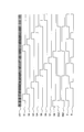
- FIG. 2 shows a timing chart of each control signal generated by the digital control unit 10.
- a local frequency signal (LO) is supplied to the gate of the sampling switch 2.
- the control signals S1 to S8 are supplied to the gates of the integration switches 8a to 8h, respectively.
- the control signal SAZ is supplied to the gates of the discharge switches 9a to 9d.
- the control signal SBZ is supplied to the gates of the discharge switches 9e to 9h.
- the control signal D is supplied to the gate of the dump switch 6, and the control signal R is supplied to the gate of the reset switch 7.
- the voltage-current converter 1 converts the input analog RF signal into an analog RF current signal and outputs the analog RF current signal to the sampling switch 2.
- the analog RF current signal is sampled by the sampling switch 2 with a local frequency signal LO having substantially the same frequency as the analog RF current signal.
- the signal sampled by the local frequency signal LO is converted into a discrete signal temporally discretized by integrating charges by the history capacitor 3 and the rotation capacitors 4a to 4h.
- a capacitor in parallel connection is configured by the history capacitor 3 and one of the rotation capacitor groups 4a to 4h.
- the discrete signal is integrated over a longer time than the clock length of the local frequency signal LO by the capacitor thus configured. Thereby, filter processing and decimation (decimation) are performed.
- the integration switch 8a is turned on by the control signal S1, and the rotation capacitor 4a is connected to the history capacitor 3. Then, the charges supplied to the two capacitors are integrated over a period during which the control signal S1 is high (for example, eight periods of the local frequency signal LO).
- the history capacitor 3 When the control signal S1 is low, the history capacitor 3 is turned off from the rotation capacitor 4a, and the control signal S2 is turned on from the rotation capacitor 4b.
- the rotation capacitor 4b integrates the charge supplied by the current of the discrete signal over the period when the control signal S2 is high, and then turns off the connection with the history capacitor 3.
- the rotation capacitors 4c to 4h are connected to the history capacitor 3 in turn every eight cycles of the local frequency signal LO by the control signals S3 to S8. Then, the charges supplied by the current of the discrete signal are integrated by the two capacitors.
- the discrete time direct sampling circuit integrates the electric charge supplied by the discrete signal current for eight cycles of the local frequency signal LO.
- the characteristics of an 8-tap FIR (Finite Impulse Response) filter are realized in the discrete-time direct sampling circuit.
- the sampling rate is decimated to 1/8.
- a functional unit that realizes this filter characteristic will be referred to as a first FIR filter.
- the rotation capacitor 4a to 4h is connected to the history capacitor 3 in order, thereby realizing the characteristics of an IIR (Infinite Impulse Response) filter.
- IIR Infinite Impulse Response
- a functional unit that realizes this filter characteristic will be referred to as a first IIR filter.
- the dump switch 6 is turned off by the control signal D, and the charge sharing state is canceled.
- the reset switch 7 is turned on by the control signal R, and the charges remaining in the rotation capacitors 4a to 4d are reset by grounding.
- the characteristics of the 4-tap FIR filter are realized by moving a part of the charges charged in each of the rotation capacitors 4a to 4d to the buffer capacitor 5 and synthesizing them.
- the In the discrete time direct sampling circuit discrete signals for 4 samples are synthesized and a discrete signal for 1 sample is output, so the sampling rate is decimated to 1 ⁇ 4.
- the IIR filter characteristics are realized by making each group of the rotation capacitors 4a to 4d and 4e to 4h alternately share a charge with the buffer capacitor 5. This filter characteristic will be referred to as a second IIR filter.
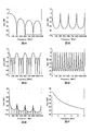
- FIG. 3 shows the various filter characteristics described above.
- the frequency of the local frequency signal LO is 2.4 GHz
- the capacity of the history capacitor 3 is 15 pF
- the capacity of each of the rotation capacitors 4 a to 4 h is 0.5 pF
- the capacity of the buffer capacitor 5 is 15 pF.
- the mutual conductance of the voltage-current converter 1 is set to 7.5 mS.
- FIG. 3A shows the characteristics of the first FIR filter
- FIG. 3B shows the characteristics of the first IIR filter
- 3C shows the characteristics of the second FIR filter
- FIG. 3D shows the characteristics of the second IIR filter
- FIG. 3E shows the characteristics of the entire discrete-time direct sampling circuit
- FIG. 3F is an expanded frequency range in the vicinity of 2.4 GHz among the characteristics of FIG. 3E.
- the DC gain is normalized by 0 dB.
- the discrete-time direct sampling circuit performs the filtering process with the characteristics obtained by combining the characteristics of the first FIR filter, the first IIR filter, the second FIR filter, and the second IIR filter.
- the signal is output to the subsequent circuit.
- An object of the present invention is to provide a direct sampling circuit that avoids signal mixing between systems even when time-sharing integrated signal sequences are used in time division.
- the direct sampling circuit of the present invention includes a switched capacitor filter that filters a signal in which a plurality of input signals are time-integrated and integrated into one system, and is provided for each system in a preceding stage of the switched capacitor filter.
- a history capacitor connected to a rotation capacitor in the switched capacitor filter, a buffer capacitor connected to the rotation capacitor in the switched capacitor filter for each system to be filtered and provided for each system downstream of the switched capacitor filter, and filtered
- a separation unit that separates the signal for each system.
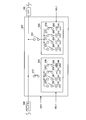
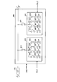
- the figure which shows the structure of the conventional discrete time direct sampling circuit Timing chart for explaining each control signal generated by the digital control unit shown in FIG. Characteristic diagram showing an example of filter characteristics realized by a conventional discrete-time direct sampling circuit The figure which shows the structure of the time division direct sampling mixer which concerns on Embodiment 1 of this invention. The figure which shows the internal structure of the switched capacitor filter shown in FIG. Timing chart for explaining control signals S0 to S3 and selection signals SW1 and SW2 The figure which shows the structure of the time division DSM which concerns on Embodiment 2 of this invention. The figure which shows the internal structure of the history capacitor part which concerns on Embodiment 3 of this invention. The figure which shows the internal structure of the buffer capacitor part which concerns on Embodiment 3 of this invention. The figure which shows the internal structure of the buffer capacitor part which concerns on Embodiment 4 of this invention.
- FIG. 4 is a diagram showing a configuration of a time division direct sampling mixer (hereinafter referred to as “time division DSM (Direct Sampling Mixer)”) 100 according to Embodiment 1 of the present invention.
- time division DSM Direct Sampling Mixer
- the time division integration switch 120 switches between two inputs, an A input for inputting the A system and a B input for inputting the B system, in accordance with the selection signal SW1.
- the time division integration switch 120 time-divisionally integrates the two systems of the A system and the B system into one system signal and outputs it to the transconductance amplifier (TA) 130.
- TA transconductance amplifier
- the transconductance amplifier 130 converts the signal output from the time division integrated switch 120 into a current and outputs the current to the sampler 140.
- the sampler 140 performs sampling processing on the signal output from the transconductance amplifier 130 and down-converts the signal. Sampler 140 outputs the down-converted signal to switched capacitor filter (SCF) 160.
- SCF switched capacitor filter
- Switched capacitor filter 160 receives four control signals S0, S1, S2, and S3 (not shown) and repeats charging and discharging of the rotation capacitor. As a result, the switched capacitor filter 160 performs a filtering process on the signal output from the sampler 140 and outputs the filtered signal to the separation switch 180. Details of the switched capacitor filter 160 will be described later.
- a history capacitor unit 150 is connected between the sampler 140 and the switched capacitor filter 160.
- History capacitors 153 and 155 having different capacities corresponding to the systems are connected to the history capacitor unit 150 via switches 152 and 154, respectively.
- the switches 152 and 154 switch the connection for each system to be processed by the input of the selection signal SW1.
- the selection signal SW1 is the same as the selection signal SW1 input to the time division integration switch 120.
- a buffer capacitor unit 170 is connected between the switched capacitor filter 160 and the separation switch 180.
- Buffer capacitors 173 and 175 having different capacities corresponding to the respective systems are connected to the buffer capacitor unit 170 via switches 172 and 174, respectively.
- the switches 172 and 174 switch the connection for each system to be processed according to the input of the selection signal SW2.
- the selection signal SW2 is a signal obtained by delaying the selection signal SW1 by one time cycle. This is because the output signal of the switched capacitor filter 160 is always delayed by one time cycle with respect to the input signal by the filter processing of the switched capacitor filter 160.
- the separation switch 180 separates the signal output from the switched capacitor filter 160 into each system of A output and B output according to the selection signal SW2. Specifically, when the selection signal SW2 indicates selection of A output, the switch 181 is connected to the input node, and the switch 182 is connected to 0V. On the other hand, when the selection signal SW2 indicates selection of the B output, the switch 182 is connected to the input node, and the switch 181 is connected to 0V.
- the selection signal SW2 is the same as the selection signal SW2 input to the buffer capacitor unit 170.
- the A output from the separation switch 180 is a signal in which the A input subjected to direct sampling processing is zero-padded. From this signal, an aliasing signal generated by system switching is removed by an interpolation filter (not shown) prepared after the separation switch 180, and a signal in a desired band is extracted.
- the B output is processed in the same manner as the A output.
- FIG. 5 is a diagram showing an internal configuration of the switched capacitor filter 160 shown in FIG.
- FIG. 6 is a timing chart of the control signals S0 to S3 and the selection signals SW1 and SW2.
- the operation of the switched capacitor filter 160 will be described with reference to FIGS. 5 and 6.
- a branch from the transistor switch (transistor SW) 240 to the transistor SW244 will be described as an example.
- the selection signal SW1 needs to be synchronized with the control signal, and the length of the high section and the low section needs to be a natural number multiple of the control signal.
- the high section and the low section of the selection signal SW1 are each four time cycles.
- the selection signal SW2 is a signal obtained by delaying the selection signal SW1 by one time cycle.
- time division DSM 100 In the time division DSM 100 according to the present embodiment, a loopback signal due to system switching is generated at the output from the separation switch 180. This folding signal needs to be removed by a filter prepared after the separation switch 180. However, if the operating speed of the selection signal SW1 and the selection signal SW2 is increased, the generation frequency of the folding signal increases. For this reason, the time division DSM 100 can relax the required characteristics of the filter required in the subsequent stage by increasing the operating speed of the selection signal SW1 and the selection signal SW2.
- the IIR filter characteristic realized by the time division DSM 100 is determined by the ratio of the history capacitance Ch included in the history capacitor unit 150 and the rotation capacitor capacitance Cr constituting the switched capacitor filter 160.
- the history capacity Ch is the capacity of the history capacitor 153 or the capacity of the history capacitor 155.
- the rotation capacitor capacitance Cr is any one of the rotation capacitors 221, 231, 241, and 251.
- the IIR filter characteristic realized by the time division DSM 100 is determined by the ratio between the buffer capacitance Cr included in the buffer capacitor 170 and the rotation capacitor capacitance Cr constituting the switched capacitor filter 160.
- the buffer capacity Cr is the capacity of the buffer capacitor 173 or the capacity of the buffer capacitor 175.
- the rotation capacitor capacitance Cr is any one of the rotation capacitors 221, 231, 241, and 251.
- the time division DSM 100 according to the present embodiment is compared with the IIR filter characteristics realized by the general DSM, and the history capacity Ch (153, 155).
- the time division DSM 100 according to the present embodiment can be realized with a buffer capacity Cb (173, 175) having a buffer capacity half that of a general DSM per signal system.
- the total of the history capacity Ch and the total of the buffer capacity Cb that are required is a general DSM. Can be the same size.
- the history capacity Ch and the buffer capacity Cb have a large circuit scale, and these circuits are the most dominant.
- the history capacitor Ch and the buffer capacitor Cb can realize two systems of circuits with the same circuit scale.
- the history capacitor is connected to each system before the switched capacitor filter, the buffer capacitor is connected to each system after the switched capacitor filter, and the rotation of the switched capacitor filter is performed.
- the history capacitor and the buffer capacitor connected to the capacitor are switched for each system for filtering.
- the time division DSM 100 can switch the IIR filter characteristics for each system, so that signal mixing between each system can be avoided and the circuit scale can be reduced.
- one history capacitor and one buffer capacitor are used among the plurality of history capacitors and the plurality of buffer capacitors, respectively, so that power consumption can be reduced.
- the present invention is not limited to this, and one active section of the two systems may be lengthened and the other active section may be shortened.
- the case where one is important data and the other is not important data can be considered. Thereby, the gain can be increased for important data.
- a case where one stream has high performance can be regarded as important data, and a case where the other stream does not have high performance can be regarded as unimportant data.
- FIG. 7 is a diagram showing a configuration of a time division DSM 200 according to Embodiment 2 of the present invention.
- FIG. 7 differs from FIG. 4 in that the buffer capacitor unit 170 is changed to the buffer capacitor unit 270 and the separation switch 180 is changed to the separation switch 280.
- the separation switch 280 separates the signal output from the switched capacitor filter 160 into each system of A output and B output in accordance with the selection signal SW2. Specifically, when the selection signal SW2 indicates selection of the A output, the separation switch 280 is connected to the A output node. On the other hand, when the selection signal SW2 indicates selection of the B output, the separation switch 280 is connected to the B output node.
- the buffer capacitor unit 270 when the separation switch 280 is connected to the A output node, the buffer capacitor 271 is connected to the rotation capacitor of the switched capacitor filter 160. In the buffer capacitor unit 270, the buffer capacitor 272 is connected to the rotation capacitor of the switched capacitor filter 160 when the separation switch 280 is connected to the B output node. In these cases, each of the buffer capacitor units 270 is subjected to IIR filter operation.
- the buffer capacitor on the output node side that is not selected by the separation switch 280 is in a state where electric charge is held, and the output voltage is the voltage that has been selected immediately before.
- the magnitude of the spectrum of the aliasing signal is reduced with reference to the desired wave spectrum included in the A output and the B output.
- the time division DSM 200 can further relax the characteristics required for the filter subsequent to the time division DSM 200.
- the separation capacitor that separates the signals for each system is connected to the switched capacitor filter, and the buffer capacitor is connected to each system after the separation switch.
- the time division DSM 200 can further relax the characteristics required for the filter subsequent to the time division DSM 200 and reduce the number of parts constituting the circuit.
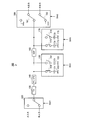
- FIG. 8 is a diagram showing an internal configuration of the history capacitor unit 300 according to the third embodiment of the present invention.
- the history capacitor unit 300 includes a history capacitor group 320 for the first system, a history capacitor group 360 for the second system, and switches 310 and 350 that switch them to conduction or cutoff.
- the switches 310 and 350 can be switched between conduction and interruption exclusively by a selection signal SW1 input from the outside.
- the configuration in the history capacitor group 320 includes N sets of one switch and one history capacitor. Switching between connection and non-connection of these N history capacitors is performed based on a selection signal SEL1.
- the selection signal SEL1 is used for adaptation to various communication systems and fine adjustment of characteristics due to individual variations of system components. Further, the selection signal SEL1 is not changed during a certain communication and is fixed.
- history capacitor group 360 is the same as the history capacitor group 320, a detailed description thereof will be omitted.
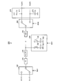
- FIG. 9 is a diagram showing an internal configuration of the buffer capacitor unit 400 according to Embodiment 3 of the present invention.
- the buffer capacitor unit 400 includes a buffer capacitor group 420 for the first system, a buffer capacitor group 460 for the second system, and switches 410 and 450 that switch them to conduction or cutoff.
- the switches 410 and 450 can be switched between conduction and interruption exclusively by a selection signal SW2 input from the outside.
- the buffer capacitor group 420 if one switch and one buffer capacitor are taken as one set, N sets of these are provided. Switching between connection and non-connection of these N buffer capacitors is performed based on a selection signal SEL2. Similar to the selection signal SEL1, the selection signal SEL2 is used for fine adjustment of characteristics and is not changed during a certain communication and is fixed.
- buffer capacitor group 460 is the same as the buffer capacitor group 420, a detailed description thereof will be omitted.
- the time division DSM according to the present embodiment suppresses the deterioration of the filter characteristics due to the addition of the capacitance component to the signal line, and is added directly to the signal line even if the number of history capacitors and buffer capacitors is increased. Capacitance components can be kept small. For this reason, the time division DSM according to the present embodiment can suppress the deterioration of the filter characteristics.
- the time division DSM according to the third embodiment includes a plurality of history capacitors and buffer capacitors connected to the front and rear stages of the switched capacitor filter for each system, and selectively switches between the history capacitors and the buffer capacitors.
- the time division DSM according to the present embodiment can be adapted to various communication systems and finely adjusted characteristics due to individual variations of system components.
- FIG. 10 is a diagram showing an internal configuration of the buffer capacitor unit 500 according to the fourth embodiment of the present invention.
- the buffer capacitor unit 500 includes a buffer capacitor group 520 for the first system and a buffer capacitor group 550 for the second system.
- the configuration in the buffer capacitor group 520 includes N sets of one switch and one buffer capacitor. Switching between connection and non-connection of these N buffer capacitors is performed based on a selection signal SEL3.
- the selection signal SEL3 is used for adaptation to various communication systems and fine adjustment of characteristics due to individual variations of system components. Further, the selection signal SEL3 is not changed during a certain communication and is fixed.
- the buffer capacitor group 550 if one switch and one buffer capacitor are taken as one set, N sets of these are provided. Switching between connection and non-connection of these N buffer capacitors is performed based on a selection signal SEL4. Similar to the selection signal SEL3, the selection signal SEL4 is used for fine adjustment of characteristics, and is not changed during a certain communication and is fixed.
- the separation switch for separating the signal for each system is connected to the switched capacitor filter, and a plurality of buffer capacitors are provided for each system after the separation switch, and the buffer capacitor is selectively used. Switch to.
- the time division DSM according to the present embodiment can further relax the characteristics required for the filter subsequent to the time division DSM.
- the time division DSM according to the present embodiment can be adapted to various communication systems and can finely adjust characteristics due to individual variations of system components.
- the direct sampling circuit according to the present invention is useful as a means for avoiding signal mixing between systems even when time-sharing is used for a time-integrated signal sequence.
Landscapes
- Filters That Use Time-Delay Elements (AREA)
- Analogue/Digital Conversion (AREA)
- Manipulation Of Pulses (AREA)
- Electronic Switches (AREA)
Abstract
時分割統合された信号系列に対して、時分割で兼用する場合であっても、各系統間で信号の混ざりを回避するダイレクトサンプリング回路を提供する。スイッチトキャパシタフィルタ(160)の前段に系統毎にヒストリキャパシタ(153,155)を接続し、スイッチトキャパシタフィルタ(160)の後段に系統毎にバッファキャパシタ(173,175)を接続し、スイッチトキャパシタフィルタ(160)のローテーションキャパシタと接続するヒストリキャパシタ及びバッファキャパシタを入力している時分割系統毎に切り替える。
Description
本発明は、時分割統合された入力信号にダイレクトサンプリング処理を行うダイレクトサンプリング回路に関する。
無線受信機の小型低消費電力化やアナログ信号処理部とデジタル信号処理部の一体化を目指すため、高周波信号を直接離散時間的にサンプリングして受信処理する構成が開示されている(例えば、特許文献1参照)。
以下、図1を用いて、従来の離散時間的処理を用いた離散時間ダイレクトサンプリング回路の構成と動作の一例について説明する。図1は全体として、離散時間ダイレクトサンプリング回路を示す。離散時間ダイレクトサンプリング回路は、電圧電流変換器(TA)1と、サンプリングスイッチ2と、ヒストリキャパシタ(CH)3と、ローテーションキャパシタ群4a~4hと、バッファキャパシタ(CB)5と、ダンプスイッチ6と、リセットスイッチ7と、積分スイッチ群8a~8hと、放出スイッチ群9a~9hと、デジタルコントロールユニット10とを備えている。
電圧電流変換器(TA)1は、受信した無線周波数(RF)信号を電流に変換し、アナログRF電流信号として出力する。サンプリングスイッチ2は、例えばFETで構成され、ローカル周波数信号入力(LO)に応じて、入力されるアナログRF電流信号をサンプリングする。
ヒストリキャパシタ(CH)3は、サンプリングスイッチ2から出力される電流により供給される電荷を充電する。ローテーションキャパシタ群4a~4hは、複数種類のスイッチを介してヒストリキャパシタ3とバッファキャパシタ5と並列に接続されている。また、ローテーションキャパシタ群4a~4hは、各々のスイッチのオン、オフ制御に応じて電荷の充電もしくは放電をする複数のローテーションキャパシタ(CR)により構成されている。
バッファキャパシタ(CB)5は、複数のローテーションキャパシタ4に充電されている電荷と共有接続され、電荷信号をバッファする。ダンプスイッチ6は、ローテーションキャパシタ群4a~4hの各々とバッファキャパシタ5の接続をオン、オフする。リセットスイッチ7は、バッファキャパシタ5と電荷共有した後で、ローテーションキャパシタ4に蓄えられている電荷を接地する。
積分スイッチ群8a~8hは、複数の積分スイッチにより構成されている。また、積分スイッチ群8a~8hは、ヒストリキャパシタ3とローテーションキャパシタ群4a~4hにおける各々のローテーションキャパシタとの接続をオン、オフする。放出スイッチ群9a~9hは、複数の放出スイッチにより構成されている。また、放出スイッチ群9a~9hは、ローテーションキャパシタ群4a~4hにおける各々のローテーションキャパシタとバッファキャパシタ5との接続をオン、オフする。
ダンプスイッチ6、リセットスイッチ7、積分スイッチ群8a~8h及び放出スイッチ群9a~9hは、例えばFET(n型)で構成されている。n型FETは、ゲート電圧が高い状態(ハイ)でオン(導通)し、ゲート電圧が低い状態(ロー)でオフ(遮断)する。
デジタルコントロールユニット10は、積分スイッチ群8a~8h、放出スイッチ群9a~9h、ダンプスイッチ6及びリセットスイッチ7に対して制御信号を生成して供給する。
なお、ここでは一例として、離散時間ダイレクトサンプリング回路にローテーションキャパシタCRが8個設けられた場合を仮定している。これに応じて、積分スイッチ8a~8h、放出スイッチ9a~9hは、それぞれ8個設けられているものとする。そして、それぞれの構成要素の付番の末尾には、アルファベット順にa~hを付している。また、実際には、離散時間ダイレクトサンプリング回路が差動動作をする構成とすることも可能であり、その構成は特許文献1で開示されている。しかしながら、ここでは簡単化のために説明を割愛する。
図2は、デジタルコントロールユニット10が生成する各制御信号のタイミングチャートを示す。ローカル周波数信号(LO)は、サンプリングスイッチ2のゲートに供給される。制御信号S1~S8は、それぞれ積分スイッチ8a~8hのゲートに供給される。制御信号SAZは、放出スイッチ9a~9dのゲートに供給される。制御信号SBZは、放出スイッチ9e~9hのゲートに供給される。制御信号Dはダンプスイッチ6のゲートに、制御信号Rはリセットスイッチ7のゲートにそれぞれ供給される。
以下、図1に示す離散時間ダイレクトサンプリング回路の動作について説明する。電圧電流変換器1は、入力されたアナログRF信号をアナログRF電流信号に変換し、サンプリングスイッチ2に出力する。アナログRF電流信号は、サンプリングスイッチ2でアナログRF電流信号とほぼ同じ周波数を持ったローカル周波数信号LOでサンプリングされる。ローカル周波数信号LOでサンプリングされた信号は、ヒストリキャパシタ3とローテーションキャパシタ4a~4hによって電荷が積分されることにより、時間的に離散化された離散信号とされる。
ヒストリキャパシタ3とローテーションキャパシタ群4a~4hのうちの一つとにより並列接続状態のキャパシタが構成される。このように構成されたキャパシタによって、離散信号はローカル周波数信号LOのクロック長よりも長い時間に亘って積分される。これにより、フィルタ処理とデシメーション(decimation:間引き)が行われる。
具体的には、離散時間ダイレクトサンプリング回路では、初めに、制御信号S1により積分スイッチ8aがオンし、ローテーションキャパシタ4aがヒストリキャパシタ3と接続される。そして、制御信号S1がハイになっている期間(例えば、ローカル周波数信号LOの8周期分)に亘って前記2つのキャパシタに供給された電荷が積分される。
制御信号S1がローになると、ヒストリキャパシタ3は、ローテーションキャパシタ4aとの接続がオフとなり、制御信号S2によりローテーションキャパシタ4bとの接続がオンとなる。ローテーションキャパシタ4bは、制御信号S2がハイの期間に亘って離散信号の電流により供給される電荷を積分した後、ヒストリキャパシタ3との接続をオフする。同様にして、ローテーションキャパシタ4c~4hは、制御信号S3~S8により、ローカル周波数信号LOの8周期ごとに順番にヒストリキャパシタ3と接続される。そして、2つのキャパシタによって離散信号の電流により供給される電荷が積分される。
このようにして、離散時間ダイレクトサンプリング回路では、ローカル周波数信号LOの8周期分の離散信号の電流により供給される電荷を積分する。これにより、離散時間ダイレクトサンプリング回路では、8タップのFIR(Finite Impulse Response)フィルタの特性が実現される。また、ローカル周波数信号LOの8周期分の信号を積分することによって1サンプル分の電荷量が得られるため、サンプリングレートは1/8にデシメーションされる。このフィルタ特性を実現する機能部は、第1のFIRフィルタと呼ぶことにする。
また、離散時間ダイレクトサンプリング回路では、ヒストリキャパシタ3にローテーションキャパシタ4a~4hが順に接続されることで、IIR(Infinite Impulse Response)フィルタの特性が実現される。このフィルタ特性を実現する機能部は、第1のIIRフィルタと呼ぶことにする。
次に、制御信号SAZにより放出スイッチ9a~9dが、オンされることによって、ローテーションキャパシタ4a~4dとバッファキャパシタ5とが導通される。これにより、ローテーションキャパシタ4a~4dに充電された電荷は、バッファキャパシタ5との間で共有される。この結果、ローテーションキャパシタ4a~4dのそれぞれの電荷の一部は、バッファキャパシタ5に移動し、電荷量が合成される。
ローテーションキャパシタ4a~4dとバッファキャパシタ5との間の電荷共有の後、ダンプスイッチ6は、制御信号Dによりオフとされ、電荷共有状態が解消される。次に、制御信号Rによりリセットスイッチ7がオンとされ、ローテーションキャパシタ4a~4dに残っていた電荷は、接地によりリセットされる。
このようにして、離散時間ダイレクトサンプリング回路では、ローテーションキャパシタ4a~4dの各々に充電された電荷の一部をバッファキャパシタ5に移動して合成することで、4タップのFIRフィルタの特性が実現される。離散時間ダイレクトサンプリング回路では、4サンプル分の離散信号が合成されて1サンプル分の離散信号が出力されるため、サンプリングレートは、1/4にデシメーションされる。
ローテーションキャパシタ4e~4hも同じように、制御信号SBZにより放出スイッチ9e~9hがオンされ、それぞれのローテーションキャパシタに充電されている電荷の一部は、バッファキャパシタ5との間で共有される。これにより、離散時間ダイレクトサンプリング回路では、4タップのFIRフィルタ処理と1/4デシメーションが行われる。このフィルタ特性は、第2のFIRフィルタと呼ぶことにする。
また、離散時間ダイレクトサンプリング回路では、ローテーションキャパシタ4a~4d及び4e~4hの各グループを、バッファキャパシタ5と交互に電荷共有状態にすることで、IIRフィルタ特性が実現される。このフィルタ特性は、第2のIIRフィルタと呼ぶことにする。
図3は、上記の各種フィルタ特性を示す。ここでは、ローカル周波数信号LOの周波数を2.4GHz、ヒストリキャパシタ3の容量を15pF、ローテーションキャパシタ4a~4hの各々の容量を0.5pF、バッファキャパシタ5の容量を15pFとする。また、電圧電流変換器1の相互コンダクタンスを7.5mSとする。
図3Aは第1のFIRフィルタの特性、図3Bは第1のIIRフィルタの特性を示す。また、図3Cは第2のFIRフィルタの特性、図3Dは第2のIIRフィルタの特性を示す。さらに、図3Eは離散時間ダイレクトサンプリング回路全体の特性を示しており、図3Fは図3Eの特性のうち2.4GHz近傍の周波数範囲を拡大したものである。なお、図において、DC利得は、0dBで正規化している。
以上のように、離散時間ダイレクトサンプリング回路は、第1のFIRフィルタ、第1のIIRフィルタ、第2のFIRフィルタ、および第2のIIRフィルタの各特性を、合わせた特性のフィルタ処理を施した信号を、後段の回路に出力する。
ところで、近年、MIMO(Multiple Input Multiple Output)、MRC(Maximum Ratio Combining)及びダイバーシティなどのシステムは、複数の高周波部を必要とする。このようなシステムでは、回路規模を削減するために高周波部を時分割使用し、回路を兼用することが要求されている。
しかしながら、図1で示したような従来のダイレクトサンプリング回路では、回路の時分割兼用を考えた場合、一般に、時分割統合された信号に対して、フィルタ効果のあるオペレーションを実施すると、次のような課題がある。すなわち、従来のダイレクトサンプリング回路では、各系統間で信号の混ざりが発生し、その出力を各系統に分離することが困難になる。また、IIRフィルタ効果を有するダイレクトサンプリング回路は、時分割統合された信号を処理した場合、各系統間で信号が混ざり、所望のダイレクトサンプリング演算を実施することが困難になる。
本発明の目的は、時分割統合された信号系列に対して、時分割で兼用する場合であっても、各系統間で信号の混ざりを回避するダイレクトサンプリング回路を提供することである。
本発明のダイレクトサンプリング回路は、複数系統の入力信号が1系統に時分割統合された信号をフィルタリングするスイッチトキャパシタフィルタと、前記スイッチトキャパシタフィルタの前段に系統毎に設けられ、フィルタリングする系統毎に前記スイッチトキャパシタフィルタ内のローテーションキャパシタと接続するヒストリキャパシタと、前記スイッチトキャパシタフィルタの後段に系統毎に設けられ、フィルタリングする系統毎に前記スイッチトキャパシタフィルタ内のローテーションキャパシタと接続するバッファキャパシタと、フィルタリングされた前記信号を系統毎に分離する分離部と、を具備する構成を採る。
本発明によれば、時分割統合された信号系列に対して、時分割で兼用する場合であっても、各系統間で信号の混ざりを回避することができる。
以下、本発明の実施の形態について、図面を参照して詳細に説明する。ただし、実施の形態において、同一機能を有する構成には、同一符号を付し、重複する説明は省略する。
(実施の形態1)
図4は、本発明の実施の形態1に係る時分割ダイレクトサンプリングミキサ(以下、「時分割DSM(Direct Sampling Mixer)」という)100の構成を示す図である。以下、時分割DSM100の構成について図4を用いて説明する。
図4は、本発明の実施の形態1に係る時分割ダイレクトサンプリングミキサ(以下、「時分割DSM(Direct Sampling Mixer)」という)100の構成を示す図である。以下、時分割DSM100の構成について図4を用いて説明する。
時分割統合スイッチ120は、選択信号SW1に従って、A系統を入力するA入力とB系統を入力するB入力の2つの入力を切り替える。これにより、時分割統合スイッチ120は、A系統とB系統の2系統を1系統信号に時分割統合して、トランスコンダクタンスアンプ(TA)130に出力する。
トランスコンダクタンスアンプ130は、時分割統合スイッチ120から出力された信号を電流に変換して、サンプラ140に出力する。サンプラ140は、トランスコンダクタンスアンプ130から出力された信号にサンプリング処理を施して、ダウンコンバートする。サンプラ140は、ダウンコンバートした信号をスイッチトキャパシタフィルタ(SCF)160に出力する。
スイッチトキャパシタフィルタ160は、図示せぬ4つの制御信号S0,S1,S2,S3の入力を受けて、ローテーションキャパシタの充放電を繰り返す。これにより、スイッチトキャパシタフィルタ160は、サンプラ140から出力された信号にフィルタ処理を施して、分離スイッチ180に出力する。なお、スイッチトキャパシタフィルタ160の詳細については後述する。
サンプラ140とスイッチトキャパシタフィルタ160との間には、ヒストリキャパシタ部150が接続されている。ヒストリキャパシタ部150には、系統毎に対応した容量の異なるヒストリキャパシタ153,155がそれぞれスイッチ152,154を介して接続されている。スイッチ152,154は、選択信号SW1の入力によって処理する系統毎に接続を切り替える。なお、この選択信号SW1は、時分割統合スイッチ120に入力される選択信号SW1と同一である。
また、スイッチトキャパシタフィルタ160と分離スイッチ180との間には、バッファキャパシタ部170が接続されている。バッファキャパシタ部170には、系統毎に対応した容量の異なるバッファキャパシタ173,175がそれぞれスイッチ172,174を介して接続されている。スイッチ172,174は、選択信号SW2の入力によって処理する系統毎に接続を切り替える。
この選択信号SW2は、選択信号SW1を1タイムサイクル遅延させた信号である。これは、スイッチトキャパシタフィルタ160の出力信号が、スイッチトキャパシタフィルタ160のフィルタ処理によって入力信号に対して常に1タイムサイクル遅延するためである。
分離スイッチ180は、選択信号SW2に従って、スイッチトキャパシタフィルタ160から出力された信号をA出力とB出力の各系統に分離する。具体的には、選択信号SW2がA出力の選択を示している場合、スイッチ181が入力ノードと接続され、スイッチ182が0Vと接続される。一方、選択信号SW2がB出力の選択を示している場合、スイッチ182が入力ノードと接続され、スイッチ181が0Vと接続される。なお、選択信号SW2は、バッファキャパシタ部170に入力される選択信号SW2と同一である。
分離スイッチ180からのA出力は、ダイレクトサンプリング処理が施されたA入力がゼロパディングされた信号となる。この信号は、分離スイッチ180の後段に用意された図示せぬ補間フィルタによって、系統切り替えによって生じる信号の折り返し信号が除去され、所望の帯域の信号が抽出される。B出力は、A出力と同様に処理される。
図5は、図4に示したスイッチトキャパシタフィルタ160の内部構成を示す図である。また、図6は、制御信号S0~S3及び選択信号SW1,SW2のタイミングチャートを示す図である。以下、図5及び図6を用いて、スイッチトキャパシタフィルタ160の動作について説明する。ここでは、トランジスタスイッチ(トランジスタSW)240~トランジスタSW244までのブランチを例に説明する。
時刻T0では、制御信号S0だけがハイになることによって、トランジスタSW242が導通する。これにより、ローテーションキャパシタ241に充電されている電荷は、全て放電される。
時刻T1では、制御信号S1だけがハイになることによって、トランジスタSW243が導通する。これにより、プリチャージ電圧からローテーションキャパシタ241には、初期電荷が充電される。
時刻T2では、制御信号S2だけがハイになることによって、トランジスタSW240が導通する。これにより、スイッチトキャパシタフィルタ160の前段にあるヒストリキャパシタ153又は155と、ローテーションキャパシタ241とが並列接続される。その結果、1タイムサイクル前の初期電荷と、接続されているヒストリ容量Ch及びローテーション容量Crの容量比に応じた電荷とを加算した電荷は、ローテーションキャパシタ241に充電される。
時刻T3では、制御信号S3だけがハイになることによって、トランジスタSW244が導通する。これにより、スイッチトキャパシタフィルタ160の後段にあるバッファキャパシタ173又は175と、ローテーションキャパシタ241とが並列接続される。その結果、接続されているバッファ容量Cbとローテーション容量Crの容量比に応じた電荷は、ローテーションキャパシタ241に充電される。時刻T4以降では、時刻T0~T3の処理が繰り返される。
トランジスタSW220~トランジスタSW224のブランチ、トランジスタSW230~トランジスタSW234のブランチ、トランジスタSW250~トランジスタSW254のブランチは、タイムステップをずらしながら同様の処理がなされる。
このように、スイッチトキャパシタフィルタ160前段のヒストリキャパシタ部150と、スイッチトキャパシタフィルタ160内のローテーションキャパシタとの間では、電荷共有を行う。これにより、スイッチトキャパシタフィルタ160は、IIRフィルタ操作が行われる。同様に、スイッチトキャパシタフィルタ160後段のバッファキャパシタ部170と、スイッチトキャパシタフィルタ160内のローテーションキャパシタとの間では、電荷共有を行う。これにより、スイッチトキャパシタフィルタ160は、IIRフィルタ操作が行われる。この結果、スイッチトキャパシタフィルタ160は、2次のIIRフィルタを形成することになる。
なお、選択信号SW1は、図6に示すように、制御信号と同期している必要があり、ハイ区間及びロー区間の長さは制御信号の自然数倍である必要がある。ここでは、選択信号SW1のハイ区間及びロー区間は、それぞれ4タイムサイクルである。選択信号SW2は、上述したように、選択信号SW1を1タイムサイクル遅延させた信号である。
本実施の形態に係る時分割DSM100では、分離スイッチ180からの出力において、系統切り替えによる折り返し信号が発生する。この折り返し信号は、分離スイッチ180の後段に用意するフィルタで除去する必要がある。ところが、選択信号SW1と選択信号SW2の動作速度を高速にすれば、折り返し信号の発生周波数が大きくなる。このため、時分割DSM100は、選択信号SW1と選択信号SW2の動作速度を高速にすることにより、後段に必要となるフィルタの要求特性を緩くすることができる。
このように、時分割DSM100で実現されるIIRフィルタ特性は、ヒストリキャパシタ部150に含まれるヒストリ容量Chと、スイッチトキャパシタフィルタ160を構成するローテーションキャパシタ容量Crとの比により決定される。なお、ヒストリ容量Chは、ヒストリキャパシタ153の容量又はヒストリキャパシタ155の容量である。なお、ローテーションキャパシタ容量Crは、ローテーションキャパシタ221、231、241、251のいずれかの容量Crである。または、時分割DSM100で実現されるIIRフィルタ特性は、バッファキャパシタ170に含まれるバッファ容量Crと、スイッチトキャパシタフィルタ160を構成するローテーションキャパシタ容量Crとの比により決定される。なお、バッファ容量Crは、バッファキャパシタ173の容量又はバッファキャパシタ175の容量である。なお、ローテーションキャパシタ容量Crは、ローテーションキャパシタ221、231、241、251のいずれかの容量Crである。
これにより、本実施の形態に係る時分割DSM100は、一般的なDSMによって実現されるIIRフィルタ特性と比較し、1つの信号系統当たり、一般的なDSMの半分の容量のヒストリ容量Ch(153、155)で実現することができる。同様に、本実施の形態に係る時分割DSM100は、バッファ容量も1つの信号系統当たり、一般的なDSMの半分の容量のバッファ容量Cb(173、175)で実現することができる。つまり、2系統を時分割使用する時分割DSMにおいて、一般的なDSMと同等のIIRフィルタ効果を実現するために、必要となるヒストリ容量Chの総和とバッファ容量Cbの総和は、一般的なDSMと同じ大きさで済ませることができる。
一般的なDSMにおいては、ヒストリ容量Chとバッファ容量Cbは回路規模が大きく、これらの回路が最も支配的である。これに対して、本実施の形態に係る時分割統合DSM100では、ヒストリ容量Chとバッファ容量Cbとは、同等の回路規模で、2系統の回路を実現することができる。
このように、実施の形態1に係る時分割DSM100は、スイッチトキャパシタフィルタの前段に系統毎にヒストリキャパシタを接続し、スイッチトキャパシタフィルタの後段に系統毎にバッファキャパシタを接続し、スイッチトキャパシタフィルタのローテーションキャパシタと接続するヒストリキャパシタ及びバッファキャパシタをフィルタリングする系統毎に切り替える。これにより、時分割DSM100は、系統毎にIIRフィルタ特性を切り替えることができるので、各系統間で信号の混ざりを回避することができると共に、回路規模を削減することができる。
また、時分割DSM100は、複数のヒストリキャパシタ及び複数のバッファキャパシタのうち、それぞれ1つのヒストリキャパシタ及び1つのバッファキャパシタが用いられるので、消費電力を低減することができる。
なお、本実施の形態では、A系統とB系統の2系統に対してIIRフィルタ操作がかかるアクティブ区間が同一である場合について説明した。しかしながら、本発明は、これに限らず、2系統のうち一方のアクティブ区間を長くし、他方のアクティブ区間を短くしてもよい。これは、例えば、一方を重要なデータとし、他方を重要ではないデータとした場合が考えられる。これにより、重要なデータについては、ゲインを増やすことができる。このようなデータの例として、2ストリームのダイバーシティでは、一方のストリームが高性能である場合を重要なデータ、他方のストリームが高性能ではない場合を重要ではないデータと考えることができる。
(実施の形態2)
図7は、本発明の実施の形態2に係る時分割DSM200の構成を示す図である。図7が図4と異なる点は、バッファキャパシタ部170をバッファキャパシタ部270に変更し、分離スイッチ180を分離スイッチ280に変更した点である。
図7は、本発明の実施の形態2に係る時分割DSM200の構成を示す図である。図7が図4と異なる点は、バッファキャパシタ部170をバッファキャパシタ部270に変更し、分離スイッチ180を分離スイッチ280に変更した点である。
分離スイッチ280は、選択信号SW2に従って、スイッチトキャパシタフィルタ160から出力された信号をA出力とB出力の各系統に分離する。具体的には、選択信号SW2がA出力の選択を示している場合、分離スイッチ280がA出力ノードと接続される。一方、選択信号SW2がB出力の選択を示している場合、分離スイッチ280は、B出力ノードと接続される。
バッファキャパシタ部270は、分離スイッチ280がA出力ノードと接続されたとき、バッファキャパシタ271がスイッチトキャパシタフィルタ160のローテーションキャパシタと接続される。また、バッファキャパシタ部270は、分離スイッチ280がB出力ノードと接続されたとき、バッファキャパシタ272がスイッチトキャパシタフィルタ160のローテーションキャパシタと接続される。これらの場合において、バッファキャパシタ部270は、それぞれIIRフィルタ操作が行われる。
このような構成により、分離スイッチ280において選択されていない出力ノード側のバッファキャパシタには、電荷が保持された状態となり、出力電圧は直前に選択された状態の電圧となる。この結果、A出力とB出力に含まれる所望波スペクトルを基準として折り返し信号のスペクトルの大きさが小さくなる。このため、時分割DSM200は、時分割DSM200後段のフィルタに要求される特性をさらに緩和することができる。
このように、実施の形態2に係る時分割DSM200は、スイッチトキャパシタフィルタに系統毎の信号に分離する分離スイッチを接続し、分離スイッチ後段にバッファキャパシタを系統毎に接続する。これにより、時分割DSM200は、時分割DSM200後段のフィルタに要求される特性をさらに緩和し、回路を構成する部品点数を減らすことができる。
(実施の形態3)
本発明の実施の形態3に係る時分割DSMの構成は、実施の形態1の図4に示した構成と同様であり、ヒストリキャパシタ部とバッファキャパシタ部の内部構成が異なるのみである。
本発明の実施の形態3に係る時分割DSMの構成は、実施の形態1の図4に示した構成と同様であり、ヒストリキャパシタ部とバッファキャパシタ部の内部構成が異なるのみである。
図8は、本発明の実施の形態3に係るヒストリキャパシタ部300の内部構成を示す図である。以下、ヒストリキャパシタ部300の構成について図8を用いて説明する。ヒストリキャパシタ部300は、1つ目の系統用のヒストリキャパシタ群320と、2つ目の系統用のヒストリキャパシタ群360と、それらを導通又は遮断に切り替えるスイッチ310、350から構成される。
スイッチ310、350は、外部から入力される選択信号SW1によって互いに排他的に導通と遮断とを切り替えられる。
ヒストリキャパシタ群320内の構成は、1つのスイッチと1つのヒストリキャパシタとを1組とすると、これらがN組み設けられている。これらN個のヒストリキャパシタの接続と非接続との切り替えは、選択信号SEL1に基づいて行われる。選択信号SEL1は、さまざまな通信システムへの適応や、システム構成要素の個体ばらつきなどによる特性の微調整に用いられる。また、選択信号SEL1は、ある一つの通信時には変更されず固定である。
ヒストリキャパシタ群360は、ヒストリキャパシタ群320と同様であるので、その詳細な説明は省略する。
図9は、本発明の実施の形態3に係るバッファキャパシタ部400の内部構成を示す図である。以下、バッファキャパシタ部400の構成について図9を用いて説明する。バッファキャパシタ部400は、1つ目の系統用のバッファキャパシタ群420と、2つ目の系統用のバッファキャパシタ群460と、それらを導通又は遮断に切り替えるスイッチ410、450から構成される。
スイッチ410、450は、外部から入力される選択信号SW2によって互いに排他的に導通と遮断とを切り替えられる。
バッファキャパシタ群420内の構成は、1つのスイッチと1つのバッファキャパシタとを1組とすると、これらがN組み設けられている。これらN個のバッファキャパシタの接続と非接続との切り替えは、選択信号SEL2に基づいて行われる。選択信号SEL2は、選択信号SEL1と同様、特性の微調整に用いられ、ある一つの通信時には変更されず固定である。
バッファキャパシタ群460は、バッファキャパシタ群420と同様であるので、その詳細な説明は省略する。
本実施の形態に係る時分割DSMは、信号線に容量成分が付加されることによる、フィルタ特性の劣化を抑制し、ヒストリキャパシタ及びバッファキャパシタの個数を増加させても信号線に直接付加される容量成分を小さく抑えることができる。このため、本実施の形態に係る時分割DSMは、フィルタ特性の劣化を抑えることができる。
このように、実施の形態3に係る時分割DSMは、スイッチトキャパシタフィルタの前段及び後段に接続するヒストリキャパシタ及びバッファキャパシタを系統毎に複数備え、ヒストリキャパシタ及びバッファキャパシタを選択的に切り替える。これにより、本実施の形態に係る時分割DSMは、さまざまな通信システムへの適応、また、システム構成要素の個体ばらつきなどによる特性の微調整を行うことができる。
(実施の形態4)
本発明の実施の形態4に係る時分割DSMの構成は、実施の形態2の図7に示した構成と同様であり、バッファキャパシタ部の内部構成が異なるのみである。
本発明の実施の形態4に係る時分割DSMの構成は、実施の形態2の図7に示した構成と同様であり、バッファキャパシタ部の内部構成が異なるのみである。
図10は、本発明の実施の形態4に係るバッファキャパシタ部500の内部構成を示す図である。以下、バッファキャパシタ部500の構成について図10を用いて説明する。バッファキャパシタ部500は、1つ目の系統用のバッファキャパシタ群520と、2つ目の系統用のバッファキャパシタ群550とから構成される。
バッファキャパシタ群520内の構成は、1つのスイッチと1つのバッファキャパシタとを1組とすると、これらがN組み設けられている。これらN個のバッファキャパシタの接続と非接続との切り替えは、選択信号SEL3に基づいて行われる。選択信号SEL3は、さまざまな通信システムへの適応や、システム構成要素の個体ばらつきなどによる特性の微調整に用いられる。また、選択信号SEL3は、ある一つの通信時には変更されず固定である。
バッファキャパシタ群550内の構成は、1つのスイッチと1つのバッファキャパシタとを1組とすると、これらがN組み設けられている。これらN個のバッファキャパシタの接続と非接続との切り替えは、選択信号SEL4に基づいて行われる。選択信号SEL4は、選択信号SEL3と同様、特性の微調整に用いられ、ある一つの通信時には変更されず固定である。
このように、実施の形態4に係る時分割DSMは、スイッチトキャパシタフィルタに系統毎の信号に分離する分離スイッチを接続し、分離スイッチ後段にバッファキャパシタを系統毎に複数備え、バッファキャパシタを選択的に切り替える。これにより、本実施の形態に係る時分割DSMは、時分割DSM後段のフィルタに要求される特性をさらに緩和することができる。また、本実施の形態に係る時分割DSMは、さまざまな通信システムへの適応、また、システム構成要素の個体ばらつきなどによる特性の微調整を行うことができる。
2010年7月15日出願の特願2010-160721の日本出願に含まれる明細書、図面及び要約書の開示内容は、すべて本願に援用される。
本発明にかかるダイレクトサンプリング回路は、時分割統合された信号系列に対して、時分割で兼用する場合であっても、各系統間で信号の混ざりを回避するものとして有用である。
120 時分割統合スイッチ
130 トランスコンダクタンスアンプ
140 サンプラ
150、300 ヒストリキャパシタ部
152、154、172、174、181、182、310、330、331、332、339、350、370、371、372、379、410、430、431、432、439、450、470、471、472、479、530、531、532、539、560、561、562、569 スイッチ
153、155、340、341、342、349、380、381、382、389 ヒストリキャパシタ
160 スイッチトキャパシタフィルタ
170、270、400、500 バッファキャパシタ部
173、175、271、272、440、441、442、449、480、481、482、489、540、541、542、549、570、571、572、579 バッファキャパシタ
180、280 分離スイッチ
220、222、223、224、230、232、233、234、240、242、243、244、250、252,253、254 トランジスタスイッチ
221、231、241、251 ローテーションキャパシタ
320、360 ヒストリキャパシタ群
420、460、520、550 バッファキャパシタ群
130 トランスコンダクタンスアンプ
140 サンプラ
150、300 ヒストリキャパシタ部
152、154、172、174、181、182、310、330、331、332、339、350、370、371、372、379、410、430、431、432、439、450、470、471、472、479、530、531、532、539、560、561、562、569 スイッチ
153、155、340、341、342、349、380、381、382、389 ヒストリキャパシタ
160 スイッチトキャパシタフィルタ
170、270、400、500 バッファキャパシタ部
173、175、271、272、440、441、442、449、480、481、482、489、540、541、542、549、570、571、572、579 バッファキャパシタ
180、280 分離スイッチ
220、222、223、224、230、232、233、234、240、242、243、244、250、252,253、254 トランジスタスイッチ
221、231、241、251 ローテーションキャパシタ
320、360 ヒストリキャパシタ群
420、460、520、550 バッファキャパシタ群
Claims (4)
- 複数系統の入力信号が1系統に時分割統合された信号をフィルタリングするスイッチトキャパシタフィルタと、
前記スイッチトキャパシタフィルタの前段に系統毎に設けられ、フィルタリングする系統毎に前記スイッチトキャパシタフィルタ内のローテーションキャパシタと接続するヒストリキャパシタと、
前記スイッチトキャパシタフィルタの後段に系統毎に設けられ、フィルタリングする系統毎に前記スイッチトキャパシタフィルタ内のローテーションキャパシタと接続するバッファキャパシタと、
フィルタリングされた前記信号を系統毎に分離する分離部と、
を具備するダイレクトサンプリング回路。 - 前記バッファキャパシタは、前記分離部の後段に設けられた請求項1に記載のダイレクトサンプリング回路。
- 前記ヒストリキャパシタ及び前記バッファキャパシタは、系統毎にそれぞれ複数設けられ、選択的に接続を切り替えられる請求項1に記載のダイレクトサンプリング回路。
- 前記バッファキャパシタは、系統毎に複数設けられ、選択的に接続を切り替えられる請求項2に記載のダイレクトサンプリング回路。
Priority Applications (1)
| Application Number | Priority Date | Filing Date | Title |
|---|---|---|---|
| US13/805,842 US8836378B2 (en) | 2010-07-15 | 2011-06-29 | Direct sampling circuit |
Applications Claiming Priority (2)
| Application Number | Priority Date | Filing Date | Title |
|---|---|---|---|
| JP2010160721A JP5393607B2 (ja) | 2010-07-15 | 2010-07-15 | ダイレクトサンプリング回路 |
| JP2010-160721 | 2010-07-15 |
Publications (1)
| Publication Number | Publication Date |
|---|---|
| WO2012008106A1 true WO2012008106A1 (ja) | 2012-01-19 |
Family
ID=45469126
Family Applications (1)
| Application Number | Title | Priority Date | Filing Date |
|---|---|---|---|
| PCT/JP2011/003709 Ceased WO2012008106A1 (ja) | 2010-07-15 | 2011-06-29 | ダイレクトサンプリング回路 |
Country Status (3)
| Country | Link |
|---|---|
| US (1) | US8836378B2 (ja) |
| JP (1) | JP5393607B2 (ja) |
| WO (1) | WO2012008106A1 (ja) |
Families Citing this family (2)
| Publication number | Priority date | Publication date | Assignee | Title |
|---|---|---|---|---|
| WO2016034242A1 (en) * | 2014-09-05 | 2016-03-10 | Huawei Technologies Co., Ltd. | A charge sharing filter |
| EP4175117A4 (en) * | 2020-06-26 | 2023-08-02 | Terawatt Technology K.K. | BATTERY SYSTEM, CONTROL DEVICE AND CONTROL METHOD |
Citations (3)
| Publication number | Priority date | Publication date | Assignee | Title |
|---|---|---|---|---|
| JPH07249989A (ja) * | 1994-03-11 | 1995-09-26 | Yamaha Corp | アナログ/ディジタル変換器 |
| JPH0983301A (ja) * | 1995-09-07 | 1997-03-28 | Yamaha Corp | スイッチドキャパシタフィルタ |
| WO2009004818A1 (ja) * | 2007-07-05 | 2009-01-08 | Panasonic Corporation | 離散フィルタ、サンプリングミキサ及び無線装置 |
Family Cites Families (9)
| Publication number | Priority date | Publication date | Assignee | Title |
|---|---|---|---|---|
| JPS5678895A (en) * | 1979-11-30 | 1981-06-29 | Nippon Hamondo Kk | Multiplex sounddsource signal forming device for electronic musical instrument |
| JP3272438B2 (ja) * | 1993-02-01 | 2002-04-08 | 芳男 山崎 | 信号処理システムおよび処理方法 |
| US8027657B2 (en) | 2001-10-26 | 2011-09-27 | Texas Instruments Incorporated | Sampling mixer with asynchronous clock and signal domains |
| US7982533B2 (en) * | 2005-08-22 | 2011-07-19 | Mediatek Usa Inc. | Transceiving system and compound filter |
| JP5046622B2 (ja) * | 2005-12-13 | 2012-10-10 | パナソニック株式会社 | サンプリングフィルタ装置 |
| JP5019313B2 (ja) * | 2006-03-07 | 2012-09-05 | パナソニック株式会社 | 離散時間ダイレクトサンプリング回路及び受信機 |
| US7439898B1 (en) | 2007-05-31 | 2008-10-21 | Analog Devices, Inc. | Parallel digital processing for reducing delay in SAR ADC logic |
| JP4954150B2 (ja) | 2007-07-05 | 2012-06-13 | パナソニック株式会社 | 離散フィルタ、サンプリングミキサ及び無線装置 |
| WO2009075105A1 (ja) * | 2007-12-12 | 2009-06-18 | Panasonic Corporation | サンプリングミキサ、直交復調器、及び無線装置 |
-
2010
- 2010-07-15 JP JP2010160721A patent/JP5393607B2/ja not_active Expired - Fee Related
-
2011
- 2011-06-29 WO PCT/JP2011/003709 patent/WO2012008106A1/ja not_active Ceased
- 2011-06-29 US US13/805,842 patent/US8836378B2/en not_active Expired - Fee Related
Patent Citations (3)
| Publication number | Priority date | Publication date | Assignee | Title |
|---|---|---|---|---|
| JPH07249989A (ja) * | 1994-03-11 | 1995-09-26 | Yamaha Corp | アナログ/ディジタル変換器 |
| JPH0983301A (ja) * | 1995-09-07 | 1997-03-28 | Yamaha Corp | スイッチドキャパシタフィルタ |
| WO2009004818A1 (ja) * | 2007-07-05 | 2009-01-08 | Panasonic Corporation | 離散フィルタ、サンプリングミキサ及び無線装置 |
Also Published As
| Publication number | Publication date |
|---|---|
| JP5393607B2 (ja) | 2014-01-22 |
| US20130099828A1 (en) | 2013-04-25 |
| US8836378B2 (en) | 2014-09-16 |
| JP2012023615A (ja) | 2012-02-02 |
Similar Documents
| Publication | Publication Date | Title |
|---|---|---|
| JP5607904B2 (ja) | ダイレクトサンプリング回路及び受信機 | |
| US7535288B2 (en) | Charge domain filter device | |
| CN101395798B (zh) | 离散时间直接采样电路及接收器 | |
| US7671658B2 (en) | Mixer having frequency selection function | |
| CN101689832B (zh) | 离散滤波器、采样混频器以及无线装置 | |
| US20090002066A1 (en) | Multi-Tap Direct Sub-sampling Mixing System for Wireless Receivers | |
| JP6118735B2 (ja) | サンプリングミクサ回路及び受信機 | |
| JP5340170B2 (ja) | サンプリングミキサ、直交復調器、及び無線装置 | |
| JP5425096B2 (ja) | サンプリング回路及び受信機 | |
| JP5355589B2 (ja) | サンプリング回路およびこれを用いた受信機 | |
| JPWO2008108090A1 (ja) | 離散時間ダイレクトサンプリング回路及び受信機 | |
| CN101313464B (zh) | 采样混合器和接收器 | |
| JPWO2007148693A1 (ja) | 離散フィルタ、サンプリングミキサおよび無線装置 | |
| JP5258559B2 (ja) | 離散フィルタ、サンプリングミキサおよび無線装置 | |
| JPWO2010064451A1 (ja) | サンプリング回路およびこれを用いた受信機 | |
| KR20100133748A (ko) | 디스크리트 타임 필터 및 이를 포함하는 수신기 | |
| JP5393607B2 (ja) | ダイレクトサンプリング回路 | |
| JP5515743B2 (ja) | 電圧電流変換器、それを用いた、微分回路、積分回路およびフィルタ回路並びに電圧電流変換方法 | |
| JP5270110B2 (ja) | 周波数選択機能を有するミキサ | |
| JP2008219413A (ja) | 可変フィルタ | |
| US20110148513A1 (en) | Discrete-time filter apparatus and discrete-time receiver system having the same | |
| Andersson et al. | SC filter for RF down conversion with wideband image rejection | |
| JPH08125495A (ja) | アナログ入力選択回路 | |
| Choi et al. | A programmable discrete-time filter employing hardware-efficient two-dimensional implementation method |
Legal Events
| Date | Code | Title | Description |
|---|---|---|---|
| 121 | Ep: the epo has been informed by wipo that ep was designated in this application |
Ref document number: 11806443 Country of ref document: EP Kind code of ref document: A1 |
|
| WWE | Wipo information: entry into national phase |
Ref document number: 13805842 Country of ref document: US |
|
| NENP | Non-entry into the national phase |
Ref country code: DE |
|
| 122 | Ep: pct application non-entry in european phase |
Ref document number: 11806443 Country of ref document: EP Kind code of ref document: A1 |