WO2011132644A1 - 薄膜トランジスタの半導体層用酸化物およびスパッタリングターゲット、並びに薄膜トランジスタ - Google Patents
薄膜トランジスタの半導体層用酸化物およびスパッタリングターゲット、並びに薄膜トランジスタ Download PDFInfo
- Publication number
- WO2011132644A1 WO2011132644A1 PCT/JP2011/059554 JP2011059554W WO2011132644A1 WO 2011132644 A1 WO2011132644 A1 WO 2011132644A1 JP 2011059554 W JP2011059554 W JP 2011059554W WO 2011132644 A1 WO2011132644 A1 WO 2011132644A1
- Authority
- WO
- WIPO (PCT)
- Prior art keywords
- oxide
- semiconductor layer
- group
- film
- ratio
- Prior art date
- Legal status (The legal status is an assumption and is not a legal conclusion. Google has not performed a legal analysis and makes no representation as to the accuracy of the status listed.)
- Ceased
Links
Images







Classifications
-
- H—ELECTRICITY
- H10—SEMICONDUCTOR DEVICES; ELECTRIC SOLID-STATE DEVICES NOT OTHERWISE PROVIDED FOR
- H10D—INORGANIC ELECTRIC SEMICONDUCTOR DEVICES
- H10D30/00—Field-effect transistors [FET]
- H10D30/01—Manufacture or treatment
- H10D30/021—Manufacture or treatment of FETs having insulated gates [IGFET]
- H10D30/031—Manufacture or treatment of FETs having insulated gates [IGFET] of thin-film transistors [TFT]
-
- H—ELECTRICITY
- H10—SEMICONDUCTOR DEVICES; ELECTRIC SOLID-STATE DEVICES NOT OTHERWISE PROVIDED FOR
- H10D—INORGANIC ELECTRIC SEMICONDUCTOR DEVICES
- H10D30/00—Field-effect transistors [FET]
- H10D30/60—Insulated-gate field-effect transistors [IGFET]
- H10D30/67—Thin-film transistors [TFT]
- H10D30/674—Thin-film transistors [TFT] characterised by the active materials
- H10D30/6755—Oxide semiconductors, e.g. zinc oxide, copper aluminium oxide or cadmium stannate
-
- H—ELECTRICITY
- H10—SEMICONDUCTOR DEVICES; ELECTRIC SOLID-STATE DEVICES NOT OTHERWISE PROVIDED FOR
- H10D—INORGANIC ELECTRIC SEMICONDUCTOR DEVICES
- H10D30/00—Field-effect transistors [FET]
- H10D30/60—Insulated-gate field-effect transistors [IGFET]
- H10D30/67—Thin-film transistors [TFT]
- H10D30/674—Thin-film transistors [TFT] characterised by the active materials
- H10D30/6755—Oxide semiconductors, e.g. zinc oxide, copper aluminium oxide or cadmium stannate
- H10D30/6756—Amorphous oxide semiconductors
-
- H—ELECTRICITY
- H10—SEMICONDUCTOR DEVICES; ELECTRIC SOLID-STATE DEVICES NOT OTHERWISE PROVIDED FOR
- H10D—INORGANIC ELECTRIC SEMICONDUCTOR DEVICES
- H10D62/00—Semiconductor bodies, or regions thereof, of devices having potential barriers
- H10D62/80—Semiconductor bodies, or regions thereof, of devices having potential barriers characterised by the materials
-
- H—ELECTRICITY
- H10—SEMICONDUCTOR DEVICES; ELECTRIC SOLID-STATE DEVICES NOT OTHERWISE PROVIDED FOR
- H10D—INORGANIC ELECTRIC SEMICONDUCTOR DEVICES
- H10D99/00—Subject matter not provided for in other groups of this subclass
-
- H—ELECTRICITY
- H10—SEMICONDUCTOR DEVICES; ELECTRIC SOLID-STATE DEVICES NOT OTHERWISE PROVIDED FOR
- H10P—GENERIC PROCESSES OR APPARATUS FOR THE MANUFACTURE OR TREATMENT OF DEVICES COVERED BY CLASS H10
- H10P14/00—Formation of materials, e.g. in the shape of layers or pillars
- H10P14/20—Formation of materials, e.g. in the shape of layers or pillars of semiconductor materials
- H10P14/22—Formation of materials, e.g. in the shape of layers or pillars of semiconductor materials using physical deposition, e.g. vacuum deposition or sputtering
-
- H—ELECTRICITY
- H10—SEMICONDUCTOR DEVICES; ELECTRIC SOLID-STATE DEVICES NOT OTHERWISE PROVIDED FOR
- H10P—GENERIC PROCESSES OR APPARATUS FOR THE MANUFACTURE OR TREATMENT OF DEVICES COVERED BY CLASS H10
- H10P14/00—Formation of materials, e.g. in the shape of layers or pillars
- H10P14/20—Formation of materials, e.g. in the shape of layers or pillars of semiconductor materials
- H10P14/29—Formation of materials, e.g. in the shape of layers or pillars of semiconductor materials characterised by the substrates
- H10P14/2901—Materials
- H10P14/2922—Materials being non-crystalline insulating materials, e.g. glass or polymers
-
- H—ELECTRICITY
- H10—SEMICONDUCTOR DEVICES; ELECTRIC SOLID-STATE DEVICES NOT OTHERWISE PROVIDED FOR
- H10P—GENERIC PROCESSES OR APPARATUS FOR THE MANUFACTURE OR TREATMENT OF DEVICES COVERED BY CLASS H10
- H10P14/00—Formation of materials, e.g. in the shape of layers or pillars
- H10P14/20—Formation of materials, e.g. in the shape of layers or pillars of semiconductor materials
- H10P14/34—Deposited materials, e.g. layers
- H10P14/3402—Deposited materials, e.g. layers characterised by the chemical composition
- H10P14/3424—Deposited materials, e.g. layers characterised by the chemical composition being Group IIB-VIA materials
- H10P14/3426—Oxides
-
- H—ELECTRICITY
- H10—SEMICONDUCTOR DEVICES; ELECTRIC SOLID-STATE DEVICES NOT OTHERWISE PROVIDED FOR
- H10P—GENERIC PROCESSES OR APPARATUS FOR THE MANUFACTURE OR TREATMENT OF DEVICES COVERED BY CLASS H10
- H10P14/00—Formation of materials, e.g. in the shape of layers or pillars
- H10P14/20—Formation of materials, e.g. in the shape of layers or pillars of semiconductor materials
- H10P14/34—Deposited materials, e.g. layers
- H10P14/3402—Deposited materials, e.g. layers characterised by the chemical composition
- H10P14/3434—Deposited materials, e.g. layers characterised by the chemical composition being oxide semiconductor materials
Definitions
- the present invention relates to an oxide for a semiconductor layer of a thin film transistor used in a display device such as a liquid crystal display or an organic EL display, a sputtering target for forming the oxide, and a thin film transistor.
- Amorphous (amorphous) oxide semiconductors have higher carrier mobility than general-purpose amorphous silicon (a-Si), a large optical band gap, and can be deposited at low temperatures, resulting in large size, high resolution, and high speed. It is expected to be applied to next-generation displays that require driving and resin substrates with low heat resistance.
- oxide semiconductors include, for example, In-containing amorphous oxide semiconductors (In—Ga—Zn—O, In—Zn—O, and the like).
- In-containing amorphous oxide semiconductors In—Ga—Zn—O, In—Zn—O, and the like.
- a ZTO-based oxide semiconductor that has been made amorphous by adding Sn to Zn has been proposed as an oxide semiconductor that does not contain In and can reduce material costs and is suitable for mass production (for example, Patent Document 1).
- the carrier concentration is high, but also excellent switching characteristics (transistor characteristics, TFT characteristics) of the TFT are required. Specifically, (1) the on-current (the maximum drain current when a positive voltage is applied to the gate electrode and the drain electrode) is high, and (2) the off-current (a negative voltage is applied to the gate electrode and a positive voltage is applied to the drain voltage).
- a TFT using an oxide semiconductor layer such as ZTO is required to have excellent resistance (stress resistance) to stress such as voltage application or light irradiation.
- stress resistance stress resistance
- the threshold voltage changes (shifts) significantly.
- the switching characteristics of the liquid crystal panel is driven or when the pixel is turned on by applying a negative bias to the gate electrode, light leaked from the liquid crystal cell is irradiated to the TFT. This light stresses the TFT and causes deterioration of characteristics.
- the shift of the threshold voltage causes a decrease in the reliability of the display device itself such as a liquid crystal display or an organic EL display equipped with a TFT, and therefore it is desired to improve stress tolerance (less change before and after stress application). ing.
- the ZTO-based oxide semiconductor there is a problem that the carrier concentration is easily increased, and the semiconductor layer becomes a conductor in the process of forming the protective film (insulating film) of the TFT element, and stable switching behavior cannot be obtained.
- the ZnO concentration in the ZTO-based oxide semiconductor.
- the conductivity of the sputtering target of the ZTO-based oxide semiconductor decreases, and the device It becomes difficult to form a film by a DC sputtering method having a simple configuration and easy control. Therefore, it is important how to design the material of the ZTO-based oxide semiconductor that keeps the ZnO concentration high.
- the present invention has been made in view of the above circumstances, and the object thereof is excellent in switching characteristics and stress resistance of a thin film transistor including a ZTO-based oxide semiconductor, and even in a region where the ZnO concentration is particularly high.
- an oxide for a thin film transistor semiconductor layer capable of stably obtaining good TFT characteristics after formation of a protective film and after stress application, a thin film transistor using the oxide, and a sputtering target used for forming the oxide There is to do.
- the present invention includes the following aspects.
- An oxide used for a semiconductor layer of a thin film transistor The oxide for a semiconductor layer of a thin film transistor, which contains Zn and Sn, and further contains at least one element selected from the group X consisting of Al, Hf, Ta, Ti, Nb, Mg, Ga, and rare earth elements .
- Ga is contained as the element of the X group, and the content (atomic%) of Ga contained in the semiconductor layer oxide is [Ga], [Ga] / ([Zn] + [Sn] + The ratio of [Ga]) is 0.01 or more and 0.5 or less, and when the element other than Ga (X1) is included as the element of the X group, the total amount (atomic%) of X1 contained in the oxide for semiconductor layer ) Is [X1], the ratio of [X1] / ([Zn] + [Sn] + [X1]) is 0.01 or more and 0.3 or less, and the oxide according to (1) or (2) .
- a thin film transistor comprising the oxide according to any one of (1) to (3) as a semiconductor layer of the thin film transistor.
- the content (atomic%) of Zn and Sn contained in the sputtering target is [Zn] and [Sn], respectively, the ratio of [Zn] / ([Zn] + [Sn]) is 0.
- the sputtering target according to (6) which is 8 or less.
- a ZTO-based oxide for a semiconductor layer excellent in switching characteristics and stress resistance of a thin film transistor was obtained. If the oxide for semiconductor layers of the present invention is used, the region where the ZnO concentration in the oxide semiconductor is high (specifically, the ratio (atomic ratio) of Zn in the Zn and Sn constituting the oxide semiconductor is approximately) A thin film transistor capable of stably obtaining good characteristics even after formation of a protective film and after application of stress can be provided. As a result, when the thin film transistor is used, a highly reliable display device can be obtained.
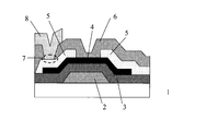
- FIG. 1 is a schematic cross-sectional view for explaining a thin film transistor including an oxide semiconductor.
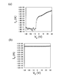
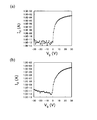
- 2A and 2B are diagrams showing TFT characteristics before and after the formation of the protective film when ZTO (conventional example) is used.
- FIG. 2A shows the TFT characteristics before the protective film is formed.
- FIG. 2B shows the TFT characteristics after forming the protective film.
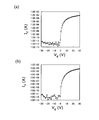
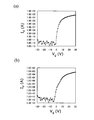
- 3A and 3B are diagrams showing TFT characteristics before and after the formation of the protective film when ZTO-Al is used, and
- FIG. 3A shows the TFT characteristics before the protective film is formed.
- (B) shows the TFT characteristics after protective film formation.
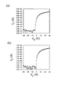
- 4A and 4B are diagrams showing TFT characteristics before and after the formation of the protective film when ZTO-Hf is used, and FIG.
- FIG. 4A shows the TFT characteristics before the protective film is formed.
- (B) shows the TFT characteristics after protective film formation.
- 5A and 5B are diagrams showing TFT characteristics before and after the formation of the protective film when ZTO-Ta is used.
- FIG. 5A shows TFT characteristics before the protective film is formed.
- (B) shows the TFT characteristics after protective film formation.
- 6A and 6B are diagrams showing TFT characteristics before and after the formation of the protective film when ZTO-Ti is used, and FIG. 6A shows the TFT characteristics before the protective film is formed.
- (B) shows the TFT characteristics after protective film formation.
- 7A and 7B are diagrams showing TFT characteristics before and after the formation of the protective film when ZTO-Nb is used, and FIG. 7A shows the TFT characteristics before the protective film is formed.
- FIG. 8A and 8B are diagrams showing the TFT characteristics before and after the formation of the protective film when ZTO-Mg is used, and FIG. 8A shows the TFT characteristics before the protective film is formed.
- FIG. 8A shows the TFT characteristics before the protective film is formed.
- FIG. 9A and 9B are diagrams showing TFT characteristics before and after the formation of the protective film when ZTO-Sc is used, and FIG. 9A shows the TFT characteristics before the protective film is formed.
- (B) shows the TFT characteristics after protective film formation.
- 10A and 10B are diagrams showing TFT characteristics before and after the formation of the protective film when ZTO-Y is used, and FIG. 10A shows the TFT characteristics before the protective film is formed.
- FIG. 11A and 11B are diagrams showing TFT characteristics before and after the formation of the protective film when ZTO-Ga is used, and FIG. 11A shows the TFT characteristics before the protective film is formed.
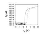
- FIG. 12 shows TFT characteristics before and after stress application when ZTO-Mg is used. A dotted line shows TFT characteristics before stress application, and a solid line shows TFT characteristics after stress application.
- FIG. 13 is a diagram showing TFT characteristics before and after stress application when ZTO-Nb is used. A dotted line shows TFT characteristics before stress application, and a solid line shows TFT characteristics after stress application.
- FIG. 14 is a diagram showing TFT characteristics before and after stress application when ZTO-Sc is used.
- a dotted line shows TFT characteristics before stress application, and a solid line shows TFT characteristics after stress application.
- FIG. 15 is a diagram showing TFT characteristics before and after stress application when ZTO-Ti is used.
- a dotted line shows TFT characteristics before stress application, and a solid line shows TFT characteristics after stress application.
- FIG. 16 is a diagram showing TFT characteristics before and after stress application when ZTO-Al is used.
- a dotted line shows TFT characteristics before stress application, and a solid line shows TFT characteristics after stress application.
- FIG. 17 is a diagram showing TFT characteristics before and after stress application when ZTO-Hf is used.
- FIG. 18 is a diagram showing TFT characteristics before and after stress application when ZTO (conventional example) is used.
- a dotted line shows TFT characteristics before stress application, and a solid line shows TFT characteristics after stress application.
- FIG. 19 is a diagram showing TFT characteristics before and after stress application when ZTO-Ta is used.
- a dotted line shows TFT characteristics before stress application, and a solid line shows TFT characteristics after stress application.
- FIG. 20 is a diagram showing TFT characteristics before and after stress application when ZTO-Ga is used.
- a dotted line shows TFT characteristics before stress application, and a solid line shows TFT characteristics after stress application.
- FIG. 21 is a diagram showing TFT characteristics before and after stress application when ZTO-Y is used.
- a dotted line shows TFT characteristics before stress application and a solid line shows TFT characteristics after stress application.
- a TFT including an oxide semiconductor containing an element belonging to the X group is more particularly a protective film than the case of using a conventional ZTO to which no X group element is added. It was found that the TFT characteristics after formation and after stress application were extremely excellent.
- the oxide for a semiconductor layer of the thin film transistor (TFT) according to the present invention is at least one selected from the group X consisting of Zn and Sn; and Al, Hf, Ta, Ti, Nb, Mg, Ga, and rare earth elements.
- This element is characterized in that it contains the element (which may be represented by an X group element).
- the oxide of the present invention may be represented by ZTO-X or ZTO + X.
- metals (Zn and Sn), which are base material components constituting the oxide of the present invention will be described.
- the ratio between the metals (Zn, Sn) is not particularly limited as long as the oxide (ZTO) containing these metals has an amorphous phase and exhibits semiconductor characteristics.
- ZTO oxide
- the crystal phase is formed, there is a possibility that problems such as large variations in transistor characteristics may occur.
- the ratio is 0.8 or less, whereby desired TFT characteristics can be obtained.
- the ratio is preferably 0.2 or more, and more preferably 0.3 or more.
- the oxide of the present invention contains an X group element in ZTO.
- group X element selected from the group consisting of Al, Hf, Ta, Ti, Nb, Mg, Ga, and rare earth elements (group X) into ZTO, this is a region where the amount of Zn is large.
- group X rare earth elements
- good TFT characteristics can be stably obtained without making ZTO-X a conductor.
- the “rare earth element” is an element group in which Sc (scandium) and Y (yttrium) are added to a lanthanoid element (a total of 15 elements from La of atomic number 57 to Lu of atomic number 71 in the periodic table). And one or more rare earth elements can be used.
- the X group element has an effect of suppressing the generation of oxygen vacancies that cause surplus electrons in the oxide semiconductor. It is considered that the addition of the group X element reduces oxygen vacancies and prevents the entire ZTO-X or the surface from becoming a conductor because the oxide has a stable structure.
- the preferred ratio [X / (Zn + Sn + X)] of the group X elements contained in all the metals (Zn, Sn, group X elements) constituting the oxide (ZTO-X) of the present invention is the carrier density, the stability of the semiconductor, etc. However, it is slightly different depending on the type of the X group element.
- Ga is included as the X group element, the preferable upper limit of the ratio can be increased as compared with the case where Ga is not included.
- Ga content (atomic%) contained in the oxide (ZTO-X) is [Ga], [Ga] / ([Zn] + [Sn] + [Ga]) is preferable.
- the ratio is 0.01 or more and 0.5 or less.
- [X1] when it contains 2 or more types of X group elements other than Ga, it is these total amount, and when it contains X group elements other than Ga independently, it is a single amount. If the addition ratio of [Ga] or [X1] is too small, the effect of suppressing the occurrence of oxygen vacancies may not be sufficiently obtained. On the other hand, if the addition ratio of [Ga] or [X1] is too large, the on-current may be likely to decrease because the carrier density or mobility in the semiconductor decreases.
- a preferable range of the mobility is 3 cm 2 / Vs or more in the saturation region, more preferably 5 cm 2 / Vs or more, and further preferably 7.5 cm 2 / Vs or more.
- the X group element has an effect of suppressing the generation of oxygen vacancies that cause surplus electrons in the oxide semiconductor. It is considered that oxygen vacancies are reduced by the addition of the group X element, and the stress resistance against stresses such as voltage and light is improved because the oxide has a stable structure.
- the oxide is preferably formed by a sputtering method using a sputtering target (hereinafter also referred to as “target”).
- a sputtering target hereinafter also referred to as “target”.
- an oxide can be formed by a chemical film formation method such as a coating method, a thin film excellent in in-plane uniformity of components and film thickness can be easily formed by a sputtering method.
- a thin film having a desired composition ratio can be formed by appropriately synthesizing each ratio of ZnO, SnO 2 , and group X element-O including the above-described elements.
- an oxide target containing Zn and Sn; and at least one element selected from the group consisting of Al, Hf, Ta, Ti, Nb, Mg, Ga, and rare earth elements (group X) is used as a target.
- group X rare earth elements
- a film may be formed by using a co-sputtering method (Co-Sputter method) in which two targets having different compositions are discharged at the same time, whereby oxide semiconductor films having different X element contents in the same substrate surface.
- Co-Sputter method a co-sputtering method
- three targets, a ZnO target, a ZTO (or SnO 2 ) target, and a target made of an oxide of an X group element are prepared, and a desired ZTO-X is prepared by co-sputtering.
- the oxide can be formed.
- the target can be manufactured by, for example, a powder sintering method.
- Sputtering using the target is preferably performed by setting the substrate temperature to room temperature and appropriately controlling the amount of oxygen added.
- a preferable density of the oxide semiconductor layer is 5.8 g / cm 3 or more (described later). It is preferable to appropriately control the gas pressure during sputtering film formation, the input power to the sputtering target, the substrate temperature, and the like. For example, if the gas pressure at the time of film formation is lowered, it is considered that a dense (high density) film can be formed because the sputtering atoms do not scatter, so the total gas pressure at the time of film formation is such that the discharge of the sputtering is stable.
- the preferable film thickness of the oxide formed as described above is 30 nm to 200 nm, and more preferably 30 nm to 150 nm.
- the present invention includes a TFT including the oxide as a semiconductor layer of the TFT.
- a TFT only needs to have at least a gate electrode, a gate insulating film, a semiconductor layer of the above oxide, a source electrode, a drain electrode, and a protective film (insulating film) on a substrate, and its configuration is usually used. If there is no particular limitation.
- the density of the oxide semiconductor layer is preferably 5.8 g / cm 3 or more.
- the density of the oxide semiconductor layer is increased, defects in the film are reduced, the film quality is improved, and the interatomic distance is reduced, so that the field effect mobility of the TFT element is greatly increased, and the electrical conductivity is also increased. Stability to stress against light irradiation is improved.
- the higher the density of the oxide semiconductor layer the better, more preferably 5.9 g / cm 3 or more, and still more preferably 6.0 g / cm 3 or more. Note that the density of the oxide semiconductor layer is measured by a method described in Examples described later.
- FIG. 1 illustrates a bottom-gate TFT, but the present invention is not limited to this.
- a top-gate TFT including a gate insulating film and a gate electrode in this order on an oxide semiconductor layer may be used.
- a gate electrode 2 and a gate insulating film 3 are formed on a substrate 1, and an oxide semiconductor layer 4 is formed thereon.
- a source / drain electrode 5 is formed on the oxide semiconductor layer 4, a protective film (insulating film) 6 is formed thereon, and the transparent conductive film 8 is electrically connected to the drain electrode 5 through the contact hole 7.
- the method for forming the gate electrode 2 and the gate insulating film 3 on the substrate 1 is not particularly limited, and a commonly used method can be employed. Further, the types of the substrate 1, the gate electrode 2, and the gate insulating film 3 are not particularly limited, and those that are widely used can be used. For example, glass or the like can be preferably used as the substrate 1. Further, as the gate electrode 2, an Al or Cu metal having a low electrical resistivity or an alloy thereof can be preferably used.
- the gate insulating film 3 is typically exemplified by a silicon oxide film, a silicon nitride film, a silicon oxynitride film, and the like. In addition, oxides such as Al 2 O 3 and Y 2 O 3 and those obtained by stacking these can also be used.
- the oxide semiconductor layer 4 is formed.
- the oxide semiconductor layer 4 is preferably formed by a DC sputtering method or an RF sputtering method using a sputtering target having the same composition as the thin film.
- the film may be formed by co-sputtering.
- the oxide semiconductor layer 4 is subjected to wet etching and then patterned. Immediately after the patterning, it is preferable to perform heat treatment (pre-annealing) for improving the film quality of the oxide semiconductor layer 4 so that the on-state current and field-effect mobility of the transistor characteristics are increased and the transistor performance is improved. Become.
- the source / drain electrodes 5 are formed.
- the type of the source / drain electrode 5 is not particularly limited, and a commonly used one can be used.
- a metal or an alloy such as Al or Cu may be used similarly to the gate electrode 2, or pure Ti may be used as in the examples described later.
- a metal thin film can be formed by a magnetron sputtering method and then formed by a lift-off method.
- a protective film (insulating film) 6 is formed over the oxide semiconductor layer 4 by a CVD (Chemical Vapor Deposition) method.
- the surface of the oxide semiconductor layer 4 may be easily made conductive by plasma damage caused by CVD (probably because oxygen vacancies generated on the surface of the oxide semiconductor become electron donors).
- N 2 O plasma irradiation was performed before the formation of the protective film. The conditions described in the following document are adopted as the N 2 O plasma irradiation conditions, and the contents thereof are incorporated herein by reference. J. et al. Park et al., Appl. Phys. Lett. 1993, 053505 (2008).
- the transparent conductive film 8 is electrically connected to the drain electrode 5 through the contact hole 7.
- the types of the transparent conductive film and the drain electrode are not particularly limited, and commonly used ones can be used.
- As the transparent conductive film ITO, IZO or the like can be preferably used.
- As a drain electrode what was illustrated by the source / drain electrode mentioned above, for example can be used.
- Example 1 Based on the method described above, the thin film transistor (TFT) shown in FIG. 1 was fabricated, and the TFT characteristics before and after the formation of the protective film were evaluated.
- TFT thin film transistor
- a Ti thin film of 100 nm and a gate insulating film SiO 2 were sequentially formed as a gate electrode on a glass substrate (Corning Eagle 2000, diameter 100 mm ⁇ thickness 0.7 mm).
- the gate electrode was formed using a pure Ti sputtering target by DC sputtering at a film forming temperature: room temperature, a film forming power: 300 W, a carrier gas: Ar, and a gas pressure: 2 mTorr.
- the gate insulating film was formed using a plasma CVD method with a carrier gas: a mixed gas of SiH 4 and N 2 O, a deposition power of 100 W, and a deposition temperature of 300 ° C.
- oxide thin films having various compositions described in Table 1 were formed by a sputtering method using a sputtering target (described later).
- a sputtering target described later.
- ZTO-X containing Z group element in ZTO example of the present invention
- ZTO containing no X group element conventional example
- the apparatus used for sputtering is “CS-200” manufactured by ULVAC, Inc., and the sputtering conditions are as follows.
- Substrate temperature room temperature
- Gas pressure 5 mTorr
- Oxygen partial pressure: O 2 / (Ar + O 2 ) 2%
- Use target size ⁇ 4 inch x 5mm
- the film is formed using a Co-Sputter method in which an oxide target (ZTO) having a Zn: Sn ratio (atomic% ratio) of 6: 4 and a ZnO target are simultaneously discharged. did.
- ZTO oxide target
- the target used for forming the ZTO film that is, an oxide target having a Zn: Sn ratio (atomic% ratio) of 6: 4].
- ZTO and ZnO target] and an oxide target of the X group element were formed using a Co-Sputter method in which discharge was performed simultaneously.
- Each content of the metal element in the oxide thin film thus obtained was analyzed by an XPS (X-ray Photoelectron Spectroscopy) method. Specifically, after sputtering a range from the outermost surface to a depth of about 1 nm with Ar ions, analysis was performed under the following conditions.
- X-ray source Al K ⁇
- X-ray output 350W
- Photoelectron extraction angle 20 °
- Pre-annealing was performed to improve the film quality. Pre-annealing was performed at 350 ° C. for 1 hour under atmospheric pressure.
- pure Ti was used to form source / drain electrodes by a lift-off method. Specifically, after patterning using a photoresist, a Ti thin film was formed by DC sputtering (film thickness was 100 nm). The method for forming the Ti thin film for the source / drain electrodes is the same as that for the gate electrode described above. Next, an unnecessary photoresist was removed by applying an ultrasonic cleaner in acetone, and the TFT channel length was 10 ⁇ m and the channel width was 200 ⁇ m.
- a protective film for protecting the oxide semiconductor layer was formed.
- a laminated film (total film thickness 400 nm) of SiO 2 (film thickness 200 nm) and SiN (film thickness 200 nm) was used.
- the formation of the SiO 2 and SiN was performed using “PD-220NL” manufactured by Samco and using the plasma CVD method.
- SiO 2 and SiN films were sequentially formed.
- a mixed gas of N 2 O and SiH 4 was used for forming the SiO 2 film, and a mixed gas of SiH 4 , N 2 , and NH 3 was used for forming the SiN film.
- the film formation power was 100 W and the film formation temperature was 150 ° C.
- ITO film film thickness: 80 nm
- a carrier gas a mixed gas of argon and oxygen gas
- film formation power 200 W
- gas pressure 5 mTorr
- transistor characteristics drain current-gate voltage characteristics, Id-Vg characteristics
- threshold voltage threshold voltage
- Threshold voltage The threshold voltage is roughly a value of a gate voltage when the transistor shifts from an off state (a state where the drain current is low) to an on state (a state where the drain current is high).
- the voltage when the drain current is around 1 nA between the on-current and the off-current is defined as the threshold voltage, and the threshold voltage for each TFT is measured.
- S value is the minimum value of the gate voltage required to increase the drain current by one digit.
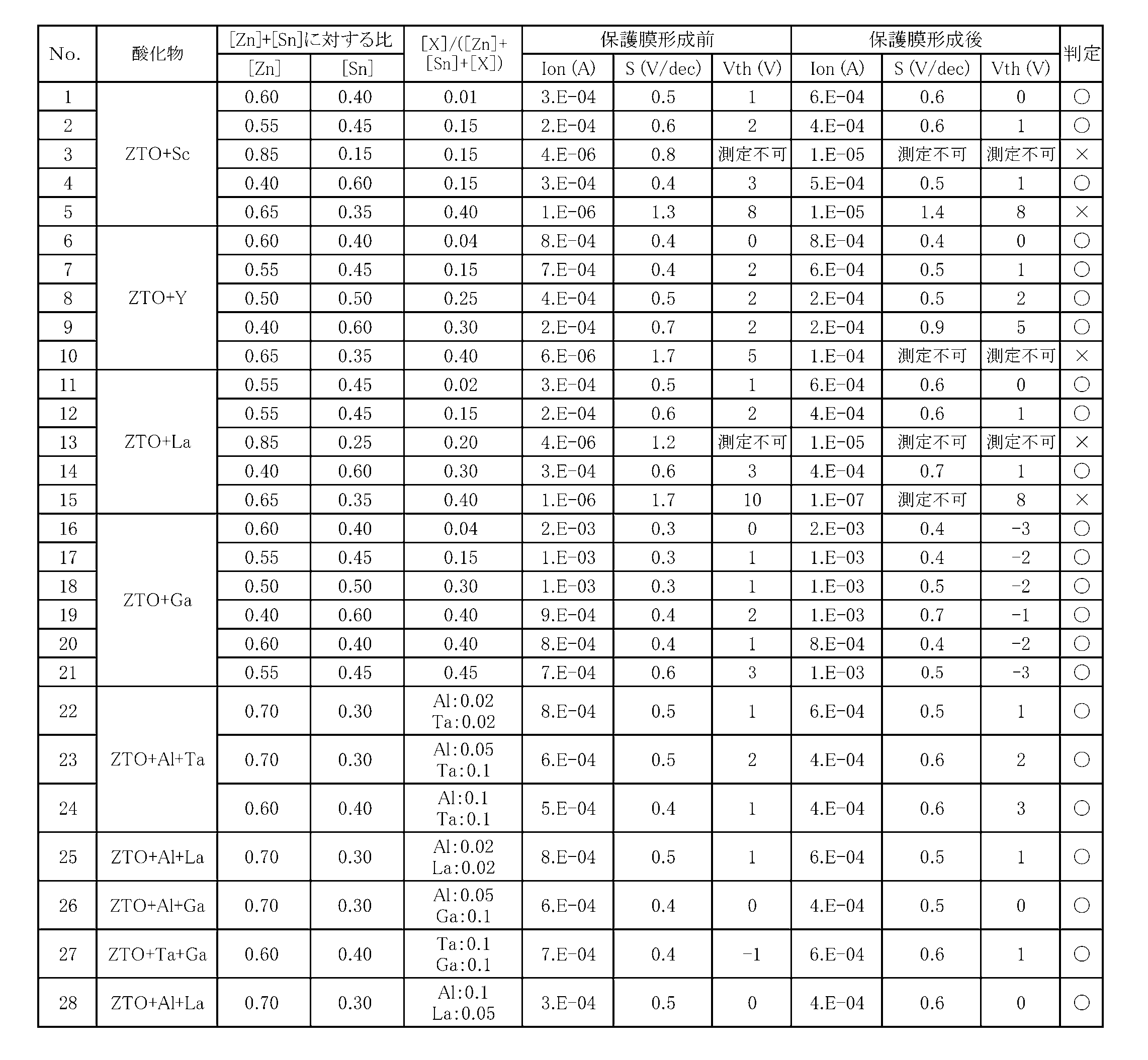
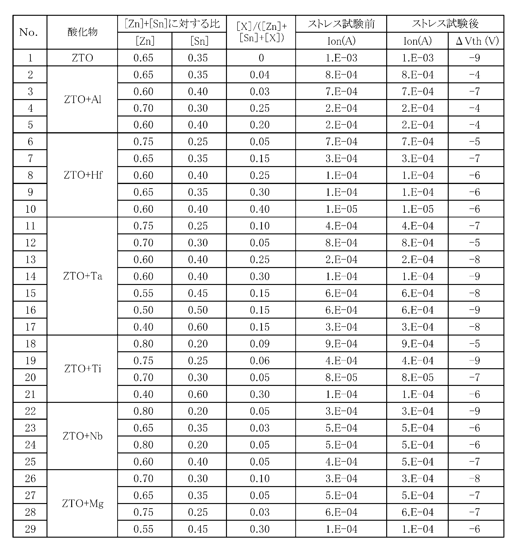
- Table 1 shows values of on-current (Ion), threshold voltage, and S value before and after the formation of the protective film.
- Ion on-current
- threshold voltage threshold voltage
- S S value before and after the formation of the protective film.
- each characteristic was good when Ion ⁇ 1 ⁇ 10 ⁇ 5 A, ⁇ 10 V ⁇ Vth ⁇ 10 V, and S ⁇ 1.0 V / dec.
- judgment In the rightmost column of Table 1 and Table 2, there is a column of “judgment”, where all the characteristics before and after the formation of the protective film are marked with “good”, and any one of the characteristics is not good with “x” I attached.
- E-0X means E ⁇ 10 ⁇ 0X .
- E-04 means 2 ⁇ 10 ⁇ 4 .
- ZTO + Al (No. 3 in Table 1) is an example containing Al as an X group element.
- the metal in the oxide is composed of Zn, Sn, and Al
- the atomic ratio of [Al] to [Zn] + [Sn] + [Al] is 0.04
- [Zn] It means that the atomic ratio of [Zn] to + [Sn] is 0.70.
- the metal in the oxide is composed of Zn, Sn, Al, and La.
- the atomic ratio of [Al] to [Zn] + [Sn] + [Al] + [La] is 0.02, and [Zn] + [Sn] + [Al] + [La] It means that the atomic ratio of La] is 0.02, and the atomic ratio of [Zn] to [Zn] + [Sn] is 0.70.
- FIGS. 3A and 3B are examples in which Al is included as an X group element, and the metal in the oxide is composed of Zn, Sn, and Al.
- FIGS. 5A and 5B are examples in which Ta is included as an X group element, and the metal in the oxide is composed of Zn, Sn, and Ta.
- [Zn] + [Sn] + [Ta] is an example in which the atomic ratio of [Ta] is 0.04, and the atomic ratio of [Zn] to [Zn] + [Sn] is 0.6.
- FIGS. 6A and 6B are examples in which Ti is included as an X group element, and the metal in the oxide is composed of Zn, Sn, and Ti.
- [Zn] + [Sn] + [Ti the atomic ratio of [Ti] to [Zn] is 0.04, and the atomic ratio of [Zn] to [Zn] + [Sn] is 0.65.
- FIGS. 7A and 7B are examples in which Nb is included as an X group element, and the metal in the oxide is composed of Zn, Sn, and Nb.
- [Zn] + [Sn] + [Nb ] The atomic ratio of [Nb] to 0.04 and [Zn] to [Zn] + [Sn] is 0.6.
- FIGS. 8A and 8B are examples in which Mg is included as an X group element, and the metal in the oxide is composed of Zn, Sn, and Mg.
- [Zn] + [Sn] + [Mg ] The atomic ratio of [Mg] is 0.04, and the atomic ratio of [Zn] to [Zn] + [Sn] is 0.65.
- FIGS. 9A and 9B are examples in which Sc is included as the X group element and the metal in the oxide is composed of Zn, Sn, and Sc.
- [Zn] + [Sn] + [Sc ] The atomic ratio of [Sc] to 0.04 and [Zn] to [Zn] + [Sn] is 0.6.
- FIGS. 10A and 10B are examples in which Y is included as the X group element, and the metal in the oxide is composed of Zn, Sn, and Y.
- [Zn] + [Sn] + [Y the atomic ratio of [Y] to [Zn] is 0.04, and the atomic ratio of [Zn] to [Zn] + [Sn] is 0.65.
- 11A and 11B are examples in which Ga is included as an X group element, and the metal in the oxide is composed of Zn, Sn, and Ga.
- [Zn] + [Sn] + [Ga In this example, the atomic ratio of [Ga] to [] is 0.04, and the atomic ratio of [Zn] to [Zn] + [Sn] is 0.6.
- the on-current Ion, the S value, and the threshold voltage Vth were all good, but after the protective film was formed, the threshold value could not be measured, and the S value increased or It was not possible to measure.
- the drain current Id started to increase from the gate voltage Vg of around ⁇ 10 V before the protective film was formed, and a switching operation was observed [see FIG. 2 (a)]. After the film formation, no switching operation was observed at all as shown in FIG.
- the ratio of the Zn amount to the total amount of Zn and Sn tended to decrease the TFT characteristics (increase in Ion, decrease in S value and Vth) as the ratio decreased. According to the present invention, it has been confirmed that even when the ratio is increased to about 0.5 to 0.8 (that is, even in a region with a large amount of ZnO), good TFT characteristics can be obtained.
- the oxide does not become a conductor before and after the formation of the protective film, and stable TFT characteristics can be obtained even by the formation of the protective film. It was confirmed that it was obtained. Moreover, since the wet etching process was also performed well, it is presumed that the oxide added with the X group element has an amorphous structure.
- Example 2 In this example, various TFT thin films described in Table 1 and Table 2 were used, and for each TFT fabricated in the same manner as Example 1, (4) stress resistance before and after stress application was as follows. evaluated.
- Id-Vg characteristics drain current-gate voltage characteristics
- the drain current Id started to increase from around ⁇ 3 V of the gate voltage Vg, and a switching operation was observed.
- Ion was 1.0 ⁇ 10 ⁇ 3 A after stress application (see Table 3), and these values hardly changed before and after stress application, but as shown in FIG. The value voltage was greatly changed, and the threshold voltage shift amount from 0 hour (no stress) to 1 hour (stress application) was ⁇ 9 V (see Table 3).
- Example 1 From the results of Example 1 and Example 2 above, it was confirmed that if the oxide of the present invention was used, good TFT characteristics could be obtained even after formation of the protective film and after application of stress.
- the density of the oxide film was measured using XRR (X-ray reflectivity method). Detailed measurement conditions are as follows.
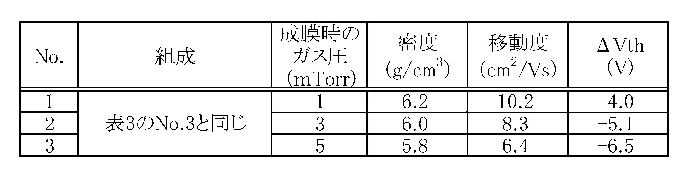
- regulated by this invention all obtained the high density of 5.8 g / cm ⁇ 3 > or more.
- the film density when the gas pressure was 5 mTorr (No. 3) was 5.8 g / cm 3
- the film density when the gas pressure was 3 mTorr (No. 2) was 6.0 g. / cm 3
- the film density at a gas pressure 1 mTorr (No.1) is 6.2 g / cm 3 as the gas pressure becomes lower, a higher density is obtained.
- the film density increased, the field effect mobility improved, and the absolute value of the threshold voltage shift amount ⁇ Vth by the stress test also decreased.
- the density of the oxide film changes depending on the gas pressure during sputtering film formation, and when the gas pressure is lowered, the film density increases, and the field effect mobility greatly increases with this, and the stress test It was found that the absolute value of the threshold voltage shift amount ⁇ Vth in (light irradiation + negative bias stress) also decreases. This is because by reducing the gas pressure during sputtering film formation, turbulence of the sputtered atoms (molecules) can be suppressed, defects in the film are reduced, mobility and electrical conductivity are improved, and TFT stability is improved. This is presumed to be due to improved performance.
- a ZTO-based oxide for a semiconductor layer excellent in switching characteristics and stress resistance of a thin film transistor was obtained. If the oxide for semiconductor layers of the present invention is used, the region where the ZnO concentration in the oxide semiconductor is high (specifically, the ratio (atomic ratio) of Zn in the Zn and Sn constituting the oxide semiconductor is approximately) A thin film transistor capable of stably obtaining good characteristics even after formation of a protective film and after application of stress can be provided. As a result, when the thin film transistor is used, a highly reliable display device can be obtained.
Landscapes
- Thin Film Transistor (AREA)
- Physical Vapour Deposition (AREA)
- Physical Deposition Of Substances That Are Components Of Semiconductor Devices (AREA)
Abstract
Description
(1)薄膜トランジスタの半導体層に用いられる酸化物であって、
前記酸化物は、ZnおよびSnを含み、Al、Hf、Ta、Ti、Nb、Mg、Ga、および希土類元素よりなるX群から選択される少なくとも一種の元素を更に含む薄膜トランジスタの半導体層用酸化物。
(2)半導体層用酸化物に含まれるZnおよびSnの含有量(原子%)をそれぞれ、[Zn]および[Sn]としたとき、[Zn]/([Zn]+[Sn])の比が0.8以下である(1)に記載の酸化物。
(3)前記X群の元素としてGaを含むとき、半導体層用酸化物に含まれるGaの含有量(原子%)を[Ga]とすると、[Ga]/([Zn]+[Sn]+[Ga])の比が0.01以上0.5以下であり、前記X群の元素としてGa以外の元素(X1)を含むとき、半導体層用酸化物に含まれるX1の合計量(原子%)を[X1]とすると、[X1]/([Zn]+[Sn]+[X1])の比が0.01以上0.3以下である(1)または(2)に記載の酸化物。
(4)(1)~(3)のいずれかに記載の酸化物を薄膜トランジスタの半導体層として備えた薄膜トランジスタ。
(5)前記半導体層の密度は5.8g/cm3以上である(4)に記載の薄膜トランジスタ。
(6)(1)~(3)のいずれかに記載の酸化物を形成するためのスパッタリングターゲットであって、ZnおよびSnを含み、Al、Hf、Ta、Ti、Nb、Mg、Ga、および希土類元素よりなるX群から選択される少なくとも一種の元素を更に含むスパッタリングターゲット。
(7)スパッタリングターゲットに含まれるZnおよびSnの含有量(原子%)をそれぞれ、[Zn]および[Sn]としたとき、[Zn]/([Zn]+[Sn])の比が0.8以下である(6)に記載のスパッタリングターゲット。
(8)前記X群の元素としてGaを含むとき、スパッタリングターゲットに含まれるGaの含有量(原子%)を[Ga]とすると、[Ga]/([Zn]+[Sn]+[Ga])の比が0.01以上0.5以下であり、前記X群の元素としてGa以外の元素(X1)を含むとき、スパッタリングターゲットに含まれるX1の合計量(原子%)を[X1]とすると、[X1]/([Zn]+[Sn]+[X1])の比が0.01以上0.3以下である(6)または(7)に記載のスパッタリングターゲット。
J. Parkら、Appl. Phys. Lett., 1993,053505(2008)。
前述した方法に基づき、図1に示す薄膜トランジスタ(TFT)を作製し、保護膜形成前後のTFT特性を評価した。
基板温度:室温
ガス圧:5mTorr
酸素分圧:O2/(Ar+O2)=2%
膜厚:50~150nm
使用ターゲットサイズ:φ4インチ×5mm
X線源:Al Kα
X線出力:350W
光電子取り出し角:20°
トランジスタ特性の測定はNational Instruments社製「4156C」の半導体パラメータアナライザーを使用した。詳細な測定条件は以下のとおりである。本実施例では、Vg=30Vのときのオン電流(Ion)を算出した。
ソース電圧 :0V
ドレイン電圧:10V
ゲート電圧 :-30~30V(測定間隔:1V)
しきい値電圧とは、おおまかにいえば、トランジスタがオフ状態(ドレイン電流の低い状態)からオン状態(ドレイン電流の高い状態)に移行する際のゲート電圧の値である。本実施例では、ドレイン電流が、オン電流とオフ電流の間の1nA付近であるときの電圧をしきい値電圧と定義し、各TFT毎のしきい値電圧を測定した。
S値は、ドレイン電流を一桁増加させるのに必要なゲート電圧の最小値とした。

各図において、(a)は保護膜形成前の結果を、(b)は保護膜形成後の結果をそれぞれ示している。
図3(a)及び(b)は、X群元素としてAlを含み、酸化物中の金属がZnとSnとAlとから構成されている例であり、[Zn]+[Sn]+[Al]に対する[Al]の原子比が0.04であり、且つ、[Zn]+[Sn]に対する[Zn]の原子比が0.7である例である。
図4(a)及び(b)は、X群元素としてHfを含み、酸化物中の金属がZnとSnとHfとから構成されている例であり、[Zn]+[Sn]+[Hf]に対する[Hf]の原子比が0.04であり、且つ、[Zn]+[Sn]に対する[Zn]の原子比が0.65である例である。
図5(a)及び(b)は、X群元素としてTaを含み、酸化物中の金属がZnとSnとTaとから構成されている例であり、[Zn]+[Sn]+[Ta]に対する[Ta]の原子比が0.04であり、且つ、[Zn]+[Sn]に対する[Zn]の原子比が0.6である例である。
図6(a)及び(b)は、X群元素としてTiを含み、酸化物中の金属がZnとSnとTiとから構成されている例であり、[Zn]+[Sn]+[Ti]に対する[Ti]の原子比が0.04であり、且つ、[Zn]+[Sn]に対する[Zn]の原子比が0.65である例である。
図7(a)及び(b)は、X群元素としてNbを含み、酸化物中の金属がZnとSnとNbとから構成されている例であり、[Zn]+[Sn]+[Nb]に対する[Nb]の原子比が0.04であり、且つ、[Zn]+[Sn]に対する[Zn]の原子比が0.6である例である。
図8(a)及び(b)は、X群元素としてMgを含み、酸化物中の金属がZnとSnとMgとから構成されている例であり、[Zn]+[Sn]+[Mg]に対する[Mg]の原子比が0.04であり、且つ、[Zn]+[Sn]に対する[Zn]の原子比が0.65である例である。
図9(a)及び(b)は、X群元素としてScを含み、酸化物中の金属がZnとSnとScとから構成されている例であり、[Zn]+[Sn]+[Sc]に対する[Sc]の原子比が0.04であり、且つ、[Zn]+[Sn]に対する[Zn]の原子比が0.6である例である。
図10(a)及び(b)は、X群元素としてYを含み、酸化物中の金属がZnとSnとYとから構成されている例であり、[Zn]+[Sn]+[Y]に対する[Y]の原子比が0.04であり、且つ、[Zn]+[Sn]に対する[Zn]の原子比が0.65である例である。
図11(a)及び(b)は、X群元素としてGaを含み、酸化物中の金属がZnとSnとGaとから構成されている例であり、[Zn]+[Sn]+[Ga]に対する[Ga]の原子比が0.04であり、且つ、[Zn]+[Sn]に対する[Zn]の原子比が0.6である例である。
本実施例では、表1および表2に記載の種々の酸化物薄膜を用い、実施例1と同様にして作製した各TFTについて、以下のようにして、(4)ストレス印加前後におけるストレス耐性を評価した。
本実施例では、実際のパネル駆動時の環境(ストレス)を模擬して、ゲート電極に負バイアスをかけながら光を照射するストレス印加試験を行った。ストレス印加条件は以下のとおりである。光の波長としては、酸化物半導体のバンドギャップに近く、トランジスタ特性が変動し易い400nm程度を選択した。
ゲート電圧:-20V
ドレイン電圧:10V
基板温度:60℃
光ストレス
波長:400nm
照度(TFTに照射される光の強度):80nW/cm2
光源:OPTOSUPPLY社製LED(NDフィルターによって光量を調整)
ストレス印加時間:1時間


本実施例では、表3のNo.3に対応する組成の酸化物(ZnSnO+3at%Al、[Zn]:[Sn]=6:4、Zn比=[Zn]/[Zn]+[Sn]=0.6、Al比=[Al]/[Zn]+[Sn]+[Al]=0.03)を用い、スパッタリング成膜時のガス圧を1mTorr、3mTorr、または5mTorrに制御して得られた酸化物膜(膜厚100nm)の密度を測定すると共に、前述した実施例2と同様にして作成したTFTについて、移動度およびストレス試験(光照射+負バイアスを印加)後のしきい値電圧の変化量(ΔVth)を調べた。膜密度の測定法方は以下のとおりである。
酸化物膜の密度は、XRR(X線反射率法)を用いて測定した。詳細な測定条件は以下のとおりである。
・ターゲット:Cu(線源:Kα線)
・ターゲット出力:45kV-200mA
・測定試料の作製
ガラス基板上に各組成の酸化物を下記スパッタリング条件で成膜した(膜厚100nm)後、前述した実施例1のTFT製造過程におけるプレアニール処理を模擬して、当該プレアニール処理と同じ熱処理を施したしたものを使用
スパッタガス圧:1mTorr、3mTorrまたは5mTorr
酸素分圧:O2/(Ar+O2)=2%
成膜パワー密度:DC2.55W/cm2
熱処理:大気雰囲気にて350℃で1時間
本出願は、2010年4月20日出願の日本特許出願(特願2010-097350)、2010年7月8日出願の日本特許出願(特願2010-156232)、2011年1月18日出願の日本特許出願(特願2011-008324)に基づくものであり、その内容はここに参照として取り込まれる。
2 ゲート電極
3 ゲート絶縁膜
4 酸化物半導体層
5 ソース・ドレイン電極
6 保護膜(絶縁膜)
7 コンタクトホール
8 透明導電膜
Claims (10)
- 薄膜トランジスタの半導体層に用いられる酸化物であって、
前記酸化物は、ZnおよびSnを含み、Al、Hf、Ta、Ti、Nb、Mg、Ga、および希土類元素よりなるX群から選択される少なくとも一種の元素を更に含む薄膜トランジスタの半導体層用酸化物。 - 半導体層用酸化物に含まれるZnおよびSnの含有量(原子%)をそれぞれ、[Zn]および[Sn]としたとき、[Zn]/([Zn]+[Sn])の比が0.8以下である請求項1に記載の酸化物。
- 前記X群の元素としてGaを含むとき、半導体層用酸化物に含まれるGaの含有量(原子%)を[Ga]とすると、[Ga]/([Zn]+[Sn]+[Ga])の比が0.01以上0.5以下であり、前記X群の元素としてGa以外の元素(X1)を含むとき、半導体層用酸化物に含まれるX1の合計量(原子%)を[X1]とすると、[X1]/([Zn]+[Sn]+[X1])の比が0.01以上0.3以下である請求項1に記載の酸化物。
- 前記X群の元素としてGaを含むとき、半導体層用酸化物に含まれるGaの含有量(原子%)を[Ga]とすると、[Ga]/([Zn]+[Sn]+[Ga])の比が0.01以上0.5以下であり、前記X群の元素としてGa以外の元素(X1)を含むとき、半導体層用酸化物に含まれるX1の合計量(原子%)を[X1]とすると、[X1]/([Zn]+[Sn]+[X1])の比が0.01以上0.3以下である請求項2に記載の酸化物
- 請求項1~4のいずれかに記載の酸化物を薄膜トランジスタの半導体層として備えた薄膜トランジスタ。
- 前記半導体層の密度は5.8g/cm3以上である請求項5に記載の薄膜トランジスタ。
- 請求項1~4のいずれかに記載の酸化物を形成するためのスパッタリングターゲットであって、ZnおよびSnを含み、Al、Hf、Ta、Ti、Nb、Mg、Ga、および希土類元素よりなるX群から選択される少なくとも一種の元素を更に含むスパッタリングターゲット。
- スパッタリングターゲットに含まれるZnおよびSnの含有量(原子%)をそれぞれ、[Zn]および[Sn]としたとき、[Zn]/([Zn]+[Sn])の比が0.8以下である請求項7に記載のスパッタリングターゲット。
- 前記X群の元素としてGaを含むとき、スパッタリングターゲットに含まれるGaの含有量(原子%)を[Ga]とすると、[Ga]/([Zn]+[Sn]+[Ga])の比が0.01以上0.5以下であり、前記X群の元素としてGa以外の元素(X1)を含むとき、スパッタリングターゲットに含まれるX1の合計量(原子%)を[X1]とすると、[X1]/([Zn]+[Sn]+[X1])の比が0.01以上0.3以下である請求項7に記載のスパッタリングターゲット。
- 前記X群の元素としてGaを含むとき、スパッタリングターゲットに含まれるGaの含有量(原子%)を[Ga]とすると、[Ga]/([Zn]+[Sn]+[Ga])の比が0.01以上0.5以下であり、前記X群の元素としてGa以外の元素(X1)を含むとき、スパッタリングターゲットに含まれるX1の合計量(原子%)を[X1]とすると、[X1]/([Zn]+[Sn]+[X1])の比が0.01以上0.3以下である請求項8に記載のスパッタリングターゲット。
Priority Applications (3)
| Application Number | Priority Date | Filing Date | Title |
|---|---|---|---|
| KR1020127029973A KR101407402B1 (ko) | 2010-04-20 | 2011-04-18 | 박막 트랜지스터의 반도체층용 산화물 및 스퍼터링 타깃, 및 박막 트랜지스터 |
| CN201180019734.9A CN102859701B (zh) | 2010-04-20 | 2011-04-18 | 薄膜晶体管的半导体层用氧化物和溅射靶以及薄膜晶体管 |
| US13/642,314 US8907334B2 (en) | 2010-04-20 | 2011-04-18 | Oxide for semiconductor layer of thin-film transistor, sputtering target, and thin-film transistor |
Applications Claiming Priority (6)
| Application Number | Priority Date | Filing Date | Title |
|---|---|---|---|
| JP2010097350 | 2010-04-20 | ||
| JP2010-097350 | 2010-04-20 | ||
| JP2010-156232 | 2010-07-08 | ||
| JP2010156232 | 2010-07-08 | ||
| JP2011008324A JP2012033854A (ja) | 2010-04-20 | 2011-01-18 | 薄膜トランジスタの半導体層用酸化物およびスパッタリングターゲット、並びに薄膜トランジスタ |
| JP2011-008324 | 2011-01-18 |
Publications (1)
| Publication Number | Publication Date |
|---|---|
| WO2011132644A1 true WO2011132644A1 (ja) | 2011-10-27 |
Family
ID=44834163
Family Applications (1)
| Application Number | Title | Priority Date | Filing Date |
|---|---|---|---|
| PCT/JP2011/059554 Ceased WO2011132644A1 (ja) | 2010-04-20 | 2011-04-18 | 薄膜トランジスタの半導体層用酸化物およびスパッタリングターゲット、並びに薄膜トランジスタ |
Country Status (6)
| Country | Link |
|---|---|
| US (1) | US8907334B2 (ja) |
| JP (1) | JP2012033854A (ja) |
| KR (1) | KR101407402B1 (ja) |
| CN (1) | CN102859701B (ja) |
| TW (1) | TWI442576B (ja) |
| WO (1) | WO2011132644A1 (ja) |
Cited By (3)
| Publication number | Priority date | Publication date | Assignee | Title |
|---|---|---|---|---|
| CN103367455A (zh) * | 2012-04-02 | 2013-10-23 | 三星显示有限公司 | 半导体器件和薄膜晶体管 |
| CN103579360A (zh) * | 2012-08-07 | 2014-02-12 | 日立金属株式会社 | 氧化物半导体靶和氧化物半导体材料及半导体装置 |
| US9553201B2 (en) | 2012-04-02 | 2017-01-24 | Samsung Display Co., Ltd. | Thin film transistor, thin film transistor array panel, and manufacturing method of thin film transistor |
Families Citing this family (24)
| Publication number | Priority date | Publication date | Assignee | Title |
|---|---|---|---|---|
| JP5718072B2 (ja) | 2010-07-30 | 2015-05-13 | 三星ディスプレイ株式會社Samsung Display Co.,Ltd. | 薄膜トランジスタの半導体層用酸化物およびスパッタリングターゲット、並びに薄膜トランジスタ |
| JP5723262B2 (ja) | 2010-12-02 | 2015-05-27 | 株式会社神戸製鋼所 | 薄膜トランジスタおよびスパッタリングターゲット |
| JP5881681B2 (ja) * | 2011-04-12 | 2016-03-09 | 三井金属鉱業株式会社 | 酸化物型半導体材料及びスパッタリングターゲット |
| JP2012235104A (ja) | 2011-04-22 | 2012-11-29 | Kobe Steel Ltd | 薄膜トランジスタ構造、ならびにその構造を備えた薄膜トランジスタおよび表示装置 |
| KR101891650B1 (ko) * | 2011-09-22 | 2018-08-27 | 삼성디스플레이 주식회사 | 산화물 반도체, 이를 포함하는 박막 트랜지스터, 및 박막 트랜지스터 표시판 |
| WO2013168748A1 (ja) | 2012-05-09 | 2013-11-14 | 株式会社神戸製鋼所 | 薄膜トランジスタおよび表示装置 |
| KR20130129674A (ko) | 2012-05-21 | 2013-11-29 | 삼성디스플레이 주식회사 | 박막 트랜지스터 및 이를 포함하는 박막 트랜지스터 표시판 |
| JP6068232B2 (ja) | 2012-05-30 | 2017-01-25 | 株式会社神戸製鋼所 | 薄膜トランジスタの半導体層用酸化物、薄膜トランジスタ、表示装置およびスパッタリングターゲット |
| JP6002088B2 (ja) | 2012-06-06 | 2016-10-05 | 株式会社神戸製鋼所 | 薄膜トランジスタ |
| CN104335353B (zh) | 2012-06-06 | 2017-04-05 | 株式会社神户制钢所 | 薄膜晶体管 |
| JP2014225626A (ja) | 2012-08-31 | 2014-12-04 | 株式会社神戸製鋼所 | 薄膜トランジスタおよび表示装置 |
| JP6134230B2 (ja) | 2012-08-31 | 2017-05-24 | 株式会社神戸製鋼所 | 薄膜トランジスタおよび表示装置 |
| WO2014168224A1 (ja) * | 2013-04-12 | 2014-10-16 | 日立金属株式会社 | 酸化物半導体ターゲット、酸化物半導体膜及びその製造方法、並びに薄膜トランジスタ |
| JP5732120B2 (ja) * | 2013-09-13 | 2015-06-10 | 株式会社神戸製鋼所 | 酸化物半導体薄膜の評価装置 |
| KR20150105527A (ko) | 2014-03-06 | 2015-09-17 | 삼성디스플레이 주식회사 | 산화물 스퍼터링 타겟 및 이를 이용한 박막 트랜지스터 |
| CN109075205A (zh) | 2016-03-02 | 2018-12-21 | 国立大学法人东京工业大学 | 氧化物半导体化合物、具备氧化物半导体化合物的层的半导体元件和层叠体 |
| WO2019106896A1 (ja) * | 2017-11-28 | 2019-06-06 | Agc株式会社 | 薄膜トランジスタ |
| US11335782B2 (en) | 2018-06-21 | 2022-05-17 | Ulvac, Inc. | Oxide semiconductor thin film, thin film transistor, method producing the same, and sputtering target |
| CN109103263B (zh) * | 2018-08-10 | 2022-03-15 | 广州新视界光电科技有限公司 | 薄膜晶体管及其制作方法、显示面板的制作方法 |
| KR20220002309A (ko) * | 2019-04-25 | 2022-01-06 | 에이지씨 가부시키가이샤 | 나노 입자의 집합체, 나노 입자의 분산액, 잉크, 박막, 유기 발광 다이오드, 및 나노 입자의 집합체의 제조 방법 |
| WO2020261748A1 (ja) * | 2019-06-28 | 2020-12-30 | 株式会社アルバック | スパッタリングターゲット及びスパッタリングターゲットの製造方法 |
| WO2021161699A1 (ja) * | 2020-02-12 | 2021-08-19 | ソニーグループ株式会社 | 撮像素子、積層型撮像素子及び固体撮像装置、並びに、無機酸化物半導体材料 |
| US20250075308A1 (en) * | 2022-01-05 | 2025-03-06 | Jx Advanced Metals Corporation | Oxide film and oxide sputtering target |
| WO2023145498A1 (ja) * | 2022-01-31 | 2023-08-03 | 三井金属鉱業株式会社 | スパッタリングターゲット材及び酸化物半導体の製造方法 |
Citations (3)
| Publication number | Priority date | Publication date | Assignee | Title |
|---|---|---|---|---|
| JP2009123957A (ja) * | 2007-11-15 | 2009-06-04 | Sumitomo Chemical Co Ltd | 酸化物半導体材料及びその製造方法、電子デバイス及び電界効果トランジスタ |
| JP2010030824A (ja) * | 2008-07-28 | 2010-02-12 | Idemitsu Kosan Co Ltd | 金属相含有酸化インジウム焼結体及びその製造方法 |
| WO2010023889A1 (ja) * | 2008-08-27 | 2010-03-04 | 出光興産株式会社 | 電界効果型トランジスタ、その製造方法及びスパッタリングターゲット |
Family Cites Families (11)
| Publication number | Priority date | Publication date | Assignee | Title |
|---|---|---|---|---|
| KR101080527B1 (ko) | 2005-09-20 | 2011-11-04 | 이데미쓰 고산 가부시키가이샤 | 스퍼터링 타겟, 투명 도전막 및 투명 전극 |
| KR101211747B1 (ko) | 2005-09-22 | 2012-12-12 | 이데미쓰 고산 가부시키가이샤 | 산화물 재료 및 스퍼터링 타겟 |
| US8304359B2 (en) | 2005-09-27 | 2012-11-06 | Idemitsu Kosan Co., Ltd. | Sputtering target, transparent conductive film, and transparent electrode for touch panel |
| JP5395994B2 (ja) | 2005-11-18 | 2014-01-22 | 出光興産株式会社 | 半導体薄膜、及びその製造方法、並びに薄膜トランジスタ |
| EP2471972B1 (en) | 2006-12-13 | 2014-01-29 | Idemitsu Kosan Co., Ltd. | Sputtering target |
| JP5244331B2 (ja) | 2007-03-26 | 2013-07-24 | 出光興産株式会社 | 非晶質酸化物半導体薄膜、その製造方法、薄膜トランジスタの製造方法、電界効果型トランジスタ、発光装置、表示装置及びスパッタリングターゲット |
| JP5525778B2 (ja) | 2008-08-08 | 2014-06-18 | 株式会社半導体エネルギー研究所 | 半導体装置 |
| CN104926289A (zh) | 2008-12-12 | 2015-09-23 | 出光兴产株式会社 | 复合氧化物烧结体及由其构成的溅射靶 |
| JP5723262B2 (ja) | 2010-12-02 | 2015-05-27 | 株式会社神戸製鋼所 | 薄膜トランジスタおよびスパッタリングターゲット |
| TWI507554B (zh) | 2010-12-28 | 2015-11-11 | 神戶製鋼所股份有限公司 | An oxide and a sputtering target for a semiconductor layer of a thin film transistor, and a thin film transistor |
| JP2012235104A (ja) | 2011-04-22 | 2012-11-29 | Kobe Steel Ltd | 薄膜トランジスタ構造、ならびにその構造を備えた薄膜トランジスタおよび表示装置 |
-
2011
- 2011-01-18 JP JP2011008324A patent/JP2012033854A/ja active Pending
- 2011-04-18 KR KR1020127029973A patent/KR101407402B1/ko active Active
- 2011-04-18 WO PCT/JP2011/059554 patent/WO2011132644A1/ja not_active Ceased
- 2011-04-18 CN CN201180019734.9A patent/CN102859701B/zh active Active
- 2011-04-18 US US13/642,314 patent/US8907334B2/en active Active
- 2011-04-20 TW TW100113716A patent/TWI442576B/zh active
Patent Citations (3)
| Publication number | Priority date | Publication date | Assignee | Title |
|---|---|---|---|---|
| JP2009123957A (ja) * | 2007-11-15 | 2009-06-04 | Sumitomo Chemical Co Ltd | 酸化物半導体材料及びその製造方法、電子デバイス及び電界効果トランジスタ |
| JP2010030824A (ja) * | 2008-07-28 | 2010-02-12 | Idemitsu Kosan Co Ltd | 金属相含有酸化インジウム焼結体及びその製造方法 |
| WO2010023889A1 (ja) * | 2008-08-27 | 2010-03-04 | 出光興産株式会社 | 電界効果型トランジスタ、その製造方法及びスパッタリングターゲット |
Cited By (5)
| Publication number | Priority date | Publication date | Assignee | Title |
|---|---|---|---|---|
| CN103367455A (zh) * | 2012-04-02 | 2013-10-23 | 三星显示有限公司 | 半导体器件和薄膜晶体管 |
| EP2648221A3 (en) * | 2012-04-02 | 2013-10-30 | Samsung Display Co., Ltd. | Thin film transistor having plural semiconductive oxides, thin film transistor array panel and display device including the same, and manufacturing method of thin film transistor |
| US8686426B2 (en) | 2012-04-02 | 2014-04-01 | Samsung Display Co., Ltd. | Thin film transistor having plural semiconductive oxides, thin film transistor array panel and display device including the same, and manufacturing method of thin film transistor |
| US9553201B2 (en) | 2012-04-02 | 2017-01-24 | Samsung Display Co., Ltd. | Thin film transistor, thin film transistor array panel, and manufacturing method of thin film transistor |
| CN103579360A (zh) * | 2012-08-07 | 2014-02-12 | 日立金属株式会社 | 氧化物半导体靶和氧化物半导体材料及半导体装置 |
Also Published As
| Publication number | Publication date |
|---|---|
| TW201205818A (en) | 2012-02-01 |
| KR20130018300A (ko) | 2013-02-20 |
| US20130032798A1 (en) | 2013-02-07 |
| US8907334B2 (en) | 2014-12-09 |
| CN102859701A (zh) | 2013-01-02 |
| KR101407402B1 (ko) | 2014-06-13 |
| CN102859701B (zh) | 2015-06-24 |
| JP2012033854A (ja) | 2012-02-16 |
| TWI442576B (zh) | 2014-06-21 |
Similar Documents
| Publication | Publication Date | Title |
|---|---|---|
| KR101407402B1 (ko) | 박막 트랜지스터의 반도체층용 산화물 및 스퍼터링 타깃, 및 박막 트랜지스터 | |
| JP6043244B2 (ja) | 薄膜トランジスタ | |
| TWI508303B (zh) | An oxide and a sputtering target for a semiconductor layer of a thin film transistor, and a thin film transistor | |
| JP6018551B2 (ja) | 薄膜トランジスタ | |
| US10468535B2 (en) | Oxide for semiconductor layer of thin film transistor, sputtering target, and thin film transistor | |
| JP5718072B2 (ja) | 薄膜トランジスタの半導体層用酸化物およびスパッタリングターゲット、並びに薄膜トランジスタ | |
| KR102124867B1 (ko) | 박막 트랜지스터의 반도체층용 산화물 및 스퍼터링 타깃 및 박막 트랜지스터 | |
| JP2012151469A (ja) | 薄膜トランジスタの半導体層用酸化物およびスパッタリングターゲット、並びに薄膜トランジスタ | |
| JP6068232B2 (ja) | 薄膜トランジスタの半導体層用酸化物、薄膜トランジスタ、表示装置およびスパッタリングターゲット | |
| JP2016026389A (ja) | 薄膜トランジスタの半導体層用酸化物およびスパッタリングターゲット、並びに薄膜トランジスタ |
Legal Events
| Date | Code | Title | Description |
|---|---|---|---|
| WWE | Wipo information: entry into national phase |
Ref document number: 201180019734.9 Country of ref document: CN |
|
| 121 | Ep: the epo has been informed by wipo that ep was designated in this application |
Ref document number: 11771979 Country of ref document: EP Kind code of ref document: A1 |
|
| WWE | Wipo information: entry into national phase |
Ref document number: 13642314 Country of ref document: US |
|
| NENP | Non-entry into the national phase |
Ref country code: DE |
|
| ENP | Entry into the national phase |
Ref document number: 20127029973 Country of ref document: KR Kind code of ref document: A |
|
| 122 | Ep: pct application non-entry in european phase |
Ref document number: 11771979 Country of ref document: EP Kind code of ref document: A1 |