WO2011129189A1 - 元素分析装置及び方法 - Google Patents
元素分析装置及び方法 Download PDFInfo
- Publication number
- WO2011129189A1 WO2011129189A1 PCT/JP2011/057319 JP2011057319W WO2011129189A1 WO 2011129189 A1 WO2011129189 A1 WO 2011129189A1 JP 2011057319 W JP2011057319 W JP 2011057319W WO 2011129189 A1 WO2011129189 A1 WO 2011129189A1
- Authority
- WO
- WIPO (PCT)
- Prior art keywords
- atomic absorption
- light
- light source
- absorption element
- measurement sample
- Prior art date
- Legal status (The legal status is an assumption and is not a legal conclusion. Google has not performed a legal analysis and makes no representation as to the accuracy of the status listed.)
- Ceased
Links
Images



Classifications
-
- G—PHYSICS
- G01—MEASURING; TESTING
- G01N—INVESTIGATING OR ANALYSING MATERIALS BY DETERMINING THEIR CHEMICAL OR PHYSICAL PROPERTIES
- G01N21/00—Investigating or analysing materials by the use of optical means, i.e. using sub-millimetre waves, infrared, visible or ultraviolet light
- G01N21/17—Systems in which incident light is modified in accordance with the properties of the material investigated
- G01N21/25—Colour; Spectral properties, i.e. comparison of effect of material on the light at two or more different wavelengths or wavelength bands
- G01N21/31—Investigating relative effect of material at wavelengths characteristic of specific elements or molecules, e.g. atomic absorption spectrometry
- G01N21/3103—Atomic absorption analysis
Definitions
- the present invention relates to an elemental analysis apparatus and method for performing atomic absorption analysis.
- ICP emission analyzer Inductively coupled plasma emission analyzer
- atomic absorption photometer For elemental analysis, an inductively coupled plasma emission analyzer (ICP emission analyzer), an atomic absorption photometer, and the like are widely used.
- the inductively coupled plasma optical emission spectrometer can analyze a plurality of elements in one measurement by selecting a spectrometer or a detector.
- atomic absorption spectrophotometers can generally measure single elements in one measurement.
- an atomic absorption photometer there are a flame method and an electric heating furnace method.
- a sample is introduced into a frame and atomized, and in the latter, the sample is dispensed into an electric heating furnace, and a voltage is applied to the furnace to heat and atomize.
- This is an elemental analysis method by irradiating the atomized state with light from a light source and measuring the absorbance.
- the sample is heated using high frequency induction heating described in Patent Document 1, and atomized to generate plasma.
- Patent Document 1 since the technique described in Patent Document 1 generates plasma using high-frequency power, a gas such as argon gas is required to form plasma.
- the atomic absorption spectrophotometer based on the electric heating method in the prior art also requires measures against gas leakage of the gas supply means and the gas supply means, and the elemental analyzer is large in size, large in weight and inconvenient to handle. .
- An object of the present invention is to realize an elemental analysis apparatus and method capable of performing atomic absorption analysis by an electric heating method that can form plasma without using gas and can be reduced in size and weight.
- the present invention is configured as follows.
- the measurement sample is positioned between two electrodes arranged in the atomization section, and a voltage is applied between these two electrodes. Bubbles are generated in the measurement sample between the two electrodes, plasma is generated in the bubbles, and light is passed through the generated plasma to perform atomic absorption analysis.
- an elemental analysis apparatus and method capable of performing atomic absorption analysis by an electric heating method that can form plasma without using gas and can be reduced in size and weight can be realized.
- FIG. 1 is an overall configuration diagram of an atomic absorption spectrometer using plasma for atomization according to an embodiment of the present invention.
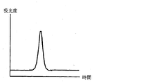
- FIG. It is the block diagram which showed an example of the atomization part periphery of the atomic absorption analyzer shown in FIG. It is a graph which shows the example of a measurement result display of an atomic absorption method analysis. It is a flowchart which shows the flow of the analysis operation
- FIG. 1 is a schematic configuration diagram of an elemental analyzer (plasma emission spectroscopic atomic absorption spectrometer) 100 that performs atomic absorption analysis according to an embodiment of the present invention.
- elemental analyzer plasma emission spectroscopic atomic absorption spectrometer
- the elemental analysis apparatus includes a liquid sending unit 101, a channel 102, an atomization unit 103, a power supply device 104, an optical fiber 105, a spectroscope 106, a detector 107, a computer 108, and a light source 109.
- An optical absorption analysis unit is formed by the optical fiber 105, the spectroscope 106, the detector 107, and the computer (operation control / analysis unit) 108.
- Two electrodes 118 are installed in the middle of the flow path 102, the atomization unit 103 is positioned between the two electrodes 118, and plasma 110 is generated.
- the liquid sample is fed from the liquid feeding unit 101 to the atomization unit 103 via the flow path 102, reaches the waste liquid unit 119 from the atomization unit 103, and is discharged as waste liquid.
- the channel 102 is made of, for example, quartz glass having a diameter of 100 ⁇ m.
- the light 112 from the light source 109 passes through the sample located in the atomization unit 103, and the transmitted light 111 is received by the optical fiber 105 and guided to the spectrometer 106.
- the light separated by the spectroscope 106 is detected by the detector 107.
- the light source 109 may be a holo cathode lamp, deuterium lamp, tungsten iodine lamp, xenon lamp, light emitting diode, or the like.
- the computer 108 is connected to the liquid feeding unit 101, the power supply device 104, the spectroscope 106, and the detector 107, and sends control signals 113, 114, 115, 116, and 117 to control each device. In addition, the computer 108 analyzes the measurement sample based on the light detected by the detector 107.
- FIG. 2 is a diagram showing details of the atomization unit 103 shown in FIG.
- the sample fed to the liquid feeding part 101 or the flow path 102 shown in FIG. 1 fills the flow path of the atomization part 103.
- An electrode 118 formed of Pt or the like provided in the flow path 102 is connected to the power supply device 104 and the computer 108 in FIG.
- the voltage (for example, 2.5 kV) applied to the electrode 118 by the power supply device 104 and the voltage application time are controlled by the control signal 114 from the computer 108.
- the light 111 that has passed through the plasma 110 is guided to the spectroscope 106 by the optical fiber 105 and dispersed, and the detector 107 can detect the light to perform elemental analysis of the sample solution.
- a condensing lens or the like may be used without using the optical fiber 105.
- each apparatus is controlled by the computer 108, and apparatus conditions are input and analysis results are displayed by an input unit (such as a keyboard) and a display unit of the computer 108.
- FIG. 3 shows an image of the analysis result, which is an example that can be displayed on the display unit of the computer 108.
- the vertical axis in FIG. 3 indicates absorbance (abs), and the horizontal axis indicates time (for example, in seconds).
- the principle of elemental analysis according to the present invention is that when a plasma is generated between the electrodes 118, the element contained in the sample is excited and atomized by the plasma, and when the atomized element is irradiated with light, light of a specific wavelength is resonantly absorbed. By measuring this light, the element in the sample is identified and quantified.
- FIG. 4 is an operation flowchart of a measurement method using an atomic absorption method in one embodiment.
- the operator first activates the analyzer (step 201).
- the sample is injected into the liquid feeding unit 101 (for example, a syringe pump) and fed to the flow path 102 at a constant flow rate (for example, 1 ml / min) (step 202).
- a control signal 114 is sent from the computer 108 to the power supply device 104, and a voltage is applied to the electrode 118 (step 203).
- the light 111 from the light source 109 irradiated and transmitted from the light source 109 (for example, a holo-cathode lamp) to the atomizing unit 103 is received by the optical fiber 105 and dispersed by the spectroscope 106 (step 205).
- the dispersed light quantity is detected by the detector 107 (step 206).
- the absorbance is obtained from the amount of light detected by the detector 107 by the computer 108 and displayed (step 207). Note that the absorbance can be continuously measured by applying a voltage multiple times through the electrode 118.
- Whether or not the sample is atomized by the atomization unit 103 can be determined based on whether or not an absorbance peak is detected as shown in FIG. This is because the absorbance peak is not detected unless the sample is atomized.
- whether or not bubbles are generated in the sample can be determined by monitoring the current between the electrodes 118. This is because when bubbles are generated, the current between the electrodes 118 decreases rapidly.
- the sample river water used here is prepared in advance in a 0.1 M nitric acid solution.
- the acid used for analyzing the sample is not limited to nitric acid or a concentration of 0.1M.
- the measurer inputs measurement conditions such as voltage and liquid feeding speed to the computer 108.
- Each unit of the analysis apparatus 100 receives the control signal from the computer 108 and sets measurement conditions.
- the measurement condition setting is completed, a message to that effect is displayed on the display unit of the computer 108 or the like.
- the atomization unit 103 positioned between the two electrodes 118 is irradiated with liquid feeding, application, or light from the light source.
- the solution sample such as river water (prepared) is injected into the liquid feeding unit 101 to perform liquid feeding.
- the measurer starts liquid feeding at a constant flow rate manually or by a control command from the computer 108.
- a solution sample such as river water sent at a constant flow rate fills the atomization unit 103 through the flow path 102.
- the liquid feeding unit 101 When further liquid feeding is performed by the liquid feeding unit 101, the liquid is discharged from the waste liquid unit 119 through the flow path 102.
- a voltage is applied to the atomization unit 103 from the two electrodes 118.
- the voltage application is controlled manually or by the computer 108. Examples of the voltage application conditions include voltage value, application time, application interval (pulse voltage application interval), and the like.
- the light 111 that has passed through the flow path 102 and the sample is received by the optical fiber 105, guided to the spectroscope 106, dispersed, and detected by the detector 107.
- elemental analysis can be performed by monitoring light of a specific wavelength.
- a calibration curve is created from the absorbance obtained by measuring the sample not containing Cd and the sample containing a known amount of Cd by the methods (1) to (6) above, and analyzing the river water By comparing the obtained absorbance, Cd can be quantitatively analyzed.
- plasma can be formed without using a gas. Therefore, the gas supply means and the gas leakage countermeasure of the gas supply means are unnecessary, and the size and weight can be reduced.
- An elemental analysis apparatus and method capable of performing atomic absorption analysis by a possible electric heating method can be realized.
- the light source 109 includes a plurality of types of lamps such as a holocathode lamp, a deuterium lamp, a tungsten iodine lamp, a xenon lamp, and a light emitting diode.
- a holocathode lamp such as a holocathode lamp, a deuterium lamp, a tungsten iodine lamp, a xenon lamp, and a light emitting diode.
- One of the lamps can also be driven. Thereby, a plurality of kinds of elements can be measured by one analyzer.
- the liquid sample is discarded in the waste liquid unit 119.
- a flow path for returning the sample from the waste liquid unit 119 to the liquid feeding unit 101 is provided, atomization is performed again, and the sample It is also possible to carry out the analysis and then drain it.
- the channel 102 is a transparent material resistant to acidity, and any material other than quartz glass can be used as long as the sample does not have metal contamination.
- a silicon tube can be used as the flow path 102.
- DESCRIPTION OF SYMBOLS 100 ... Plasma emission spectroscopy / atomic absorption analyzer, 101 ... Liquid feeding part, 102 ... Flow path, 103 ... Atomization part, 104 ... Power supply device, 105 ... Optical fiber, 106 ⁇ ⁇ ⁇ Spectroscope, 107 ... Detector, 108 ... Computer, 109 ... Light source, 110 ... Plasma, 111 ... Light that has passed through the sample, 112 ... Light from the light source, 113, 114, 115, 116, 117 ... control signal, 118 ... electrode, 119 ... waste liquid part
Landscapes
- Physics & Mathematics (AREA)
- Spectroscopy & Molecular Physics (AREA)
- Health & Medical Sciences (AREA)
- Life Sciences & Earth Sciences (AREA)
- Chemical & Material Sciences (AREA)
- Analytical Chemistry (AREA)
- Biochemistry (AREA)
- General Health & Medical Sciences (AREA)
- General Physics & Mathematics (AREA)
- Immunology (AREA)
- Pathology (AREA)
- Investigating Or Analysing Materials By Optical Means (AREA)
Abstract
Description
Claims (10)
- 測定試料を原子化する原子化部(103)と、
上記原子化部(103)に配置された2つの電極(118)と、
上記2つの電極(118)に電圧を印加し、上記原子化部(103)内に位置する測定試料中にプラズマを発生させる電源部(104)と、
上記原子化部(103)に光を照射する光源(109)と、
上記原子化部(103)に位置する測定試料中に発生したプラズマを通過した上記光源(109)からの光を検出し、測定試料の原子吸光を分析する原子吸光分析部(105~108)と、
を備えることを特徴とする原子吸光元素分析装置。 - 請求項1記載の原子吸光元素分析装置において、上記原子吸光分析部(105~108)は、上記測定試料中に発生したプラズマを通過した上記光源(109)からの光を分光する分光器(106)と、この分光器(106)により分光された光を検出する検出器(107)とを備えることを特徴とする原子吸光元素分析装置。
- 請求項2記載の原子吸光元素分析装置において、上記原子化部(103)に接続された流路(102)と、この流路(102)を介して上記原子化部(103)に分測定試料を送液する送液部(101)とを、さらに備えることを特徴とする原子吸光元素分析装置。
- 請求項3記載の原子吸光元素分析装置において、上記原子吸光分析部(105~108)は、上記検出器(107)により検出された光を分析するともに、上記電源部(104)、上記光源(109)、上記送液部(101)の動作を制御する動作制御・分析部(108)を有することを特徴とする原子吸光元素分析装置。
- 請求項4記載の原子吸光元素分析装置において、上記光源(109)は、複数種類の光源ランプを有し、上記動作制御・分析部(108)により、複数種類の光源ランプのうちの一つが選択され、光を発生させることを特徴とする原子吸光元素分析装置。
- 請求項5記載の原子吸光元素分析装置において、上記複数種類の光源ランプは、ホロカソードランプ、重水素ランプ、タングステンヨウ素ランプ、キセノンランプ、発光ダイオードであることを特徴とする原子吸光元素分析装置。
- 測定試料を2つの電極(118)間に配置し、上記2つの電極(118)に電圧を印加して、測定試料中にプラズマを発生させ、
発生したプラズマに光源(109)からの光を照射し、
測定試料中に発生したプラズマを通過した上記光源(109)からの光を検出し、測定試料の原子吸光を分析することを特徴とする原子吸光元素分析方法。 - 請求項7記載の原子吸光元素分析方法において、上記試料中に発生したプラズマを通過した上記光源(109)からの光を分光し、分光した光を検出して測定試料の原子吸光を分析することを特徴とする原子吸光元素分析方法。
- 請求項8記載の原子吸光元素分析方法において、上記光源(109)は、複数種類の光源ランプを有し、複数種類の光源ランプのうちの一つが選択され、光を発生させることを特徴とする原子吸光元素分析方法。
- 請求項9記載の原子吸光元素分析方法において、上記複数種類の光源ランプは、ホロカソードランプ、重水素ランプ、タングステンヨウ素ランプ、キセノンランプ、発光ダイオードであることを特徴とする原子吸光元素分析方法。
Priority Applications (2)
| Application Number | Priority Date | Filing Date | Title |
|---|---|---|---|
| US13/638,186 US20130201477A1 (en) | 2010-04-12 | 2011-03-25 | Elementary analysis apparatus and method |
| CN2011800185303A CN102834708A (zh) | 2010-04-12 | 2011-03-25 | 元素分析装置以及方法 |
Applications Claiming Priority (2)
| Application Number | Priority Date | Filing Date | Title |
|---|---|---|---|
| JP2010091371A JP5343033B2 (ja) | 2010-04-12 | 2010-04-12 | 元素分析装置及び方法 |
| JP2010-091371 | 2010-04-12 |
Publications (1)
| Publication Number | Publication Date |
|---|---|
| WO2011129189A1 true WO2011129189A1 (ja) | 2011-10-20 |
Family
ID=44798567
Family Applications (1)
| Application Number | Title | Priority Date | Filing Date |
|---|---|---|---|
| PCT/JP2011/057319 Ceased WO2011129189A1 (ja) | 2010-04-12 | 2011-03-25 | 元素分析装置及び方法 |
Country Status (4)
| Country | Link |
|---|---|
| US (1) | US20130201477A1 (ja) |
| JP (1) | JP5343033B2 (ja) |
| CN (1) | CN102834708A (ja) |
| WO (1) | WO2011129189A1 (ja) |
Families Citing this family (5)
| Publication number | Priority date | Publication date | Assignee | Title |
|---|---|---|---|---|
| EP3045895A1 (en) * | 2015-01-13 | 2016-07-20 | ARKRAY, Inc. | Plasma spectrochemical analysis method and plasma spectrochemical analyzer |
| JP7211616B2 (ja) * | 2018-03-29 | 2023-01-24 | 株式会社日立ハイテクサイエンス | 原子吸光光度計における極微量分析診断方法 |
| DE102019103035A1 (de) * | 2019-02-07 | 2020-08-13 | Analytik Jena Ag | Atomabsorptionsspektrometer |
| CN113720811B (zh) * | 2021-08-19 | 2022-12-30 | 中国地质大学(武汉) | 一种基于超声雾化进样的微等离子体激发源及激发方法 |
| CN113791053B (zh) * | 2021-09-13 | 2022-12-23 | 浙江大学 | 电势扫描局域表面等离子体共振的传感检测装置及方法 |
Citations (3)
| Publication number | Priority date | Publication date | Assignee | Title |
|---|---|---|---|---|
| JPH0643094A (ja) * | 1992-07-22 | 1994-02-18 | Shimadzu Corp | 原子吸光分光光度計 |
| JPH07128228A (ja) * | 1993-10-29 | 1995-05-19 | Shimadzu Corp | 原子吸光分光光度計 |
| JPH08201282A (ja) * | 1995-01-23 | 1996-08-09 | Hitachi Ltd | フレームレス原子吸光用原子化装置 |
Family Cites Families (7)
| Publication number | Priority date | Publication date | Assignee | Title |
|---|---|---|---|---|
| DE3720376A1 (de) * | 1987-06-19 | 1988-12-29 | Bodenseewerk Perkin Elmer Co | Ofen zur elektrothermischen atomisierung fuer die atomabsorptions-spektroskopie |
| US5081397A (en) * | 1989-07-11 | 1992-01-14 | University Of British Columbia | Atmospheric pressure capacitively coupled plasma atomizer for atomic absorption and source for atomic emission spectroscopy |
| US5880823A (en) * | 1994-06-10 | 1999-03-09 | Lu; Chih-Shun | Method and apparatus for measuring atomic vapor density in deposition systems |
| US6741345B2 (en) * | 2001-02-08 | 2004-05-25 | National Research Council Of Canada | Method and apparatus for in-process liquid analysis by laser induced plasma spectroscopy |
| CN2821568Y (zh) * | 2005-09-14 | 2006-09-27 | 北京普析通用仪器有限责任公司 | 多通道无火焰原子吸收分析仪 |
| CN101482497B (zh) * | 2009-02-19 | 2010-10-27 | 成都理工大学 | 在线电化学分离富集钨丝电热原子吸收检测装置 |
| CN101692041B (zh) * | 2009-04-02 | 2013-01-23 | 马怡载 | 多元素测定用金属钨或钽平台石墨管原子吸收光度计 |
-
2010
- 2010-04-12 JP JP2010091371A patent/JP5343033B2/ja not_active Expired - Fee Related
-
2011
- 2011-03-25 US US13/638,186 patent/US20130201477A1/en not_active Abandoned
- 2011-03-25 CN CN2011800185303A patent/CN102834708A/zh active Pending
- 2011-03-25 WO PCT/JP2011/057319 patent/WO2011129189A1/ja not_active Ceased
Patent Citations (3)
| Publication number | Priority date | Publication date | Assignee | Title |
|---|---|---|---|---|
| JPH0643094A (ja) * | 1992-07-22 | 1994-02-18 | Shimadzu Corp | 原子吸光分光光度計 |
| JPH07128228A (ja) * | 1993-10-29 | 1995-05-19 | Shimadzu Corp | 原子吸光分光光度計 |
| JPH08201282A (ja) * | 1995-01-23 | 1996-08-09 | Hitachi Ltd | フレームレス原子吸光用原子化装置 |
Also Published As
| Publication number | Publication date |
|---|---|
| US20130201477A1 (en) | 2013-08-08 |
| JP5343033B2 (ja) | 2013-11-13 |
| JP2011220884A (ja) | 2011-11-04 |
| CN102834708A (zh) | 2012-12-19 |
Similar Documents
| Publication | Publication Date | Title |
|---|---|---|
| US6012326A (en) | Detection of volatile substances | |
| KR101410526B1 (ko) | 금속시료 중의 유황의 분석방법 및 분석장치 | |
| JP5343033B2 (ja) | 元素分析装置及び方法 | |
| JP2012508890A (ja) | サンプルまたはサンプル成分の分析システム、およびこのシステムの製造方法および使用方法 | |
| JP5987968B2 (ja) | 放電イオン化電流検出器及びその調整方法 | |
| JP2016206051A (ja) | 光学分析装置 | |
| Matusiewicz et al. | Simultaneous determination of As, Bi, Sb, Se and Sn by microwave induced plasma spectrometry using a quadruple-mode microflow ultrasonic nebulizer for in situ hydride generation with internal standardization | |
| CN102121902A (zh) | 一种在线拉曼光谱仪校正装置及其校正方法 | |
| Yu et al. | Iodine excitation in a dielectric barrier discharge micro-plasma and its determination by optical emission spectrometry | |
| KR20150051579A (ko) | 레이저 유도 플라즈마 분광 분석장치 | |
| US8913240B2 (en) | Fluorescence spectrophotometer | |
| EP0015284B1 (en) | Flameless emission spectroscope apparatus and sample introduction method for same | |
| US9784616B2 (en) | Spectrophotometer | |
| US20170322147A1 (en) | Atomic absorption photometer and atomic absorption measurement method | |
| JP2006281208A (ja) | マイクロ波支援化学反応のための分光器に基づくリアルタイム制御 | |
| Zhang et al. | Stability enhanced online powdery cement raw materials quality monitoring using laser-induced breakdown spectroscopy | |
| Lindner et al. | The influence of laser-particle interaction in laser induced breakdown spectroscopy and laser ablation inductively coupled plasma spectrometry | |
| Matusiewicz et al. | Analytical evaluation of a quadruple-mode micro-flow ultrasonic nebulizer for sample introduction in microwave induced plasma spectrometry | |
| KR101504042B1 (ko) | 광량 분배가 가능한 더블 빔 방식을 이용한 cod 측정 방법 및 장치 | |
| JPWO2012036137A1 (ja) | 分析装置及び分析方法 | |
| Zhang et al. | Plasma-cavity ringdown spectroscopy for analytical measurement: Progress and prospectives | |
| Matusiewicz et al. | Development of interface for online coupling of micro-fluidic chip-based photo-micro-reactor/ultrasonic nebulization with microwave induced plasma spectrometry and its application in simultaneous determination of inorganic trace elements in biological materials | |
| JPH06109639A (ja) | 発光分光分析方法 | |
| Matsui et al. | Signal enhancement by crossing the sample flow at a small angle against the laser beam in multiphoton ionization mass spectrometry | |
| JP7845017B2 (ja) | プラズマを用いた元素分析装置 |
Legal Events
| Date | Code | Title | Description |
|---|---|---|---|
| WWE | Wipo information: entry into national phase |
Ref document number: 201180018530.3 Country of ref document: CN |
|
| 121 | Ep: the epo has been informed by wipo that ep was designated in this application |
Ref document number: 11768710 Country of ref document: EP Kind code of ref document: A1 |
|
| NENP | Non-entry into the national phase |
Ref country code: DE |
|
| WWE | Wipo information: entry into national phase |
Ref document number: 13638186 Country of ref document: US |
|
| 122 | Ep: pct application non-entry in european phase |
Ref document number: 11768710 Country of ref document: EP Kind code of ref document: A1 |