WO2011125984A1 - 液晶配向剤、液晶配向膜及び液晶表示素子 - Google Patents
液晶配向剤、液晶配向膜及び液晶表示素子 Download PDFInfo
- Publication number
- WO2011125984A1 WO2011125984A1 PCT/JP2011/058553 JP2011058553W WO2011125984A1 WO 2011125984 A1 WO2011125984 A1 WO 2011125984A1 JP 2011058553 W JP2011058553 W JP 2011058553W WO 2011125984 A1 WO2011125984 A1 WO 2011125984A1
- Authority
- WO
- WIPO (PCT)
- Prior art keywords
- liquid crystal
- formula
- aligning agent
- alkoxysilane
- polysiloxane
- Prior art date
- Legal status (The legal status is an assumption and is not a legal conclusion. Google has not performed a legal analysis and makes no representation as to the accuracy of the status listed.)
- Ceased
Links
Classifications
-
- C—CHEMISTRY; METALLURGY
- C08—ORGANIC MACROMOLECULAR COMPOUNDS; THEIR PREPARATION OR CHEMICAL WORKING-UP; COMPOSITIONS BASED THEREON
- C08G—MACROMOLECULAR COMPOUNDS OBTAINED OTHERWISE THAN BY REACTIONS ONLY INVOLVING UNSATURATED CARBON-TO-CARBON BONDS
- C08G73/00—Macromolecular compounds obtained by reactions forming a linkage containing nitrogen with or without oxygen or carbon in the main chain of the macromolecule, not provided for in groups C08G12/00 - C08G71/00
- C08G73/06—Polycondensates having nitrogen-containing heterocyclic rings in the main chain of the macromolecule
- C08G73/10—Polyimides; Polyester-imides; Polyamide-imides; Polyamide acids or similar polyimide precursors
-
- C—CHEMISTRY; METALLURGY
- C08—ORGANIC MACROMOLECULAR COMPOUNDS; THEIR PREPARATION OR CHEMICAL WORKING-UP; COMPOSITIONS BASED THEREON
- C08L—COMPOSITIONS OF MACROMOLECULAR COMPOUNDS
- C08L79/00—Compositions of macromolecular compounds obtained by reactions forming in the main chain of the macromolecule a linkage containing nitrogen with or without oxygen or carbon only, not provided for in groups C08L61/00 - C08L77/00
- C08L79/04—Polycondensates having nitrogen-containing heterocyclic rings in the main chain; Polyhydrazides; Polyamide acids or similar polyimide precursors
- C08L79/08—Polyimides; Polyester-imides; Polyamide-imides; Polyamide acids or similar polyimide precursors
-
- C—CHEMISTRY; METALLURGY
- C09—DYES; PAINTS; POLISHES; NATURAL RESINS; ADHESIVES; COMPOSITIONS NOT OTHERWISE PROVIDED FOR; APPLICATIONS OF MATERIALS NOT OTHERWISE PROVIDED FOR
- C09K—MATERIALS FOR MISCELLANEOUS APPLICATIONS, NOT PROVIDED FOR ELSEWHERE
- C09K19/00—Liquid crystal materials
- C09K19/52—Liquid crystal materials characterised by components which are not liquid crystals, e.g. additives with special physical aspect: solvents, solid particles
- C09K19/54—Additives having no specific mesophase characterised by their chemical composition
- C09K19/56—Aligning agents
-
- G—PHYSICS
- G02—OPTICS
- G02F—OPTICAL DEVICES OR ARRANGEMENTS FOR THE CONTROL OF LIGHT BY MODIFICATION OF THE OPTICAL PROPERTIES OF THE MEDIA OF THE ELEMENTS INVOLVED THEREIN; NON-LINEAR OPTICS; FREQUENCY-CHANGING OF LIGHT; OPTICAL LOGIC ELEMENTS; OPTICAL ANALOGUE/DIGITAL CONVERTERS
- G02F1/00—Devices or arrangements for the control of the intensity, colour, phase, polarisation or direction of light arriving from an independent light source, e.g. switching, gating or modulating; Non-linear optics
- G02F1/01—Devices or arrangements for the control of the intensity, colour, phase, polarisation or direction of light arriving from an independent light source, e.g. switching, gating or modulating; Non-linear optics for the control of the intensity, phase, polarisation or colour
- G02F1/13—Devices or arrangements for the control of the intensity, colour, phase, polarisation or direction of light arriving from an independent light source, e.g. switching, gating or modulating; Non-linear optics for the control of the intensity, phase, polarisation or colour based on liquid crystals, e.g. single liquid crystal display cells
- G02F1/133—Constructional arrangements; Operation of liquid crystal cells; Circuit arrangements
- G02F1/1333—Constructional arrangements; Manufacturing methods
- G02F1/1337—Surface-induced orientation of the liquid crystal molecules, e.g. by alignment layers
-
- G—PHYSICS
- G02—OPTICS
- G02F—OPTICAL DEVICES OR ARRANGEMENTS FOR THE CONTROL OF LIGHT BY MODIFICATION OF THE OPTICAL PROPERTIES OF THE MEDIA OF THE ELEMENTS INVOLVED THEREIN; NON-LINEAR OPTICS; FREQUENCY-CHANGING OF LIGHT; OPTICAL LOGIC ELEMENTS; OPTICAL ANALOGUE/DIGITAL CONVERTERS
- G02F1/00—Devices or arrangements for the control of the intensity, colour, phase, polarisation or direction of light arriving from an independent light source, e.g. switching, gating or modulating; Non-linear optics
- G02F1/01—Devices or arrangements for the control of the intensity, colour, phase, polarisation or direction of light arriving from an independent light source, e.g. switching, gating or modulating; Non-linear optics for the control of the intensity, phase, polarisation or colour
- G02F1/13—Devices or arrangements for the control of the intensity, colour, phase, polarisation or direction of light arriving from an independent light source, e.g. switching, gating or modulating; Non-linear optics for the control of the intensity, phase, polarisation or colour based on liquid crystals, e.g. single liquid crystal display cells
- G02F1/133—Constructional arrangements; Operation of liquid crystal cells; Circuit arrangements
- G02F1/1333—Constructional arrangements; Manufacturing methods
- G02F1/1337—Surface-induced orientation of the liquid crystal molecules, e.g. by alignment layers
- G02F1/133711—Surface-induced orientation of the liquid crystal molecules, e.g. by alignment layers by organic films, e.g. polymeric films
- G02F1/133719—Surface-induced orientation of the liquid crystal molecules, e.g. by alignment layers by organic films, e.g. polymeric films with coupling agent molecules, e.g. silane
-
- G—PHYSICS
- G02—OPTICS
- G02F—OPTICAL DEVICES OR ARRANGEMENTS FOR THE CONTROL OF LIGHT BY MODIFICATION OF THE OPTICAL PROPERTIES OF THE MEDIA OF THE ELEMENTS INVOLVED THEREIN; NON-LINEAR OPTICS; FREQUENCY-CHANGING OF LIGHT; OPTICAL LOGIC ELEMENTS; OPTICAL ANALOGUE/DIGITAL CONVERTERS
- G02F1/00—Devices or arrangements for the control of the intensity, colour, phase, polarisation or direction of light arriving from an independent light source, e.g. switching, gating or modulating; Non-linear optics
- G02F1/01—Devices or arrangements for the control of the intensity, colour, phase, polarisation or direction of light arriving from an independent light source, e.g. switching, gating or modulating; Non-linear optics for the control of the intensity, phase, polarisation or colour
- G02F1/13—Devices or arrangements for the control of the intensity, colour, phase, polarisation or direction of light arriving from an independent light source, e.g. switching, gating or modulating; Non-linear optics for the control of the intensity, phase, polarisation or colour based on liquid crystals, e.g. single liquid crystal display cells
- G02F1/133—Constructional arrangements; Operation of liquid crystal cells; Circuit arrangements
- G02F1/1333—Constructional arrangements; Manufacturing methods
- G02F1/1337—Surface-induced orientation of the liquid crystal molecules, e.g. by alignment layers
- G02F1/133711—Surface-induced orientation of the liquid crystal molecules, e.g. by alignment layers by organic films, e.g. polymeric films
- G02F1/133715—Surface-induced orientation of the liquid crystal molecules, e.g. by alignment layers by organic films, e.g. polymeric films by first depositing a monomer
-
- G—PHYSICS
- G02—OPTICS
- G02F—OPTICAL DEVICES OR ARRANGEMENTS FOR THE CONTROL OF LIGHT BY MODIFICATION OF THE OPTICAL PROPERTIES OF THE MEDIA OF THE ELEMENTS INVOLVED THEREIN; NON-LINEAR OPTICS; FREQUENCY-CHANGING OF LIGHT; OPTICAL LOGIC ELEMENTS; OPTICAL ANALOGUE/DIGITAL CONVERTERS
- G02F1/00—Devices or arrangements for the control of the intensity, colour, phase, polarisation or direction of light arriving from an independent light source, e.g. switching, gating or modulating; Non-linear optics
- G02F1/01—Devices or arrangements for the control of the intensity, colour, phase, polarisation or direction of light arriving from an independent light source, e.g. switching, gating or modulating; Non-linear optics for the control of the intensity, phase, polarisation or colour
- G02F1/13—Devices or arrangements for the control of the intensity, colour, phase, polarisation or direction of light arriving from an independent light source, e.g. switching, gating or modulating; Non-linear optics for the control of the intensity, phase, polarisation or colour based on liquid crystals, e.g. single liquid crystal display cells
- G02F1/133—Constructional arrangements; Operation of liquid crystal cells; Circuit arrangements
- G02F1/1333—Constructional arrangements; Manufacturing methods
- G02F1/1337—Surface-induced orientation of the liquid crystal molecules, e.g. by alignment layers
- G02F1/133742—Surface-induced orientation of the liquid crystal molecules, e.g. by alignment layers for homeotropic alignment
Definitions
- the present invention relates to a liquid crystal alignment agent containing polysiloxane obtained by polycondensation of alkoxysilane, a liquid crystal alignment film obtained from the liquid crystal alignment agent, and a liquid crystal display element having the liquid crystal alignment film.
- VA liquid crystal display elements are widely used for large-screen liquid crystal televisions and high-definition mobile applications (display units of digital cameras and mobile phones).
- the VA method includes an MVA method (Multi Vertical Alignment) in which protrusions for controlling the direction in which the liquid crystal is tilted are formed on the TFT substrate or the color filter substrate, and a direction in which the liquid crystal is tilted by forming an slit in the ITO electrode of the substrate.
- MVA method Multi Vertical Alignment
- a PVA (Paterned Vertical Alignment) system to be controlled is known.
- PSA Polymer Sustained Alignment
- the PSA system is a technology that has attracted attention in recent years.
- a photopolymerizable compound is usually added to a liquid crystal, and after producing a liquid crystal panel, an electric field is applied to irradiate the liquid crystal with ultraviolet rays (UV) while the liquid crystal is tilted.
- UV ultraviolet rays
- the polymerizable compound is photopolymerized to fix the alignment direction of the liquid crystal, causing a pretilt and improving the response speed.
- a slit is formed in one electrode constituting the liquid crystal panel, and the electrode pattern on the opposite side can operate even in a structure in which no protrusion in the MVA method or a slit in the PVA method is provided. It has features that simplification of production and excellent panel transmittance can be obtained (see Patent Document 1).
- inorganic liquid crystal alignment film materials are also known along with conventionally used organic liquid crystal alignment film materials such as polyimide.
- a composition containing a reaction product of tetraalkoxysilane, trialkoxysilane, alcohol, and oxalic acid is used as a material for a coating-type inorganic alignment film, and is vertically aligned on an electrode substrate of a liquid crystal display element. It has been reported that a liquid crystal alignment film having excellent alignment properties, heat resistance and uniformity is formed (see Patent Document 2).
- liquid crystal aligning agent composition containing a tetraalkoxysilane, a specific trialkoxysilane and a reaction product with water, and a specific glycol ether solvent, display defects can be prevented and even after long-time driving. It has been reported that a liquid crystal alignment film is formed without leaving an afterimage, without reducing the ability to align liquid crystal, and with little reduction in voltage holding ratio against light and heat. (See Patent Document 3)
- JP 2004-302061 A JP 09-281502 A JP 2005-250244 A
- the object of the present invention is to improve the response speed and achieve good alignment even when the amount of the polymerizable compound added to the liquid crystal in the PSA method is small, and even when the liquid crystal without adding the polymerizable compound is used.
- An object of the present invention is to provide a liquid crystal aligning agent for a liquid crystal display element, a liquid crystal aligning film obtained from the liquid crystal aligning agent, and a liquid crystal display element having the liquid crystal aligning film capable of obtaining a state.
- a liquid crystal aligning agent for a device comprising polysiloxane obtained by polycondensation of an alkoxysilane represented by the formula (1) and an alkoxysilane containing the alkoxysilane represented by the formula (2) .
- R 1 Si (OR 2 ) 3 (1) R 1 is a hydrocarbon group having 8 to 30 carbon atoms which may be substituted with a fluorine atom, and R 2 represents an alkyl group having 1 to 5 carbon atoms.
- R 3 represents a hydrocarbon group having 1 to 18 carbon atoms
- R 4 represents an alkyl group having 1 to 5 carbon atoms.
- polysiloxane according to any one of [1] to [3], wherein the polysiloxane is a polysiloxane obtained by polycondensation of an alkoxysilane containing an alkoxysilane represented by the following formula (4): Liquid crystal aligning agent.
- R 5 is a hydrogen atom or a hydrocarbon group having 1 to 6 carbon atoms which may be substituted with a hetero atom, a halogen atom, an amino group, a glycidoxy group, a mercapto group, an isocyanate group or a ureido group
- R 6 represents an alkyl group having 1 to 5 carbon atoms
- n represents an integer of 0 to 3.
- the polysiloxane contains 0.1 to 30 mol% of the alkoxysilane represented by the formula (1) in all alkoxysilanes, and the alkoxysilane represented by the formula (2) in all alkoxysilanes.
- the liquid crystal aligning agent according to any one of [1] to [8] is applied, and UV is irradiated in a state where a voltage is applied to a liquid crystal cell in which the liquid crystal is sandwiched between two baked substrates. Liquid crystal display element.
- liquid crystal aligning agent of the present invention even when the amount of the polymerizable compound added to the liquid crystal in the PSA method is small, or when using the liquid crystal without adding the polymerizable compound, the response speed is improved and good.
- a liquid crystal alignment film for a liquid crystal display element capable of obtaining an alignment state and a display element having the liquid crystal alignment film are obtained.
- the present invention is a liquid crystal aligning agent for PSA system containing a polysiloxane obtained by polycondensation of an alkoxysilane represented by the formula (1) and an alkoxysilane containing the alkoxysilane represented by the formula (2).
- R 1 Si (OR 2 ) 3 (1)
- R 1 is a hydrocarbon group having 8 to 30 carbon atoms which may be substituted with a fluorine atom, and R 2 represents an alkyl group having 1 to 5 carbon atoms.
- “may be substituted” means “substituted or not substituted”.
- R 3 represents a hydrocarbon group having 1 to 18 carbon atoms
- R 4 represents an alkyl group having 1 to 5 carbon atoms.
- R 1 (hereinafter also referred to as a specific organic group) of the alkoxysilane represented by the formula (1) is a hydrocarbon group having 8 to 30 carbon atoms, preferably 8 to 22 carbon atoms which may be substituted with fluorine. There is no particular limitation as long as it has the effect of vertically aligning the liquid crystal. Examples thereof include an alkyl group, a fluoroalkyl group, an alkenyl group, a phenethyl group, a styrylalkyl group, a naphthyl group, and a fluorophenylalkyl group.
- alkoxysilanes in which R 1 is an alkyl group or a fluoroalkyl group are preferable because they are relatively inexpensive and easily available as commercial products.
- alkoxysilane in which R 1 is an alkyl group is preferable.
- the polysiloxane used in the present invention may have a plurality of these specific organic groups.
- R 2 of the alkoxysilane represented by the formula (1) is an alkyl group having 1 to 5 carbon atoms, preferably 1 to 3 carbon atoms. More preferably, R 2 is a methyl group or an ethyl group. Although the specific example of the alkoxysilane represented by this Formula (1) is given, it is not limited to this.
- octyltrimethoxysilane, octyltriethoxysilane, decyltrimethoxysilane, decyltriethoxysilane, dodecyltrimethoxysilane, dodecyltriethoxysilane, hexadecyltrimethoxysilane, hexadecyltriethoxysilane, heptadecyltrimethoxysilane Heptadecyltriethoxysilane, octadecyltrimethoxysilane, octadecyltriethoxysilane, nonadecyltrimethoxysilane, nonadecyltriethoxysilane, undecyltriethoxysilane, or undecyltrimethoxysilane is preferred.
- the above-mentioned alkoxysilane represented by the formula (1) having a specific organic group is preferably 0.1 mol% or more in order to obtain good liquid crystal alignment in all alkoxysilanes used for obtaining polysiloxane. More preferably, it is 0.5 mol% or more. More preferably, it is 1 mol% or more. Further, in order to obtain sufficient curing characteristics of the liquid crystal alignment film to be formed, 30 mol% or less is preferable. More preferably, it is 22 mol% or less.
- R 3 of the alkoxysilane represented by the formula (2) is a hydrocarbon group having 1 to 18 carbon atoms, preferably 1 to 12 carbon atoms. Hydrogen; ring structures such as aliphatic ring, aromatic ring and hetero ring; and hetero atoms such as oxygen atom, nitrogen atom and sulfur atom may be contained.
- An alkylene group and a phenylene group are preferred.
- the alkylene group has 1 to 18 carbon atoms, more preferably 1 to 12 carbon atoms.
- the phenylene group is represented by the following formula (3), and m and n are each an integer of 0 to 6, preferably an integer of 0 to 2.
- R 4 of the alkoxysilane represented by the formula (2) is the same as the definition of R 2 in the above formula (1), and a preferable group of R 4 is the same as that of R 2 .
- alkoxysilane represented by Formula (2) is not limited to these.
- the alkoxysilane represented by the formula (2) having two specific organic groups is preferably 3 mol% or more in all alkoxysilanes used for obtaining the polysiloxane. More preferably, it is 5 mol% or more. More preferably, it is 10 mol% or more. Moreover, in order to fully harden the liquid crystal aligning film formed, 70 mol% or less is preferable.
- the alkoxysilane represented by the formula (1) is preferably contained in the total alkoxysilane used in an amount of 0.1 to 30 mol%, particularly preferably 2 to 20 mol%, and the formula (2) Is preferably 3 to 70 mol%, particularly preferably 5 to 30 mol%, based on the total alkoxy silane used.
- the alkoxysilane represented by following formula (4) can also be used besides the alkoxysilane represented by Formula (1) and Formula (2). Since the alkoxysilane represented by the formula (4) can impart various properties to the polysiloxane, one or more types can be selected and used according to the required properties.
- R 5 is a hydrogen atom or a hydrocarbon group having 1 to 6 carbon atoms which may be substituted with a hetero atom, a halogen atom, an amino group, a glycidoxy group, a mercapto group, an isocyanate group or a ureido group.
- R 6 represents an alkyl group having 1 to 5 carbon atoms, preferably 1 to 3 carbon atoms, and n represents an integer of 0 to 3, preferably 0 to 2.
- R 5 of the alkoxysilane represented by the formula (4) is a hydrogen atom or an organic group having 1 to 6 carbon atoms (hereinafter also referred to as a third organic group).
- third organic groups include aliphatic hydrocarbons; ring structures such as aliphatic rings, aromatic rings, and heterocycles; unsaturated bonds; heteroatoms such as oxygen, nitrogen, and sulfur atoms Or an organic group having 1 to 6 carbon atoms, which may have a branched structure. This organic group may be substituted with a halogen atom, amino group, glycidoxy group, mercapto group, isocyanate group, ureido group or the like.
- alkoxysilane represented by Formula (4) is not limited to this.
- specific examples of alkoxysilane when R 5 is a hydrogen atom include trimethoxysilane, triethoxysilane, tripropoxysilane, tributoxysilane and the like.
- alkoxysilane of the formula (4) specific examples of the alkoxysilane when R 5 is a third organic group include methyltrimethoxysilane, methyltriethoxysilane, ethyltrimethoxysilane, ethyltriethoxysilane.
- the polysiloxane used in the present invention is a kind of the alkoxysilane represented by the above formula (4) as long as the effects of the present invention are not impaired for the purpose of improving the adhesion with the substrate and the affinity with the liquid crystal molecules. Or you may have multiple types.
- the alkoxysilane represented by the formula (4) the alkoxysilane in which n is 0 is tetraalkoxysilane. Tetraalkoxysilane is preferable for obtaining the polysiloxane of the present invention because it easily condenses with the alkoxysilane represented by the formulas (1) and (2).
- alkoxysilane in which n is 0 in the formula (4) tetramethoxysilane, tetraethoxysilane, tetrapropoxysilane or tetrabutoxysilane is more preferable, and tetramethoxysilane or tetraethoxysilane is particularly preferable.
- the amount of the alkoxysilane represented by the formula (4) is 10 to 96.9 mol% in the total alkoxysilane used for obtaining the polysiloxane. It is preferable that More preferably, it is 35 to 99.8 mol%.
- the method for obtaining the polysiloxane used in the present invention is not particularly limited. In the present invention, it is obtained by condensing an alkoxysilane having the above-mentioned formulas (1) and (2) as essential components in an organic solvent. Usually, polysiloxane is obtained as a solution obtained by polycondensation of such alkoxysilanes and uniformly dissolved in an organic solvent.
- a method for polycondensation of polysiloxane for example, a method of hydrolyzing and condensing alkoxysilane in a solvent such as alcohol or glycol can be mentioned. At that time, the hydrolysis / condensation reaction may be either partial hydrolysis or complete hydrolysis.
- the amount of water used in the above reaction can be appropriately selected as desired, but it is usually preferably 0.5 to 2.5 times mol of all alkoxy groups in alkoxysilane.
- acids such as hydrochloric acid, sulfuric acid, nitric acid, acetic acid, formic acid, succinic acid, maleic acid and fumaric acid; alkalis such as ammonia, methylamine, ethylamine, ethanolamine and triethylamine
- alkalis such as ammonia, methylamine, ethylamine, ethanolamine and triethylamine
- a metal salt such as hydrochloric acid, sulfuric acid or nitric acid
- a method of heating and polycondensing a mixture of alkoxysilane, a solvent and oxalic acid can be mentioned. Specifically, after adding oxalic acid to alcohol in advance to obtain an alcohol solution of oxalic acid, the alkoxysilane is mixed while the solution is heated. In that case, the amount of succinic acid used is preferably 0.2 to 2 mol with respect to 1 mol of all alkoxy groups of the alkoxysilane. Heating in this method can be performed at a liquid temperature of 50 to 180 ° C. Preferably, it is a method of heating for several tens of minutes to several tens of hours under reflux so that evaporation or volatilization of the liquid does not occur.
- the solvent used for polycondensation of alkoxysilane (hereinafter also referred to as polymerization solvent) is not particularly limited as long as it can dissolve alkoxysilane. Moreover, even when alkoxysilane does not melt
- Such a polymerization solvent include alcohols such as methanol, ethanol, propanol, butanol and diacetone alcohol: ethylene glycol, diethylene glycol, propylene glycol, dipropylene glycol, hexylene glycol, 1,3-propanediol, 1,2-butanediol, 1,3-butanediol, 1,4-butanediol, 2,3-butanediol, 1,2-pentanediol, 1,3-pentanediol, 1,4-pentanediol, 1 , 5-pentanediol, 2,4-pentanediol, 2,3-pentanediol, 1,6-hexanediol, and other glycols: ethylene glycol monomethyl ether, ethylene glycol monoethyl ether, ethylene glycol monopropyl ether Ethylene glycol monobutyl ether
- the polysiloxane polymerization solution (hereinafter also referred to as polymerization solution) obtained by the above method has a concentration obtained by converting silicon atoms of all alkoxysilanes charged as raw materials into SiO 2 (hereinafter referred to as SiO 2 conversion concentration). Is preferably 20% by mass or less, more preferably 5 to 15% by mass. By selecting an arbitrary concentration within this concentration range, gel formation can be suppressed and a homogeneous solution can be obtained.
- the polymerization solution obtained by the above method may be used as a polysiloxane solution as it is, or if necessary, the solution obtained by the above method may be concentrated or diluted by adding a solvent. Or may be substituted with another solvent to form a polysiloxane solution.
- the solvent to be used hereinafter also referred to as additive solvent
- the additive solvent is not particularly limited as long as the polysiloxane is uniformly dissolved, and one kind or plural kinds can be arbitrarily selected and used.
- Such an additive solvent include, in addition to the solvents mentioned as examples of the polymerization solvent described above, ketones such as acetone, methyl ethyl ketone, and methyl isobutyl ketone; esters such as methyl acetate, ethyl acetate, and ethyl lactate. Can be mentioned. These solvents can improve the applicability when the liquid crystal aligning agent is applied onto the substrate by adjusting the viscosity of the liquid crystal aligning agent, or by spin coating, flexographic printing, ink jetting or the like.
- inorganic fine particles fine particles such as silica fine particles, alumina fine particles, titania fine particles, and magnesium fluoride fine particles are preferable, and those in the state of a colloidal solution are particularly preferable.
- This colloidal solution may be a dispersion of inorganic fine particles in a dispersion medium, or a commercially available colloidal solution.
- the surface shape of the formed cured film can be changed or other functions can be imparted.
- the inorganic fine particles preferably have an average particle size of 0.001 to 0.2 ⁇ m, more preferably 0.001 to 0.1 ⁇ m. When the average particle diameter of the inorganic fine particles exceeds 0.2 ⁇ m, the transparency of the cured film formed using the prepared coating liquid may be lowered.
- the dispersion medium for the inorganic fine particles include water and organic solvents.
- the colloidal solution it is preferable that the pH or pKa is adjusted to 1 to 10 from the viewpoint of the stability of the coating solution for forming a film. More preferably, it is 2-7.
- organic solvent used for the dispersion medium of the colloidal solution examples include alcohols such as methanol, propanol, butanol, ethylene glycol, propylene glycol, butanediol, pentanediol, hexylene glycol, diethylene glycol, dipropylene glycol, and ethylene glycol monopropyl ether; Ketones such as methyl ethyl ketone and methyl isobutyl ketone; aromatic hydrocarbons such as toluene and xylene; amides such as dimethylformamide, dimethylacetamide and N-methylpyrrolidone; esters such as ethyl acetate, butyl acetate and ⁇ -butyrolactone; Examples include ethers such as tetrahydrofuran and 1,4-dioxane. Of these, alcohols or ketones are preferred. These organic solvents can be used alone or in admixture of two or more as a dispersion
- metalloxane oligomer and metalloxane polymer single or composite oxide precursors such as silicon, titanium, aluminum, tantalum, antimony, bismuth, tin, indium, and zinc are used.
- the metalloxane oligomer or metalloxane polymer may be a commercially available product or may be obtained from monomers such as metal alkoxides, nitrates, hydrochlorides and carboxylates by a conventional method such as hydrolysis.
- metalloxane oligomers and metalloxane polymers include siloxane oligomers or siloxanes such as methyl silicate 51, methyl silicate 53A, ethyl silicate 40, ethyl silicate 48, EMS-485, and SS-101 manufactured by Colcoat.
- siloxane oligomers or siloxanes such as methyl silicate 51, methyl silicate 53A, ethyl silicate 40, ethyl silicate 48, EMS-485, and SS-101 manufactured by Colcoat.
- titanoxane oligomers such as polymers and titanium-n-butoxide tetramer manufactured by Kanto Chemical Co., Inc. You may use these individually or in mixture of 2 or more types.
- a leveling agent, surfactant, etc. can use a well-known thing, and since a commercial item is easy to acquire especially, it is preferable.
- the method of mixing the above-mentioned other components with polysiloxane may be simultaneous with or after polysiloxane, and is not particularly limited.
- the liquid crystal aligning agent of this invention is the solution containing the polysiloxane mentioned above and other components as needed.
- a solvent selected from the group consisting of the above-mentioned polysiloxane polymerization solvent and additive solvent is used.
- the content of polysiloxane in the liquid crystal aligning agent is preferably 0.5 to 15% by mass, more preferably 1 to 6% by mass in terms of SiO 2 equivalent concentration. Be in the range of such terms of SiO 2 concentration, easy to obtain a desired film thickness by a single coating, easy pot life sufficient solution is obtained.
- the method for preparing the liquid crystal aligning agent of the present invention is not particularly limited.
- the polysiloxane used in the present invention may be in a state where other components added as necessary are uniformly mixed.
- polysiloxane since polysiloxane is polycondensed in a solvent, it is convenient to use the polysiloxane solution as it is or to add other components to the polysiloxane solution as required.
- the most convenient method is to use the polysiloxane polymerization solution as it is.
- the solvent chosen from the group which consists of the polymerization solvent of polysiloxane mentioned above, and an addition solvent can be used.
- the liquid crystal aligning film of this invention is obtained using the liquid crystal aligning agent of this invention.
- the cured film obtained by drying and baking can also be used as a liquid crystal aligning film as it is.
- the cured film is rubbed, irradiated with polarized light or light of a specific wavelength, processed with an ion beam, etc., or irradiated with UV in a state where a voltage is applied to the liquid crystal display element after filling the liquid crystal. It is also possible.
- the liquid crystal aligning agent of the present invention is useful both in the case of the PSA system in which a polymerizable compound is added to the liquid crystal and in the case where the polymerizable compound is not added to the liquid crystal.
- the substrate on which the liquid crystal aligning agent is applied is not particularly limited as long as it is a highly transparent substrate, but a substrate on which a transparent electrode for driving liquid crystal is formed on the substrate is preferable.
- the substrate include glass plate, polycarbonate, poly (meth) acrylate, polyethersulfone, polyarylate, polyurethane, polysulfone, polyether, polyetherketone, trimethylpentene, polyolefin, polyethylene terephthalate, (meth) acrylonitrile.
- a substrate in which a transparent electrode is formed on a plastic plate such as triacetyl cellulose, diacetyl cellulose, and acetate butyrate cellulose.
- the method for applying the liquid crystal aligning agent include spin coating, printing, ink jet, spraying, roll coating, and the like.In terms of productivity, the transfer printing method is widely used industrially.
- the present invention is also preferably used.
- the drying process after applying the liquid crystal aligning agent is not necessarily required, but if the time from application to baking is not constant for each substrate, or if baking is not performed immediately after application, a drying process is included. Is preferred.
- the drying is not particularly limited as long as the solvent is removed to such an extent that the shape of the coating film is not deformed by transporting the substrate or the like.
- a method of drying on a hot plate at a temperature of 40 ° C. to 150 ° C., preferably 60 ° C. to 100 ° C. for 0.5 to 30 minutes, preferably 1 to 5 minutes can be mentioned.
- the coating film formed by applying the liquid crystal aligning agent by the above method can be baked to obtain a cured film.
- the firing temperature can be any temperature of 100 ° C. to 350 ° C., preferably 140 ° C. to 300 ° C., more preferably 150 ° C. to 230 ° C., and still more preferably 160 ° C. to 220 ° C. It is. Firing can be performed at an arbitrary time of 5 minutes to 240 minutes. The time is preferably 10 to 90 minutes, more preferably 20 to 90 minutes.
- a generally known method such as a hot plate, a hot air circulation oven, an IR (infrared) oven, a belt furnace or the like can be used.
- the polysiloxane in the liquid crystal alignment film undergoes polycondensation in the firing step.
- firing is preferably performed at a temperature higher by 10 ° C. or more than the heat treatment temperature required for the liquid crystal cell production process, such as curing of the sealant.
- the thickness of the cured film can be selected as necessary, but is preferably 5 nm or more, more preferably 10 nm or more, since the reliability of the liquid crystal display element can be easily obtained.
- the thickness of the cured film is preferably 300 nm or less, more preferably 150 nm or less, the power consumption of the liquid crystal display element does not become extremely large.
- the liquid crystal display element of the present invention can be obtained by forming a liquid crystal alignment film on a substrate by the above method and then preparing a liquid crystal cell by a known method.
- a method is generally employed in which a pair of substrates on which a liquid crystal alignment film is formed are fixed with a sealant with a spacer interposed therebetween, and liquid crystal is injected and sealed.
- the size of the spacer used is 1 to 30 ⁇ m, preferably 2 to 10 ⁇ m.
- the method for injecting the liquid crystal is not particularly limited, and examples thereof include a vacuum method for injecting liquid crystal after the inside of the manufactured liquid crystal cell is decompressed, and a dropping method for sealing after dropping the liquid crystal.
- a liquid crystal to which a photopolymerizable compound is preferably added in a small amount (typically 0.2 to 1% by weight) can be used as the liquid crystal to be used.
- the applied voltage is 5 to 30 Vp-p, preferably 5 to 20 Vp-p.
- the UV irradiation amount to be irradiated is 1 to 60 J, but is preferably 40 J or less.
- the smaller the UV irradiation amount the lowering of reliability due to the destruction of the members constituting the liquid crystal display can be suppressed, and the UV irradiation time It is preferable because the manufacturing tact can be increased by reducing.
- the liquid crystal aligning agent of this invention is used also with the liquid crystal display element to which a polymeric compound is not added.
- the substrate used for the liquid crystal display element is not particularly limited as long as it is a highly transparent substrate, but is usually a substrate on which a transparent electrode for driving liquid crystal is formed.
- a specific example is the same as the substrate described in [Liquid crystal alignment film].
- a PSA type liquid crystal cell a standard electrode pattern such as PVA or MVA or a protrusion pattern can be used for the substrate.
- the PSA type liquid crystal display can operate even in a structure in which a line / slit electrode pattern of 1 to 10 ⁇ m is formed on one side substrate and no slit pattern or projection pattern is formed on the opposite substrate.
- the liquid crystal display can simplify the manufacturing process and obtain high transmittance.
- a high-performance element such as a TFT type element
- an element in which an element such as a transistor is formed between an electrode for driving a liquid crystal and a substrate is used.
- a transmissive liquid crystal element it is common to use a substrate as described above.
- an opaque substrate such as a silicon wafer can be used if only one substrate is used. It is. At that time, a material such as aluminum that reflects light may be used for the electrode formed on the substrate.
- TEOS tetraethoxysilane
- C18 octadecyltriethoxysilane
- VTES vinyltriethoxysilane
- ARMS allyltrimethoxysilane
- OTMS octenyltrimethoxysilane
- STMS styryltrimethoxysilane
- HG 2-methyl-2,4-pentanediol : Hexylene glycol
- BCS 2-butoxyethanol UPS: 3-ureidopropylethoxysilane
- the solution was stirred for 30 minutes and then refluxed for 1 hour, and a mixed solution of 0.6 g of a methanol solution having a UPS content of 92% by mass, 0.3 g of HG and 0.1 g of BCS was added in advance.
- the mixture was further refluxed for 30 minutes and then allowed to cool to obtain a polysiloxane solution having a SiO 2 equivalent concentration of 12% by weight.
- the solution was stirred for 30 minutes and then refluxed for 1 hour, and a mixed solution of 1.2 g of a methanol solution having a UPS content of 92% by mass, 0.6 g of HG and 0.2 g of BCS was added in advance.
- the mixture was further refluxed for 30 minutes and then allowed to cool to obtain a polysiloxane solution having a SiO 2 equivalent concentration of 12% by weight.
- the solution was stirred for 30 minutes and then refluxed for 1 hour, and a mixed solution of 1.2 g of a methanol solution having a UPS content of 92% by mass, 0.6 g of HG and 0.2 g of BCS was added in advance.
- the mixture was further refluxed for 30 minutes and then allowed to cool to obtain a polysiloxane solution having a SiO 2 equivalent concentration of 12% by weight.
- the solution was stirred for 30 minutes and then refluxed for 1 hour, and then allowed to cool to obtain a polysiloxane solution having a solid content concentration of 12% by weight as SiO 2 .
- the obtained polysiloxane solution 10.0 g, were mixed BCS20.0G, give in terms of SiO 2 concentration of 4 wt% of the liquid crystal alignment agent (L1).
- the solution was stirred for 30 minutes and then refluxed for 1 hour, and a mixed solution of 1.2 g of a methanol solution having a UPS content of 92% by mass, 0.6 g of HG and 0.2 g of BCS was added in advance.
- the mixture was further refluxed for 30 minutes and then allowed to cool to obtain a polysiloxane solution having a SiO 2 equivalent concentration of 12% by weight.
- Example 1 The liquid crystal aligning agent [K1] obtained in Synthesis Example 1 was spin-coated on the ITO surface of an ITO electrode substrate on which an ITO electrode pattern having a pixel size of 100 ⁇ m ⁇ 300 ⁇ m and a line / space of 5 ⁇ m was formed. After drying on an 80 ° C. hot plate for 5 minutes, baking was performed in a hot air circulation oven at 180 ° C. for 30 minutes to form a liquid crystal alignment film having a thickness of 100 nm. The liquid crystal aligning agent [K1] obtained in Synthesis Example 1 is spin-coated on the ITO surface on which no electrode pattern is formed, dried on an 80 ° C. hot plate for 5 minutes, and then heated in a 180 ° C.
- a liquid crystal cell was prepared by injecting the liquid crystal MLC-6608 (trade name, manufactured by Merck) into the empty cell by vacuum injection.
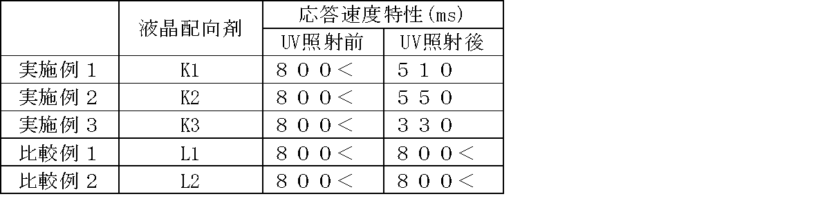
- the response speed characteristics of these liquid crystal cells were measured by the method described later. Thereafter, UV (wavelength: 280 to 330 nm) was irradiated by 20 J from the outside of the liquid crystal cell in a state where a voltage of 20 Vp-p was applied to the liquid crystal cell. Thereafter, the response speed characteristic was measured again, and the response speed before and after UV irradiation was compared. The results are shown in Table 1.
- Example 2 A liquid crystal cell was prepared in the same manner as in Example 1 except that the liquid crystal alignment treatment agent [K1] was changed to the liquid crystal alignment treatment agent [K2] obtained in Synthesis Example 2, and the response speed was measured. The results are shown in Table 1.
- Example 3 A liquid crystal cell was produced in the same manner as in Example 4 except that the liquid crystal alignment treatment agent [K1] was changed to the liquid crystal alignment treatment agent [K3] obtained in Synthesis Example 3, and the response speed was measured. The results are shown in Table 1.
- the response speed was improved after UV irradiation even when the liquid crystal to which no polymerizable compound was added was used.
- the response speed did not improve before and after UV irradiation.
- the liquid crystal aligning agent of the present invention can improve the response speed and obtain a good alignment state even in the case of a PSA system in which a polymerizable compound is added to the liquid crystal or a liquid crystal in which no polymerizable compound is added.
- the liquid crystal display element produced using the liquid crystal aligning agent of this invention is useful as a TFT liquid crystal display element, a TN liquid crystal display element, a VA liquid crystal display element, etc.
Landscapes
- Physics & Mathematics (AREA)
- Chemical & Material Sciences (AREA)
- Nonlinear Science (AREA)
- Spectroscopy & Molecular Physics (AREA)
- Crystallography & Structural Chemistry (AREA)
- Organic Chemistry (AREA)
- Mathematical Physics (AREA)
- General Physics & Mathematics (AREA)
- Optics & Photonics (AREA)
- Chemical Kinetics & Catalysis (AREA)
- Health & Medical Sciences (AREA)
- Medicinal Chemistry (AREA)
- Polymers & Plastics (AREA)
- Materials Engineering (AREA)
- Engineering & Computer Science (AREA)
- Liquid Crystal (AREA)
- Silicon Polymers (AREA)
Abstract
Description
また、テトラアルコキシシラン、特定のトリアルコキシシラン及び水との反応生成物、特定のグリコールエーテル系溶媒を含有する液晶配向剤組成物を使用することにより、表示不良を防止し、長時間駆動後も残像を残さず、液晶を配向させる能力を低下させることなく、且つ光及び熱に対する電圧保持率の低下が少ない液晶配向膜を形成することが報告されている。(特許文献3参照。)
[1]式(1)で表されるアルコキシシラン及び式(2)で表されるアルコキシシランを含むアルコキシシランを重縮合して得られるポリシロキサンを含有することを特徴とする素子用液晶配向剤。
R1Si(OR2)3 (1)
(R1はフッ素原子で置換されていてもよい、炭素原子数8~30の炭化水素基であり、R2は炭素原子数1~5のアルキル基を表す。)

[3]前記式(2)のR3が下記式(3)(ただし、m、nはそれぞれ0~6の整数である)で表される上記[1]に記載の液晶配向剤。

(R5)nSi(OR6)4-n (4)
(R5は、水素原子、又はヘテロ原子、ハロゲン原子、アミノ基、グリシドキシ基、メルカプト基、イソシアネート基若しくはウレイド基で置換されていてもよい、炭素原子数1~6の炭化水素基であり、R6は炭素原子数1~5のアルキル基であり、nは0~3の整数を表す。)
[6]前記ポリシロキサンが、式(1)で表されるアルコキシシランを全アルコキシシラン中、0.1~30モル%含み、かつ前記式(2)で表されるアルコキシシランを全アルコキシシラン中、3~70モル%含むアルコキシシランを重縮合して得られる上記[1]~[5]のいずれかに記載の液晶配向剤。
[7]前記ポリシロキサンが、式(4)で表されるアルコキシシランを全アルコキシシラン中、10~96.9モル%含むアルコキシシランを重縮合して得られる上記[4]~[6]のいずれかに記載の液晶配向剤。
[9]上記[1]~[8]のいずれかに記載の液晶配向剤を基板に塗布し、乾燥、焼成して得られる液晶配向膜。
[10]上記[9]に記載の液晶配向膜を有する液晶表示素子。
[11]上記[1]~[8]のいずれかに記載の液晶配向剤を塗布し、焼成された2枚の基板で液晶が挟持された液晶セルに、電圧を印加した状態でUVを照射した液晶表示素子。
[12]上記[1]~[8]のいずれかに記載の液晶配向剤を塗布し、焼成した2枚の基板で液晶を挟持し、電圧を印加した状態でUVを照射する液晶表示素子の製造方法。
[ポリシロキサン]
本発明は、式(1)で表されるアルコキシシラン及び式(2)で表されるアルコキシシランを含むアルコキシシランを重縮合して得られるポリシロキサンを含有するPSA方式用液晶配向剤である。
R1Si(OR2)3 (1)
R1はフッ素原子で置換されていてもよい炭素原子数8~30の炭化水素基であり、R2は炭素原子数1~5のアルキル基を表す。なお、本明細書において「置換されていてもよい」とは、「置換された又は置換されていない」を意味する。

かかる式(1)で表されるアルコキシシランの具体例を挙げるが、これに限定されるものではない。

本発明では、式(1)で表されるアルコキシシランが、使用される全アルコキシシラン中、好ましくは0.1~30モル%、特に好ましくは2~20モル%含まれ、かつ式(2)で表されるアルコキシシランが使用される全アルコキシシラン中、3~70モル%、特に好ましくは5~30モル%含まれるのが好ましい。
(R5)nSi(OR6)4-n (4)
R5は、水素原子、又はヘテロ原子、ハロゲン原子、アミノ基、グリシドキシ基、メルカプト基、イソシアネート基若しくはウレイド基で置換されていてもよい、炭素原子数1~6の炭化水素基である。R6は炭素原子数1~5、好ましくは1~3のアルキル基であり、nは0~3、好ましくは0~2の整数を表す。
式(4)のアルコキシシランにおいて、R5が水素原子である場合のアルコキシシランの具体例としては、トリメトキシシラン、トリエトキシシラン、トリプロポキシシラン、トリブトキシシラン等が挙げられる。
式(4)で表されるアルコキシシランにおいて、nが0であるアルコキシシランは、テトラアルコキシシランである。テトラアルコキシシランは、式(1)及び式(2)で表されるアルコキシシランと縮合し易いので、本発明のポリシロキサンを得るために好ましい。
このような式(4)においてnが0であるアルコキシシランとしては、テトラメトキシシラン、テトラエトキシシラン、テトラプロポキシシラン又はテトラブトキシシランがより好ましく、特に、テトラメトキシシラン又はテトラエトキシシランが好ましい。
本発明に用いるポリシロキサンを得る方法は特に限定されない。本発明においては、上記した式(1)及び式(2)を必須成分とするアルコキシシランを有機溶媒中で縮合させて得られる。通常、ポリシロキサンは、このようなアルコキシシランを重縮合して、有機溶媒に均一に溶解した溶液として得られる。
ポリシロキサンを重縮合する方法として、例えば、アルコキシシランをアルコール又はグリコールなどの溶媒中で加水分解・縮合する方法が挙げられる。その際、加水分解・縮合反応は、部分加水分解及び完全加水分解のいずれであってもよい。完全加水分解の場合は、理論上、アルコキシシラン中の全アルコキシ基の0.5倍モルの水を加えればよいが、通常は0.5倍モルより過剰量の水を加えるのが好ましい。
本発明においては、上記反応に用いる水の量は、所望により適宜選択することができるが、通常、アルコキシシラン中の全アルコキシ基の0.5~2.5倍モルであるのが好ましい。
アルコキシシランを重縮合する際に用いられる溶媒(以下、重合溶媒ともいう)は、アルコキシシランを溶解するものであれば特に限定されない。また、アルコキシシランが溶解しない場合でも、アルコキシシランの重縮合反応の進行とともに溶解するものであればよい。一般的には、アルコキシシランの重縮合反応によりアルコールが生成するため、アルコール類、グリコール類、グリコールエーテル類、又はアルコール類と相溶性の良好な有機溶媒が用いられる。
上記の方法で得られたポリシロキサンの重合溶液(以下、重合溶液ともいう。)は、原料として仕込んだ全アルコキシシランの有するケイ素原子をSiO2に換算した濃度(以下、SiO2換算濃度と称す。)が好ましくは20質量%以下、さらには5~15質量%とすることがより好ましい。この濃度範囲において任意の濃度を選択することにより、ゲルの生成を抑え、均質な溶液を得ることができる。
本発明においては、上記の方法で得られた重合溶液をそのままポリシロキサンの溶液としてもよいし、必要に応じて、上記の方法で得られた溶液を、濃縮したり、溶媒を加えて希釈したり又は他の溶媒に置換して、ポリシロキサンの溶液としてもよい。
その際、用いる溶媒(以下、添加溶媒ともいう)は、重合溶媒と同じでもよいし、別の溶媒でもよい。この添加溶媒は、ポリシロキサンが均一に溶解している限りにおいて特に限定されず、一種でも複数種でも任意に選択して用いることができる。
これらの溶媒は、液晶配向剤の粘度の調整、又はスピンコート、フレキソ印刷、インクジェット等で液晶配向剤を基板上に塗布する際の塗布性を向上できる。
本発明においては、本発明の効果を損なわない限りにおいて、ポリシロキサン以外のその他の成分、例えば、無機微粒子、メタロキサンオリゴマー、メタロキサンポリマー、レベリング剤、更に界面活性剤等の成分が含まれていてもよい。
無機微粒子としては、シリカ微粒子、アルミナ微粒子、チタニア微粒子、又はフッ化マグネシウム微粒子等の微粒子が好ましく、特にコロイド溶液の状態であるものが好ましい。このコロイド溶液は、無機微粒子を分散媒に分散したものでもよいし、市販品のコロイド溶液であってもよい。本発明においては、無機微粒子を含有させることにより、形成される硬化被膜の表面形状を変更したり、その他の機能を付与することが可能となる。無機微粒子としては、その平均粒子径が0.001~0.2μmであることが好ましく、更に好ましくは0.001~0.1μmである。無機微粒子の平均粒子径が0.2μmを超える場合には、調製される塗布液を用いて形成される硬化被膜の透明性が低下する場合がある。
無機微粒子の分散媒としては、水及び有機溶剤を挙げることができる。コロイド溶液としては、被膜形成用塗布液の安定性の観点から、pH又はpKaが1~10に調整されていることが好ましい。より好ましくは2~7である。
市販品のメタロキサンオリゴマー、メタロキサンポリマーの具体例としては、コルコート社製の、メチルシリケート51、メチルシリケート53A、エチルシリケート40、エチルシリケート48、EMS-485、SS-101等のシロキサンオリゴマー又はシロキサンポリマー、関東化学社製のチタニウム-n-ブトキシドテトラマー等のチタノキサンオリゴマーが挙げられる。これらは単独又は2種以上混合して使用してもよい。
また、ポリシロキサンに、上記したその他の成分を混合する方法は、ポリシロキサンと同時でも、後であってもよく、特に限定されない。
本発明の液晶配向剤は、上述したポリシロキサン、必要に応じてその他の成分を含有する溶液である。その際、溶媒としては、上述したポリシロキサンの重合溶媒および添加溶媒からなる群から選ばれる溶媒が用いられる。液晶配向剤におけるポリシロキサンの含有量は、SiO2換算濃度が好ましくは0.5~15質量%、より好ましくは1~6質量%である。このようなSiO2換算濃度の範囲であれば、一回の塗布で所望の膜厚を得やすく、充分な溶液のポットライフが得られ易い。
また、液晶配向剤中におけるポリシロキサンの含有量を調整する際には、上述したポリシロキサンの重合溶媒及び添加溶媒からなる群から選ばれる溶媒を用いることができる。
本発明の液晶配向膜は、本発明の液晶配向剤を用いて得られる。例えば、本発明の液晶配向剤を、基板に塗布した後、乾燥・焼成を行うことで得られる硬化膜を、そのまま液晶配向膜として用いることもできる。また、この硬化膜をラビングしたり、偏光又は特定の波長の光等を照射したり、イオンビーム等の処理をしたり、液晶充填後の液晶表示素子に電圧を印加した状態でUVを照射することも可能である。本発明の液晶配向剤は、液晶に重合性化合物が添加されるPSA方式の場合でも、液晶に重合性化合物が添加されない場合でも有用である。
液晶配向剤を塗布する基板としては、透明性の高い基板であれば特に限定されないが、基板上に液晶を駆動するための透明電極が形成された基板が好ましい。
液晶配向剤の塗布方法としては、スピンコート法、印刷法、インクジェット法、スプレー法、ロールコート法などが挙げられるが、生産性の面から工業的には転写印刷法が広く用いられており、本発明でも好適に用いられる。
上記の方法で液晶配向剤を塗布して形成される塗膜は、焼成して硬化膜とすることができる。その際、焼成温度は、100℃~350℃の任意の温度で行うことができるが、好ましくは140℃~300℃であり、より好ましくは150℃~230℃、更に好ましくは160℃~220℃である。焼成時間は5分~240分の任意の時間で焼成を行うことができる。好ましくは10~90分であり、より好ましくは20~90分である。加熱は、通常公知の方法、例えば、ホットプレート、熱風循環オーブン、IR(赤外線)オーブン、ベルト炉などを用いることができる。
この硬化膜の厚みは必要に応じて選択することができるが、好ましくは5nm以上、より好ましくは10nm以上の場合、液晶表示素子の信頼性が得られ易いので好適である。また、硬化膜の厚みが好ましくは300nm以下、より好ましくは150nm以下の場合は、液晶表示素子の消費電力が極端に大きくならないので好適である。
本発明の液晶表示素子は、上記の方法により、基板に液晶配向膜を形成した後、公知の方法で液晶セルを作製して得ることができる。液晶セル作製の一例を挙げると、液晶配向膜が形成された1対の基板を、スペーサーを挟んで、シール剤で固定し、液晶を注入して封止する方法が一般的である。その際、用いるスペーサーの大きさは1~30μmであるが、好ましくは2~10μmである。
液晶を注入する方法は特に制限されず、作製した液晶セル内を減圧にした後、液晶を注入する真空法、液晶を滴下した後に封止を行う滴下法などを挙げることができる。
透過型の液晶素子の場合は、上記の如き基板を用いることが一般的であるが、反射型の液晶表示素子では、片側の基板のみにならばシリコンウエハー等の不透明な基板も用いることが可能である。その際、基板に形成された電極には、光を反射するアルミニウムの如き材料を用いることもできる。
本実施例で用いた化合物における略語は以下のとおりである。
TEOS:テトラエトキシシラン
C18:オクタデシルトリエトキシシラン
VTES:ビニルトリエトキシシラン
ARMS:アリルトリメトキシシラン
OTMS:オクテニルトリメトキシシラン
STMS:スチリルトリメトキシシラン
HG:2-メチル-2,4-ペンタンジオール(別名:ヘキシレングリコール)
BCS:2-ブトキシエタノール
UPS:3-ウレイドプロピルエトキシシラン
温度計、還流管を備え付けた200mLの四つ口反応フラスコ中でHG24.0g、BCS8.0g、TEOS27.9g、C18を1.7g、及びARMSを9.7g混合して、アルコキシシランモノマーの溶液を調製した。この溶液に、予めHG12.0g、BCS4.0g、水10.8g及び触媒として蓚酸0.9gを混合した溶液を、室温下で30分かけて滴下した。この溶液を30分間撹拌してから1時間還流させた後、予めUPS含有量92質量%のメタノール溶液0.6g、HG0.3g及びBCS0.1gの混合液を加えた。更に30分間還流させてから放冷してSiO2換算濃度が12重量%のポリシロキサン溶液を得た。
得られたポリシロキサン溶液10.0gに対し、BCS20.0gを混合し、SiO2換算濃度が4重量%の液晶配向剤(K1)を得た。
温度計、還流管を備え付けた200mLの四つ口反応フラスコ中でHG21.6g、BCS7.2g、TEOS27.5g、C18を1.7g、及びOTMSを13.9g混合して、アルコキシシランモノマーの溶液を調製した。この溶液に、予めHG10.8g、BCS3.6g、水10.8g及び触媒として蓚酸0.9gを混合した溶液を、室温下で30分かけて滴下した。この溶液を30分間撹拌してから1時間還流させた後、予めUPS含有量92質量%のメタノール溶液1.2g、HG0.6g及びBCS0.2gの混合液を加えた。更に30分間還流させてから放冷してSiO2換算濃度が12重量%のポリシロキサン溶液を得た。
得られたポリシロキサン溶液10.0gに対し、BCS20.0gを混合し、SiO2換算濃度が4重量%の液晶配向剤(K2)を得た。
温度計、還流管を備え付けた200mLの四つ口反応フラスコ中でHG21.8g、BCS7.3g、TEOS27.5g、C18を1.7g、及びSTMSを13.5g混合して、アルコキシシランモノマーの溶液を調製した。この溶液に、予めHG10.9g、BCS3.6g、水10.8g及び触媒として蓚酸0.9gを混合した溶液を、室温下で30分かけて滴下した。この溶液を30分間撹拌してから1時間還流させた後、予めUPS含有量92質量%のメタノール溶液1.2g、HG0.6g及びBCS0.2gの混合液を加えた。更に30分間還流させてから放冷してSiO2換算濃度が12重量%のポリシロキサン溶液を得た。
得られたポリシロキサン溶液10.0gに対し、BCS20.0gを混合し、SiO2換算濃度が4重量%の液晶配向剤(K3)を得た。
温度計、還流管を備え付けた200mLの四つ口反応フラスコ中でHG23.3g、BCS7.7g、TEOS40.8g、C18を1.7g混合して、アルコキシシランモノマーの溶液を調製した。この溶液に、予めHG11.6g、BCS3.9g、水10.8g及び触媒として蓚酸0.2gを混合した溶液を、室温下で30分かけて滴下した。この溶液を30分間撹拌してから1時間還流させた後に放冷してSiO2換算固形分濃度が12重量%のポリシロキサン溶液を得た。
得られたポリシロキサン溶液10.0gに対し、BCS20.0gを混合し、SiO2換算濃度が4重量%の液晶配向剤(L1)を得た。
温度計、還流管を備え付けた200mLの四つ口反応フラスコ中でHG21.8g、BCS7.3g、TEOS27.5g、C18を1.7g及びVTESを13.5g混合して、アルコキシシランモノマーの溶液を調製した。この溶液に、予めHG10.9g、BCS3.6g、水10.8g及び触媒として蓚酸0.9gを混合した溶液を、室温下で30分かけて滴下した。この溶液を30分間撹拌してから1時間還流させた後、予めUPS含有量92質量%のメタノール溶液1.2g、HG0.6g及びBCS0.2gの混合液を加えた。更に30分間還流させてから放冷してSiO2換算濃度が12重量%のポリシロキサン溶液を得た。
得られたポリシロキサン溶液10.0gに対し、BCS20.0gを混合し、SiO2換算濃度が4重量%の液晶配向剤(L2)を得た。
合成例1で得られた液晶配向処理剤[K1]を、画素サイズが100μm×300μmで、ライン/スペースがそれぞれ5μmのITO電極パターンが形成されているITO電極基板のITO面にスピンコートした。80℃のホットプレートで5分間乾燥した後、180℃の熱風循環式オーブンで30分間焼成を行い、膜厚100nmの液晶配向膜を形成した。
合成例1で得られた液晶配向処理剤[K1]を、電極パターンが形成されていないITO面にスピンコートし、80℃のホットプレートで5分間乾燥した後、180℃の熱風循環式オーブンで30分間焼成を行い、膜厚100nmの液晶配向膜を形成した。これらの2枚の基板を用意し、一方の基板の液晶配向膜面上に6μmのビーズスペーサーを散布した後、その上からシール剤を印刷した。他方の基板を液晶配向膜面を内側にし、張り合わせた後、シール剤を硬化させて空セルを作製した。液晶MLC-6608(メルク社製商品名)を、空セルに減圧注入法によって、前記液晶を注入した液晶セルを作製した。
液晶配向処理剤[K1]を合成例2で得られた液晶配向処理剤[K2]に変更した以外は、実施例1と同様にして液晶セルを作製し、応答速度を測定した。その結果を表1に示した。
液晶配向処理剤[K1]を合成例3で得られた液晶配向処理剤[K3]に変更した以外は、実施例4と同様にして液晶セルを作製し、応答速度を測定した。その結果を表1に示した。
液晶配向処理剤[K1]を比較合成例1で得られた液晶配向処理剤[L1]に変更した以外は、実施例1~実施例3と同様にして液晶セルを作製し、応答速度を測定した。その結果を表1に示した。
液晶配向処理剤[K1]を比較合成例2で得られた液晶配向処理剤[L2]に変更した以外は、実施例1~実施例3と同様にして液晶セルを作製し、応答速度を測定した。その結果を表1に示した。
電圧を印加していない液晶セルに、電圧 ±4V、周波数1kHzの矩形波を印加した際の、液晶パネルの輝度の時間変化をオシロスコープにて取り込んだ。電圧を印加していない時の輝度を0%、±4Vの電圧を印加し、飽和した輝度の値を100%として、輝度が10%~90%まで変化する時間を立ち上がりの応答速度(単位:ミリセコンド)とした。
Claims (12)
- 式(1)で表されるアルコキシシラン及び式(2)で表されるアルコキシシランを含むアルコキシシランを重縮合して得られるポリシロキサンを含有することを特徴とする液晶配向剤。
R1Si(OR2)3 (1)
(R1はフッ素原子で置換されていてもよい、炭素原子数8~30の炭化水素基であり、R2は炭素原子数1~5のアルキル基を表す。)

- 前記式(2)のR3がアルキレン基である請求項1に記載の液晶配向剤。
- 前記式(2)のR3が下記式(3)(ただし、m、nはそれぞれ0~6の整数である)で表される請求項1に記載の液晶配向剤。

- ポリシロキサンが、さらに、下記式(4)で表されるアルコキシシランを含有するアルコキシシランを重縮合して得られるポリシロキサンである、請求項1~3のいずれかに記載の液晶配向剤。
(R5)nSi(OR6)4-n (4)
(R5は、水素原子、又はヘテロ原子、ハロゲン原子、アミノ基、グリシドキシ基、メルカプト基、イソシアネート基若しくはウレイド基で置換されていてもよい、炭素原子数1~6の炭化水素基であり、R6は炭素原子数1~5のアルキル基であり、nは0~3の整数を表す。) - 前記式(4)で表されるアルコキシシランが、式(4)におけるnが0である、テトラアルコキシシランである請求項4に記載の液晶配向剤。
- 前記ポリシロキサンが、式(1)で表されるアルコキシシランを全アルコキシシラン中、0.1~30モル%含み、かつ前記式(2)で表されるアルコキシシランを全アルコキシシラン中、3~70モル%含むアルコキシシランを重縮合して得られる請求項1~5のいずれかに記載の液晶配向剤。
- 前記ポリシロキサンが、式(4)で表されるアルコキシシランを全アルコキシシラン中、10~96.9モル%含むアルコキシシランを重縮合して得られる請求項4~6のいずれかに記載の液晶配向剤。
- ポリシロキサンの含有量が、SiO2換算濃度で、0.5~15質量%含有される請求項1~6のいずれかに記載の液晶配向剤。
- 請求項1~8のいずれかに記載の液晶配向剤を基板に塗布し、乾燥、焼成して得られる液晶配向膜。
- 請求項9に記載の液晶配向膜を有する液晶表示素子。
- 請求項1~8のいずれかに記載の液晶配向剤を塗布し、焼成された2枚の基板で液晶が挟持された液晶セルに、電圧を印加した状態でUVを照射した液晶表示素子。
- 請求項1~8のいずれかに記載の液晶配向剤を塗布し、焼成した2枚の基板で液晶を挟持し、電圧を印加した状態でUVを照射する液晶表示素子の製造方法。
Priority Applications (3)
| Application Number | Priority Date | Filing Date | Title |
|---|---|---|---|
| KR1020127028406A KR101829479B1 (ko) | 2010-04-06 | 2011-04-04 | 액정 배향제, 액정 배향막 및 액정 표시 소자 |
| JP2012509656A JP5761180B2 (ja) | 2010-04-06 | 2011-04-04 | 液晶配向剤、液晶配向膜及び液晶表示素子 |
| CN201180027621.3A CN102934013B (zh) | 2010-04-06 | 2011-04-04 | 液晶取向剂、液晶取向膜及液晶显示元件 |
Applications Claiming Priority (2)
| Application Number | Priority Date | Filing Date | Title |
|---|---|---|---|
| JP2010088014 | 2010-04-06 | ||
| JP2010-088014 | 2010-04-06 |
Publications (1)
| Publication Number | Publication Date |
|---|---|
| WO2011125984A1 true WO2011125984A1 (ja) | 2011-10-13 |
Family
ID=44762919
Family Applications (1)
| Application Number | Title | Priority Date | Filing Date |
|---|---|---|---|
| PCT/JP2011/058553 Ceased WO2011125984A1 (ja) | 2010-04-06 | 2011-04-04 | 液晶配向剤、液晶配向膜及び液晶表示素子 |
Country Status (5)
| Country | Link |
|---|---|
| JP (1) | JP5761180B2 (ja) |
| KR (1) | KR101829479B1 (ja) |
| CN (1) | CN102934013B (ja) |
| TW (1) | TWI515234B (ja) |
| WO (1) | WO2011125984A1 (ja) |
Cited By (4)
| Publication number | Priority date | Publication date | Assignee | Title |
|---|---|---|---|---|
| KR20140106392A (ko) * | 2013-02-25 | 2014-09-03 | 제이에스알 가부시끼가이샤 | 액정 표시 소자용 조성물, 액정 배향막, 그리고 액정 표시 소자 및 그의 제조 방법 |
| CN104903786A (zh) * | 2012-11-06 | 2015-09-09 | 日产化学工业株式会社 | 液晶取向剂、液晶取向膜及液晶显示元件 |
| JP2016216589A (ja) * | 2015-05-19 | 2016-12-22 | Dic株式会社 | ポリシロキサン、樹脂組成物、塗料及び積層体 |
| WO2025041708A1 (ja) * | 2023-08-21 | 2025-02-27 | 日産化学株式会社 | 反射防止膜付き基板の製造方法、及び反射防止膜付き基板 |
Families Citing this family (2)
| Publication number | Priority date | Publication date | Assignee | Title |
|---|---|---|---|---|
| KR102344233B1 (ko) * | 2013-06-06 | 2021-12-27 | 닛산 가가쿠 가부시키가이샤 | 액정 배향제, 액정 배향막 및 액정 표시 소자 |
| CN110109293A (zh) * | 2019-04-04 | 2019-08-09 | 深圳市华星光电技术有限公司 | 液晶无机配向薄膜的制造方法 |
Citations (5)
| Publication number | Priority date | Publication date | Assignee | Title |
|---|---|---|---|---|
| JPH04356020A (ja) * | 1990-09-17 | 1992-12-09 | Matsushita Electric Ind Co Ltd | 液晶配向膜及びその製造方法並びに液晶表示装置及びその製造方法 |
| JPH10153783A (ja) * | 1996-07-30 | 1998-06-09 | Matsushita Electric Ind Co Ltd | 液晶配向膜とその製造方法およびそれを用いた液晶表示装置とその製造方法 |
| JP2002214617A (ja) * | 2000-11-14 | 2002-07-31 | Matsushita Electric Ind Co Ltd | 化学吸着液及びこれを用いた化学吸着膜の製造方法 |
| JP2007025530A (ja) * | 2005-07-21 | 2007-02-01 | Seiko Epson Corp | 液晶装置及びその製造方法、並びに電子機器 |
| WO2009148099A1 (ja) * | 2008-06-04 | 2009-12-10 | 日産化学工業株式会社 | ケイ素系液晶配向剤、液晶配向膜及び液晶表示素子 |
Family Cites Families (5)
| Publication number | Priority date | Publication date | Assignee | Title |
|---|---|---|---|---|
| DE59707681D1 (de) * | 1996-10-28 | 2002-08-14 | Rolic Ag Zug | Vernetzbare, photoaktive Silanderivate |
| DE59807348D1 (de) * | 1997-02-05 | 2003-04-10 | Rolic Ag Zug | Photovernetzbare Silanderivate |
| JP4702198B2 (ja) | 2006-06-27 | 2011-06-15 | セイコーエプソン株式会社 | 配向膜、配向膜の形成方法、電子デバイス用基板、液晶パネルおよび電子機器 |
| KR101157338B1 (ko) * | 2007-08-21 | 2012-06-18 | 제이에스알 가부시끼가이샤 | 액정 배향제, 액정 배향막의 제조 방법 및 액정 표시 소자 |
| JP4985609B2 (ja) * | 2007-12-26 | 2012-07-25 | Jnc株式会社 | 液晶配向剤、液晶配向膜及び液晶表示素子 |
-
2011
- 2011-04-04 JP JP2012509656A patent/JP5761180B2/ja active Active
- 2011-04-04 KR KR1020127028406A patent/KR101829479B1/ko active Active
- 2011-04-04 WO PCT/JP2011/058553 patent/WO2011125984A1/ja not_active Ceased
- 2011-04-04 CN CN201180027621.3A patent/CN102934013B/zh active Active
- 2011-04-06 TW TW100111796A patent/TWI515234B/zh active
Patent Citations (5)
| Publication number | Priority date | Publication date | Assignee | Title |
|---|---|---|---|---|
| JPH04356020A (ja) * | 1990-09-17 | 1992-12-09 | Matsushita Electric Ind Co Ltd | 液晶配向膜及びその製造方法並びに液晶表示装置及びその製造方法 |
| JPH10153783A (ja) * | 1996-07-30 | 1998-06-09 | Matsushita Electric Ind Co Ltd | 液晶配向膜とその製造方法およびそれを用いた液晶表示装置とその製造方法 |
| JP2002214617A (ja) * | 2000-11-14 | 2002-07-31 | Matsushita Electric Ind Co Ltd | 化学吸着液及びこれを用いた化学吸着膜の製造方法 |
| JP2007025530A (ja) * | 2005-07-21 | 2007-02-01 | Seiko Epson Corp | 液晶装置及びその製造方法、並びに電子機器 |
| WO2009148099A1 (ja) * | 2008-06-04 | 2009-12-10 | 日産化学工業株式会社 | ケイ素系液晶配向剤、液晶配向膜及び液晶表示素子 |
Cited By (7)
| Publication number | Priority date | Publication date | Assignee | Title |
|---|---|---|---|---|
| CN104903786A (zh) * | 2012-11-06 | 2015-09-09 | 日产化学工业株式会社 | 液晶取向剂、液晶取向膜及液晶显示元件 |
| CN104903786B (zh) * | 2012-11-06 | 2017-12-08 | 日产化学工业株式会社 | 液晶取向剂、液晶取向膜及液晶显示元件 |
| KR20140106392A (ko) * | 2013-02-25 | 2014-09-03 | 제이에스알 가부시끼가이샤 | 액정 표시 소자용 조성물, 액정 배향막, 그리고 액정 표시 소자 및 그의 제조 방법 |
| JP2014186301A (ja) * | 2013-02-25 | 2014-10-02 | Jsr Corp | 液晶表示素子用組成物、並びに液晶表示素子及びその製造方法 |
| KR102129496B1 (ko) * | 2013-02-25 | 2020-07-02 | 제이에스알 가부시끼가이샤 | 액정 표시 소자용 조성물, 액정 배향막, 그리고 액정 표시 소자 및 그의 제조 방법 |
| JP2016216589A (ja) * | 2015-05-19 | 2016-12-22 | Dic株式会社 | ポリシロキサン、樹脂組成物、塗料及び積層体 |
| WO2025041708A1 (ja) * | 2023-08-21 | 2025-02-27 | 日産化学株式会社 | 反射防止膜付き基板の製造方法、及び反射防止膜付き基板 |
Also Published As
| Publication number | Publication date |
|---|---|
| KR101829479B1 (ko) | 2018-02-14 |
| TW201231506A (en) | 2012-08-01 |
| JPWO2011125984A1 (ja) | 2013-07-11 |
| CN102934013B (zh) | 2016-03-16 |
| KR20130040847A (ko) | 2013-04-24 |
| JP5761180B2 (ja) | 2015-08-12 |
| TWI515234B (zh) | 2016-01-01 |
| CN102934013A (zh) | 2013-02-13 |
Similar Documents
| Publication | Publication Date | Title |
|---|---|---|
| JP5605359B2 (ja) | ケイ素系液晶配向剤、液晶配向膜及び液晶表示素子 | |
| JP5578074B2 (ja) | ケイ素系液晶配向剤、液晶配向膜及び液晶表示素子 | |
| JP5206413B2 (ja) | ケイ素系液晶配向剤及び液晶配向膜 | |
| JP5459229B2 (ja) | インクジェット塗布用液晶配向剤、液晶配向膜及び液晶表示素子 | |
| JP5593611B2 (ja) | 珪素系液晶配向剤、液晶配向膜並びにそれらの製造方法 | |
| JP6079626B2 (ja) | ケイ素系液晶配向剤、液晶配向膜及び液晶表示素子 | |
| JP5761180B2 (ja) | 液晶配向剤、液晶配向膜及び液晶表示素子 | |
| WO2010074261A1 (ja) | インクジェット塗布用液晶配向剤、液晶配向膜及び液晶表示素子 | |
| JP5716673B2 (ja) | ケイ素系液晶配向剤、液晶配向膜及び液晶表示素子 | |
| JP6107661B2 (ja) | ケイ素系液晶配向剤、液晶配向膜及び液晶表示素子 | |
| JP5999084B2 (ja) | ケイ素系液晶配向剤、液晶配向膜及び液晶表示素子 | |
| WO2014021174A1 (ja) | 液晶配向剤、液晶配向膜、液晶表示素子及び液晶表示素子の製造方法 | |
| JPWO2010074261A1 (ja) | インクジェット塗布用液晶配向剤、液晶配向膜及び液晶表示素子 |
Legal Events
| Date | Code | Title | Description |
|---|---|---|---|
| WWE | Wipo information: entry into national phase |
Ref document number: 201180027621.3 Country of ref document: CN |
|
| 121 | Ep: the epo has been informed by wipo that ep was designated in this application |
Ref document number: 11765884 Country of ref document: EP Kind code of ref document: A1 |
|
| WWE | Wipo information: entry into national phase |
Ref document number: 2012509656 Country of ref document: JP |
|
| NENP | Non-entry into the national phase |
Ref country code: DE |
|
| ENP | Entry into the national phase |
Ref document number: 20127028406 Country of ref document: KR Kind code of ref document: A |
|
| 122 | Ep: pct application non-entry in european phase |
Ref document number: 11765884 Country of ref document: EP Kind code of ref document: A1 |