WO2011125841A1 - フェイズロックドループ回路 - Google Patents
フェイズロックドループ回路 Download PDFInfo
- Publication number
- WO2011125841A1 WO2011125841A1 PCT/JP2011/058224 JP2011058224W WO2011125841A1 WO 2011125841 A1 WO2011125841 A1 WO 2011125841A1 JP 2011058224 W JP2011058224 W JP 2011058224W WO 2011125841 A1 WO2011125841 A1 WO 2011125841A1
- Authority
- WO
- WIPO (PCT)
- Prior art keywords
- phase
- signal
- locked loop
- loop circuit
- voltage
- Prior art date
- Legal status (The legal status is an assumption and is not a legal conclusion. Google has not performed a legal analysis and makes no representation as to the accuracy of the status listed.)
- Ceased
Links
Images



Classifications
-
- G—PHYSICS
- G09—EDUCATION; CRYPTOGRAPHY; DISPLAY; ADVERTISING; SEALS
- G09G—ARRANGEMENTS OR CIRCUITS FOR CONTROL OF INDICATING DEVICES USING STATIC MEANS TO PRESENT VARIABLE INFORMATION
- G09G3/00—Control arrangements or circuits, of interest only in connection with visual indicators other than cathode-ray tubes
- G09G3/20—Control arrangements or circuits, of interest only in connection with visual indicators other than cathode-ray tubes for presentation of an assembly of a number of characters, e.g. a page, by composing the assembly by combination of individual elements arranged in a matrix no fixed position being assigned to or needed to be assigned to the individual characters or partial characters
- G09G3/2092—Details of a display terminals using a flat panel, the details relating to the control arrangement of the display terminal and to the interfaces thereto
- G09G3/2096—Details of the interface to the display terminal specific for a flat panel
-
- G—PHYSICS
- G09—EDUCATION; CRYPTOGRAPHY; DISPLAY; ADVERTISING; SEALS
- G09G—ARRANGEMENTS OR CIRCUITS FOR CONTROL OF INDICATING DEVICES USING STATIC MEANS TO PRESENT VARIABLE INFORMATION
- G09G5/00—Control arrangements or circuits for visual indicators common to cathode-ray tube indicators and other visual indicators
- G09G5/003—Details of a display terminal, the details relating to the control arrangement of the display terminal and to the interfaces thereto
- G09G5/006—Details of the interface to the display terminal
- G09G5/008—Clock recovery
-
- H—ELECTRICITY
- H03—ELECTRONIC CIRCUITRY
- H03L—AUTOMATIC CONTROL, STARTING, SYNCHRONISATION OR STABILISATION OF GENERATORS OF ELECTRONIC OSCILLATIONS OR PULSES
- H03L7/00—Automatic control of frequency or phase; Synchronisation
- H03L7/06—Automatic control of frequency or phase; Synchronisation using a reference signal applied to a frequency- or phase-locked loop
- H03L7/08—Details of the phase-locked loop
- H03L7/085—Details of the phase-locked loop concerning mainly the frequency- or phase-detection arrangement including the filtering or amplification of its output signal
- H03L7/095—Details of the phase-locked loop concerning mainly the frequency- or phase-detection arrangement including the filtering or amplification of its output signal using a lock detector
Definitions
- the present invention relates to a phase-locked loop circuit that outputs a clock signal synchronized with an input signal such as a synchronization signal.
- liquid crystal display devices have been widely used in liquid crystal televisions, monitors, mobile phones and the like as flat panel displays having features such as thinness and light weight compared to conventional cathode ray tubes.
- a liquid crystal display device includes an illumination device (backlight) that emits light and a liquid crystal panel that displays a desired image by serving as a shutter for light from a light source provided in the illumination device. It is.
- the display operation is synchronized with a synchronization signal included in a video signal input from the outside. That is, the liquid crystal display device is provided with, for example, a phase-locked loop circuit described in Patent Document 1 below, and the display operation is synchronized with the synchronization signal by using the phase-locked loop circuit. .
- FIG. 7 is a circuit diagram showing a conventional phase-locked loop circuit.
- a conventional phase-locked loop circuit 51 includes a phase comparator 52, a DC bias 53, a low-pass filter 54, a voltage-controlled oscillator 55, and a frequency divider that are sequentially connected to the phase comparator 52. 56 are provided.
- the frequency divider 56 is connected to the phase comparator 52.
- the circuit configuration is configured in a loop.
- the phase comparator 52 is supplied with an external synchronization signal (syn) and a phase comparison signal (BLK) from the frequency divider 56.
- the phase comparator 52 compares the phases of the synchronization signal (syn) and the phase comparison signal (BLK), and outputs a phase comparison result signal indicating the phase comparison result.
- the DC bias 53 supplies a constant bias voltage (DC voltage) to the phase comparison result signal from the phase comparator 52 and outputs it as a first control voltage signal.
- the low-pass filter 54 smoothes the AC wave component included in the first control voltage signal from the DC bias 53 and outputs it as a second control voltage signal.
- the voltage control oscillator 55 oscillates a clock signal (ck) having a frequency corresponding to the voltage of the second control voltage signal from the low pass filter 54.
- the frequency divider 56 divides the clock signal (ck) from the voltage controlled oscillator 55 and outputs the divided clock signal to the phase comparator 52 as a phase comparison signal (BLK).
- a clock signal synchronized with the synchronization signal (syn) is output from the voltage controlled oscillator 55 or the frequency divider 56 to a control unit (not shown) provided in the liquid crystal display device. Thereby, in the liquid crystal display device, the display operation is performed in synchronization with the synchronization signal (syn).
- phase-locked loop circuit 51 it is expected that the response of the phase-locked loop circuit 51 is improved by increasing the gain of the low-pass filter 54.
- the phase-locked loop circuit 51 is likely to be affected by noise or the like, which may cause another problem that a malfunction may occur.
- an object of the present invention is to provide a phase-locked loop circuit capable of improving responsiveness.
- the phase-locked loop circuit compares the phase of an external input signal and a phase comparison signal, and outputs a phase comparison result signal indicating the phase comparison result.
- a comparator a bias unit for supplying a bias voltage to the phase comparison result signal from the phase comparator and outputting it as a first control voltage signal, and an alternating current included in the first control voltage signal from the bias unit
- a low-pass filter that smoothes a wave component and outputs it as a second control voltage signal, a voltage-controlled oscillator that oscillates a clock signal having a frequency corresponding to the voltage of the second control voltage signal from the low-pass filter, and the voltage control
- a phase-locked loop having a frequency divider that divides a clock signal from an oscillator and outputs the divided clock signal to the phase comparator as a phase comparison signal A road,
- a phase comparison result signal from the phase comparator is input, and based on the input phase comparison result signal, a lock state determination unit that determines a lock state in
- the lock state determination unit determines the lock state in the phase locked loop circuit based on the phase comparison result signal from the phase comparator. Further, the bias voltage creation unit creates a bias voltage in the bias unit based on the determination result of the lock state determination unit, and supplies the bias voltage to the bias unit. As a result, the locked state in the phase-locked loop circuit can be determined, and the optimum bias voltage corresponding to the determined locked state can be supplied to the phase comparison result signal. As a result, it is possible to accelerate the pull-in of synchronization in the phase-locked loop circuit, and it is possible to configure a phase-locked loop circuit that can improve responsiveness.
- a three-state buffer is used as the phase comparator, and when the three-state buffer is in an active state, the phase comparison signal from the frequency divider is used as the phase comparison result signal.
- the bias voltage generating unit generates a bias voltage in the bias unit based on a count value from the up / down counter.
- the locked state in the phase-locked loop circuit can be easily determined and can be easily changed with the optimum bias voltage.
- the clock signal from the voltage controlled oscillator or the clock signal from the voltage controlled oscillator is frequency-divided by the frequency divider as the predetermined clock signal.
- a signal is preferably used.
- phase-locked loop circuit with a simple structure can be configured.
- phase-locked loop circuit it is preferable that a self-running counter that is self-reset with a specific count value is used as the frequency divider.
- a phase-locked loop circuit having a simple structure can be configured as compared with the case where the frequency dividing operation by the frequency divider is controlled by external control.
- FIG. 1 is a circuit diagram showing a phase-locked loop circuit according to an embodiment of the present invention.
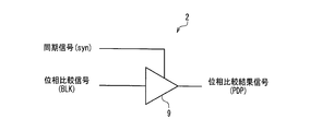
- FIG. 2 is a diagram illustrating a specific configuration of the phase comparator shown in FIG.
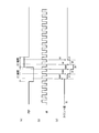
- FIG. 3 is a waveform diagram showing signal waveforms at various parts in the locked state in the phase-locked loop circuit.
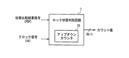
- FIG. 4 is a diagram for explaining a specific configuration of the lock state determination circuit shown in FIG.
- FIG. 5 is a diagram for explaining an operation example of the lock state determination circuit shown in FIG.
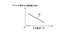
- FIG. 6 is a graph showing a specific example of voltage-frequency characteristics in the voltage controlled oscillator shown in FIG.
- FIG. 7 is a circuit diagram showing a conventional phase-locked loop circuit.
- phase-locked loop circuit of the present invention is provided in the liquid crystal display device and the display operation is synchronized with a synchronization signal will be described as an example.
- the dimension of the structural member in each figure does not faithfully represent the actual dimension of the structural member, the dimensional ratio of each structural member, or the like.
- FIG. 1 is a circuit diagram showing a phase-locked loop circuit according to an embodiment of the present invention.
- FIG. 2 is a diagram illustrating a specific configuration of the phase comparator shown in FIG.
- FIG. 3 is a waveform diagram showing signal waveforms at various parts in the locked state in the phase-locked loop circuit.
- FIG. 4 is a diagram for explaining a specific configuration of the lock state determination circuit shown in FIG.
- the phase-locked loop circuit 1 includes a phase comparator 2, a DC bias 3, a low-pass filter 4, a voltage controlled oscillator 5, and a split circuit sequentially connected to the phase comparator 2.
- a frequency divider 6 is provided, and the frequency divider 6 is connected to the phase comparator 2.
- the phase-locked loop circuit 1 includes a lock state determination circuit 7 as a lock state determination unit connected to the phase comparator 2 and the voltage controlled oscillator 5, and a bias connected to the lock state determination circuit 7 and the DC bias 3.
- a bias voltage generation circuit 8 as a voltage generation unit is provided, and the phase-locked loop circuit 1 is configured to change the bias voltage at the DC bias 3 based on the locked state (details will be described later). .)
- the phase comparator 2 receives a synchronization signal (syn) as an input signal from the outside and a phase comparison signal (BLK) from the frequency divider 6.
- the phase comparator 2 compares the phases of the synchronization signal (syn) and the phase comparison signal (BLK), and outputs the phase comparison result signal (PDP) indicating the phase comparison result to the DC bias 3 and the lock state determination circuit. 7 is output.
- a three-state buffer 9 is used in the phase comparator 2, and the three-state buffer 9 is in an active state (that is, a synchronization signal (for example, a positive signal) When the syn) is in the Hi period), the phase comparison signal (BLK) from the frequency divider 6 is output as the phase comparison result signal (PDP).
- a synchronization signal for example, a positive signal
- the Hi impedance output is used as a phase comparison result signal (PDP) when it is in an inactive state (that is, a state in which, for example, the synchronization signal (syn) including a positive signal is in the Lo period) It is designed to output.
- PDP phase comparison result signal
- the DC bias 3 constitutes a bias unit, and the bias voltage (DC voltage) created by the bias voltage creation circuit 8 is applied to the phase comparison result signal from the phase comparator 5. To supply and output as a first control voltage signal.
- the low-pass filter 4 smoothes the AC wave component included in the first control voltage signal from the DC bias 3 and outputs it to the voltage controlled oscillator 5 as the second control voltage signal.
- the voltage controlled oscillator 5 oscillates a clock signal (ck) having a frequency (specific frequency) corresponding to the voltage of the second control voltage signal from the low-pass filter 4.
- the frequency divider 6 is operated by a clock signal (ck) having a specific frequency from the voltage controlled oscillator 5. As a result, the frequency divider 6 divides the input clock signal (ck) and outputs it to the phase comparator 2 as a phase comparison signal (BLK).
- the frequency divider 6 is a self-running counter that is self-reset with a specific count value.
- phase locked loop circuit 1 the operations of the phase comparator 2, the DC bias 3, the low pass filter 4, the voltage controlled oscillator 5, and the frequency divider 6 are repeatedly performed, whereby the phase locked loop circuit 1. Becomes a stable state (that is, a locked state).
- a control signal synchronized with the synchronization signal (syn) is output from the voltage controlled oscillator 5 or the frequency divider 6 to a control unit (not shown) provided in the liquid crystal display device. Thereby, in the liquid crystal display device, the display operation is performed in synchronization with the synchronization signal (syn).
- the Hi period and the Lo period are almost equal. Therefore, when the phase-locked loop circuit 1 is locked, the phase comparison signal (BLK) from the frequency divider 6 is approximately at the center of the Hi period of the synchronization signal (syn) shown in FIG. It will stand up. Therefore, the lock state determination circuit 7 can determine the current lock state in the phase locked loop circuit 1 by comparing the time of the Hi period and the Lo period in the phase comparison signal (BLK).
- the lock state determination circuit 7 uses an up / down counter 10 that operates with a predetermined clock signal.
- the up / down counter 10 uses the clock signal (ck) from the voltage controlled oscillator 5 as the predetermined clock signal, and the phase comparison result signal from the three-state buffer 9 according to the clock signal (ck). It is configured to determine whether (PDP) is high level or low level and to increase or decrease the count value based on the determination result. More specifically, the up / down counter 10 counts up if the phase comparison result signal (PDP) is in the Hi period and counts down if the phase comparison result signal (PDP) is in the Lo period, for example, 6 bits. Is output to the bias voltage generation circuit 8.
- a D / A converter is used for the bias voltage generation circuit 8, and the count value from the up / down counter 10 is input, and an analog bias voltage is generated based on the input count value, and a DC voltage is generated. Output to bias 3.
- the bias voltage created by the bias voltage creating circuit 8 is applied to the phase comparison result signal (PDP) from the three-state buffer 9 (phase comparator 5).
- phase-locked loop circuit 1 of the present embodiment configured as described above will be specifically described with reference to FIGS.
- determination operation in the lock state determination circuit 7 will be mainly described.
- FIG. 5 is a diagram for explaining an operation example of the lock state determination circuit shown in FIG.
- FIG. 6 is a graph showing a specific example of voltage-frequency characteristics in the voltage controlled oscillator shown in FIG.
- the up / down counter 10 determines whether the phase comparison result signal (PDP) from the phase comparator 2 is high level or low level. , Increase or decrease the count value. Specifically, when the phase comparison result signal (PDP) is at a low level ((1) period; Lo period), the up / down counter 10 counts down the count value and the phase comparison result signal (PDP) is high. When the level is ((2) period; HI period), the count value is counted up.
- a 6-bit counter is used for the up / down counter 10, so that the count value of the middle 32 is in a steady state (that is, the phase-locked loop circuit 1 is locked). It is said. Further, when the phase comparison result signal (PDP) outputs the Hi impedance, the up / down counter 10 stops the increase / decrease of the count value and outputs the stopped count value to the bias voltage generation circuit 8. .
- PDP phase comparison result signal
- the up / down counter 10 determines whether the phase comparison result signal (PDP) from the phase comparator 2 is high or low when the clock signal from the voltage controlled oscillator 5 falls.
- the count value may be increased or decreased.
- the count value in the up / down counter 10 is lower than the steady state (count value, 31). Therefore, in the DC bias 3, the phase comparison result signal (PDP) A bias voltage lower than that in the steady state is applied as the bias voltage biased at the same time. Thereafter, the phase comparison result signal (PDP) to which the bias voltage is applied is output from the DC bias 3 to the low-pass filter 4 as a first control voltage signal.
- the first control voltage signal is smoothed in the AC wave component in the low-pass filter 4 and output to the voltage controlled oscillator 5 as the second control voltage signal.
- the voltage controlled oscillator 5 outputs a clock signal (ck) whose frequency increases as the input voltage V (that is, the second control voltage signal) decreases. ing. Therefore, when a bias voltage lower than that in the steady state is applied to the DC bias 3, a clock signal (ck) having a higher frequency than that in the steady state is output from the voltage controlled oscillator 5 to the frequency divider 6. As a result, in the frequency divider 6, the counter rotates faster than the steady state, and the phase comparison signal (BLK) generated according to the count value is out of phase with the synchronization signal (syn). . In the phase-locked loop circuit 1 of the present embodiment, the above-described operation is repeated until the period (1) and the period (2) shown in FIG. Will be.
- the amount of change in the input voltage (second control voltage signal) input to the voltage controlled oscillator 55 is only the difference between the effective values of the period (1) and the period (2). Since it was not input, the responsiveness was poor.
- the portion where phase comparison is not performed that is, the phase comparison result signal (PDP) outputs Hi impedance due to the difference between the periods (1) and (2).
- the input voltage is also changed from the count value 32 to the count value 31 as illustrated in FIG. For this reason, the amount of change in the input voltage (second control voltage signal) input to the voltage controlled oscillator 5 increases, and the responsiveness of the phase-locked loop circuit 1 can be improved.
- the lock state determination circuit (lock state determination unit) 7 is based on the phase comparison result signal (PDP) from the phase comparator 2, and the phase locked loop The locked state in the circuit 1 is determined.
- the bias voltage generation circuit (bias voltage generation unit) 8 generates the bias voltage at the DC bias (bias unit) 3 based on the determination result of the lock state determination circuit 7. Created and supplied to DC bias 3.
- the locked state in the phase-locked loop circuit 1 can be determined, and an optimum bias voltage corresponding to the determined locked state is determined as a phase comparison result signal (PDP). Can be supplied to.
- PDP phase comparison result signal
- the response speed can be increased, so that the display operation is synchronized with the synchronization signal (syn) in the liquid crystal display device. It is possible to greatly reduce the time that is disturbed without.
- the present invention is not limited to this, and the present invention can be applied to various electric devices such as other display devices using a clock signal synchronized with an input signal from the outside or a recording / reproducing device such as a Blu-ray recorder.
- the phase comparator may be anything as long as it compares the phases of the external input signal and the phase comparison signal and outputs a phase comparison result signal indicating the phase comparison result.
- the lock state determination part of this invention should just determine the lock state in a phase locked loop circuit based on the phase comparison result signal from a phase comparator.
- the lock state in the phase-locked loop circuit can be more easily determined when the 3-state buffer and the up / down counter are used for the phase comparator and the lock state determination unit, respectively, as in the above embodiment.
- the up / down counter of the present invention is not limited to this.
- a signal obtained by dividing a clock signal from a voltage controlled oscillator by a frequency divider may be used.
- another clock signal generation unit may be provided, and the clock signal from this clock signal generation unit may be used in the up / down counter.
- the case where the clock signal from the voltage controlled oscillator is used as in the above embodiment is preferable in that a phase-locked loop circuit having a simple structure can be configured.
- the frequency divider of the present invention is not limited to this. Any clock signal may be used as long as it divides the clock signal from the voltage controlled oscillator and outputs the divided clock signal as a phase comparison signal to the phase comparator.
- the phase is simpler than the case where the frequency dividing operation by the frequency divider is controlled by external control. This is preferable in that a locked loop circuit can be configured.
- the present invention is useful for a phase-locked loop circuit that can improve responsiveness.
- Phase locked loop circuit Phase comparator 3
- DC bias (bias part) Low-pass filter
- Voltage controlled oscillator Frequency divider
- Lock state determination circuit Lock state determination unit
- Bias voltage creation circuit Bias voltage creation part
- 3-state buffer 10 Up / down counter
Landscapes
- Engineering & Computer Science (AREA)
- Physics & Mathematics (AREA)
- Computer Hardware Design (AREA)
- General Physics & Mathematics (AREA)
- Theoretical Computer Science (AREA)
- Stabilization Of Oscillater, Synchronisation, Frequency Synthesizers (AREA)
Abstract
フェイズロックドループ回路(1)において、位相比較器(2)からの位相比較結果信号に基づき、フェイズロックドループ回路(1)でのロック状態を判別するロック状態判別回路(ロック状態判別部)(7)と、ロック状態判別回路(7)の判別結果に基づいて、DCバイアス(バイアス部)(3)でのバイアス電圧を作成して、当該DCバイアス(3)に供給するバイアス電圧作成回路(バイアス電圧作成部)(8)を設ける。
Description
本発明は、同期信号などの入力信号に同期したクロック信号を出力するフェイズロックドループ回路に関する。
近年、例えば液晶表示装置は、在来のブラウン管に比べて薄型、軽量などの特長を有するフラットパネルディスプレイとして、液晶テレビ、モニター、携帯電話などに幅広く利用されている。このような液晶表示装置には、光を発光する照明装置(バックライト)と、照明装置に設けられた光源からの光に対しシャッターの役割を果たすことで所望画像を表示する液晶パネルとが含まれている。
また、上記の液晶表示装置では、その表示動作が外部より入力される映像信号に含まれる同期信号に同期するようになっている。すなわち、液晶表示装置には、例えば下記特許文献1に記載されたフェイズロックドループ回路が設けられており、フェイズロックドループ回路を用いることにより、上記同期信号に表示動作が同期するよう構成されている。
ここで、図7を参照して、上記従来のフェイズロックドループ回路について具体的に説明する。
図7は、従来のフェイズロックドループ回路を示す回路図である。
図7に示すように、従来のフェイズロックドループ回路51には、位相比較器52と、この位相比較器52に順次接続されたDCバイアス53、ローパスフィルタ54、電圧制御発振器55、及び分周器56とが設けられている。また、従来のフェイズロックドループ回路51では、分周器56が位相比較器52に接続されており、従来のフェイズロックドループ回路51では、その回路構成がループ状に構成されている。
位相比較器52には、外部からの同期信号(syn)と分周器56からの位相比較信号(BLK)とが入力されるようになっている。そして、位相比較器52は、同期信号(syn)と位相比較信号(BLK)との位相を比較して、その位相比較結果を示す位相比較結果信号を出力する。
DCバイアス53は、位相比較器52からの位相比較結果信号に対して、一定のバイアス電圧(直流電圧)を供給し、第1の制御電圧信号として出力する。
ローパスフィルタ54は、DCバイアス53からの第1の制御電圧信号に含まれた交流波成分を平滑し、第2の制御電圧信号として出力する。
電圧制御発振器55は、ローパスフィルタ54からの第2の制御電圧信号の電圧に応じた周波数のクロック信号(ck)を発振する。
分周器56は、電圧制御発振器55からのクロック信号(ck)を分周して、分周後のクロック信号を位相比較信号(BLK)として位相比較器52に出力する。そして、従来のフェイズロックドループ回路51では、電圧制御発振器55または分周器56から同期信号(syn)に同期したクロック信号を液晶表示装置に設けられた制御部(図示せず)に出力する。これにより、液晶表示装置では、その表示動作が同期信号(syn)に同期して行われる。
しかしながら、上記のような従来のフェイズロックドループ回路51では、その応答性が一定なものであるため、当該フェイズロックドループ回路でのロック状態が外れた状態や、コピーガード信号等の不規則な信号が同期信号(syn)に含まれて位相比較器52に入力されることによってロック状態が不安定な状態となった場合などにおいて、同期を引き込むまでの時間(つまり、同期信号(syn)に同期したクロック信号を出力するまでの時間)が長くなることがあった。この結果、従来のフェイズロックドループ回路を用いた液晶表示装置では、表示動作が同期信号(syn)に同期せずに乱れている時間も長くなることがあった。
また、従来のフェイズロックドループ回路51において、ローパスフィルタ54のゲインを上げることにより、当該フェイズロックドループ回路51の応答性を向上させることも見込まれるが、このようにゲインを上げた場合には、フェイズロックドループ回路51がノイズなどの影響を受け易くなって、誤動作を発生するおそれがあるという別の問題点を生じることがある。
上記の課題を鑑み、本発明は、応答性を向上させることができるフェイズロックドループ回路を提供することを目的とする。
上記の目的を達成するために、本発明にかかるフェイズロックドループ回路は、外部からの入力信号と位相比較信号との位相を比較して、その位相比較結果を示す位相比較結果信号を出力する位相比較器と、前記位相比較器からの位相比較結果信号にバイアス電圧を供給し、第1の制御電圧信号として出力するバイアス部と、前記バイアス部からの第1の制御電圧信号に含まれた交流波成分を平滑し、第2の制御電圧信号として出力するローパスフィルタと、前記ローパスフィルタからの第2の制御電圧信号の電圧に応じた周波数のクロック信号を発振する電圧制御発振器と、前記電圧制御発振器からのクロック信号を分周して、分周後のクロック信号を位相比較信号として前記位相比較器に出力する分周器を備えたフェイズロックドループ回路であって、
前記位相比較器からの位相比較結果信号が入力されるとともに、入力された位相比較結果信号に基づき、フェイズロックドループ回路でのロック状態を判別するロック状態判別部と、
前記ロック状態判別部の判別結果が入力されるとともに、入力された判別結果に基づいて、前記バイアス部でのバイアス電圧を作成し、当該バイアス部に供給するバイアス電圧作成部とを備えていることを特徴とするものである。
前記位相比較器からの位相比較結果信号が入力されるとともに、入力された位相比較結果信号に基づき、フェイズロックドループ回路でのロック状態を判別するロック状態判別部と、
前記ロック状態判別部の判別結果が入力されるとともに、入力された判別結果に基づいて、前記バイアス部でのバイアス電圧を作成し、当該バイアス部に供給するバイアス電圧作成部とを備えていることを特徴とするものである。
上記のように構成されたフェイズロックドループ回路では、ロック状態判別部が位相比較器からの位相比較結果信号に基づき、フェイズロックドループ回路でのロック状態を判別する。また、バイアス電圧作成部が、ロック状態判別部の判別結果に基づいて、バイアス部でのバイアス電圧を作成して、バイアス部に供給する。これにより、フェイズロックドループ回路でのロック状態を判別することができ、その判別したロック状態に応じた最適なバイアス電圧を位相比較結果信号に供給することができる。この結果、フェイズロックドループ回路での同期の引き込みを加速することが可能となり、応答性を向上させることができるフェイズロックドループ回路を構成することができる。
また、上記フェイズロックドループ回路において、前記位相比較器として、3ステートバッファが用いられるとともに、当該3ステートバッファはアクティブ状態であるときに、前記分周器からの位相比較信号を前記位相比較結果信号として前記ロック状態判別部に出力するように構成され、
前記ロック状態判別部として、所定のクロック信号で動作するアップダウンカウンタが用いられるとともに、前記アップダウンカウンタは前記3ステートバッファからの位相比較結果信号がハイレベルかローレベルかを判断して、その判断結果に基づいて、そのカウント値を増減するように構成され、
前記バイアス電圧作成部は、前記アップダウンカウンタからのカウント値に基づいて、前記バイアス部でのバイアス電圧を作成することが好ましい。
前記ロック状態判別部として、所定のクロック信号で動作するアップダウンカウンタが用いられるとともに、前記アップダウンカウンタは前記3ステートバッファからの位相比較結果信号がハイレベルかローレベルかを判断して、その判断結果に基づいて、そのカウント値を増減するように構成され、
前記バイアス電圧作成部は、前記アップダウンカウンタからのカウント値に基づいて、前記バイアス部でのバイアス電圧を作成することが好ましい。
この場合、フェイズロックドループ回路でのロック状態を容易に判別して、最適なバイアス電圧により簡単に変更することができる。
また、上記フェイズロックドループ回路では、前記アップダウンカウンタにおいて、前記所定のクロック信号として、前記電圧制御発振器からのクロック信号、または前記電圧制御発振器からのクロック信号を前記分周器で分周された信号が用いられていることが好ましい。
この場合、構造簡単なフェイズロックドループ回路を構成することができる。
また、上記フェイズロックドループ回路において、前記分周器として、特定のカウント値で自己リセットが掛かる自走式のカウンタが用いられていることが好ましい。
この場合、外部制御によって分周器での分周動作を制御する場合に比べて、構造簡単なフェイズロックドループ回路を構成することができる。
本発明によれば、応答性を向上させることができるフェイズロックドループ回路を提供することが可能となる。
以下、本発明のフェイズロックドループ回路の好ましい実施形態について、図面を参照しながら説明する。なお、以下の説明では、本発明のフェイズロックドループ回路を液晶表示装置の内部に設けられて、その表示動作を同期信号に同期させる場合を例示して説明する。また、各図中の構成部材の寸法は、実際の構成部材の寸法及び各構成部材の寸法比率等を忠実に表したものではない。
図1は、本発明の一実施形態にかかるフェイズロックドループ回路を示す回路図である。図2は、図1に示した位相比較器の具体的な構成を説明する図である。図3は、上記フェイズロックドループ回路でのロック状態における、各部の信号波形を示す波形図である。図4は、図1に示したロック状態判別回路の具体的な構成を説明する図である。
図1に示すように、本実施形態のフェイズロックドループ回路1には、位相比較器2と、この位相比較器2に順次接続されたDCバイアス3、ローパスフィルタ4、電圧制御発振器5、及び分周器6とが設けられており、分周器6が位相比較器2に接続されている。また、フェイズロックドループ回路1は、位相比較器2と電圧制御発振器5とに接続されたロック状態判別部としてのロック状態判別回路7、及びロック状態判別回路7とDCバイアス3に接続されたバイアス電圧作成部としてのバイアス電圧作成回路8を備えており、フェイズロックドループ回路1では、そのロック状態に基づいて、DCバイアス3でのバイアス電圧が変更されるように構成されている(詳細は後述。)。
位相比較器2には、外部からの入力信号としての同期信号(syn)と、分周器6からの位相比較信号(BLK)とが入力されるようになっている。そして、位相比較器2は、同期信号(syn)と位相比較信号(BLK)との位相を比較して、その位相比較結果を示す位相比較結果信号(PDP)をDCバイアス3及びロック状態判別回路7に出力する。
また、図2に示すように、位相比較器2には、3ステートバッファ9が用いられている、また、この3ステートバッファ9では、アクティブ状態(つまり、例えば正極性の信号からなる同期信号(syn)がHi期間である状態)であるときに、分周器6からの位相比較信号(BLK)を上記位相比較結果信号(PDP)として出力するようになっている。
一方、3ステートバッファ9では、非アクティブ状態(つまり、例えば正極性の信号からなる同期信号(syn)がLo期間である状態)であるときに、Hiインピーダンス出力を位相比較結果信号(PDP)として出力するようになっている。
図1に戻って、DCバイアス3は、バイアス部を構成しており、位相比較器5からの位相比較結果信号に対して、バイアス電圧作成回路8にて作成されたバイアス電圧(直流電圧)を供給し、第1の制御電圧信号として出力する。
ローパスフィルタ4は、DCバイアス3からの第1の制御電圧信号に含まれた交流波成分を平滑し、第2の制御電圧信号として電圧制御発振器5に出力する。
電圧制御発振器5は、ローパスフィルタ4からの第2の制御電圧信号の電圧に応じた周波数(特定周波数)のクロック信号(ck)を発振する。
分周器6には、電圧制御発振器5からの特定周波数のクロック信号(ck)により動作する。これにより、分周器6では、入力されたクロック信号(ck)が分周され、位相比較信号(BLK)として位相比較器2に出力する。また、この分周器6には、特定のカウント値で自己リセットが掛かる自走式のカウンタが用いられている。
また、フェイズロックドループ回路1では、位相比較器2、DCバイアス3、ローパスフィルタ4、電圧制御発振器5、及び分周器6の各部での動作が繰り返し行われることにより、当該フェイズロックドループ回路1が安定した状態(すなわち、ロック状態)となる。そして、フェイズロックドループ回路1では、電圧制御発振器5または分周器6から同期信号(syn)に同期した制御信号を液晶表示装置に設けられた制御部(図示せず)に出力する。これにより、液晶表示装置では、その表示動作が同期信号(syn)に同期して行われる。
さらに、フェイズロックドループ回路1がロック状態となった場合では、図3(c)に示すように、位相比較器2(3ステートバッファ9)から出力される位相比較結果信号(PDP)において、そのHi期間とLo期間がほぼ等しい状態となる。それ故、フェイズロックドループ回路1がロック状態となった場合では、図3(a)に示す同期信号(syn)のHi期間のほぼ中央において、分周器6からの位相比較信号(BLK)は立ち上がることとなる。そこで、ロック状態判別回路7では、上記位相比較信号(BLK)でのHi期間とLo期間との時間を比較することにより、フェイズロックドループ回路1での現在のロック状態を判別することができる。
具体的にいえば、図4に示すように、ロック状態判別回路7には、所定のクロック信号で動作するアップダウンカウンタ10が用いられている。このアップダウンカウンタ10は、上記所定のクロック信号として、電圧制御発振器5からのクロック信号(ck)を用いており、このクロック信号(ck)に応じて、3ステートバッファ9からの位相比較結果信号(PDP)がハイレベルかローベルかを判断し、その判断結果に基づいて、そのカウント値を増減するように構成されている。より具体的にいえば、アップダウンカウンタ10は、位相比較結果信号(PDP)がHi期間であればカウントアップし、位相比較結果信号(PDP)がLo期間であればカウントダウンして、例えば6ビットのカウント値をバイアス電圧作成回路8に出力する。
バイアス電圧作成回路8には、D/Aコンバータが用いられており、アップダウンカウンタ10からのカウント値を入力するとともに、その入力したカウント値に基づいて、アナログのバイアス電圧を作成して、DCバイアス3に出力する。そして、DCバイアス3では、3ステートバッファ9(位相比較器5)からの位相比較結果信号(PDP)に対して、バイアス電圧作成回路8にて作成されたバイアス電圧に印加する。これにより、本実施形態では、3ステートバッファ9が非アクティブ状態で、位相比較結果信号(PDP)がHiインピーダンス出力を行っているときでも、フェイズロックドループ回路1での同期の引き込みを加速することができ、当該フェイズロックドループ回路1がロック状態となるまでの時間短縮を図ることが可能となる(詳細は後述。)。
ここで、図5及び図6も参照して、上記のように構成された本実施形態のフェイズロックドループ回路1の動作について具体的に説明する。尚、以下の説明では、ロック状態判別回路7での判別動作について主に説明する。
図5は、図4に示したロック状態判別回路の動作例を説明する図である。図6は、図1に示した電圧制御発振器での電圧-周波数特性の具体例を示すグラフである。
図5に示すように、アップダウンカウンタ10は、電圧制御発振器5からのクロック信号が立ち上がったときに、位相比較器2からの位相比較結果信号(PDP)がハイレベルかローベルかを判断して、そのカウント値を増減する。具体的には、アップダウンカウンタ10は、位相比較結果信号(PDP)がローレベル((1)期間;Lo期間)であるときは、カウント値をカウントダウンし、位相比較結果信号(PDP)がハイレベル((2)期間;HI期間)であるときは、カウント値をカウントアップする。
また、アップダウンカウンタ10には、上記のように、例えば6ビットのカウンタが用いられているので、真ん中の32のカウント値が定常状態(つまり、フェイズロックドループ回路1がロックしている状態)としている。また、アップダウンカウンタ10は、位相比較結果信号(PDP)がHiインピーダンス出力を行った場合に、そのカウント値の増減を停止し、かつ、その停止したカウント値をバイアス電圧作成回路8に出力する。
尚、上記の説明以外に、アップダウンカウンタ10が電圧制御発振器5からのクロック信号が立ち下がったときに、位相比較器2からの位相比較結果信号(PDP)がハイレベルかローベルかを判断してそのカウント値を増減してもよい。
また、図5に示す動作例においては、アップダウンカウンタ10でのカウント値は、定常状態より低い値(カウント値、31)となっているので、DCバイアス3において、位相比較結果信号(PDP)にバイアスされるバイアス電圧は、定常状態より低いバイアス電圧が印加される。その後、バイアス電圧が印加された位相比較結果信号(PDP)は、第1の制御電圧信号としてDCバイアス3からローパスフィルタ4に出力される。そして、この第1の制御電圧信号は、ローパスフィルタ4において、交流波成分が平滑され、第2の制御電圧信号として電圧制御発振器5に出力される。
電圧制御発振器5では、図6の直線30に例示するように、入力電圧V(つまり、第2の制御電圧信号)が低くなるにつれて、周波数が高くなるクロック信号(ck)を出力するようになっている。それ故、DCバイアス3において、定常状態より低いバイアス電圧が印加された場合には、定常状態より周波数の高いクロック信号(ck)が電圧制御発振器5から分周器6に出力される。この結果、分周器6では、そのカウンタが定常状態より速く回って、そのカウント値に応じて作成される位相比較信号(BLK)は、同期信号(syn)に対して進む方向に位相がずれる。そして、本実施形態のフェイズロックドループ回路1では、図5に示した(1)期間と(2)期間が等しくなる状態になるまで、上記動作を繰り返すことにより、当該フェイズロックドループ回路1がロックされることになる。
ここで、従来のフェイズロックドループ回路51では、電圧制御発振器55に入力される入力電圧(第2の制御電圧信号)の変化量は、(1)期間と(2)期間の実効値の差分しか入力されないため、その応答性が悪いものであった。
一方、本実施形態のフェイズロックドループ回路1では、(1)期間と(2)期間の差分により、位相比較を行っていない部分(つまり、位相比較結果信号(PDP)がHiインピーダンス出力を行っている間)の入力電圧も、図5(c)に例示するように、カウント値32からカウント値31へと変化させている。このため、電圧制御発振器5に入力される入力電圧(第2の制御電圧信号)の変化量が大きくなり、フェイズロックドループ回路1の応答性を向上させることができる。
以上のように構成された本実施形態のフェイズロックドループ回路1では、ロック状態判別回路(ロック状態判別部)7が位相比較器2からの位相比較結果信号(PDP)に基づき、当該フェイズロックドループ回路1でのロック状態を判別する。また、本実施形態のフェイズロックドループ回路1では、バイアス電圧作成回路(バイアス電圧作成部)8が、ロック状態判別回路7の判別結果に基づいて、DCバイアス(バイアス部)3でのバイアス電圧を作成して、DCバイアス3に供給する。これにより、本実施形態では、上記従来例と異なり、フェイズロックドループ回路1でのロック状態を判別することができ、その判別したロック状態に応じた最適なバイアス電圧を位相比較結果信号(PDP)に供給することができる。この結果、本実施形態では、上記従来例と異なり、フェイズロックドループ回路1での同期の引き込みを加速することが可能となり、応答性を向上させることができるフェイズロックドループ回路1を構成することができる。
また、このように本実施形態のフェイズロックドループ回路1では、上記従来例と異なり、応答速度の高速化を図ることができるので、液晶表示装置において、その表示動作が同期信号(syn)に同期せずに乱れている時間を大幅に短縮することが可能となる。
尚、上記の実施形態はすべて例示であって制限的なものではない。本発明の技術的範囲は特許請求の範囲によって規定され、そこに記載された構成と均等の範囲内のすべての変更も本発明の技術的範囲に含まれる。
例えば、上記の説明では、本発明を液晶表示装置の内部に設けられて、その表示動作を同期信号(外部からの入力信号)に同期させる場合について説明したが、本発明のフェイズロックドループ回路はこれに限定されるものではなく、外部からの入力信号に同期したクロック信号を用いる他の表示装置あるいはブルーレイレコーダー等の記録再生装置などの各種電気機器に適用することができる。
また、上記の説明では、位相比較器及びロック状態判別回路(ロック状態判別部)として、それぞれ3ステートバッファ及びアップダウンカウンタを用いた場合について説明したが、本発明の位相比較器及びロック状態判別部は、各々上記のものに何等限定されない。すなわち、本発明の位相比較器は、外部からの入力信号と位相比較信号との位相を比較して、その位相比較結果を示す位相比較結果信号を出力するものであればよい。また、本発明のロック状態判別部は、位相比較器からの位相比較結果信号に基づき、フェイズロックドループ回路でのロック状態を判別するものであればよい。
但し、上記の実施形態のように、3ステートバッファ及びアップダウンカウンタを位相比較器及びロック状態判別部にそれぞれ用いた場合の方が、フェイズロックドループ回路でのロック状態を容易に判別することができ、バイアス電圧作成回路(バイアス電圧作成部)において、最適なバイアス電圧により簡単に変更することができる点で好ましい。
また、上記の説明では、アップダウンカウンタにおいて、所定のクロック信号として、電圧制御発振器からのクロック信号を用いた場合について説明したが、本発明のアップダウンカウンタは、これに限定されるものではなく、例えば電圧制御発振器からのクロック信号を分周器で分周された信号を用いてもよい。さらには、別のクロック信号発生部を設けて、このクロック信号発生部からのクロック信号をアップダウンカウンタで使用する構成でもよい。
但し、上記の実施形態のように、電圧制御発振器からのクロック信号を利用する場合の方が、構造簡単なフェイズロックドループ回路を構成することができる点で好ましい。
また、上記の説明では、分周器として、特定のカウント値で自己リセットが掛かる自走式のカウンタを用いた場合について説明したが、本発明の分周器はこれに限定されるものではなく、電圧制御発振器からのクロック信号を分周して、分周後のクロック信号を位相比較信号として位相比較器に出力するものであればよい。
但し、上記の実施形態のように、自走式のカウンタを分周器に用いた場合の方が、外部制御によって分周器での分周動作を制御する場合に比べて、構造簡単なフェイズロックドループ回路を構成することができる点で好ましい。
本発明は、応答性を向上させることができるフェイズロックドループ回路に対して有用である。
1 フェイズロックドループ回路
2 位相比較器
3 DCバイアス(バイアス部)
4 ローパスフィルタ
5 電圧制御発振器
6 分周器
7 ロック状態判別回路(ロック状態判別部)
8 バイアス電圧作成回路(バイアス電圧作成部)
9 3ステートバッファ
10 アップダウンカウンタ
2 位相比較器
3 DCバイアス(バイアス部)
4 ローパスフィルタ
5 電圧制御発振器
6 分周器
7 ロック状態判別回路(ロック状態判別部)
8 バイアス電圧作成回路(バイアス電圧作成部)
9 3ステートバッファ
10 アップダウンカウンタ
Claims (4)
- 外部からの入力信号と位相比較信号との位相を比較して、その位相比較結果を示す位相比較結果信号を出力する位相比較器と、前記位相比較器からの位相比較結果信号にバイアス電圧を供給し、第1の制御電圧信号として出力するバイアス部と、前記バイアス部からの第1の制御電圧信号に含まれた交流波成分を平滑し、第2の制御電圧信号として出力するローパスフィルタと、前記ローパスフィルタからの第2の制御電圧信号の電圧に応じた周波数のクロック信号を発振する電圧制御発振器と、前記電圧制御発振器からのクロック信号を分周して、分周後のクロック信号を位相比較信号として前記位相比較器に出力する分周器を備えたフェイズロックドループ回路であって、
前記位相比較器からの位相比較結果信号が入力されるとともに、入力された位相比較結果信号に基づき、フェイズロックドループ回路でのロック状態を判別するロック状態判別部と、
前記ロック状態判別部の判別結果が入力されるとともに、入力された判別結果に基づいて、前記バイアス部でのバイアス電圧を作成し、当該バイアス部に供給するバイアス電圧作成部と、
を備えていることを特徴とするフェイズロックドループ回路。 - 前記位相比較器として、3ステートバッファが用いられるとともに、当該3ステートバッファはアクティブ状態であるときに、前記分周器からの位相比較信号を前記位相比較結果信号として前記ロック状態判別部に出力するように構成され、
前記ロック状態判別部として、所定のクロック信号で動作するアップダウンカウンタが用いられるとともに、前記アップダウンカウンタは前記3ステートバッファからの位相比較結果信号がハイレベルかローベルかを判断して、その判断結果に基づいて、そのカウント値を増減するように構成され、
前記バイアス電圧作成部は、前記アップダウンカウンタからのカウント値に基づいて、前記バイアス部でのバイアス電圧を作成する請求項1に記載のフェイズロックドループ回路。 - 前記アップダウンカウンタにおいて、前記所定のクロック信号として、前記電圧制御発振器からのクロック信号、または前記電圧制御発振器からのクロック信号を前記分周器で分周された信号が用いられている請求項2に記載のフェイズロックドループ回路。
- 前記分周器として、特定のカウント値で自己リセットが掛かる自走式のカウンタが用いられている請求項1~3のいずれか1項に記載のフェイズロックドループ回路。
Applications Claiming Priority (2)
| Application Number | Priority Date | Filing Date | Title |
|---|---|---|---|
| JP2010086085 | 2010-04-02 | ||
| JP2010-086085 | 2010-04-02 |
Publications (1)
| Publication Number | Publication Date |
|---|---|
| WO2011125841A1 true WO2011125841A1 (ja) | 2011-10-13 |
Family
ID=44762779
Family Applications (1)
| Application Number | Title | Priority Date | Filing Date |
|---|---|---|---|
| PCT/JP2011/058224 Ceased WO2011125841A1 (ja) | 2010-04-02 | 2011-03-31 | フェイズロックドループ回路 |
Country Status (1)
| Country | Link |
|---|---|
| WO (1) | WO2011125841A1 (ja) |
Citations (3)
| Publication number | Priority date | Publication date | Assignee | Title |
|---|---|---|---|---|
| JPH0491569A (ja) * | 1990-08-06 | 1992-03-25 | Sharp Corp | フェイズロックドループ発振回路 |
| JPH05327488A (ja) * | 1992-05-19 | 1993-12-10 | Hitachi Ltd | 位相同期回路における同期外れ検出回路 |
| JP2001257587A (ja) * | 2000-03-10 | 2001-09-21 | Nippon Telegr & Teleph Corp <Ntt> | ロック検出器及びそれを用いた位相同期回路 |
-
2011
- 2011-03-31 WO PCT/JP2011/058224 patent/WO2011125841A1/ja not_active Ceased
Patent Citations (3)
| Publication number | Priority date | Publication date | Assignee | Title |
|---|---|---|---|---|
| JPH0491569A (ja) * | 1990-08-06 | 1992-03-25 | Sharp Corp | フェイズロックドループ発振回路 |
| JPH05327488A (ja) * | 1992-05-19 | 1993-12-10 | Hitachi Ltd | 位相同期回路における同期外れ検出回路 |
| JP2001257587A (ja) * | 2000-03-10 | 2001-09-21 | Nippon Telegr & Teleph Corp <Ntt> | ロック検出器及びそれを用いた位相同期回路 |
Similar Documents
| Publication | Publication Date | Title |
|---|---|---|
| JP5022445B2 (ja) | スペクトラム拡散クロック発生装置 | |
| US7356107B2 (en) | Flying-adder frequency synthesizer-based digital-controlled oscillator and video decoder including the same | |
| US7679454B2 (en) | Hybrid phase-locked loop | |
| US9112507B2 (en) | Phase-locked loop start up circuit | |
| JP5112499B2 (ja) | 位相同期ループのジッタ検出装置 | |
| JP2010062707A (ja) | 位相同期ループ回路 | |
| CN1520038A (zh) | 具有改进的锁相/解锁检测功能的锁相回路 | |
| JP2011259331A (ja) | Pll回路 | |
| US6987406B1 (en) | Wide frequency range phase-locked loop circuit with phase difference | |
| JP2011040943A (ja) | 位相ロックループ回路 | |
| CN101192795A (zh) | 抖动平滑滤波器及驱动电荷泵的抖动平滑方法 | |
| CN101542908A (zh) | 数字pll装置 | |
| US20140103961A1 (en) | Phase frequency detector circuit | |
| CN1209930C (zh) | 同步处理电路 | |
| WO2011125841A1 (ja) | フェイズロックドループ回路 | |
| JP3989880B2 (ja) | Pll回路及び映像表示装置 | |
| JP2006119123A (ja) | 位相差検出装置 | |
| JP2005252447A (ja) | ロック検出回路、ロック検出方法 | |
| KR20210028057A (ko) | 클락 데이터 복원 회로와 이를 포함하는 디스플레이 장치 | |
| CN1992528B (zh) | 具有省电模式的锁相回路装置及执行该装置的方法 | |
| JP2017199999A (ja) | Pll回路、及びクロック生成回路 | |
| JP2015222918A (ja) | フラクショナルpll回路 | |
| JP6284728B2 (ja) | Pll回路 | |
| JP2009081557A (ja) | 位相ロックループ回路 | |
| US8350605B2 (en) | Phase-locked loop with novel phase detection mechanism |
Legal Events
| Date | Code | Title | Description |
|---|---|---|---|
| 121 | Ep: the epo has been informed by wipo that ep was designated in this application |
Ref document number: 11765741 Country of ref document: EP Kind code of ref document: A1 |
|
| NENP | Non-entry into the national phase |
Ref country code: DE |
|
| 122 | Ep: pct application non-entry in european phase |
Ref document number: 11765741 Country of ref document: EP Kind code of ref document: A1 |
|
| NENP | Non-entry into the national phase |
Ref country code: JP |