WO2011125471A1 - プラズマ処理装置及びプラズマ処理方法 - Google Patents
プラズマ処理装置及びプラズマ処理方法 Download PDFInfo
- Publication number
- WO2011125471A1 WO2011125471A1 PCT/JP2011/056702 JP2011056702W WO2011125471A1 WO 2011125471 A1 WO2011125471 A1 WO 2011125471A1 JP 2011056702 W JP2011056702 W JP 2011056702W WO 2011125471 A1 WO2011125471 A1 WO 2011125471A1
- Authority
- WO
- WIPO (PCT)
- Prior art keywords
- electromagnetic wave
- plasma
- processing
- gas
- microwave
- Prior art date
- Legal status (The legal status is an assumption and is not a legal conclusion. Google has not performed a legal analysis and makes no representation as to the accuracy of the status listed.)
- Ceased
Links
Images




















Classifications
-
- H—ELECTRICITY
- H01—ELECTRIC ELEMENTS
- H01J—ELECTRIC DISCHARGE TUBES OR DISCHARGE LAMPS
- H01J37/00—Discharge tubes with provision for introducing objects or material to be exposed to the discharge, e.g. for the purpose of examination or processing thereof
- H01J37/32—Gas-filled discharge tubes
- H01J37/32431—Constructional details of the reactor
- H01J37/32733—Means for moving the material to be treated
- H01J37/32752—Means for moving the material to be treated for moving the material across the discharge
- H01J37/32761—Continuous moving
- H01J37/32779—Continuous moving of batches of workpieces
-
- H—ELECTRICITY
- H01—ELECTRIC ELEMENTS
- H01J—ELECTRIC DISCHARGE TUBES OR DISCHARGE LAMPS
- H01J37/00—Discharge tubes with provision for introducing objects or material to be exposed to the discharge, e.g. for the purpose of examination or processing thereof
- H01J37/32—Gas-filled discharge tubes
- H01J37/32009—Arrangements for generation of plasma specially adapted for examination or treatment of objects, e.g. plasma sources
- H01J37/32192—Microwave generated discharge
Definitions
- the present invention relates to a plasma processing apparatus and a plasma processing method for guiding an electromagnetic wave having a predetermined frequency to a processing container and generating plasma to plasma process an object to be processed.
- a plasma process such as an oxidation process, a nitridation process, a CVD (Chemical Vapor Deposition) process, or an etching process is performed on an object to be processed such as a semiconductor wafer.
- a plasma processing apparatus there is known a slot antenna type plasma processing apparatus that generates plasma by introducing a microwave into a processing container using a planar antenna having a plurality of slots.
- an inductively coupled plasma (ICP) type plasma processing apparatus that generates plasma by introducing a high frequency into a processing container using a coiled antenna. ing. In such a plasma processing apparatus, it is possible to generate high-density plasma in the processing container.
- the density of the plasma generated in the processing container is controlled by the shape and arrangement of the slot and the shape design of the processing container and the microwave introduction window. For example, in order to change the plasma density distribution according to the processing content, it is necessary to replace the planar antenna with a different slot shape or arrangement. Also in the above-described ICP plasma processing apparatus, in order to change the plasma density distribution, it is necessary to convert the antenna into antennas having different coil shapes and arrangements. However, exchanging the antenna is a large-scale work that requires time and effort.
- the distribution of the plasma density generated in the processing vessel can be finely adjusted by changing process parameters such as microwave power, processing pressure, and gas flow rate.
- process parameters such as microwave power, processing pressure, and gas flow rate.
- the change width (margin) of the plasma density distribution within a range in which the process parameters can be changed is small, and the effect is limited.
- a plasma processing apparatus in order to process a plurality of large substrates simultaneously, a plasma processing apparatus has been proposed in which a plurality of microwave introduction windows are provided and a sample stage is provided below each microwave introduction window.
- a plasma processing apparatus has been proposed in which uniform plasma processing is performed on a single large substrate by introducing plasma from a plurality of microwave introduction windows to form plasma.
- Patent Document 2 A plasma processing apparatus has also been proposed in which a microwave having different power is supplied to each antenna in an apparatus having a plurality of antennas and a plurality of microwave introduction windows (for example, Patent Document 3).
- a processing apparatus in which a plurality of processing chambers divided by a partition wall are provided in a processing container, and a mounting table on which a plurality of substrates are placed is rotatably arranged.
- Patent Document 4 has also been proposed (for example, Patent Document 4).
- the slot antenna type plasma processing apparatus as a mechanism for introducing the microwave into the processing container, the plasma processing apparatus using a plurality of antenna modules configured such that the phase of the microwave can be changed by the slag tuner.
- Patent Document 5 Has also been proposed (for example, Patent Document 5).
- An object of the present invention is to realize a desired process in a plane of a target object by facilitating control of a plasma density distribution in a plasma processing apparatus that generates a plurality of plasmas in a processing container. .
- a plasma processing apparatus of the present invention includes a processing container capable of being evacuated to form a processing space for processing an object to be processed, A support device for supporting an object to be processed in the processing container; An electromagnetic wave generator for generating an electromagnetic wave for generating plasma in the processing vessel; A plurality of electromagnetic wave introduction units for introducing electromagnetic waves generated by the electromagnetic wave generator into the processing container; A drive device for rotating the plurality of objects to be processed and / or the plurality of electromagnetic wave introduction units supported by the support device around the center of the support device as a rotational movement; With The electromagnetic wave introduction unit has an electromagnetic wave introduction window that is provided facing the processing space and transmits the electromagnetic wave into the processing container.
- the support device has a mounting table for mounting a plurality of objects to be processed; A plurality of objects to be processed placed on the mounting table move relative to the electromagnetic wave introduction window, and each object to be processed passes through a position opposite to the electromagnetic wave transmission region of at least one of the electromagnetic wave introduction windows. It is configured.
- the plasma processing apparatus of the present invention is configured such that, during the relative movement, one object to be processed sequentially passes through a position at least partially facing two or more electromagnetic wave introduction windows. It may be.
- the plasma processing apparatus of the present invention is configured such that during the relative movement, one object to be processed passes through a position at least partially facing the two or more electromagnetic wave introduction windows at the same time. It may be.
- the plurality of electromagnetic wave introduction windows may have a time integrated value of plasma density and / or an integrated value of plasma irradiation time due to plasma generated by electromagnetic waves introduced from each electromagnetic wave introduction window. , They may be arranged so as to be the same at any position of one object to be processed.
- the plasma processing apparatus of the present invention further includes an auxiliary electromagnetic wave introducing unit having an electromagnetic wave introducing window provided at a position deviating from a position facing the orbit of the object to be relatively moved. Also good.
- the plasma processing apparatus of the present invention may include a plurality of electromagnetic wave introducing units having different areas of the electromagnetic wave introducing window.
- the electromagnetic wave generator may be provided individually for the electromagnetic wave introduction unit.
- the power of the electromagnetic wave supplied to the plurality of electromagnetic wave introduction units may be set individually.
- the plasma processing apparatus of the present invention the power of the electromagnetic wave introduced from the inner electromagnetic wave introduction window located near the rotation center, and the introduction of the outer electromagnetic wave located outside the circular radius from the inner electromagnetic wave introduction window
- the power of the electromagnetic wave introduced from the window may be different.
- the plasma processing method of the present invention includes a processing container capable of being evacuated to form a processing space for processing an object to be processed, a support device for supporting the object to be processed in the processing container, and generating plasma in the processing container.
- An electromagnetic wave generating device for generating an electromagnetic wave, a plurality of electromagnetic wave introducing units for introducing the electromagnetic waves generated by the electromagnetic wave generating device into the processing container, and a support device supported by the support device with the center of the support device as a rotation center
- the electromagnetic wave introduction unit includes an electromagnetic wave introduction window that is provided facing the processing space and transmits the electromagnetic wave and introduces the electromagnetic wave into the processing container.
- the support device mounts a plurality of objects to be processed.
- a plasma processing apparatus having a mounting table
- An electromagnetic wave is introduced into the processing container through the plurality of electromagnetic wave introducing windows to generate plasma, and the object to be processed in the processing container has a position opposite to the electromagnetic wave transmitting region of at least one of the electromagnetic wave introducing windows.
- the integrated value of the plasma density over time and / or the integrated value of the plasma irradiation time is the same at any position on the object to be processed. In this way, plasma processing is performed.
- the object to be processed placed on the support device is provided so as to be relatively movable so as to pass through a position opposite to the electromagnetic wave transmission region of at least one electromagnetic wave introduction window. Then, by arranging the electromagnetic wave introducing window so that the integrated value of the plasma density and / or the integrated value of the plasma irradiation time are the same at any position on the object to be processed, The uniformity of the process can be improved. Further, the plasma distribution in the processing vessel can be independently controlled without exchanging the planar antenna or changing the process conditions. Accordingly, it is possible to stably maintain the plasma with a desired distribution in the processing container.
- the processing container can be changed by changing the arrangement of the plurality of electromagnetic wave introduction units, the area of the electromagnetic wave introduction window, the power of the electromagnetic wave to be supplied, etc.
- the plasma distribution generated inside can be easily adjusted.
- 6 is a graph showing a measurement result of plasma density in Experiment 1.
- 6 is a graph showing a measurement result of plasma density in Experiment 2.
- 10 is a graph showing measurement results of the thickness of a silicon nitride film in Experiment 3.
- 10 is a graph showing measurement results of the thickness of a silicon nitride film in Experiment 4.
- 1 is a diagram illustrating an outline of an ALD film forming apparatus to which the present invention can be applied.
- FIG. 1 is a cross-sectional view schematically showing a configuration example of a plasma processing apparatus 100 according to an embodiment of the present invention.
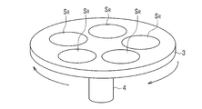
- 2A and 2B are perspective views showing an appearance of a mounting table as a support device used in the plasma processing apparatus 100.
- FIG. 3 is a schematic configuration diagram of a microwave introduction unit in the plasma processing apparatus 100.
- 4A, 4B, and 4C are plan views showing a planar antenna used in the plasma processing apparatus 100 of FIG.
- FIG. 5 is a bottom view showing the lower surface of the top wall 1c in the plasma processing apparatus 100 of FIG.
- the plasma processing apparatus 100 has, as main components, an airtight processing container 1 and a support apparatus 2 that supports a semiconductor wafer (hereinafter simply referred to as “wafer”) W as a target object in the processing container 1.
- a wave generator 39 and a control unit 50 as control means for controlling each component of the plasma processing apparatus 100 are provided. Note that the microwave introduction unit 27, the waveguide 37, and the microwave generator 39 constitute plasma generating means for generating plasma of the processing gas in the processing container 1.
- the processing container 1 has a bottom wall 1a, a side wall 1b and a top wall 1c made of a material such as aluminum.
- the support device 2 includes a mounting table 3, a support unit 4, and a drive device 5.
- the mounting table 3 horizontally supports a plurality of wafers W inside the processing container 1.
- the mounting table 3 is made of a material having high thermal conductivity, for example, a ceramic material such as AlN.
- the mounting table 3 is supported by a cylindrical support portion 4 that extends upward from the center of the bottom wall 1 a of the processing container 1.
- table 3 has, for example, a plurality of locations the depositing area S R for mounting thereon the wafer W as shown in FIG. 2A (five in FIG. 2A).
- the mounting table 3 is configured to be rotatable about the support portion 4 as a rotation axis (center) by a driving device 5 connected to the support portion 4.
- a plurality of mounting regions S R are arranged concentrically around the rotation axis of the table 3.
- FIG. 2B shows a modification of the mounting table in which five bases 8 supported by five support portions 7 are provided on a common base portion 6 configured to be rotatable by the driving device 5.
- the five support portions 7 and the pedestal 8 revolve around the same circumference around the rotation axis of the pedestal 6.
- the support device includes a base part 6, a support part 7, a base 8, and a drive device 5.
- the mounting table 3 is provided with a heating or cooling mechanism (not shown) so that the temperature of the wafer W can be controlled in a range from 25 ° C. (room temperature) to 900 ° C., for example.
- the mounting table 3 is provided with wafer support pins (not shown) for supporting the wafer W and raising and lowering it.
- Each wafer support pin is provided so as to protrude and retract with respect to the surface of the mounting table 3.
- a gas introduction part 15 is provided in the center of the top wall 1c of the processing container 1.
- the gas introduction part 15 has a cylindrical nozzle 16, and a gas hole 16 a is formed on the lower surface thereof. This gas introduction part 15 is connected to a pipe 17.
- the gas supply device 18 includes a gas supply source 18a and a pipe 17 connected to the gas supply source 18a. Although one gas supply source 18a and piping 17 are illustrated in FIG. 1, a plurality of gas supply sources 18a and piping 17 can be provided depending on the gas type.
- the gas supply source 18a supplies a processing gas such as a rare gas such as Ar, Kr, Xe, or He for plasma generation, an oxidizing gas such as an oxygen gas in oxidation treatment, or a nitriding gas in nitridation treatment.
- a film forming material gas In the case of a CVD process, a film forming material gas, a purge gas such as N 2 or Ar used for replacing the atmosphere in the processing container, and a cleaning such as ClF 3 or NF 3 used for cleaning the inside of the processing container 1 are used. It can also be configured to supply gas.
- a mass flow controller and an opening / closing valve In the middle of the pipe 17 connecting the gas supply source 18a to the gas introduction part 15, a mass flow controller and an opening / closing valve (not shown) are provided so that the supplied gas can be switched and the flow rate can be controlled.
- the gas supply device 18 may be a constituent part of the plasma processing apparatus 100 or an external device.
- a loading / unloading port 19 for loading / unloading the wafer W between the plasma processing apparatus 100 and a transfer chamber (not shown) adjacent thereto is provided, and this loading / unloading port 19 is provided.
- a gate valve 20 for opening and closing is provided on the side wall 1b of the processing chamber 1, a loading / unloading port 19 for loading / unloading the wafer W between the plasma processing apparatus 100 and a transfer chamber (not shown) adjacent thereto.
- a plurality of (two in FIG. 1) exhaust ports 11 are formed in the bottom wall 1a of the processing container 1.
- An exhaust pipe 12 is connected to the exhaust port 11, and is connected to an exhaust device 24 via the exhaust pipe 12.
- two exhaust ports 11 are provided in the bottom wall 1a, and an exhaust device 24 is connected to each.
- the exhaust device 24 includes, for example, an APC valve and a turbo molecular pump as a high-speed vacuum pump. As described above, the exhaust device 24 is connected to the exhaust port 11 via the exhaust pipe 12. By operating the exhaust device 24, the gas in the processing container 1 is exhausted to the outside through the exhaust port 11 and the exhaust pipe 12. Thereby, it is possible to depressurize the inside of the processing container 1 at a high speed, for example, to 0.133 Pa.
- the plasma processing apparatus 100 is configured to supply the microwaves generated by the plurality of microwave generators 39 into the processing container 1 via the microwave introduction units 27, respectively.
- the microwave generator 39 and the microwave introduction unit 27 are connected to each other by a waveguide 37.
- the microwave introduction unit 27 as an electromagnetic wave introduction unit will be described.
- the microwave introduction unit 27 includes a transmission plate 28 and a planar antenna 31 as main components.
- a transmission plate 28 as an electromagnetic wave introduction window that transmits microwaves is provided on a support portion 13a formed on the top wall 1c.
- a portion facing the inside of the processing container 1 between the support portions 13a is a microwave transmission region as an electromagnetic wave transmission region.
- the transmission plate 28 is made of a dielectric, for example, ceramics such as quartz, Al 2 O 3 , and AlN.
- a gap between the transmission plate 28 and the support portion 13a is hermetically sealed through a seal member 29. Accordingly, each transmission plate 28 closes the opening of the top wall 1c, and the airtightness in the processing container 1 is maintained.
- Planar antenna 31 above the transmission plate 28 is disposed so as to face the mounting region S R of the table 3.
- the planar antenna 31 has a disk shape.
- the shape of the planar antenna 31 is not limited to a disk shape, and may be a square plate shape, for example.
- the planar antenna 31 is made of, for example, a copper plate or an aluminum plate having a surface plated with gold or silver.
- the planar antenna 31 has a plurality of slot-shaped microwave radiation holes 32 that radiate microwaves. The microwave radiation holes 32 are formed through the planar antenna 31 in a predetermined pattern.
- the individual microwave radiation holes 32 have an elongated rectangular shape (slot shape), for example, as shown in FIG. 4A.
- the microwave radiation hole 32 may have another shape such as a circular shape or an arc shape.
- the arrangement form of the microwave radiation holes 32 is not particularly limited.
- a plurality of curved and elongated microwave radiation holes 32 may be arranged in a circular shape as a whole.
- the elongated microwave radiation holes 32 may be arranged so as to extend radially from the center of the planar antenna 31.
- the lower end of the waveguide 37 is connected on the planar antenna 31.
- a microwave generator 39 that generates microwaves is connected to the other end of the waveguide 37 via a matching circuit 38.
- a microwave generator 39 as an electromagnetic wave generator generates a microwave having a predetermined frequency.
- the microwave frequency for example, 2.45 GHz is preferably used, and 800 MHz to 1 GHz (preferably 800 MHz to 915 MHz), 8.35 GHz, 1.98 GHz, and the like can also be used.
- the waveguide 37 extends in a horizontal direction connected to the upper end portion of the circular waveguide 37a via the mode converter 40, and a circular waveguide 37a having a circular cross section extending upward from the planar antenna 31. And a rectangular waveguide 37b.
- the mode converter 40 has a function of converting the microwave propagating in the TE mode in the rectangular waveguide 37b into the TM mode. With such a structure, the microwave is propagated to the planar antenna 31 via the circular waveguide 37a having an inner conductor (not shown).
- the microwave generated by the microwave generator 39 is propagated to the planar antenna 31 of the microwave introduction unit 27 through the waveguide 37 and further through the microwave transmission region of the transmission plate 28. It is introduced into the processing container 1.
- the mechanism for introducing the microwave into the processing container 1 is not limited to the configuration illustrated in FIG.
- the microwave introduction mechanism disclosed in Patent Document 5 can also be suitably used.
- FIG. 5 is a bottom view of the top wall 1 c as viewed from the inside of the processing container 1.
- a total of 20 transmission plates 28 are depicted. That is, a total of 20 microwave introduction units 27 are provided in the plasma processing apparatus 100 of the present embodiment.
- the configuration of each microwave introduction unit 27 is the same, and the area of the transmission plate 28 is also equal.
- the arrangement of the microwave introduction unit 27 will be described according to the position of the transmission plate 28.
- the transmission plate 28 serving as the electromagnetic wave introduction window is not limited to a circle, and may be another shape such as a rectangle.
- five transmission plates 28 are concentrically arranged so as to surround the center O of the top wall 1c (here, the same as the position of the rotation axis of the mounting table 3). Are arranged in quadruplicate in the radial direction (the radial direction of the mounting table 3).
- the first innermost circumference is composed of five transmission plates 28A1, 28B1, 28C1, 28D1, and 28E1.
- the second circumference from the inside is constituted by five transmission plates 28A2, 28B2, 28C2, 28D2, and 28E2.
- the third circumference from the inside is constituted by five transmission plates 28A3, 28B3, 28C3, 28D3, and 28E3.
- the 4th outermost periphery is comprised by five permeation
- the transmission plates 28A1 to 28A4 constitute one group from the viewpoint of performing plasma processing on one wafer W, and similarly, the transmission plates 28B1 to 28B4, the transmission plates 28C1 to 28C4, and the transmission plate 28D1.
- To 28D4 and transmission plates 28E1 to 28E4 also form groups. This point will be further described with reference to FIG.
- FIG. 6 shows the same arrangement of the transmission plates 28 as in FIG.
- the mounting table 3 depositing area S R mounting for mounting the wafer W is provided at five positions.
- Stage 3 by driving the driving device 5, for rotating (rotation) in the direction indicated by the arrow in FIG. 6, each mounting area S R is centered on the rotational axis of the table 3, the same direction To go around (revolution).
- the group transmission plates 28A1 ⁇ 28A4 from innermost transmission plate 28A1, to the outermost transparent plate 28A4 are aligned in sequence on the circumferential direction of the mounting area S R, arcuate Is arranged.
- the transmission plate 28A1 ⁇ 28A4, respectively, while the respective mounting area S R moves, are arranged to overlap vertically with respect to at least a portion thereof which mounting area S R.
- the placement area S R to the wafer W mounted is moved relative to the transmission plate 28A1 ⁇ 28A4, it passes through at least one position opposite the microwave transmissive area of in the transmission plate 28A1 ⁇ 28A4 It is configured.
- the wafer W is configured to move relative to the transmission plates 28A1 to 28A4 and pass through all the opposed positions of the microwave transmission regions of the transmission plates 28A1 to 28A4.
- the “opposite position” means that when the area of the microwave transmission region of the transmission plates 28A1 to 28A4 is projected vertically toward the mounting table 3 as it is, the projection region and the mounting region S R (or there) Means that the wafer W) placed at least partially overlaps.
- the transmission plates 28A1 to 28A4 are arranged so that the integrated value of the plasma density with time and / or the integrated value of the plasma irradiation time are the same at any position on the wafer W. Such an arrangement, the transmitting plate 28A1 ⁇ 28A4 sequentially at different times, will overlap a portion or entirety the mounting area S R vertically.
- each group of the transmission plates 28B1 to 28B4, the transmission plates 28C1 to 28C4, the transmission plates 28D1 to 28D4, and the transmission plates 28E1 to 28E4 is also arranged in an arc shape, and a part or all of them are mounted sequentially at different times. vertically and depositing area S R are arranged so as will overlap.
- the integrated time value of plasma irradiation in each part of the wafer W after the mounting table 3 is rotated a predetermined number of times is made the same, and the interval between the plurality of wafers W is increased.
- the plasma treatment can be performed almost uniformly in the plane of the wafer W. In other words, the irradiation time of the plasma generated by the microwave radiated from the microwave transmission region of the transmission plate 28 and acting on the wafer W is almost equal if time-averaged at any part of the surface of the wafer W.
- the plasma generated immediately below the microwave transmission region of the transmission plate 28 diffuses, so that the plasma reaching the surface of the wafer W is larger than the area of the microwave transmission region of the transmission plate 28. Will also have a large area (horizontal cross-sectional area).
- the area of the plasma diffusion region varies depending on the distance (gap L G ) from the transmission plate 28 to the surface of the wafer W.
- the arrangement of the transmission plate 28 can be determined in consideration of such plasma diffusion.
- the control unit 50 is a computer, and includes a controller 51 having a CPU, a user interface 52 connected to the controller 51, and a storage unit 53, as shown in FIG.
- the controller 51 is a component (for example, the driving device 5, the gas supply device 18, the exhaust device 24, the microwave generation device 39) related to process conditions such as gas flow rate, pressure, and microwave output. Etc.).
- the user interface 52 includes a keyboard on which a process manager manages command input to manage the plasma processing apparatus 100, a display for visualizing and displaying the operating status of the plasma processing apparatus 100, and the like.
- the storage unit 53 stores a recipe in which a control program (software) for realizing various processes executed by the plasma processing apparatus 100 under the control of the controller 51 and processing condition data are recorded. .
- an arbitrary recipe is called from the storage unit 53 according to an instruction from the user interface 52 and is executed by the controller 51, so that the controller 51 controls the plasma processing apparatus 100 in the processing container 1. Desired processing is performed.
- the recipes such as the control program and processing condition data may be stored in a computer-readable recording medium 54 or may be transmitted from another device at any time via a dedicated line, for example. It can also be used online. Examples of the computer-readable recording medium 54 include a CD-ROM, hard disk, SSD, flexible disk, flash memory, DVD, and Blu-ray disk.
- a command is input from the user interface 52 to perform plasma nitridation processing in the plasma processing apparatus 100.
- the controller 51 reads the recipe stored in the storage unit 53 or the recording medium 54.
- control is performed from the controller 51 to each end device of the plasma processing apparatus 100 such as the driving device 5, the gas supply device 18, the exhaust device 24, and the microwave generator 39 so that the plasma nitriding process is executed under conditions based on the recipe.
- a signal is sent out.
- the transfer port 19 and the gate valve 20 is opened, for example, sequentially transferring the plurality of wafers W into the processing chamber 1 and placed on the placement area of the mounting table 3 S R.
- the driving device 5 is driven to rotate the mounting table 3 and stabilized until a constant rotational speed is reached.
- the exhaust device 24 is operated to exhaust the inside of the processing container 1 under reduced pressure
- the rare gas and the nitrogen-containing gas are respectively supplied from the gas supply device 18 at a predetermined flow rate into the processing container 1 through the gas introduction unit 15. Introduce. Further, the inside of the processing container 1 is adjusted to a predetermined pressure by adjusting the exhaust amount and the gas supply amount.
- each microwave generator 39 is turned on to generate microwaves.
- microwaves having a predetermined frequency for example, 2.45 GHz
- the respective microwave generators 39 are guided from the respective microwave generators 39 to the waveguides 37 through the matching circuits 38, and are passed through the rectangular waveguides 37b and 37a. It passes through sequentially and is supplied to the planar antenna 31.
- the microwave propagates in the TE mode in the rectangular waveguide 37b, and the TE mode microwave is converted into the TM mode by the mode converter 40, and the plane of the microwave introduction unit 27 is passed through the circular waveguide 37a. Propagating toward the antenna 31.
- the microwave is radiated from the microwave radiation hole 32, which is a hole formed through the planar antenna 31, to the space above the wafer W in the processing chamber 1 through the microwave transmission region of the transmission plate 28. In this way, microwaves are introduced into the processing container 1 from the respective microwave introduction units 27.
- 20 microwave introduction units 27 are arranged, and an electromagnetic field is formed in the processing container 1 by the microwaves introduced into the processing container 1 through each microwave introduction unit 27.
- an inert gas and a nitrogen-containing gas introduced into the processing container 1 are turned into plasma.
- the plasma excited by the microwave has a high density of, for example, 10 10 / cm 3 to 10 13 / cm 3 when the microwave is radiated from a large number of microwave radiation holes 32 of the planar antenna 31, and the wafer. In the vicinity of W, the plasma has a low electron temperature of about 2 eV or less.
- the high-density plasma formed in this way has little plasma damage due to ions or the like on the underlying film.
- the silicon surface of the wafer W is nitrided by the action of active species such as radicals or ions in the plasma to form a thin silicon nitride film SiN.
- active species such as radicals or ions in the plasma to form a thin silicon nitride film SiN.
- silicon can be oxidized by using an oxygen-containing gas instead of a nitrogen-containing gas, and a film can be formed by a plasma CVD method by using a film-forming material gas.
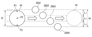
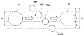
- L 1 indicates the adjacent ones of the transmission plates 28A1 to 28A4 in the direction perpendicular to the relative movement direction of the wafer W (or the direction perpendicular to the tangential direction when the relative movement direction is a circular orbit). (The distance between the centers of the microwave transmission regions of the transmission plates 28A1 to 28A4).
- M indicates the distance from the center of the innermost transmission plate 28A1 to the center of the outermost transmission plate 28A4, and D indicates the diameter of the wafer W.
- the arrows in the figure is a movement direction of the wafer W mounted on the fixed position of the depositing area S R placement for transmitting plate 28A1 ⁇ 28A4, the circumferential direction as shown in FIG. 6, the transmission plate 28A1 ⁇ 28A4 It is expressed linearly in consideration of the arcuate arrangement.
- the center position of the innermost transmission plate 28A1 and the position of the center of the microwave transmission region of the outermost transmission plate 28A4 are different from each other in the integrated value of plasma density at the end positions P1 and P3 of the wafer W.
- M is equal to or larger than the diameter D of the wafer W. That is, it is preferable that the relationship of M ⁇ D is satisfied.
- M D
- M> D the arrangement of the transmission plates 28A1 to 28A4 is preferably in FIG. 8B.
- the microwave transmission regions of two or more transmission plates of the transmission plates 28A1 to 28A4 and the wafer W are relatively moving. At the same time, they can overlap each other.
- the distance L 1 in the direction perpendicular to the relative movement direction of the transmission plates 28A1 to 28A4 arranged adjacent to each other in the relative movement direction (or the direction perpendicular to the tangential direction when the relative movement direction is a circular orbit).
- P1 passes just below the microwave transmission region of the transmission plate 28A1
- P3 passes just below the microwave transmission region of the transmission plate 28A4
- P2 and the transmission plate 28A2 Since P2 passes directly under both microwave transmission regions of the transmission plate 28A3, the plasma irradiation time of P2 is longer than that of P1 and P3.
- the plasma density of the transmission plates 28A1 to 28A4 is uniform, in P2, for example, in the nitriding process, the nitrogen dose amount and the nitride film thickness become larger than P1 and P3.
- the size and interval L 1 of the transmission plates 28A1 to 28A4 and the shortest distance from the transmission plates 28A to 28D to the surface of the wafer W (P1, P2, and P3 so that the integrated values of plasma density over time are the same)
- the gap L G ), the microwave power of each microwave introduction unit 27, and the like are adjusted. Further, by arranging the plasma source (transmission plate) so that the time integrated value of plasma irradiation is the same at any position on the wafer W, more uniform processing can be performed.
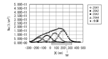
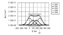
- FIG. 9 to FIG. 14 show the results of simulating the overlap of temporal integration values of plasma density when four transmission plates 28A1 to 28A4 (diameter 109 mm) are arranged at a predetermined interval, as in FIG. 8A or FIG. 8B. Show.
- the shortest distance (gap L G ) from each transmission plate 28A1 to 28A4 to the surface of the wafer W was 89 mm.
- the diameter D of the wafer W was 300 mm.
- the vertical axis in FIGS. 9 to 14 shows the average value obtained by dividing the time integrated value of the electron density (plasma density) by the passage time, and the horizontal axis shows the distance in the direction perpendicular to the moving direction of the wafer W. Yes. Further, the horizontal axis of FIGS. 9 to 14 shows the size (diameter) of the wafer W in an overlapping manner.
- the wafer W in a direction orthogonal to the relative movement direction between the wafer W and the transmission plate (when the relative movement direction is a circular orbit, it means a direction orthogonal to the tangential direction; the same applies hereinafter).
- the central part is high, the end part is depressed, and the whole part has a mountain shape.
- the sum of the plasma densities of the central portion and the end portion of the wafer W in the direction orthogonal to the relative movement direction is substantially equal.
- the plasma density of the transmission plates 28A1 and 28A4 arranged at both ends falls on the outside.
- a drop occurs at a portion outside the width D of the wafer W, a substantially uniform plasma density is maintained in the plane of the wafer W.
- the case where the microwave power introduced from is changed is shown.
- FIG. 11 shows a case where the microwave power introduced from the transmission plates 28A1 and 28A4 arranged on the outside is 1000 W, and the microwave power introduced from the two transmission plates 28A2 and 28A3 arranged on the inside is 600 W. .
- the total value of the plasma density falls at the central portion of the wafer W in the direction orthogonal to the relative movement direction, and is higher at the end.
- FIG. 11 shows a case where the microwave power introduced from the transmission plates 28A1 and 28A4 arranged on the outside is 1000 W, and the microwave power introduced from the two transmission plates 28A2 and 28A3 arranged on the inside is 600 W. .
- the total value of the plasma density falls at the central portion of the wafer W in the direction
- FIG. 12 shows a case where the microwave power introduced from the transmission plates 28A1 and 28A4 arranged on the outside is 1000 W, and the microwave power introduced from the two transmission plates 28A2 and 28A3 arranged on the inside is 1300 W. .
- the total value of the plasma density is high at the central portion of the wafer W in the direction orthogonal to the relative movement direction and low at the end portion.
- FIG. 13 shows a case where the microwave power to be introduced is set to 400 W, 600 W, 800 W, and 1000 W in the order of the transmission plates 28A1, 28A2, 28A3, and 28A4.
- the total value of the plasma density is high on one end side (transmission plate 28A4 side) of the wafer W in the direction orthogonal to the relative movement direction, falls on the multi-end side (transmission plate 28A1 side), and a gradient in one direction occurs.
- the microwave power introduced from the transmission plates 28A1 and 28A4 disposed on the outside is increased to 1000 W each, and the microwave power introduced from the two transmission plates 28A2 and 28A3 disposed on the inside is decreased to 700 W each. ing.
- M ⁇ D the drop in the combined value of the plasma density at the end of the wafer W in the direction orthogonal to the relative movement direction is not improved.
- a plurality of mounting region S R for placing the wafer W, the mounting of the plurality of depositing area S respectively placed R wafers W is, Relative movement is possible so as to pass through a position opposite to the microwave transmission region of the transmission plate 28 of at least one microwave introduction unit 27. Further, by arranging the plasma source (transmission plate) so that the integrated value of the plasma density and / or the integrated value of the plasma irradiation time are the same at any position on the wafer W, uniform processing is possible. Become. Accordingly, it is possible to improve the uniformity of processing between a plurality of wafers W and within the surface of one wafer W.
- the plasma distribution in the processing chamber 1 can be controlled independently without replacing the planar antenna 31 or changing the process conditions. Therefore, the plasma can be stably maintained in a desired distribution in the processing container 1. Further, even when the processing container 1 is increased in size in response to an increase in the size of the wafer W, the plasma distribution generated in the processing container 1 can be easily adjusted by changing the number and arrangement of the microwave introduction units 27. .
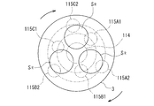
- the arrangement of the microwave introduction unit 27 will be described with some examples. Also here, the arrangement of the microwave introduction unit 27 is shown by the transmission plate. 15 to 24, the arrangement of the transmission plate 28 is projected on the plan view of the mounting table 3. In the example below, it is three or five depicting placement area S R, the number of mounting regions S R is arbitrary.
- the first innermost circumference is constituted by three transmission plates 111A1, 111B1, and 111C1.
- the second circumference from the inside is constituted by three transmission plates 111A2, 111B2, and 111C2.
- the third circumference from the inside is constituted by three transmission plates 111A3, 111B3, and 111C3.
- the 4th outermost periphery is comprised by three permeation
- the transmission plates 111A1 to 111A4 form one group from the viewpoint of performing plasma processing on one wafer W. Similarly, the transmission plates 111B1 to 111B4 and the transmission plates 111C1 to 111C4 also form groups. Yes. Transmitting plate 111A1 ⁇ 111A4 of each group, transmission plate 111B1 ⁇ 111B4, transmitting plate 111C1 ⁇ 111C4, respectively, the arc from the inside to the outside, and arranged in sequence on the circumferential direction of the depositing area S R mounting indicated by the arrow ing.
- transmission plate 111A1 ⁇ 111A4 of each group, transmission plate 111B1 ⁇ 111B4, transmitting plate 111C1 ⁇ 111C4 are arranged across the width of the mounting region S R (radial circular orbit circling). Such sequences, sequentially staggered relative placement area S R, are arranged such that a portion or all of the plurality of the transmission plate is gradually overlapped vertically.
- the basic concept of the arrangement shown in FIG. 15 is the same as in FIGS. 5 and 6, but in FIG. 15, the number of groups is smaller than in FIGS.
- the plasma source transmission plate
- the number of transmission plates disposed is the size of the processing container 1, the number of mounting regions S R (or wafers W), the rotation speed of the mounting table 3, and the content of processing (for example, oxidation, nitridation, film formation, etching). Etc.) and the like.
- a transmission plate 112 having a larger diameter than the surrounding transmission plates 113A1 to 113A3, 113B1 to 113B3, 113C1 to 113C3 is provided.
- transmission plates 113A1, 113B1, and 113C1 are provided in the first circumference from the inside
- 113A2, 113B2, and 113C2 are provided in the second circumference
- the transmission plates 113A3, 113B3, and 113C3 are provided in the third circumference.
- the transmission plates 113A1 to 113A3 constitute one group from the viewpoint of performing plasma processing on one wafer W by combining with the transmission plate 112, and similarly, the transmission plates 113B1 to 113B3 and the transmission plates 113C1 to 113C3. Also, a group is formed by combination with the transmission plate 112.
- the transmission plate 113A1 ⁇ 113A3 of each group, transmission plate 113B1 ⁇ 113B3, transmitting plate 113C1 ⁇ 113C3, respectively, are arranged across the width of the mounting region S R (radial circular orbit circling).
- Such sequences, sequentially staggered relative placement area S R, are arranged such that a portion or all of the microwave transmission regions of the plurality of the transmission plate is gradually overlapped vertically.
- the inner side (rotation axis side) of the mounting region S R (or the wafer W) that makes a circular motion always overlaps directly below the microwave transmission region of the transmission plate 112 at any position on the circular track. Therefore, the plasma density on the inner side (rotation axis side) of the mounting region S R (or the wafer W) can be made higher than that on the outer side.
- FIG. 17 shows an example in which one of the transmission plates in each group in FIG. 16 is omitted and the number of transmission plates is reduced. Although depicts three of the depositing area S R mounting 17, the number of mounting regions S R is arbitrary.
- a large-diameter transmission plate 114 is provided at the center of the top wall 1c.
- three transmitting plate 115A1,115B1 and 115C1 from the inside to the first round, but provided in the second round transparent Three plates 115A2, 115B2, and 115C2 are provided, and a total of seven transmission plates are provided.
- the transmission plates 115A1 and 115A2 constitute one group from the viewpoint of performing plasma processing on one wafer W by combining with the transmission plate 114.
- the transmission plates 115B1 and 115B2 and the transmission plates 115C1 and 115C2 are formed.
- a group is configured by combination with the transmission plate 114.
- the transmission plate 115A1,115A2 of each group, transmission plate 115B1,115B2, transmitting plate 115C1,115C2, respectively, are arranged across the width of the mounting region S R (radial circular orbit circling).
- the inside of the mounting orbiting motion depositing area S R or the wafer W (rotating shaft side) is at any position on the orbit, always overlaps directly below the microwave transmissive area of the transmissive plate 114. Accordingly, the plasma density of the inner (rotary shaft side) in the mounting area S R or the wafer W, can be higher than the outside.
- the first innermost circumference is constituted by three transmission plates 116A1, 116B1, and 116C1.
- the second circumference from the inside is constituted by three transmission plates 116A2, 116B2, and 116C2.
- the third circumference from the inside is constituted by four transmission plates 116A3, 116B3, 116C3, and 116D.
- the fourth outermost circumference is composed of six transmission plates 116A4, 116B4, 116C4, 116E, 116F, and 116G.
- the first innermost circumference is composed of two transmission plates 117A and 117B.
- the second circumference from the inside is constituted by two transmission plates 118A and 118B.
- the third circumference from the inside is constituted by two transmission plates 119A and 119B.
- the 4th outermost periphery is comprised by four transmissive plates 120A, 120B, 120C, and 120D.
- the area of the transmission plate from the first to fourth rounds is changed, the first and fourth rounds are the same size, the second round is larger than the first round, The third lap is even larger than the second lap.
- transmission plates having different areas can be combined and arranged.
- a portion or all of the microwave transmission regions of the plurality of transparent plates relative placement region S R are sequentially staggered times, are arranged to continue to overlap vertically.
- the plasma source transmission plate is disposed at any position on the wafer W such that the integrated value of the plasma density and / or the integrated value of the plasma irradiation time are the same, thereby performing uniform processing. Is possible.
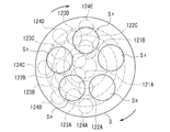
- Figure 20 is arranged in the top wall 1c, at a position facing the orbit of the mounting area S R, 4 weeks concentrically, the transmission plate of the total of 14, not the entire top wall 1c, to bias a portion
- the first innermost circumference is composed of two transmission plates 121A and 121B.
- the second circumference from the inside is constituted by three transmission plates 122A, 122B, and 122C.
- the third circumference from the inside is constituted by four transmission plates 123A, 123B, 123C, and 123D.
- the fourth outermost circumference is composed of five transmission plates 124A, 124B, 124C, 124D, and 124E.
- the transmission plate and the mounting area S R By relatively moving the transmission plate and the mounting area S R (or the wafer W), it is not necessary to provide the transmission plate over the entire top wall 1c, so that the transmission plate is partially unevenly distributed as shown in FIG. It may be provided.
- the plasma source transmission plate
- the integrated value of the plasma density and / or the integrated value of the plasma irradiation time are the same at any position on the wafer W. It becomes possible.
- a film thickness measuring device or a gas supply device may be used for other purposes. it can.
- the transmission plate in the top wall 1c, at a position facing the orbit of the mounting area S R, shows an example in which the transmission plate is arranged in the oval shape of nine. That is, the first innermost circumference is composed of three transmission plates 125A, 125B, and 125C. Next, the second circumference from the inside is constituted by three transmission plates 126A, 126B, and 126C. The third circumference from the inside is composed of three transmission plates 127A, 127B, and 127C.
- the longitudinal angles of the transmission plates 125A to 125C, 126A to 126C, and 127A to 127C are arbitrary, and the centers do not necessarily have to be arranged concentrically.
- the shape of the transmission plate is not necessarily limited to a circle, and may be an arbitrary shape such as an ellipse or a polygon such as a quadrangle or a rectangle.
- the plasma source (transmission plate) so that the integrated value of the plasma density and / or the integrated value of the plasma irradiation time are the same at any position on the wafer W, uniform processing can be performed. It becomes possible.
- the second circumference from the inside is constituted by two transmission plates 129A and 129B.
- the third circumference from the inner side, which is the outermost circumference, is composed of two transmission plates 130A and 130B.
- the transmission plates 129A and 129B on the second circumference are configured to have a larger area than the transmission plates 128A and 128B on the first circumference and the transmission plates 130A and 130B on the third circumference.
- the transmission plate 129A, 129B is formed larger than the area of the mounting area S R (or wafer W), the total transmission plate 129A, the mounting directly beneath the 129B depositing area S R (or wafer W) Are formed to overlap. Therefore, from the viewpoint of uniformity of processing within the surface of the wafer W, the transmission plates 129A and 129B are the main plasma generation units, and the first rotation transmission plates 128A and 128B, the third rotation transmission plate 130A, Reference numeral 130B denotes an auxiliary plasma generation unit that complements the transmission plates 129A and 129B. In this case, by arranging the plasma source (transmission plate) so that the integrated value of the plasma density and / or the integrated value of the plasma irradiation time are the same at any position on the wafer W, uniform processing can be performed. It becomes possible.
- the microwave transmission regions of the transmission plates 128A and 128B and the transmission plates 130A and 130B functioning as auxiliary plasma generation units are partially up and down with the trajectory of the mounting region S R (or the wafer W). Although overlapping, it may be provided at a position deviating from the trajectory of the mounting region S R (or the wafer W) in consideration of plasma diffusion. Such an example is shown in FIG.
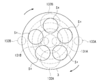
- the first innermost circumference is composed of two transmission plates 131A and 131B.
- the second circumference from the inside is constituted by two transmission plates 132A and 132B.
- the third circumference from the inner side which is the outermost circumference is constituted by two transmission plates 133A and 133B.
- the second round transmission plates 132A and 132B are configured to have a larger area than the first round transmission plates 131A and 131B and the third round transmission plates 133A and 133B.
- the transmission plate 132A, 132B is, the mounting is formed larger than the area of the depositing area S R (or wafer W), a large transmission plates 132A, mounting directly beneath the 132B depositing area S R (or wafer W) It is formed so that the parts overlap. Therefore, from the viewpoint of uniformity of processing within the surface of the wafer W, the transmission plates 132A and 132B are the main plasma generation units, and the transmission plates 131A and 131B on the first circumference, the transmission plates 133A on the third circumference, 133B is an auxiliary plasma generation unit that complements the transmission plates 132A and 132B.
- the transmission plates 133A and 133B that function as auxiliary plasma generation units do not partially overlap the trajectory of the placement region S R (or the wafer W), but the transmission plates 133A. Since the plasma generated immediately below the microwave transmission region of 133B diffuses above the wafer W by diffusion, it supplements the plasma generated by the microwave introduced from the microwave transmission region of the transmission plates 132A and 132B. An effect is obtained. In this case, by arranging the plasma source (transmission plate) so that the integrated value of the plasma density and / or the integrated value of the plasma irradiation time are the same at any position on the wafer W, uniform processing can be performed. It becomes possible.
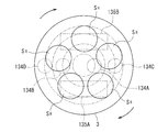
- FIG. 24 shows a configuration example in which a large area and a small area transmission plate are combined, as in FIG. That is, in a position facing the orbit of the mounting area S R in the top wall 1c, concentric to the two large-area transmission plate 135A, and 135B, 4 weeks concentrically, four transmission plate is disposed.
- the first innermost circumference of the small area transmission plate is the transmission plate 134A
- the second rotation from the inside is the transmission plate 134B
- the third rotation from the inside is the transmission plate 134C
- the fourth rotation from the innermost side is the outermost periphery.
- the large-area transmission plates 135 ⁇ / b> A and 135 ⁇ / b> B are configured in a rectangular shape in accordance with the shape of the waveguide 37.
- the transmission plate 135A, 135B is formed larger than the area of the mounting area S R (or wafer W), transmission plate 135A, immediately below the 135B, mounting area S R (or wafer W) is By relative movement, all of them are formed so as to pass directly below the microwave transmission region of the transmission plates 135A and 135B.
- the transmission plates 135A and 135B are the main plasma generation units, and the first rotation transmission plate 134A, the second rotation 134B, and the third rotation.
- the transmission plate 134C and the fourth circumference 134D are auxiliary plasma generation units that complement the transmission plates 135A and 135B.
- the transmission plates 134A, 134B, 134C, and 134D that function as an auxiliary plasma generation unit partially overlap the trajectory of the mounting region S R (or the wafer W) vertically. As described in the example of FIG.
- the transmission plates 134A, 134B, 134C, and 134D may be provided at positions deviating from the locus of the mounting region S R (or the wafer W). .
- the plasma source transmission plate
- FIG. 15 as shown in-FIG. 24, placement area S R (or wafer W) case of orbital movement and soon the rotary shaft in the mounting area S R (or wafer W)
- the movement speed is slow at the peripheral part, and the movement speed is high at the peripheral part. Therefore, as illustrated in FIG. 18, arranged a number of transmission plate outer portion than the inner portion of the top wall 1c, the moving speed is likely to increase the plasma density in the peripheral portion of the quick mounting area S R It is also effective.
- increasing the area of the transparent plate in the outer portion it is effective to moving speed is to increase the plasma density in the peripheral portion of the quick mounting area S R.
- the outer peripheral portion of the mounting movement speed is fast depositing area S R It is also effective to increase the plasma density.
- auxiliary plasma by placing the outer portion of the generator to become transparent plate top wall 1c, plasma in the peripheral section of the mounting movement speed is fast depositing area S R It is also effective to increase the density.
- the plasma source transmission plate
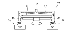
- FIG. 25 schematically shows the gas flow inside the processing container 1 of the plasma processing apparatus 100.
- the exhaust device 24 includes an APC valve (APC) and a turbo molecular pump (TMP).
- APC APC valve
- TMP turbo molecular pump
- FIG. 26 shows the positional relationship among the mounting table 3, the mounting region S R , the gas introducing unit 15, and the exhaust port 11 with respect to the gas flow in the processing container 1 in the same configuration of the gas introducing unit 15 as in FIG. 25.
- This is schematically shown as follows.
- the gas introduction part 15 is disposed in the center of the top wall 1 c, and one gas hole 16 is provided in the center of the gas introduction part 15.
- the exhaust port 11 is provided in an annular shape below the mounting table 3, the gas injected from the gas holes 16 is evenly distributed radially in the processing container 1 as indicated by arrows in the figure.
- the air is exhausted from the exhaust port 11.
- uniformly gas is distributed to the surface of the wafer W mounted on the depositing area S R mounting of the mounting table 3 to rotate, equalizing processing between a plurality of wafers W, and one wafer Processing in the W plane can be made uniform.
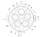
- FIG. 27 shows another configuration example of the gas introduction part and the exhaust part.
- the gas holes 16a are provided over the entire top wall 1c. That is, many gas holes 16a are formed over the entire area of the ceiling wall 1c except for the place where the transmission plate 28 (plasma introduction unit 27) of the ceiling wall 1c is provided.
- the configuration for introducing gas into each gas hole 16a may be, for example, a gas flow path formed inside the top wall 1c, or a gas distributor disposed on the top of the top wall 1c.
- the exhaust ports 11 are arranged at four locations below the mounting table 3, the gas injected from each gas hole 16 a is evenly distributed in the processing container 1 and exhausted from each exhaust port 11.
- uniformly gas is distributed to the surface of the wafer W mounted on the depositing area S R mounting of the mounting table 3 to rotate, equalizing processing between a plurality of wafers W, and one wafer Processing in the W plane can be made uniform.
- a more uniform gas flow can be obtained by installing an exhaust dispersion plate at the exhaust port 11.
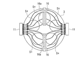
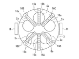
- the gas introduction unit includes, for example, a gas introduction member 16 that is provided facing the mounting table 3 and has a shape elongated in the radial direction of the mounting table 3.
- the gas introduction member 16 includes a nozzle for introducing gas.
- a plurality of gas holes 16 a are formed in series on the lower surface of the gas introduction member 16.
- the two gas introduction members 16 are linearly arranged so that their longitudinal directions overlap the diameter of the mounting table 3.
- the gas introduction member 16 is disposed at a position deviated from directly below the microwave introduction unit 27.
- the longitudinal direction of the gas introduction member 16 is arranged orthogonal to the traveling direction of the wafer W revolving on the circular orbit (that is, the tangential direction of the circular orbit).
- Gas is injected into a line shape toward the mounted wafer W (not shown) to the depositing area S R mounting of the table 3 from a plurality of gas holes 16a of the gas introducing member 16.
- the gas reaches the upper surface of the mounting table 3, flows in two directions, and travels toward the exhaust port 11 disposed below the outer peripheral portion of the mounting table 3.
- the exhaust port 11 is provided at a position shifted by approximately 90 ° from the arrangement position of the pair of gas introduction members 16 in the circumferential direction of the mounting table 3.
- a gas is supplied from the long gas introduction member 16 in a line form, by branching in two directions of flow just above the mounting table 3 rotating, a plurality placed on the placement area S R Reaction species and reaction products are evenly distributed between the wafers W as an integral value of rotation (revolution), so that the processing is uniform between the wafers W and the processing within the wafer W is uniform. Can be achieved.
- FIG. 29 shows a configuration example in which three sets (six in total) of gas introducing members paired in the longitudinal direction are arranged. That is, the gas introduction members 16 ⁇ / b> A and 16 ⁇ / b> A are arranged linearly so that their longitudinal directions overlap the diameter of the mounting table 3. Similarly, the gas introduction members 16B and 16B and the gas introduction members 16C and 16C are also arranged linearly so that their longitudinal directions overlap the diameter of the mounting table 3, respectively.
- the configuration of each gas introduction member 16 is the same as in FIG.
- the arrangement angles of the gas introduction members 16A, 16A and the gas introduction members 16B, 16B and the arrangement angles of the gas introduction members 16A, 16A and the gas introduction members 16C, 16C are arbitrary.
- the gas introduction members 16B and 16B and the gas introduction members 16C and 16C can be arranged at an angle shifted by 45 ° with respect to the gas introduction members 16A and 16A.
- the gas introducing member 16 is disposed in a plurality of positions of the top wall 1c of the processing chamber 1, by performing the gas supply, among a plurality of wafers W placed on the placement area S R
- the reaction species and reaction products are evenly distributed as an integral value of rotation (revolution), and it is possible to further achieve uniform processing between wafers W and uniform processing within a single wafer W surface.
- the number of the gas introduction members 16 can be further increased as compared with FIG.
- the gas type introduced via the gas introduction members 16A and 16A and the gas type introduced via the gas introduction members 16B and 16B and the gas introduction members 16C and 16C may be changed.
- a gas that generates a short-lived active species or a gas that generates reactive species that adversely affect the process when present in plasma for a long time is introduced separately from other gases from the gas introduction members 16A and 16A. You can also.
- a gas that generates a short-lived active species can be used efficiently, or a reactive species that adversely affects the process if present in the plasma for a long time. Generation can be suppressed.
- the gas types introduced from the gas introduction members 16A, 16B, and 16C can be all different types.
- FIG. 30 shows another configuration example of the gas introduction part and the exhaust part.
- a gas introduction member 16 ⁇ / b> D curved in an arc shape is provided as a gas introduction part.
- the exhaust port 11A also has a bowed shape.
- the gas introduction member 16D provided on one side upper part of the processing container 1 toward the exhaust port 11A provided on the one side lower part of the processing container 1 obliquely downward with the mounting table 3 interposed therebetween.
- a gas flow in almost one direction is formed.
- the configuration in FIG. 30 forms a unidirectional gas flow near the surface of the wafer W in the processing chamber 1. because it can, even for the outer of the wafer W with respect to the inner (rotation center side) of the wafer W to revolve placed on the placement area S R, there is a merit that it is possible to perform equally supply of gas.
- the gas introduction member 16 ⁇ / b> D and the exhaust port 11 ⁇ / b> A are provided along the inner surface (not shown) of the circular processing container 1.
- the configuration of the gas introduction part and the exhaust part in the plasma processing apparatus 100 is the size of the processing container 1, the arrangement of the microwave introduction unit 27, the area of the transmission plate 28, the placement region S R (or The number of wafers W), the rotation speed of the mounting table 3, the content of processing (for example, oxidation, nitridation, film formation, etching, etc.), etc.
- the configuration of the gas introduction part and the exhaust part as illustrated in FIGS. equally it is possible to distribute the gas to the surface of the third mounting region S placed R wafers W.
- the plasma source (transmission) is used so that the integrated value of the plasma density and / or the integrated value of the plasma irradiation time are the same at any position on the wafer W.
- uniform processing becomes possible. Accordingly, it is possible to achieve uniform processing among a plurality of wafers W and uniform processing within a single wafer W surface.
- Example 1 As shown in FIG. 31, a plasma processing apparatus was used in which transmission plates 28X, 28Y, and 28Z having a circular microwave transmission region having a diameter of 90 mm were linearly arranged on the top wall 1c. That is, microwave introduction units are provided at the positions of the transmission plates 28X, 28Y, and 28Z, respectively.
- the transmission plate 28X will be referred to as a “first plasma source 28X”, the transmission plate 28Y as a “second plasma source 28Y”, and the transmission plate 28Z as a “third plasma source 28Z”.
- the distance to the center of the second plasma source 28Y and the distance to the center of the third plasma source 28Z were set to 175 mm, respectively, using the center of the first plasma source 28X as a reference (zero). . Further, in this experiment, since the purpose is to evaluate the uniformity of the process, a single wafer W having a diameter of 300 mm was assumed as the object to be processed.
- Plasma was generated under the following conditions, and the plasma density was measured at a position 49 mm below the top plate 1c.
- ⁇ Plasma generation conditions> Ar gas flow rate: 1000 mL / min (sccm) N 2 gas flow rate; 200 mL / min (sccm) Processing pressure: 20 Pa Temperature of mounting table; room temperature (25 ° C) Each microwave power; First plasma source 28X ... 260W Second plasma source 28Y ... 260W Third plasma source 28Z ... 260W
- FIG. 32 shows the plasma density when the microwave introduction units of the first plasma source 28X, the second plasma source 28Y, and the third plasma source 28Z are individually operated, and when all are operated simultaneously. It is the graph which piled up and showed the plasma density of.
- the vertical axis represents the plasma density
- the horizontal axis represents the distance from the center of the first plasma source 28X serving as a reference.
- the width of the wafer W is indicated by a dotted line (the same applies to FIGS. 33 to 35).
- the plasma density is near the center of each plasma source (transmission plate).
- the microwave introduction units of the first plasma source 28X, the second plasma source 28Y, and the third plasma source 28Z are operated at the same time, they are almost constant (about 1 over the entire radial direction of the wafer W). It was confirmed that the plasma density was ⁇ 10 11 / cm 3 .
- the plot “combined (calculated)” is a sum of the calculated plasma densities of the first plasma source 28X, the second plasma source 28Y, and the third plasma source 28Z. It was almost consistent with the result of “synthesis (actual measurement)”.
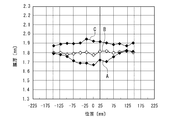
- FIG. 33 shows the results when only the microwave power of the microwave introduction unit of the first plasma source 28X is changed to 100 W, 260 W, or 500 W under the same conditions as in Experimental Example 1.
- the symbol A in the graph means that the microwave power of the microwave introduction unit of the first plasma source 28X is 100 W, the symbol B is 260 W, and the symbol C is 500 W.
- the case (B) in which the microwave power of the microwave introduction unit of the first plasma source 28X is 260 W is a reprint of Experimental Example 1.
- the plasma density is increased in the radial direction of the wafer W by increasing or decreasing the microwave power of the microwave introduction unit of the first plasma source 28X arranged at the center of the three. It became convex (C; 500 W) or convex downward (A; 100 W), and was confirmed to change. As a result, it was confirmed that when a plurality of microwave introduction units are provided, the intensity distribution of the synthesized plasma density can be controlled by changing the microwave power of each microwave introduction unit.
- Plasma nitriding treatment was performed on the silicon substrate as the wafer W under the following conditions, and the thickness of the silicon nitride film was measured. In addition, the distance (gap) from the top plate 1c to the wafer W was 85 mm.
- ⁇ Plasma nitriding conditions Ar gas flow rate: 1000 mL / min (sccm) N 2 gas flow rate; 200 mL / min (sccm) Processing pressure: 20 Pa Temperature of mounting table: 500 ° C Microwave power; Only the microwave power of the microwave introduction unit of the first plasma source 28X was changed to 100W, 260W, or 500W.
- the results are shown in FIG.
- the vertical axis in FIG. 34 indicates the optical film thickness (refractive index 2.0) of the silicon nitride film, and the horizontal axis indicates the distance from the center of the first plasma source 28X serving as a reference.
- the meanings of A, B, and C in the graph of FIG. 34 are the same as those in FIG. 34, silicon nitride films are uniformly formed in the radial direction of the wafer W when the microwave powers of the three microwave introduction units are set to be the same (B).
- the in-plane film thickness of the silicon nitride film is increased in the radial direction of the wafer W. It was confirmed that it changed from convex (C; 500 W) or downward (A; 100 W). From FIG. 34, a tendency similar to that of FIG. 33 can be seen. That is, it was confirmed that the measurement result of the plasma density in FIG. 33 corresponds to the measurement result of the film thickness of the silicon nitride film in FIG.
- Range / 2AVE that is, (maximum value of nitride film thickness ⁇ minimum value of nitride film thickness) / average value of nitride film thickness ⁇ 2] which is an index of in-plane uniformity is 4. 2%, B was 1.3%, and C was 1.9%. From the above results, when a plurality of microwave introduction units are arranged, the thickness of the silicon nitride film can be controlled in the plane of the wafer W by changing the microwave power of each microwave introduction unit. Was confirmed.
- Plasma nitridation was performed on the silicon substrate as the wafer W in the same manner as in Experiment 3 except that the microwave power of the microwave introduction units of the plasma sources 28X, 28Y, and 28Z was uniformly changed.
- the results are shown in FIG.
- the vertical axis in FIG. 35 indicates the optical film thickness (refractive index 2.0) of the silicon nitride film, and the horizontal axis indicates the distance from the center of the first plasma source 28X serving as a reference. Further, D, E, and F in the graph of FIG. 35 mean the plasma nitriding conditions. From FIG. 35, it is confirmed that when the microwave power of the three microwave introduction units is set to be the same, the distribution of the in-plane film thickness of the silicon nitride film on the wafer W shifts almost in parallel depending on the magnitude of the power. It was done.
- Range / 2AVE (maximum value of nitride film thickness ⁇ minimum value of nitride film thickness) / average value of nitride film thickness ⁇ 2] which is an index of in-plane uniformity of the wafer W of the silicon nitride film is:
- D was 1.06%
- E was 1.26%
- F was 0.85%, all of which were excellent values.
- ALD Atomic Layer Deposition
- MLD Molecular Layer Deposition
- ALD method As a film forming technique in a semiconductor manufacturing process, for example, a method called ALD (Atomic Layer Deposition), MLD (Molecular Layer Deposition), or the like (herein referred to as “ALD method”) is known.
- ALD method after the first reaction gas is adsorbed on the surface of the substrate in a vacuum atmosphere, the gas to be supplied is switched to the second reaction gas, and one or more atomic layers or A molecular layer is formed. By performing this cycle many times, these layers are stacked and film formation is performed on the substrate.
- the ALD method is an effective technique that can control the film thickness with high accuracy in accordance with the number of cycles and has good in-plane uniformity of the film quality and can cope with the thinning of semiconductor devices.
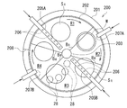
- FIG. 36 conceptually shows a configuration when the plasma processing apparatus of the present invention is applied to the ALD method.
- the film forming apparatus 200 includes a flat vacuum vessel 201 having a substantially circular planar shape, and a mounting table 202 provided in the vacuum vessel 201 and having a rotation center at the center of the vacuum vessel 201.
- the mounting table 202 is fixed to a cylindrical core 203 at the center, and the core 203 is fixed to a rotating shaft (not shown) extending in the vertical direction.
- the mounting table 202 and the core unit 203 are rotatable around a vertical axis (clockwise in this example).
- a circular mounting region S R for mounting the wafer W is provided as a recess. Note is depicted for convenience one mounting area S R only wafer W in FIG. 36. Mounting area S R is set slightly larger than the diameter of the diameter of the wafer W, also the magnitude of the equivalent thickness of the depth wafer W. The bottom of the mounting region S R, the lift pins are deployed in the through holes supporting the rear surface of the wafer W (not shown) for raising and lowering the wafer W.
- the inside of the vacuum vessel 201 is divided into a first region R1, a second region R2, a third region R3, and a fourth region R4.
- the first to fourth regions R1 to R4 are arranged in the first region R1, the second region R2, the third region R3, and the fourth region R4 from the upstream side to the downstream side in the rotation direction of the mounting table 202. Arranged in order.
- the boundary portion of each region is indicated by a line (reference symbol BR ), but the boundary of each region may be formed with a certain width (area).
- These first to fourth regions R1-R4, while allowing rotation of the mounting table 202, are separated by a boundary portion B R As can substantially block the atmosphere of each region.
- first to fourth regions R1-R4 As a means for separating the first to fourth regions R1-R4, respectively, details are omitted, for example, separates the boundary portion B R of each region of the first to fourth regions R1-R4 on the principle of the air curtain A configuration in which gas is introduced or a space between a ceiling surface (not shown) of the vacuum vessel 201 and the upper surface of the mounting table 202 is narrowly formed can be used in combination. Further, an exhaust port connected to a vacuum pump may be provided in each of the first to fourth regions R1 to R4.
- the first reaction gas nozzle 205A is provided at a position opposite to the passage area of the depositing area S R mounting the mounting table 202.
- the first reactive gas nozzle 205A is connected to a gas supply source (not shown) of DCS (dichlorosilane) gas that is the first reactive gas.
- a plurality of (for example, four) microwave introduction units are arranged in the third region R3.
- the position of the microwave introduction unit is indicated by the position of the transmission plate 28.
- the second reaction gas nozzle 205B is provided at a position opposite to the passage area of the depositing area S R mounting the mounting table 202.
- the second reactive gas nozzle 205B is connected to a gas supply source (not shown) of NH 3 gas that is the second reactive gas.
- gas discharge holes 206 for discharging the reaction gas are arranged in the lower side of the first reaction gas nozzle 205A and at intervals in the nozzle length direction.
- the first region R1 is a processing region for adsorbing the DCS gas to the wafer W
- the third region R3 is a processing region for adsorbing the activated NH 3 gas to the wafer W.
- the first reactive gas nozzle 205A and the second reactive gas nozzle 205B are attached to, for example, the side peripheral wall of the vacuum vessel 201.
- purge gas nozzles 207A and 207B for introducing a purge gas such as N 2 gas are provided in the second region R2 and the fourth region R4, respectively. These purge gas nozzles 207A and 207B are each connected to an N 2 gas supply source (not shown). The purge gas nozzles 207A and 207B are attached to the side peripheral wall of the vacuum vessel 201, for example.
- a plurality of exhaust ports are provided on the bottom wall of the vacuum vessel 201, and each exhaust port is connected to an exhaust device such as a vacuum pump via an exhaust pipe. Further, heating means such as a heater (not shown) is provided between the mounting table 202 and the bottom wall of the vacuum vessel 201 so that the wafer W can be heated to a predetermined temperature via the mounting table 202.
- a transfer port 208 for transferring a wafer W as a substrate between the transfer device (not shown) and the mounting table 202 is formed on the side wall of the vacuum vessel 201.
- the transfer port 208 is a gate valve (not shown). It can be opened and closed by. Depositing area S R mounting of the mounting table 202, the wafer W is transferred between the transport device (not shown) at a position facing to the transfer port 208.
- the silicon nitride film is formed as follows. First, the gate valve (not shown), and passes the placement region in S R of the mounting table 202 which is heating the wafer W, for example, in 200 ⁇ 400 ° C. through a transfer port 208 by an external transport device, not shown. This transfer is that placement area S R is lift pins (not shown) from the bottom side of the vacuum chamber 201 through the through hole of the bottom of the depositing area S R placement when stopped at the position facing the transfer port 208 lifting Is done. The delivery of such a wafer W, performs mounting table 202 intermittently rotated to place the respective wafers W within five mounting area S R of the mounting table 202.
- the gate valve is closed, and the inside of the vacuum vessel 201 is evacuated to a preset pressure by an exhaust device (not shown), and the wafer W is heated by a heater unit (not shown) while rotating the mounting table 202 clockwise.
- the DCS gas and the NH 3 gas are discharged from the first reaction gas nozzle 205 and the second reaction gas nozzle 205B, respectively, and the N 2 gas as the purge gas is discharged from the purge gas nozzles 207A and 207B.
- the wafer W alternately passes through the first region R1 in which the first reaction gas nozzle 205A is provided and the third region R3, which is a plasma generation unit, by the rotation of the mounting table 202, so that the DCS gas is adsorbed, The activated NH 3 gas is adsorbed, and these gas molecules react to form one or more silicon nitride molecular layers.
- silicon nitride molecular layers are sequentially stacked to form a silicon nitride film (SiN film) having a predetermined thickness.
- the DCS gas in the first region R1 and the NH 3 gas in the third region R3 are exhausted from exhaust ports (not shown) provided in the respective regions.
- the wafer W delivered from the first region R1 is purged in the second region R2, and the wafer W delivered from the third region R3 in the fourth region R4. Can be purged.
- the second region R2 and the fourth region R4 can also be used as separation regions for separating the first region R1 and the third region R3, and in this case, N 2 gas May be discharged in a line form from a long nozzle having a plurality of gas holes. In this way, the atmosphere in the first region R1 and the atmosphere in the third region R3 are completely separated, and the DCS gas and the NH 3 gas can be processed without being mixed.
- the plurality of wafers W are arranged in the rotation direction of the mounting table 202, and the mounting table 202 is rotated so that the first region R1 and the third region R3 In order, so-called ALD (or MLD) is performed.
- ALD or MLD
- a plurality of plasma sources transmission plate 28
- a temporal integration value of plasma density and / or plasma irradiation is performed at any position on the wafer W. Uniform processing is possible so that the integrated values of time are the same. Accordingly, it is possible to achieve uniform processing among a plurality of wafers W and uniform processing within a single wafer W surface.
- the ALD method is suitable for the purpose of forming a high dielectric film, such as a silicon nitride film (SiN film) or a silicon oxide film (SiO 2 film) used for a gate insulating film, for example, at a low temperature.
- a silicon nitride film SiN film
- a silicon oxide film SiO 2 film
- an example of forming a silicon nitride film has been given as an example.
- DCS gas as the first reaction gas
- oxygen gas or ozone gas as the second reaction gas
- a TiN film can be formed extremely thin at a low temperature by using TiCl 4 gas as the first reaction gas and NH 3 gas as the second reaction gas. is there.
- the area division in the film forming apparatus 200 is not limited to four.
- a Si film is formed in the first region, an oxidation (nitridation) process is performed in the third region, and a plasma modification process is performed on the silicon oxide film (silicon nitride film) in the fifth region. It is also possible. In this case, it is possible to perform processing by arranging a plurality of plasma sources (transmission plates 28) in one or both of the third region and the fifth region.
- the plasma processing apparatus of the present invention can be applied to, for example, a plasma oxidation processing apparatus, a plasma CVD processing apparatus, a plasma etching processing apparatus, a plasma ashing processing apparatus, etc. in addition to a plasma nitriding processing apparatus.
- the plasma processing apparatus 100 of the present invention is not limited to the case where the substrate as the object to be processed is a semiconductor wafer.
- the plasma processing apparatus 100 includes a substrate for a solar cell panel or a substrate for a flat panel display as an object to be processed. Applicable.
- the microwaves are individually supplied from a plurality of microwave generators to the plurality of microwave introduction units.
- a branched waveguide is provided from a single microwave generator. You may comprise so that a microwave may be supplied to two or more microwave introduction units.
- the microwave plasma processing apparatus is used.
- the present invention can also be applied to a plasma processing apparatus using a high frequency as an electromagnetic wave.
- a plasma generation method other types of plasma processing apparatuses such as an ICP plasma method, an ECR plasma method, a surface wave plasma method, and a magnetron plasma method can be used.
- a vacuum process but atmospheric pressure plasma can also be utilized.
- SYMBOLS 1 Processing container, 2 ... Support apparatus, 3 ... Mounting stand, 4 ... Support part, 11 ... Exhaust port, 15 ... Gas introduction part, 18 ... Gas supply apparatus, 24 ... Exhaust apparatus, 27 ... Microwave introduction unit, 28 ... transmission plate, 37 ... waveguide, 39 ... microwave generator, 50 ... controller, 100 ... plasma processing apparatus, W ... semiconductor wafer (substrate), S R ... placing region
Landscapes
- Physics & Mathematics (AREA)
- Engineering & Computer Science (AREA)
- Plasma & Fusion (AREA)
- Chemical & Material Sciences (AREA)
- Analytical Chemistry (AREA)
- Plasma Technology (AREA)
Abstract
プラズマ処理装置100は、処理容器1と、複数のウエハWを支持する載置台3と、処理容器1内の複数箇所でプラズマを生成させるための電磁波を導入する複数のマイクロ波導入ユニット27を備えている。載置台3の載置領域SRにそれぞれ載置されたウエハWが、少なくとも一つのマイクロ波導入ユニット27の透過板28のマイクロ波透過領域の対向位置を通過するように相対移動可能に構成されている。透過板28は、ウエハ上のどの位置においても、プラズマ密度の時間的積算値及び/又はプラズマ照射時間の積算値が同じになるように配置することができる。
Description
本発明は、処理容器へ所定周波数の電磁波を導き、プラズマを生成させて被処理体をプラズマ処理するプラズマ処理装置及びプラズマ処理方法に関する。
半導体ウエハなどの被処理体に対し、例えば酸化処理や窒化処理、CVD(Chemical Vapor Deposition)処理、エッチング処理などのプラズマ処理が行われる。プラズマ処理装置として、複数のスロットを有する平面アンテナを用いて処理容器内にマイクロ波を導入してプラズマを生成させるスロットアンテナ方式のプラズマ処理装置が知られている。また、他の方式のプラズマ処理装置として、コイル状のアンテナを用いて処理容器内に高周波を導入してプラズマを生成させる誘導結合型プラズマ(Inductively Coupled Plasma;ICP)方式のプラズマ処理装置が知られている。このようなプラズマ処理装置では、処理容器内で高密度のプラズマを生成させることが可能である。
次世代以降のデバイス開発に向けて、例えば3次元デバイス加工や微細化への対応を図りながら生産性を向上させるためには、基板面内における処理の均一性を確保しながら、複数の被処理体を処理したり、被処理体として現在300mm径である基板を450mm径に大型化させたりする必要がある。そのためには、基板に対応して大型化する処理容器内で、プラズマ密度の分布を均一化させる必要がある。
上記スロットアンテナ方式のプラズマ処理装置において、処理容器内で生成したプラズマの密度の制御は、スロットの形状や配置、処理容器やマイクロ波導入窓の形状設計などにより行われていた。例えば、処理内容に応じてプラズマ密度の分布を変えるためには、異なるスロット形状や配置の平面アンテナに交換することが必要である。また、上記ICP方式のプラズマ処理装置においても、プラズマ密度の分布を変えるためには、異なるコイル形状や配置のアンテナに変換することが必要である。しかし、このアンテナの交換は手間と時間を要する大掛かりな作業であった。
また、処理容器内で生成するプラズマ密度の分布は、例えば、マイクロ波のパワー、処理圧力、ガス流量などのプロセスパラメーターを変えることで微調整することも可能である。しかし、これらのプロセスパラメーターは、プロセス条件と切り離すことが出来ないため、プロセスパラメーターを変化させうる範囲でのプラズマ密度分布の変化幅(マージン)が小さく、その効果には限界があった。
また、平面アンテナ、処理容器などの製作公差、組み立て誤差、同一仕様の装置間での機差などの諸要因により、処理容器内でプラズマの対称性が崩れプラズマ密度の分布が偏心することがある。この場合も、これを簡易な方法で補正する手段がなかったため、平面アンテナの交換などの大掛かりな装置改変が必要になってしまうという問題があった。
ところで、複数の大型基板を同時に処理するために、複数のマイクロ波導入窓を設けるとともに、各マイクロ波導入窓に対応させて、それぞれの下方に試料台を設けたプラズマ処理装置が提案されている(例えば、特許文献1)。さらに、複数のマイクロ波導入窓からそれぞれマイクロ波を導入してプラズマを形成することにより、一枚の大型の基板に対して均一なプラズマ処理を行うようにしたプラズマ処理装置も提案されている(例えば、特許文献2)。また、複数のアンテナと複数のマイクロ波導入窓を有する装置において、アンテナ毎に異なる電力のマイクロ波を供給できるようにしたプラズマ処理装置も提案されている(例えば、特許文献3)。
また、複数の処理工程を効率的に行うために、処理容器内に隔壁によって分割された複数の処理室を設け、その下方に複数の基板を載置する載置台を回転可能に配備した処理装置も提案されている(例えば、特許文献4)。
また、スロットアンテナ方式のプラズマ処理装置において、処理容器内にマイクロ波を導入する機構として、スラグチューナによりマイクロ波の位相を変化させることができるように構成された複数のアンテナモジュールを用いるプラズマ処理装置も提案されている(例えば、特許文献5)。
処理容器内におけるプラズマ密度の分布を調整するためには、処理容器内で複数のプラズマを独立して生成させることが有効であると考えられる。しかし、各プラズマの生成部位と被処理体の配置が固定的であると、隣接するプラズマどうしの距離や、プラズマの拡散の程度によって、プラズマ密度に高低の分布が生じ、被処理体の面内における処理の均一化を図ることがかえって難しくなる、という課題があった。
本発明の目的は、処理容器内で複数のプラズマを生成させる方式のプラズマ処理装置において、プラズマ密度の分布の制御を容易にして、被処理体の面内で所望の処理を実現することである。
本発明のプラズマ処理装置は、被処理体を処理する処理空間を形成する真空引き可能な処理容器と、
前記処理容器内において被処理体を支持する支持装置と、
前記処理容器内でプラズマを生成させるための電磁波を発生させる電磁波発生装置と、
前記電磁波発生装置で発生した電磁波を前記処理容器内に導入する複数の電磁波導入ユニットと、
前記支持装置の中央を回転中心として、該支持装置に支持された複数の被処理体及び/又は前記複数の電磁波導入ユニットを回転させて、周回運動させる駆動装置と、
を備え、
前記電磁波導入ユニットは、前記処理空間に臨んで設けられた、電磁波を透過させて前記処理容器内に導入する電磁波導入窓を有しており、
前記支持装置は、複数の被処理体を載置する載置台を有しており、
前記載置台に載置された複数の被処理体が前記電磁波導入窓に対して相対移動し、それぞれの被処理体が少なくとも一つの前記電磁波導入窓の電磁波透過領域の対向位置を通過するように構成されている。
前記処理容器内において被処理体を支持する支持装置と、
前記処理容器内でプラズマを生成させるための電磁波を発生させる電磁波発生装置と、
前記電磁波発生装置で発生した電磁波を前記処理容器内に導入する複数の電磁波導入ユニットと、
前記支持装置の中央を回転中心として、該支持装置に支持された複数の被処理体及び/又は前記複数の電磁波導入ユニットを回転させて、周回運動させる駆動装置と、
を備え、
前記電磁波導入ユニットは、前記処理空間に臨んで設けられた、電磁波を透過させて前記処理容器内に導入する電磁波導入窓を有しており、
前記支持装置は、複数の被処理体を載置する載置台を有しており、
前記載置台に載置された複数の被処理体が前記電磁波導入窓に対して相対移動し、それぞれの被処理体が少なくとも一つの前記電磁波導入窓の電磁波透過領域の対向位置を通過するように構成されている。
また、本発明のプラズマ処理装置は、前記相対移動の間に、一つの被処理体が、2つ以上の前記電磁波導入窓に対して少なくとも部分的に対向する位置を順次通過するように構成されていてもよい。
また、本発明のプラズマ処理装置は、前記相対移動の間に、一つの被処理体が、同時に2つ以上の前記電磁波導入窓に対して少なくとも部分的に対向する位置を通過するように構成されているものであってもよい。
また、本発明のプラズマ処理装置において、前記複数の電磁波導入窓は、各電磁波導入窓から導入される電磁波によって生成するプラズマによる、プラズマ密度の時間的積算値及び/又はプラズマ照射時間の積算値が、一つの被処理体のどの位置においても同じになるように配置されていてもよい。
また、本発明のプラズマ処理装置は、前記相対移動する被処理体の軌道に対し、対向する位置から外れた位置に設けられた電磁波導入窓を有する補助的な電磁波導入ユニットを、さらに備えていてもよい。
また、本発明のプラズマ処理装置は、前記電磁波導入窓の面積が異なる複数の電磁波導入ユニットを備えていてもよい。
また、本発明のプラズマ処理装置は、前記電磁波発生装置が、前記電磁波導入ユニットに対して個別に設けられていてもよい。
また、本発明のプラズマ処理装置は、前記複数の電磁波導入ユニットに供給する電磁波のパワーが、個別に設定可能であってもよい。
また、本発明のプラズマ処理装置は、前記回転中心に近い位置にある内側の電磁波導入窓から導入される電磁波のパワーと、該内側の電磁波導入窓より周回半径の外側に位置する外側の電磁波導入窓から導入される電磁波のパワーと、が異なっていてもよい。
本発明のプラズマ処理方法は、被処理体を処理する処理空間を形成する真空引き可能な処理容器と、前記処理容器内において被処理体を支持する支持装置と、前記処理容器内でプラズマを生成させるための電磁波を発生させる電磁波発生装置と、前記電磁波発生装置で発生した電磁波を前記処理容器内に導入する複数の電磁波導入ユニットと、前記支持装置の中央を回転中心として、該支持装置に支持された複数の被処理体及び/又は前記複数の電磁波導入ユニットを回転させて周回運動させる駆動装置と、を備え、
前記電磁波導入ユニットは、前記処理空間に臨んで設けられた、電磁波を透過させて前記処理容器内に導入する電磁波導入窓を有しており、前記支持装置は、複数の被処理体を載置する載置台を有しているプラズマ処理装置を用い、
前記複数の電磁波導入窓を介して電磁波を前記処理容器内に導入してプラズマを生成させるとともに、前記処理容器の中で被処理体が少なくとも一つの前記電磁波導入窓の電磁波透過領域の対向位置を通過するように、被処理体を前記電磁波導入窓に対して相対移動させながら、被処理体上のどの位置においても、プラズマ密度の時間的積算値及び/又はプラズマ照射時間の積算値が同じになるようにプラズマ処理を行なうものである。
前記電磁波導入ユニットは、前記処理空間に臨んで設けられた、電磁波を透過させて前記処理容器内に導入する電磁波導入窓を有しており、前記支持装置は、複数の被処理体を載置する載置台を有しているプラズマ処理装置を用い、
前記複数の電磁波導入窓を介して電磁波を前記処理容器内に導入してプラズマを生成させるとともに、前記処理容器の中で被処理体が少なくとも一つの前記電磁波導入窓の電磁波透過領域の対向位置を通過するように、被処理体を前記電磁波導入窓に対して相対移動させながら、被処理体上のどの位置においても、プラズマ密度の時間的積算値及び/又はプラズマ照射時間の積算値が同じになるようにプラズマ処理を行なうものである。
本発明によれば、支持装置に載置された被処理体が、少なくとも一つの電磁波導入窓の電磁波透過領域の対向位置を通過するように相対移動可能に設けられている。そして、被処理体上のどの位置においても、プラズマ密度の時間的積算値及び/又はプラズマ照射時間の積算値が同じになるように電磁波導入窓を配置することにより、被処理体の面内での処理の均一性を向上させることができる。また、平面アンテナを交換したり、プロセス条件を変更したりしなくても、処理容器内におけるプラズマ分布を独立して制御することができる。従って、処理容器内で所望の分布でプラズマを安定的に維持することができる。また、被処理体の大型化に対応して処理容器を大型化させた場合でも、複数の電磁波導入ユニットの配置や電磁波導入窓の面積、供給する電磁波のパワー等を変化させることによって、処理容器内で生成するプラズマ分布を簡単に調節できる。
以下、本発明の一実施の形態について図面を参照して詳細に説明する。図1は、本発明の実施の形態に係るプラズマ処理装置100の構成例を模式的に示す断面図である。図2A,2Bは、プラズマ処理装置100に用いられる支持装置としての載置台の外観を示す斜視図である。図3は、プラズマ処理装置100におけるマイクロ波導入ユニットの概略構成図である。図4A,4B,4Cは、図1のプラズマ処理装置100に用いられる平面アンテナを示す平面図である。図5は、図1のプラズマ処理装置100における天壁1cの下面を示す底面図である。
プラズマ処理装置100は、主要な構成として、気密に構成された処理容器1と、処理容器1内で被処理体としての半導体ウエハ(以下、単に「ウエハ」と記す)Wを支持する支持装置2と、処理容器1内にガスを導入するガス導入部15と、処理容器1内を減圧排気するための排気装置24と、処理容器1の上部に設けられ、処理容器1内にプラズマを生成させるためのマイクロ波を導入する複数のマイクロ波導入ユニット27と、一端がマイクロ波導入ユニット27に接続された導波管37と、この導波管の他端に接続され、マイクロ波を発生させるマイクロ波発生装置39と、これらプラズマ処理装置100の各構成部を制御する制御手段としての制御部50と、を備えている。なお、マイクロ波導入ユニット27、導波管37、及びマイクロ波発生装置39により、処理容器1内で処理ガスのプラズマを生成させるプラズマ生成手段が構成されている。
処理容器1は、アルミニウム等の材質からなる底壁1aと側壁1bと天壁1cを有している。
支持装置2は、載置台3と、支持部4と、駆動装置5とを有している。載置台3は、処理容器1の内部で複数枚のウエハWを水平に支持する。載置台3は、熱伝導性の高い材質例えばAlN等のセラミックス材により構成されている。この載置台3は、処理容器1の底壁1aの中央から上方に延びる円筒状の支持部4により支持されている。
また、載置台3は、例えば図2Aに示すようにウエハWを載置する載置領域SRを複数箇所(図2Aでは5つ)に有している。
また、載置台3は、支持部4に連結された駆動装置5により、支持部4を回転軸(中心)として、回転できるように構成されている。本実施の形態において、複数の載置領域SRは、載置台3の回転軸を中心に同心円状に配置されている。従って、載置台3が回転することによって、5つの載置領域SRは、支持部4の回転軸を中心とする同一の円周上で周回運動(公転)する。
なお、載置台3は、単体である必要はなく、載置するウエハWの枚数に応じて複数に分割されていてもよい。例えば、図2Bは、駆動装置5によって回転可能に構成された共通の台部6に、5つの支持部7により支持される5つの台座8を設けた載置台の変形例を示している。5つの支持部7及び台座8は、台部6の回転軸を中心とする同一の円周上を周回運動(公転)する。この構成例では、支持装置は、台部6、支持部7、台座8及び駆動装置5を含んで構成される。
また、載置台3は、図示しない加熱または冷却機構を備えておりウエハWの温度を例えば25℃(室温)から900℃までの範囲で制御可能となっている。
また、載置台3には、ウエハWを支持して昇降させるためのウエハ支持ピン(図示せず)が設けられている。各ウエハ支持ピンは、載置台3の表面に対して突没可能に設けられている。
処理容器1の天壁1cの中央には、ガス導入部15が設けられている。ガス導入部15は、円筒形のノズル16を有しており、その下面には、ガス孔16aが形成されている。このガス導入部15は、配管17に接続されている。
ガス供給装置18は、ガス供給源18aと、このガス供給源18aに接続される配管17を含んで構成されている。図1では、一つのガス供給源18a及び配管17を図示しているが、ガス種に応じて複数のガス供給源18aと配管17を設けることができる。ガス供給源18aは、例えば、プラズマ生成用のAr、Kr、Xe、He等の希ガスや、酸化処理における酸素ガス等の酸化性ガス、窒化処理における窒化ガスなどの処理ガスを供給する。また、CVD処理の場合には、成膜原料ガス、処理容器内雰囲気を置換する際に用いるN2、Ar等のパージガス、処理容器1内をクリーニングする際に用いるClF3、NF3等のクリーニングガスを供給する構成にすることもできる。ガス供給源18aからガス導入部15までを接続する配管17の途中には、図示しないマスフローコントローラおよび開閉バルブを備え、供給されるガスの切替えや流量等の制御が出来るようになっている。なお、ガス供給装置18は、プラズマ処理装置100の構成部分であってもよいし、外付けの装置であってもよい。
また、処理容器1の側壁1bには、プラズマ処理装置100と、これに隣接する搬送室(図示せず)との間でウエハWの搬入出を行うための搬入出口19と、この搬入出口19を開閉するゲートバルブ20とが設けられている。
処理容器1の底壁1aには、複数(図1では2箇所)に排気口11が形成されている。この排気口11には、排気管12が接続されており、この排気管12を介して排気装置24に接続されている。図1では、底壁1aに2箇所の排気口11を設け、それぞれに排気装置24が接続されている。
排気装置24は、例えばAPCバルブと、高速真空ポンプとしてのターボ分子ポンプを備えている。前記のように、排気装置24は、排気管12を介して排気口11に接続されている。排気装置24を作動させることにより、処理容器1内のガスは、排気口11及び排気管12を介して外部へ排気される。これにより、処理容器1内を例えば0.133Paまで高速に減圧することが可能となっている。
次に、処理容器1内にマイクロ波を導入する機構について図3~図5を参照しながら説明する。プラズマ処理装置100では、複数のマイクロ波発生装置39で発生させたマイクロ波を、それぞれマイクロ波導入ユニット27を介して、処理容器1内に供給する構成となっている。マイクロ波発生装置39とマイクロ波導入ユニット27との間は、それぞれ導波管37により接続されている。
まず、電磁波導入ユニットとしての、マイクロ波導入ユニット27について説明する。マイクロ波導入ユニット27は、主要な構成として、透過板28、平面アンテナ31を備えている。
マイクロ波を透過させる電磁波導入窓としての透過板28は、天壁1cに形成された支持部13a上に配備されている。透過板28において、支持部13aの間の処理容器1内に面した部分が、電磁波透過領域としてのマイクロ波透過領域となっている。透過板28は、誘電体、例えば石英やAl2O3、AlN等のセラミックスから構成されている。この透過板28と支持部13aとの間は、シール部材29を介して気密にシールされている。したがって、各透過板28は、それぞれ天壁1cの開口を塞いでおり、処理容器1内の気密性が保持されている。
平面アンテナ31は、透過板28の上方において、載置台3の載置領域SRと対向するように設けられている。平面アンテナ31は、円板状をなしている。なお、平面アンテナ31の形状は、円板状に限らず、例えば四角板状でもよい。平面アンテナ31は、例えば表面が金または銀メッキされた銅板またはアルミニウム板から構成されている。平面アンテナ31は、マイクロ波を放射する複数のスロット状のマイクロ波放射孔32を有している。マイクロ波放射孔32は、所定のパターンで平面アンテナ31を貫通して形成されている。
個々のマイクロ波放射孔32は、例えば図4Aに示すように、細長い長方形状(スロット状)をなしている。なお、マイクロ波放射孔32の形状は、円形状、円弧状等の他の形状であってもよい。さらに、マイクロ波放射孔32の配置形態は特に限定されず、例えば図4Bのように、湾曲した細長い複数のマイクロ波放射孔32が全体として円形になるように配置してもよいし、図4Cのように細長いマイクロ波放射孔32が平面アンテナ31の中心から放射状に延びるように配置することもできる。
平面アンテナ31の上には、導波管37の下端が接続されている。導波管37の他端側には、マッチング回路38を介してマイクロ波を発生するマイクロ波発生装置39が接続されている。
電磁波発生装置としてのマイクロ波発生装置39は、所定の周波数のマイクロ波を発生させる。マイクロ波の周波数としては、例えば2.45GHzが好ましく用いられ、他に800MHz~1GHz(好ましくは800MHz~915MHz)、8.35GHz、1.98GHz等を用いることもできる。
導波管37は、平面アンテナ31から上方へ延出する断面円形状の円形導波管37aと、この円形導波管37aの上端部にモード変換器40を介して接続された水平方向に延びる矩形導波管37bとを有している。モード変換器40は、矩形導波管37b内をTEモードで伝播するマイクロ波をTMモードに変換する機能を有している。このような構造により、マイクロ波は、内導体(図示省略)を有する円形導波管37aを介して平面アンテナ31へ伝播される。
以上のような構成により、マイクロ波発生装置39で発生したマイクロ波が導波管37を介してマイクロ波導入ユニット27の平面アンテナ31へ伝搬され、さらに透過板28のマイクロ波透過領域を介して処理容器1内に導入されるようになっている。なお、本実施の形態のプラズマ処理装置100において、処理容器1内にマイクロ波を導入する機構としては、図3に例示した構成に限るものではない。例えば、特許文献5に開示されたマイクロ波導入機構も好適に利用することができる。
本実施の形態において、マイクロ波導入ユニット27は、複数設けられている。図5は、処理容器1の内部からみた天壁1cの底面図である。図5では、合計20個の透過板28が描かれている。つまり、本実施の形態のプラズマ処理装置100には、合計20個のマイクロ波導入ユニット27が設けられている。図5に例示する態様では、各マイクロ波導入ユニット27の構成は同じであり、透過板28の面積も等しい。以下の説明では、透過板28の位置によって、マイクロ波導入ユニット27の配置を説明する。なお、電磁波導入窓としての透過板28は、円形に限らず、例えば矩形等の他の形状であってもよい。
図5に示すように、天壁1cの中心O(ここでは、載置台3の回転軸の位置と同じ)を囲むように同心円状に5個の透過板28が配列され、それが天壁1cの径方向(載置台3の径方向)に4重に配列されている。まず、最内周の第1周目は、透過板28A1、28B1、28C1、28D1、28E1の5つにより構成されている。次に、内側から第2周目は、透過板28A2、28B2、28C2、28D2、28E2の5つにより構成されている。同様に、内側から第3周目は、透過板28A3、28B3、28C3、28D3、28E3の5つにより構成されている。そして、最外周の第4周目は、透過板28A4、28B4、28C4、28D4、28E4の5つにより構成されている。ここで、透過板28A1~28A4は、1枚のウエハWに対してプラズマ処理を行う観点で1グループを構成しており、同様に、透過板28B1~28B4、透過板28C1~28C4、透過板28D1~28D4、透過板28E1~28E4もそれぞれグループを構成している。この点について、さらに図6を参照しながら説明を行う。
図6は、載置台3の平面図に、図5と同じ透過板28の配置を投影して示している。上記のとおり、載置台3には、ウエハWを載置する載置領域SRが5箇所に設けられている。載置台3は、駆動装置5を駆動させることによって、図6中の矢印で示す方向に回転(自転)するため、各載置領域SRは、載置台3の回転軸を中心に、同方向に周回(公転)する。ここで、例えば、透過板28A1~28A4のグループについて考えると、最も内側の透過板28A1から、最も外側の透過板28A4までが、載置領域SRの周回方向に対して順番に整列し、弧状に配置されている。そして、透過板28A1~28A4は、それぞれ、各載置領域SRが移動する間に、少なくともその一部分がどの載置領域SRに対しても上下に重なりあうように配置されている。つまり、載置領域SRに載置されたウエハWが、透過板28A1~28A4に対して相対移動し、透過板28A1~28A4の中の少なくとも一つのマイクロ波透過領域の対向位置を通過するように構成されている。なお、本実施の形態では、ウエハWは、透過板28A1~28A4に対して相対移動し、透過板28A1~28A4のマイクロ波透過領域のすべての対向位置を通過するように構成されている。ここで、「対向位置」とは、透過板28A1~28A4のマイクロ波透過領域の面積を載置台3へ向けて、そのまま垂直に投影した場合に、該投影領域と載置領域SR(又はそこに載置されたウエハW)とが少なくとも部分的に重なることを意味する。また、透過板28A1~28A4は、ウエハW上のどの位置でも、プラズマ密度の時間的積算値及び/又はプラズマ照射時間の積算値が同じになるように配置されている。このような配置によって、透過板28A1~28A4は、時間をずらして順次、一部分もしくは全体が載置領域SRと上下にオーバーラップしていく。同様に、透過板28B1~28B4、透過板28C1~28C4、透過板28D1~28D4、透過板28E1~28E4の各グループも、それぞれ弧状に配置されており、時間をずらして順次、一部分もしくは全体が載置領域SRと上下にオーバーラップしていくように配置されている。
このように複数の透過板28を配置することによって、載置台3を所定回数回転させた後のウエハWの各部位におけるプラズマ照射の時間的積算値を同じになるようにし、複数のウエハW間及びウエハWの面内において略均等にプラズマ処理することができる。つまり、透過板28のマイクロ波透過領域から放射されるマイクロ波によって生成し、ウエハWに作用するプラズマの照射時間は、ウエハW表面のどの部位でも時間平均すれば略等しい結果となる。なお、処理容器1内では、透過板28のマイクロ波透過領域の直下で生成したプラズマが拡散していくため、ウエハWの表面に到達するプラズマは、透過板28のマイクロ波透過領域の面積よりも大きな面積(水平断面積)を持つことになる。このプラズマ拡散領域の面積は、透過板28からウエハWの表面までの距離(ギャップLG)によっても違ってくる。このようなプラズマの拡散を考慮して透過板28の配置を決定することができる。また、載置台3を回転させて載置領域SRを周回させる代わりに、透過板28を周回させても同様になることが理解される。つまり、マイクロ波導入ユニット27と載置領域SRとを逆向きの方向に相対移動させればよく、どちらか片方を移動させてもよいし、両方を移動させてもよい。
プラズマ処理装置100の各構成部は、制御部50に接続されて制御される構成となっている。制御部50は、コンピュータであり、図7に示したように、CPUを備えたコントローラ51と、このコントローラ51に接続されたユーザーインターフェース52および記憶部53を備えている。コントローラ51は、プラズマ処理装置100において、例えばガス流量、圧力、マイクロ波出力などのプロセス条件に関係する各構成部(例えば、駆動装置5、ガス供給装置18、排気装置24、マイクロ波発生装置39など)を統括して制御する制御手段である。
ユーザーインターフェース52は、工程管理者がプラズマ処理装置100を管理するためにコマンドの入力操作等を行うキーボードや、プラズマ処理装置100の稼働状況を可視化して表示するディスプレイ等を有している。また、記憶部53には、プラズマ処理装置100で実行される各種処理をコントローラ51の制御にて実現するための制御プログラム(ソフトウエア)や処理条件データ等が記録されたレシピが保存されている。
そして、必要に応じて、ユーザーインターフェース52からの指示等にて任意のレシピを記憶部53から呼び出してコントローラ51に実行させることで、コントローラ51の制御下、プラズマ処理装置100の処理容器1内で所望の処理が行われる。また、前記制御プログラムや処理条件データ等のレシピは、コンピュータ読み取り可能な記録媒体54に格納された状態のものを利用したり、あるいは、他の装置から、例えば専用回線を介して随時伝送させてオンラインで利用したりすることも可能である。コンピュータ読み取り可能な記録媒体54としては、例えばCD-ROM、ハードディスク、SSD、フレキシブルディスク、フラッシュメモリ、DVD、ブルーレイディスクなどを挙げることができる。
次に、本実施の形態に係るプラズマ処理装置100を用いたプラズマ処理の手順の一例について説明する。ここでは、処理ガスとして窒素を含有するガスを用い、ウエハ表面をプラズマ窒化処理する場合を例に挙げる。まず、例えばユーザーインターフェース52から、プラズマ処理装置100でプラズマ窒化処理を行うように指令が入力される。この指令を受けて、コントローラ51は、記憶部53又は記録媒体54に保存されたレシピを読み出す。そして、レシピに基づく条件でプラズマ窒化処理が実行されるように、コントローラ51からプラズマ処理装置100の各エンドデバイス例えば駆動装置5、ガス供給装置18、排気装置24、マイクロ波発生装置39などへ制御信号が送出される。
そして、ゲートバルブ20を開にして搬入出口19から、例えば複数枚のウエハWを処理容器1内に順次搬入し、載置台3の載置領域SR上に載置する。次に、駆動装置5を駆動させて載置台3を回転させ、一定の回転速度になるまで安定化させる。
次に、排気装置24を作動させて処理容器1内を減圧排気しながら、ガス供給装置18から、希ガスおよび窒素含有ガスを所定の流量でそれぞれガス導入部15を介して処理容器1内に導入する。さらに、排気量およびガス供給量を調整して処理容器1内を所定の圧力に調節する。
次に、各マイクロ波発生装置39のパワーをオン(入)にして、マイクロ波を発生させる。そして、所定の周波数例えば2.45GHzのマイクロ波は、各マイクロ波発生装置39から、それぞれ、マッチング回路38を介して導波管37に導かれ、矩形導波管37bおよび円形導波管37aを順次通過し、平面アンテナ31に供給される。マイクロ波は、矩形導波管37b内ではTEモードで伝搬し、このTEモードのマイクロ波はモード変換器40でTMモードに変換されて、円形導波管37a内をマイクロ波導入ユニット27の平面アンテナ31に向けて伝搬していく。マイクロ波は、平面アンテナ31に貫通形成された孔であるマイクロ波放射孔32から、透過板28のマイクロ波透過領域を介して処理容器1内におけるウエハWの上方空間に放射される。このようにして、各マイクロ波導入ユニット27から、マイクロ波がそれぞれ処理容器1内に導入される。
本実施の形態では、例えば20箇所のマイクロ波導入ユニット27を配置し、各マイクロ波導入ユニット27を介して処理容器1に導入されたマイクロ波により、処理容器1内に電磁界が形成され、例えば処理容器1内に導入された不活性ガスおよび窒素含有ガスがプラズマ化される。このマイクロ波により励起されたプラズマは、マイクロ波が平面アンテナ31の多数のマイクロ波放射孔32から放射されることにより、例えば1010/cm3~1013/cm3の高密度で、かつウエハW近傍では、略2eV以下の低電子温度のプラズマとなる。このようにして形成される高密度プラズマは、下地膜へのイオン等によるプラズマダメージが少ないものである。そして、プラズマ中の活性種例えばラジカルやイオンの作用によりウエハWのシリコン表面が窒化されてシリコン窒化膜SiNの薄膜が形成される。なお、窒素含有ガスに代えて酸素含有ガスを用いることにより、シリコンの酸化処理が可能であり、また、成膜原料ガスを用いることによりプラズマCVD法による成膜を行うことも可能である。
コントローラ51からプラズマ処理を終了させる制御信号が送出されると、各マイクロ波発生装置39のパワーがオフ(切)にされる。次に、ガス供給装置18からの処理ガスの供給を停止して処理容器内を真空引きする。そして、載置台3の回転を停止させ、ウエハWを処理容器1内から順次搬出し、複数枚のウエハWに対する同時プラズマ処理が終了する。
図8A、図8Bは、図5及び図6に示したマイクロ波導入ユニット27の透過板28A1~28A4に対して逆向きに相対移動するウエハWの軌跡を直線的に示したものである。図8A、図8B中、L1は、ウエハWの相対移動方向に直交する方向(相対移動方向が円軌道の場合、その接線方向に直交する方向)における透過板28A1~28A4の隣接するものどうしの間隔(透過板28A1~28A4のマイクロ波透過領域の中心間の距離)を示している。また、Mは最も内側の透過板28A1の中心から、最も外側の透過板28A4の中心までの距離を示し、DはウエハWの直径を示している。また、図中の矢印は、透過板28A1~28A4に対する載置領域SRの定位置に載置されたウエハWの移動方向であり、図6に示した周回方向を、透過板28A1~28A4の弧状の配置を考慮して直線的に表したものである。
まず、最も内側の透過板28A1の中心と、最も外側の透過板28A4のマイクロ波透過領域の中心の位置は、ウエハWの端部位置P1、P3でのプラズマ密度の時間的積算値が他の部位(例えばウエハWの中央位置P2)に比べて落ち込むことを避けるため、MをウエハWの直径Dと同じか、それより広くすることが好ましい。つまり、M≧Dの関係が成り立つことが好ましい。図8Aでは、ほぼM=Dであり、図8Bでは、M>Dであり、透過板28A1~28A4の配置は図8Bの方が好ましい。また、透過板28A1~28A4の相対移動方向(円軌道の場合は円周方向)における配置間隔を十分にとることによって、ウエハWを、透過板28A1~28A4のマイクロ波透過領域の対向位置を順次通過させることができる。また、逆に、透過板28A1~28A4の相対移動方向における配置間隔を狭くすることによって、透過板28A1~28A4のうち、2つ以上の透過板のマイクロ波透過領域とウエハWが、相対移動中に同時に上下に重なり合うようにすることもできる。
また、相対移動方向に順番に隣り合って配置される透過板28A1~28A4の相対移動方向に直交する方向(相対移動方向が円軌道の場合、その接線方向に直交する方向)での間隔L1は、隣接する透過板間でプラズマ密度の時間的積算値の落ち込みがないように設定することができる。つまり、間隔L1が大きすぎると、プラズマの拡散を考慮しても、プラズマ密度が大きな山の部分と小さな谷の部分が生じ、ウエハWの面内での処理の均一性が低下する場合がある。逆に、図8Aにおいて、P1は透過板28A1のマイクロ波透過領域のみの直下を通過し、P3は透過板28A4のマイクロ波透過領域のみの直下を通過するのに対し、P2は透過板28A2と透過板28A3の両方のマイクロ波透過領域の直下を通過するため、P2はプラズマ照射時間がP1、P3よりも多くなる。透過板28A1~28A4のプラズマ密度が均一である場合、P2では例えば窒化処理では窒素ドーズ量や窒化膜厚がP1、P3よりも大きくなってしまう。従って、P1,P2、P3において、プラズマ密度の時間的積算値が同じになるように、透過板28A1~28A4の大きさや間隔L1、透過板28A~28DからウエハWの表面までの最短距離(ギャップLG)、各マイクロ波導入ユニット27のマイクロ波パワー等を調節する。さらに、ウエハW上のどの位置でもプラズマ照射の時間積算値が同じになるように、プラズマ源(透過板)を配置することにより、より均一な処理が可能になる。
図9~図14は、図8A又は図8Bと同様に、4つ透過板28A1~28A4(直径109mm)を所定の間隔で配置した場合のプラズマ密度の時間的積算値の重なりをシミュレーションした結果を示している。各透過板28A1~28A4からウエハWの表面までの最短距離(ギャップLG)は89mmとした。ウエハWの直径Dは300mmとした。図9~図14の縦軸は電子密度(プラズマ密度)の時間的積算値を通過時間で割った平均値を示し、横軸はウエハWの移動方向に対して垂直な方向の距離を示している。また、図9~図14の横軸には、ウエハWの大きさ(直径)を重ねて示している。
まず、図9は、L1=90mm(M=270mm)であり、M<Dとなる場合である。図9に示すように、ウエハWと透過板との相対移動方向に直交する方向(相対移動方向が円軌道の場合、その接線方向に直交する方向を意味する。以下同様である)におけるウエハWの中央部分と端部のプラズマ密度の合算値の比較では、中央部分が高く、端部が落ち込んでおり、全体に山型になっている。一方、図10は、L1=120mm(M=360mm)であり、M>Dとなる場合である。図10に示すように、相対移動方向に直交する方向におけるウエハWの中央部分と端部のプラズマ密度の合算値は、ほぼ均等である。図9の場合と同様に、両端に配置された透過板28A1,28A4のプラズマ密度は外側で落ち込んでいる。しかし、ウエハWの幅Dを外れた部分で落ち込みが生じているため、ウエハWの面内では、ほぼ均一なプラズマ密度が保たれている。
図11から図13は、L1=120mm(M=360mm)であり、M>Dとなる設定において、透過板28A1~28A4(つまり、それぞれに対応するマイクロ波導入ユニット27)のマイクロ波透過領域から導入するマイクロ波パワーを変化させた場合を示している。図11は、外側に配置された透過板28A1,28A4から導入するマイクロ波パワーを1000W、内側に配置された2つの透過板28A2,28A3から導入するマイクロ波パワーを600Wとした場合を示している。プラズマ密度の合算値は、相対移動方向に直交する方向におけるウエハWの中央部分で落ち込み、端部の方が高くなっている。図12は、外側に配置された透過板28A1,28A4から導入するマイクロ波パワーを1000W、内側に配置された2つの透過板28A2,28A3から導入するマイクロ波パワーを1300Wとした場合を示している。プラズマ密度の合算値は、相対移動方向に直交する方向におけるウエハWの中央部分で高く、端部で低くなっている。図13は、透過板28A1,28A2,28A3,28A4の順に、導入するマイクロ波パワーを400W、600W、800W、1000Wに設定した場合を示している。プラズマ密度の合算値は、相対移動方向に直交する方向におけるウエハWの一端側(透過板28A4側)で高く、多端側(透過板28A1側)で落ち込み、一方向の勾配が生じている。
図14は、L1=90mm(M=270mm)であり、M<Dとなる設定で、透過板28A1~28A4のマイクロ波透過領域から導入するマイクロ波パワーを変化させた場合を示している。図14では、外側に配置された透過板28A1,28A4から導入するマイクロ波パワーを各1000Wと大きく、内側に配置された2つの透過板28A2,28A3から導入するマイクロ波パワーを各700Wと小さくしている。しかし、M<Dであるため、相対移動方向に直交する方向におけるウエハWの端部でのプラズマ密度の合算値の落ち込みは改善されていない。
上記シミュレーション結果からも、ウエハWの面内に到達するプラズマの密度を均一化し、処理の均一化を実現するには、M≧Dの関係が成り立つことが好ましいことが確認された。以上の説明は、図8A及び図8BのようにウエハWが直線運動をする場合であるが、ウエハWが公転運動をする場合には、ウエハW上の位置P1とP3の速度が異なり、公転軸に遠い側(外側)のP3は近い側(内側)のP1より速度が速いため、例えば図13のように外側のプラズマ密度をその分高くしてプラズマ密度の時間的積算値を均一にする必要がある。
以上のように、本実施の形態のプラズマ処理装置100では、ウエハWを載置する複数の載置領域SRを備え、該複数の載置領域SRにそれぞれ載置されたウエハWが、少なくとも一つのマイクロ波導入ユニット27の透過板28のマイクロ波透過領域の対向位置を通過するように相対移動可能となっている。そして、ウエハW上のどの位置でも、プラズマ密度の時間的積算値及び/又はプラズマ照射時間の積算値が同じになるようにプラズマ源(透過板)を配置することにより、均一な処理が可能になる。従って、複数枚のウエハW間、及び1枚のウエハW面内での処理の均一性を向上させることができる。また、平面アンテナ31を交換したり、プロセス条件を変更したりしなくても、処理容器1内におけるプラズマ分布を独立して制御することができる。従って、処理容器1内で所望の分布でプラズマを安定的に維持することができる。また、ウエハWの大型化に対応して処理容器1を大型化させた場合でも、マイクロ波導入ユニット27の数や配置を変えることによって、処理容器1内で生成するプラズマ分布を簡単に調節できる。
次に、図15~図24を参照しながら、マイクロ波導入ユニット27の配置について、いくつかの例を挙げて説明する。ここでも、透過板によってマイクロ波導入ユニット27の配置を示している。図15~図24では、載置台3の平面図に、透過板28の配置を投影して示している。なお、以下に示す例では、載置領域SRを3つ又は5つ描いているが、載置領域SRの数は任意である。
図15は、天壁1cにおいて、載置領域SRの周回軌道に対向する位置に、同心円状に4周、3グループ、合計12の透過板を配設した例を示している。まず、最内周の第1周目は、透過板111A1、111B1、111C1の3つにより構成されている。次に、内側から第2周目は、透過板111A2、111B2、111C2の3つにより構成されている。同様に、内側から第3周目は、透過板111A3、111B3、111C3の3つにより構成されている。そして、最外周の第4周目は、透過板111A4、111B4、111C4の3つにより構成されている。透過板111A1~111A4は、1枚のウエハWに対してプラズマ処理を行う観点で1グループを構成しており、同様に、透過板111B1~111B4、透過板111C1~111C4もそれぞれグループを構成している。各グループの透過板111A1~111A4、透過板111B1~111B4、透過板111C1~111C4は、それぞれ、内側から外側へ弧状に、かつ矢印で示す載置領域SRの周回方向に対して順番に配列している。また、各グループの透過板111A1~111A4、透過板111B1~111B4、透過板111C1~111C4は、載置領域SRの幅方向(周回する円軌道の径方向)にわたって配列されている。このような配列によって、載置領域SRに対して時間をずらして順次、複数の透過板の一部分もしくは全体が上下にオーバーラップしていくように配列されている。図15に示した配列の基本的な考え方は、図5及び図6と同様であるが、図15では、図5及び図6よりもグループ数が少ない。この場合、ウエハW上のどの位置でも、プラズマ密度の時間的積算値及び/又はプラズマ照射時間の積算値が同じになるように、プラズマ源(透過板)を配置することにより、均一な処理が可能になる。また、透過板の配設個数は、処理容器1の大きさ、載置領域SR(又はウエハW)の数、載置台3の回転速度、処理の内容(例えば酸化、窒化、成膜、エッチングなど)等に応じて適宜設定できる。
図16は、図15の最内周の透過板111A1、111B1、111C1の代わりに、大面積の透過板112を配置するとともに、天壁1cにおいて、載置領域SRの周回軌道に対向する位置に、同心円状に3周、3グループの透過板113A1,113A2,113A3、113B1,113B2,113B3、113C1,113C2,113C3の合計10の透過板を配設した例を示している。
まず、天壁1cの中央には、周囲の透過板113A1~113A3、113B1~113B3、113C1~113C3よりも大径な透過板112が設けられている。透過板112の周囲には、内側から第1周目に透過板113A1、113B1、及び113C1、第2周目には、113A2、113B2、113C2、第3周目は、透過板113A3、113B3、113C3、の各3つにより構成されている。透過板113A1~113A3は、透過板112との組み合わせによって1枚のウエハWに対してプラズマ処理を行う観点で1グループを構成しており、同様に、透過板113B1~113B3、透過板113C1~113C3も、それぞれ透過板112との組み合わせによって、グループを構成している。透過板112と、各グループの透過板113A1~113A3、透過板113B1~113B3、透過板113C1~113C3は、それぞれ、内側から外側へ弧状に、矢印で示す載置領域SRの周回方向に対して順番に配列している。また、各グループの透過板113A1~113A3、透過板113B1~113B3、透過板113C1~113C3は、それぞれ、載置領域SRの幅方向(周回する円軌道の径方向)にわたって配列されている。このような配列によって、載置領域SRに対して時間をずらして順次、複数の透過板のマイクロ波透過領域の一部分もしくは全体が上下にオーバーラップしていくように配列されている。この例では、周回運動する載置領域SR(又はウエハW)の内側(回転軸側)は、周回軌道上のどの位置でも、常に透過板112のマイクロ波透過領域の直下に重なる。従って、載置領域SR(又はウエハW)の内側(回転軸側)のプラズマ密度を、外側よりも高くできる。
図17は、図16の各グループの透過板のうち一つずつを省略し、透過板の数を減らした例を示している。なお、図17では載置領域SRを3つ描いているが、載置領域SRの数は任意である。まず、天壁1cの中央には、大径な透過板114が設けられている。透過板114の周囲には、載置領域SRの周回軌道に対向する位置に、内側から第1周目に透過板115A1、115B1及び115C1の3つが設けられ、第2周目には、透過板115A2、115B2、115C2の3つが設けられ、合計7つの透過板が設けられている。透過板115A1、115A2は、透過板114との組み合わせによって1枚のウエハWに対してプラズマ処理を行う観点で1グループを構成しており、同様に、透過板115B1、115B2、透過板115C1、115C2も、それぞれ透過板114との組み合わせによって、グループを構成している。透過板114と、各グループの透過板115A1、115A2、透過板115B1、115B2、透過板115C1、115C2は、それぞれ、内側から外側へ弧状に、矢印で示す載置領域SRの周回方向に対して順番に配列している。また、各グループの透過板115A1、115A2、透過板115B1、115B2、透過板115C1、115C2は、それぞれ、載置領域SRの幅方向(周回する円軌道の径方向)にわたって配列されている。このような配列によって、載置領域SRに対して複数の透過板のマイクロ波透過領域の一部分もしくは全体が、時間をずらして順次、上下にオーバーラップしていくように配列されている。この例でも、周回運動する載置領域SR又はウエハWの内側(回転軸側)は、周回軌道上のどの位置でも、常に透過板114のマイクロ波透過領域の直下に重なる。従って、載置領域SR又はウエハWにおける内側(回転軸側)のプラズマ密度を、外側よりも高くできる。
図18は、天壁1cにおいて、載置領域SRの周回軌道に対向する位置に、同心円状に4周、合計16の透過板を配設した例を示している。まず、最内周の第1周目は、透過板116A1、116B1、116C1の3つにより構成されている。次に、内側から第2周目は、透過板116A2、116B2、116C2の3つにより構成されている。内側から第3周目は、透過板116A3、116B3、116C3、116Dの4つにより構成されている。そして、最外周の第4周目は、透過板116A4、116B4、116C4、116E、116F、116Gの6つにより構成されている。このように、天壁1cの中心側よりも外側(載置台3の外周)の透過板の個数を多く設けている。このような配列によって、載置領域SRに対して複数の透過板のマイクロ波透過領域の一部分もしくは全体が、時間をずらして順次、上下にオーバーラップしていくように配列されている。また、天壁1cの中心側よりも外側(載置台3の外周)の透過板の個数を多く配置することによって、周回速度が速くなる載置領域SR(又はウエハW)における外側のプラズマ密度を高くすることが容易にできる。この場合、ウエハW上のどの位置でも、プラズマ密度の時間的積算値及び/又はプラズマ照射時間の積算値が同じになるように、プラズマ源(透過板)を配置することにより、均一な処理が可能になる。
図19は、天壁1cにおいて、載置領域SRの周回軌道に対向する位置に、同心円状に4周、合計10の透過板を配設した例を示している。まず、最内周の第1周目は、透過板117A、117Bの2つにより構成されている。次に、内側から第2周目は、透過板118A、118Bの2つにより構成されている。内側から第3周目は、透過板119A、119Bの2つにより構成されている。そして、最外周の第4周目は、透過板120A、120B、120C、120Dの4つにより構成されている。また、第1周目~第4周目の透過板の面積を変化させており、第1周目と第4周目は同じ大きさで、第2周目は第1周目よりも大きく、第3周目は第2周目よりもさらに大きくなっている。このように、面積の異なる透過板を組み合わせて配置することもできる。このような配列によって、載置領域SRに対して複数の透過板のマイクロ波透過領域の一部分もしくは全体が、時間をずらして順次、上下にオーバーラップしていくように配列されている。このように、プラズマ源(透過板)を、ウエハW上のどの位置でも、プラズマ密度の時間的積算値及び/又はプラズマ照射時間の積算値が同じになるように配置することにより、均一な処理が可能になる。
図20は、天壁1cにおいて、載置領域SRの周回軌道に対向する位置に、同心円状に4周、合計14の透過板を、天壁1cの全体ではなく、一部分に偏らせて配置した構成例である。すなわち、最内周の第1周目は、透過板121A、121Bの2つにより構成されている。次に、内側から第2周目は、透過板122A、122B、122Cの3つにより構成されている。内側から第3周目は、透過板123A、123B、123C、123Dの4つにより構成されている。そして、最外周の第4周目は、透過板124A、124B、124C、124D、124Eの5つにより構成されている。透過板と載置領域SR(又はウエハW)を相対移動させることによって、透過板を天壁1cの全域にわたって設ける必要がなくなるので、図20に示すように透過板を部分的に偏在させて設けてもよい。この場合、ウエハW上のどの位置でも、プラズマ密度の時間的積算値及び/又はプラズマ照射時間の積算値が同じになるように、プラズマ源(透過板)を配置することにより、均一な処理が可能になる。また、天壁1cにおいて、透過板を設けない領域(図20の紙面に向かって右半分)には、例えば、膜厚測定装置やガス供給装置を配備するなど、他の用途に使用することができる。
図21は、天壁1cにおいて、載置領域SRの周回軌道に対向する位置に、合計9の楕円形状の透過板を配置した例を示している。すなわち、最内周の第1周目は、透過板125A、125B、125Cの3つにより構成されている。次に、内側から第2周目は、透過板126A、126B、126Cの3つにより構成されている。内側から第3周目は、透過板127A、127B、127Cの3つにより構成されている。透過板125A~125C、126A~126C、127A~127Cの長手方向の角度は任意であり、また、必ずしも中心が同心円状に配置されなくてもよい。このように、透過板の形状は、必ずしも円形に限らず、例えば、楕円形のほか、四角形、長方形等の多角形など任意の形状にすることができる。この場合、ウエハW上のどの位置でも、プラズマ密度の時間的積算値及び/又はプラズマ照射時間の積算値が同じになるように、プラズマ源(透過板)を配置することにより、均一な処理が可能になる。
図22は、天壁1cにおいて、載置領域SRの周回軌道に対向する位置に、同心円状に3周、合計6の透過板を配置した構成例である。すなわち、最内周の第1周目は、透過板128A、128Bの2つにより構成されている。次に、内側から第2周目は、透過板129A、129Bの2つにより構成されている。最外周である内側から第3周目は、透過板130A、130Bの2つにより構成されている。この例では、第2周目の透過板129A、129Bは、第1周目の透過板128A、128B、第3周目の透過板130A、130Bよりも大面積に構成されている。具体的には、透過板129A、129Bは、載置領域SR(又はウエハW)の面積よりも大きく形成され、透過板129A、129Bの直下に載置領域SR(又はウエハW)の全体が重なるように形成されている。従って、ウエハWの面内の処理の均一性という観点では、透過板129A、129Bが主なプラズマ生成部であり、第1周目の透過板128A、128B、第3周目の透過板130A、130Bは、透過板129A、129Bを補完する補助的なプラズマ生成部である。この場合、ウエハW上のどの位置でも、プラズマ密度の時間的積算値及び/又はプラズマ照射時間の積算値が同じになるように、プラズマ源(透過板)を配置することにより、均一な処理が可能になる。
図22では、補助的なプラズマ生成部として機能する透過板128A、128B、透過板130A、130Bの各マイクロ波透過領域を、載置領域SR(又はウエハW)の軌道と部分的に上下にオーバーラップさせているが、プラズマの拡散を考慮して、載置領域SR(又はウエハW)の軌道から外れた位置に設けてもよい。そのような例を図23に示す。
図23は、天壁1cにおいて載置領域SRの周回軌道に対向する位置に、同心円状に3周、合計6の透過板を配置した構成例である。すなわち、最内周の第1周目は、透過板131A、131Bの2つにより構成されている。次に、内側から第2周目は、透過板132A、132Bの2つにより構成されている。最外周である内側から第3周目は、透過板133A、133Bの2つにより構成されている。第2周目の透過板132A、132Bは、第1周目の透過板131A、131B、第3周目の透過板133A、133Bよりも大面積に構成されている。具体的には、透過板132A、132Bは、載置領域SR(又はウエハW)の面積よりも大きく形成され、透過板132A、132Bの直下に載置領域SR(又はウエハW)の大部分が重なるように形成されている。従って、ウエハWの面内の処理の均一性という観点では、透過板132A、132Bが主なプラズマ生成部であり、第1周目の透過板131A、131B、第3周目の透過板133A、133Bは、透過板132A、132Bを補完する補助的なプラズマ生成部である。図23では、補助的なプラズマ生成部として機能する透過板133A、133Bは、載置領域SR(又はウエハW)の軌跡と部分的にも上下にオーバーラップしていないが、透過板133A、133Bのマイクロ波透過領域の直下で生成したプラズマは、拡散によってウエハWの上方に拡散していくため、透過板132A、132Bのマイクロ波透過領域から導入されるマイクロ波によって生成するプラズマを補完する効果が得られる。この場合、ウエハW上のどの位置でも、プラズマ密度の時間的積算値及び/又はプラズマ照射時間の積算値が同じになるように、プラズマ源(透過板)を配置することにより、均一な処理が可能になる。
図24は、図22と同様、大面積と小面積の透過板を組み合せた構成例である。すなわち、天壁1cにおいて載置領域SRの周回軌道に対向する位置に、同心円状に2つの大面積透過板135A、135Bと、同心円状に4周、4つの透過板が配置されている。小面積透過板の最内周の第1周目は透過板134A、内側から第2周目は透過板134B、内側から第3周目は透過板134C、最外周である内側から第4周目は透過板134Dより構成されている。この例では、大面積の透過板135A、135Bは、導波管37の形状に合わせて矩形に構成されている。具体的には、透過板135A、135Bは、載置領域SR(又はウエハW)の面積よりも大きく形成され、透過板135A、135Bの直下において、載置領域SR(又はウエハW)が相対移動することによって、その全部が透過板135A、135Bのマイクロ波透過領域の直下を通過するように形成されている。従って、ウエハWの面内の処理の均一性という観点では、透過板135A、135Bが主なプラズマ生成部であり、第1周目の透過板134A、第2周目の134B、第3周目の透過板134C、第4周目の134Dは、透過板135A、135Bを補完する補助的なプラズマ生成部である。なお、図24では、補助的なプラズマ生成部として機能する透過板134A、134B、134C、134Dは、載置領域SR(又はウエハW)の軌跡と部分的に上下にオーバーラップさせているが、図23の例で説明したように、プラズマの拡散を考慮して、透過板134A、134B、134C、134Dは載置領域SR(又はウエハW)の軌跡から外れた位置に設けてもよい。この場合、ウエハW上のどの位置でも、プラズマ密度の時間的積算値及び/又はプラズマ照射時間の積算値が同じになるように、プラズマ源(透過板)を配置することにより、均一な処理が可能になる。
図5、6、図15~図24に示したように、載置領域SR(又はウエハW)を周回運動させる場合、載置領域SR(又はウエハW)の中で回転軸に近い内周側の部位は移動速度が遅くなり、外周側の部位は移動速度が速くなる。そのため、図18で例示したように、天壁1cの内側部分よりも外側部分に多くの透過板を配設し、移動速度が速い載置領域SRの外周部分のプラズマ密度を高くしやすくすることも有効である。また、天壁1cの内側部分よりも、外側部分における透過板の面積を大きくし、移動速度が速い載置領域SRの外周部分のプラズマ密度を高くすることも有効である。さらに、天壁1cの外側部分に配置された透過板からのマイクロ波パワーの導入を、内側部分に配置された透過板よりも大きくして、移動速度が速い載置領域SRの外周部分のプラズマ密度を高くすることも有効である。また、図22及び図23に示したように、補助的なプラズマ生成部となる透過板を天壁1cの外側部分に配置することによって、移動速度が速い載置領域SRの外周部分のプラズマ密度を高くすることも有効である。また、プラズマ源(透過板)を、ウエハW上のどの位置でも、プラズマ密度の時間的積算値及び/又はプラズマ照射時間の積算値が同じになるように配置することにより、均一な処理が可能になる。
次に、図25~図30を参照しながら、処理容器1におけるガス供給部及び排気部の構成について説明する。プラズマ処理装置100では、天壁1cに複数のマイクロ波導入ユニット27を配設したため、従来のように処理空間の上方全域にマイクロ波導入ユニットを設ける構成に比較して、ガス導入部位の配置の自由度が高い。天壁1cのマイクロ波導入ユニット27が配備された部位以外の任意の箇所に、ガス導入部15を設けることができる。図25は、プラズマ処理装置100の処理容器1の内部におけるガスの流れを模式的に示している。なお、図25において排気装置24はAPCバルブ(APC)及びターボ分子ポンプ(TMP)を備えている。図26は、図25と同じガス導入部15の構成において、処理容器1内におけるガスの流れを、載置台3、載置領域SR、ガス導入部15及び排気口11の位置関係が明らかになるように模式的に示している。図26において、ガス導入部15は、天壁1cの中央に配設されており、ガス導入部15の中心に一つのガス孔16が設けられている。また、図26では排気口11を載置台3の下方に円環状に設けたので、ガス孔16から噴射したガスが、図中矢印で示すように、処理容器1内で放射状に均等に分配され、排気口11から排気される。その途中で、回転する載置台3の載置領域SRに載置されたウエハWの表面に均等にガスが分配され、複数枚のウエハW間での処理の均一化、及び一枚のウエハW面内での処理の均一化を図ることができる。
図27は、ガス導入部と排気部の別の構成例を示している。図27において、ガス孔16aは天壁1cの全域に亘って設けられている。つまり、天壁1cの透過板28(プラズマ導入ユニット27)が設けられている場所を外して、天壁1cの全域にわたり多数のガス孔16aが形成されている。各ガス孔16aへのガス導入の構成は、例えば天壁1cの内部に形成したガス流路でもよいし、あるいは、天壁1cの上部に配設したガス分配器でもよい。また、図27では排気口11を載置台3の下方4箇所に配備したので、各ガス孔16aから噴射したガスが処理容器1内で均等に分配され、各排気口11から排気される。その途中で、回転する載置台3の載置領域SRに載置されたウエハWの表面に均等にガスが分配され、複数枚のウエハW間での処理の均一化、及び一枚のウエハW面内での処理の均一化を図ることができる。なお、排気口11に、排気分散板を設置することにより、より均等なガスの流れを得ることができる。
図28から図30は、ガス導入部と排気部のさらに別の構成例を示している。図28から図30では、処理容器1(ここでは図示省略)内におけるガスの流れを、載置台3、載置領域SR、ガス導入部及び排気口11との位置関係が明らかになるように模式的に示している。まず、図28を参照すると、ガス導入部として、例えば、載置台3に対向して設けられ、載置台3の半径方向に長尺な形状のガス導入部材16を有している。ガス導入部材16は、ガスを導入するノズルを備えている。例えば、ガス導入部材16の下面には、複数のガス孔16aが直列的に形成されている。図28では、2本のガス導入部材16をそれらの長手方向が載置台3の直径に重なるように直線状に配置している。なお、ガス導入部材16は、マイクロ波導入ユニット27の直下から外れた位置に配置されている。ガス導入部材16の長手方向は、円軌道で公転するウエハWの進行方向(すなわち、円軌道の接線方向)に対して直交して配置されている。ガスは、ガス導入部材16の複数のガス孔16aから載置台3の載置領域SRに載置されたウエハW(図示せず)に向けてライン状に噴射される。ガスは、載置台3の上面に到達して2方向に分かれて流れ、それぞれ載置台3の外周部分の下方に配設された排気口11へ向かう。排気口11は、この態様では、載置台3の周方向において、一対のガス導入部材16の配設位置から略90°ずらした位置に設けられている。このように、長尺なガス導入部材16からライン状にガスを供給し、回転する載置台3の直上で2方向の流れに分岐させることで、各載置領域SRに載置された複数枚のウエハW間で反応種や反応生成物が回転(公転)の積分値として均等に分配され、ウエハW間での処理の均一化、及び一枚のウエハW面内での処理の均一化を図ることができる。
ガス導入部材16の配設位置や数は、図28に例示した以外にも、種々のバリエーションが可能である。例えば、図29では、長手方向に対をなすガス導入部材を3組(合計6つ)配設した構成例を示す。すなわち、ガス導入部材16A,16Aは、それらの長手方向が載置台3の直径に重なるように直線状に配置されている。同様に、ガス導入部材16B,16B、ガス導入部材16C,16Cも、それぞれそれらの長手方向が載置台3の直径に重なるように直線状に配置されている。各ガス導入部材16の構成は、図28と同様である。ガス導入部材16A,16Aとガス導入部材16B,16Bの配設角度、及び、ガス導入部材16A,16Aとガス導入部材16C,16Cの配設角度は、それぞれ任意である。例えばガス導入部材16A,16Aを基準に、ガス導入部材16B,16B及びガス導入部材16C,16Cを、それぞれ45°ずらした角度で配置することができる。このように、処理容器1の天壁1cの複数の位置にガス導入部材16を配設し、ガス供給を行うことによって、各載置領域SRに載置された複数枚のウエハW間で反応種や反応生成物が回転(公転)の積分値として均等に分配され、ウエハW間での処理の均一化、及び一枚のウエハW面内での処理の均一化をさらに図ることができる。なお、ガス導入部材16の数は、図29よりもさらに増やすことができる。
また、図29の構成例において、例えばガス導入部材16A,16Aを介して導入するガス種と、ガス導入部材16B,16B及びガス導入部材16C,16Cを介して導入するガス種を変えてもよい。例えば、ガス導入部材16A,16Aから、短寿命の活性種を生成するガスや、プラズマ中に長く存在するとプロセスに悪影響を及ぼす反応種を生成するガスなどを、他のガスと区別して導入することもできる。この場合、処理容器1内での滞在時間を短くすることができるため、短寿命の活性種を生成するガスを効率的に利用したり、プラズマ中に長く存在するとプロセスに悪影響を及ぼす反応種の生成を抑制したりすることが可能になる。なお、ガス導入部材16A,16B,16Cから導入するガス種をすべて違う種類にすることも可能である。
図30は、ガス導入部と排気部の別の構成例を示している。図30の例では、ガス導入部として、弓状に湾曲したガス導入部材16Dを備えている。また、排気口11Aも弓状に湾曲した形状を有している。この構成例では、処理容器1の片側上部に設けられたガス導入部材16Dの位置から、載置台3を間に挟んで斜め下方向の処理容器1の片側下部に設けられた排気口11Aへ向けてほぼ1方向のガスの流れが形成される。すなわち、ガス導入部材16Dのガス孔16aから下方の載置台3の一端側へ向けて噴射されたガスは、載置台3の表面に到達すると、図30中に矢印で示すように該表面に平行な方向に流れの向きを変えた後、載置台3の反対側の端から再び下方へ向きを変えて排気口11Aへ向かう。その途中で、回転する載置台3の載置領域SRに載置されたウエハWの表面に均等にガスが分配されることにより、各載置領域SRに載置された複数枚のウエハW間で反応種や反応生成物が回転(公転)の積分値として均等に分配され、ウエハW間での処理の均一化、及び一枚のウエハW面内での処理の均一化を図ることができる。また、天壁1cの中央付近にガス導入部15を配置する構成(例えば図26)と比較すると、図30の構成では、処理容器1内のウエハWの表面付近において1方向のガス流れを形成できることから、載置領域SRに載置され公転するウエハWの内側(回転中心側)に対してもウエハWの外側に対しても、ガスの供給を均等に行うことができるメリットがある。なお、図30では、ガス導入部材16D及び排気口11Aを円形の処理容器1の内面(図示せず)に沿って設けている。
以上、例示したように、プラズマ処理装置100におけるガス導入部と排気部の構成は、処理容器1の大きさ、マイクロ波導入ユニット27の配置や透過板28の面積、載置領域SR(又はウエハW)の枚数、載置台3の回転速度、処理の内容(例えば酸化、窒化、成膜、エッチングなど)等に応じて適宜設定できる。そして、複数のマイクロ波導入ユニット27に対してウエハWを相対移動させることに加え、図25~図30に例示するようなガス導入部及び排気部の構成を採用することにより、回転する載置台3の載置領域SRに載置されたウエハWの表面に均等にガスを分配することが可能になる。また、上記ガス導入部と排気部の構成と組み合わせて、ウエハW上のどの位置でも、プラズマ密度の時間的積算値及び/又はプラズマ照射時間の積算値が同じになるように、プラズマ源(透過板)を配置することにより、均一な処理が可能になる。したがって、複数枚のウエハW間での処理の均一化、及び一枚のウエハW面内での処理の均一化を図ることができる。
次に、本発明の効果を確認した実験データについて説明する。まず、実験に使用したプラズマ処理装置の構成について説明する。
[実験1]
図31に示したように、天壁1cに、直径90mmの円形のマイクロ波透過領域を有する透過板28X,28Y,28Zが直線的に配設されたプラズマ処理装置を用いた。すなわち、各透過板28X,28Y,28Zの位置に、それぞれマイクロ波導入ユニットが設けられている。以下、透過板28Xを「第1のプラズマ源28X」、透過板28Yを「第2のプラズマ源28Y」、透過板28Zを「第3のプラズマ源28Z」と記す。本実験では、第1のプラズマ源28Xの中心を基準(ゼロ)として、第2のプラズマ源28Yの中心までの距離、及び第3のプラズマ源28Zの中心までの距離を、それぞれ175mmに設定した。また、本実験では、処理の均一性を評価する目的であるため、被処理体として、300mm径の一枚のウエハWを想定して行った。
[実験1]
図31に示したように、天壁1cに、直径90mmの円形のマイクロ波透過領域を有する透過板28X,28Y,28Zが直線的に配設されたプラズマ処理装置を用いた。すなわち、各透過板28X,28Y,28Zの位置に、それぞれマイクロ波導入ユニットが設けられている。以下、透過板28Xを「第1のプラズマ源28X」、透過板28Yを「第2のプラズマ源28Y」、透過板28Zを「第3のプラズマ源28Z」と記す。本実験では、第1のプラズマ源28Xの中心を基準(ゼロ)として、第2のプラズマ源28Yの中心までの距離、及び第3のプラズマ源28Zの中心までの距離を、それぞれ175mmに設定した。また、本実験では、処理の均一性を評価する目的であるため、被処理体として、300mm径の一枚のウエハWを想定して行った。
下記の条件でプラズマを生成させ、天板1cから49mm下方の位置でプラズマ密度を測定した。
<プラズマ生成条件>
Arガス流量;1000mL/min(sccm)
N2ガス流量;200mL/min(sccm)
処理圧力;20Pa
載置台の温度;室温(25℃)
各マイクロ波パワー;
第1のプラズマ源28X…260W
第2のプラズマ源28Y…260W
第3のプラズマ源28Z…260W
<プラズマ生成条件>
Arガス流量;1000mL/min(sccm)
N2ガス流量;200mL/min(sccm)
処理圧力;20Pa
載置台の温度;室温(25℃)
各マイクロ波パワー;
第1のプラズマ源28X…260W
第2のプラズマ源28Y…260W
第3のプラズマ源28Z…260W
図32は、第1のプラズマ源28X、第2のプラズマ源28Y、第3のプラズマ源28Zのそれぞれのマイクロ波導入ユニットを単独で稼動させた場合のプラズマ密度と、全部を同時に稼動させた場合のプラズマ密度を重ねて示したグラフである。図32の縦軸はプラズマ密度であり、横軸は基準となる第1のプラズマ源28Xの中心からの距離を示している。なお、図32ではウエハWの幅を点線で示している(図33~図35も同様である)。
図32より、第1のプラズマ源28X、第2のプラズマ源28Y、又は第3のプラズマ源28Zの各マイクロ波導入ユニットの単独稼動では、プラズマ密度は、各プラズマ源(透過板)の中心付近を頂点として山形をなしている。しかし、第1のプラズマ源28X、第2のプラズマ源28Y、第3のプラズマ源28Zのマイクロ波導入ユニットを同時に稼動させた場合は、ウエハWの径方向の全域に亘り、ほぼ一定(約1×10¹¹/cm3)のプラズマ密度となることが確認された。また、図32において、「合成(計算)」となっているプロットは、第1のプラズマ源28X、第2のプラズマ源28Y、第3のプラズマ源28Zの単独稼動のプラズマ密度を計算上合計したものであり、「合成(実測)」の結果とほぼ一致していた。
[実験2]
図33は、実験例1と同様の条件で、第1のプラズマ源28Xのマイクロ波導入ユニットのマイクロ波パワーのみを100W,260W,又は500Wに変化させたときの結果を示している。グラフ中のAの符号は第1のプラズマ源28Xのマイクロ波導入ユニットのマイクロ波パワーが100W,Bの符号は同260W,Cの符号は同500Wであることをそれぞれ意味している。なお、第1のプラズマ源28Xのマイクロ波導入ユニットのマイクロ波パワーが260Wの場合(B)については、実験例1の再掲である。
図33は、実験例1と同様の条件で、第1のプラズマ源28Xのマイクロ波導入ユニットのマイクロ波パワーのみを100W,260W,又は500Wに変化させたときの結果を示している。グラフ中のAの符号は第1のプラズマ源28Xのマイクロ波導入ユニットのマイクロ波パワーが100W,Bの符号は同260W,Cの符号は同500Wであることをそれぞれ意味している。なお、第1のプラズマ源28Xのマイクロ波導入ユニットのマイクロ波パワーが260Wの場合(B)については、実験例1の再掲である。
図33に示したように、3つのうちの中央に配置された第1のプラズマ源28Xのマイクロ波導入ユニットのマイクロ波パワーを増減することによって、プラズマ密度が、ウエハWの径方向において上に凸(C;500W)又は下に凸(A;100W)となり、変化することが確認された。これにより、複数個のマイクロ波導入ユニットを配設した場合に、各マイクロ波導入ユニットのマイクロ波パワーを変化させることによって、合成されるプラズマ密度の強弱の分布を制御できることが確認された。
[実験3]
ウエハWとしてのシリコン基板に対して、下記の条件でプラズマ窒化処理を行い、シリコン窒化膜の膜厚を測定した。なお、天板1cからウエハWまでの距離(ギャップ)は、85mmとした。
ウエハWとしてのシリコン基板に対して、下記の条件でプラズマ窒化処理を行い、シリコン窒化膜の膜厚を測定した。なお、天板1cからウエハWまでの距離(ギャップ)は、85mmとした。
<プラズマ窒化処理条件>
Arガス流量;1000mL/min(sccm)
N2ガス流量;200mL/min(sccm)
処理圧力;20Pa
載置台の温度;500℃
マイクロ波パワー;
第1のプラズマ源28Xのマイクロ波導入ユニットのマイクロ波パワーのみを100W,260W,又は500Wに変化させた。
各プラズマ源のパワー構成は以下のとおりである。
A;28Y,28X,28Z=260W,100W,260W
B;28Y,28X,28Z=260W,260W,260W
C;28Y,28X,28Z=260W,500W,260W
処理時間;90秒
Arガス流量;1000mL/min(sccm)
N2ガス流量;200mL/min(sccm)
処理圧力;20Pa
載置台の温度;500℃
マイクロ波パワー;
第1のプラズマ源28Xのマイクロ波導入ユニットのマイクロ波パワーのみを100W,260W,又は500Wに変化させた。
各プラズマ源のパワー構成は以下のとおりである。
A;28Y,28X,28Z=260W,100W,260W
B;28Y,28X,28Z=260W,260W,260W
C;28Y,28X,28Z=260W,500W,260W
処理時間;90秒
結果を図34に示した。図34の縦軸は、シリコン窒化膜の光学膜厚(屈折率2.0)を示しており、横軸は、基準となる第1のプラズマ源28Xの中心からの距離を示している。また、図34のグラフ中のA,B,Cの意味は、図33と同様である。図34から、3つのマイクロ波導入ユニットのマイクロ波パワーを同じに設定した場合(B)と、ウエハWの径方向において、均等にシリコン窒化膜が形成されている。また、3つのうちの中央に配置された第1のプラズマ源28Xのマイクロ波導入ユニットのマイクロ波パワーを増減することによって、シリコン窒化膜の面内膜厚が、ウエハWの径方向において上に凸(C;500W)又は下に凸(A;100W)と変化することが確認された。図34からは、図33とほぼ同様の傾向が見て取れる。すなわち、図33のプラズマ密度の計測結果と、図34のシリコン窒化膜の膜厚の計測結果は対応していることが確認された。
また、面内均一性の指標であるRange/2AVE[すなわち、(窒化膜厚の最大値-窒化膜厚の最小値)/窒化膜厚の平均値×2]は、図34のAが4.2%、Bが1.3%、Cが1.9%であった。以上の結果から、複数個のマイクロ波導入ユニットを配設した場合に、各マイクロ波導入ユニットのマイクロ波パワーを変化させることによって、シリコン窒化膜の膜厚を、ウエハWの面内において制御できることが確認された。
[実験4]
各プラズマ源28X、28Y、及び28Zのマイクロ波導入ユニットのマイクロ波パワーを一律に変化させた以外は、実験3と同様にして、ウエハWとしてのシリコン基板に対してプラズマ窒化処理を行った。
<プラズマ窒化処理条件>
各プラズマ源のパワー構成は以下のとおりである。
D;28Y,28X,28Z=100W,100W,100W
E;28Y,28X,28Z=260W,260W,260W
F;28Y,28X,28Z=400W,400W,400W
他の条件は、実験3と同様である。
各プラズマ源28X、28Y、及び28Zのマイクロ波導入ユニットのマイクロ波パワーを一律に変化させた以外は、実験3と同様にして、ウエハWとしてのシリコン基板に対してプラズマ窒化処理を行った。
<プラズマ窒化処理条件>
各プラズマ源のパワー構成は以下のとおりである。
D;28Y,28X,28Z=100W,100W,100W
E;28Y,28X,28Z=260W,260W,260W
F;28Y,28X,28Z=400W,400W,400W
他の条件は、実験3と同様である。
結果を図35に示した。図35の縦軸は、シリコン窒化膜の光学膜厚(屈折率2.0)を示しており、横軸は、基準となる第1のプラズマ源28Xの中心からの距離を示している。また、図35のグラフ中のD,E,Fは、上記プラズマ窒化条件を意味している。図35から、3つのマイクロ波導入ユニットのマイクロ波パワーを同じに設定した場合、パワーの大きさによって、ウエハWにおけるシリコン窒化膜の面内膜厚の分布は、ほぼ平行にシフトすることが確認された。また、シリコン窒化膜のウエハWの面内均一性の指標であるRange/2AVE[すなわち、(窒化膜厚の最大値-窒化膜厚の最小値)/窒化膜厚の平均値×2]は、図35のDが1.06%、Eが1.26%、Fが0.85%であり、いずれも優れた値であった。
以上の実験結果から、複数の透過板(マイクロ波導入ユニット)を所定の間隔で配置することによって、プラズマ密度の制御が容易になり、プラズマ密度を均一化できることが確認された。また、ウエハWの端部でのプラズマ密度の時間的積算値が、他の部位(例えばウエハWの中央付近)に比べて落ち込むことを避けるため、複数(例えば3つ以上)の同じ大きさのプラズマ源(透過板のマイクロ波透過領域)をウエハWの相対移動方向に直交する方向に等間隔で配置し、最も外側の2つの透過板のマイクロ波透過領域の中心間の距離Mを、ウエハWの直径Dと同じか、それより広くする(M≧D)ことが有効であった。かかる構成により、少なくともウエハWの径方向に均質な処理(例えばプラズマ窒化処理)が可能であることが確認された。これらの実験結果は、プラズマ密度の時間的積算値の重なりをシミュレーションした結果(図9~図14)とも符合するものであった。なお、上記実験結果は、被処理体として一枚のウエハWを想定した場合の結果であるが、複数の小さな基板を載置台3に配置して回転させた場合でも、同等か、それ以上の均一性が得られることが容易に理解される内容であった。
[ALD法への適用例]
半導体製造プロセスにおける成膜手法として、例えばALD(Atomic Layer Deposition)やMLD(Molecular Layer Deposition)等と呼ばれる方法(ここでは、「ALD法」と総称する)が知られている。ALD法では、基板の表面に真空雰囲気下で第1の反応ガスを吸着させた後、供給するガスを第2の反応ガスに切り替えて、両ガスの反応により1層あるいは複数層の原子層や分子層を形成する。このサイクルを多数回行うことにより、これらの層を積層して、基板上への成膜を行う。ALD法では、サイクル数に応じて膜厚を高精度にコントロールすることができると共に、膜質の面内均一性も良好であり、半導体デバイスの薄膜化に対応できる有効な手法である。
半導体製造プロセスにおける成膜手法として、例えばALD(Atomic Layer Deposition)やMLD(Molecular Layer Deposition)等と呼ばれる方法(ここでは、「ALD法」と総称する)が知られている。ALD法では、基板の表面に真空雰囲気下で第1の反応ガスを吸着させた後、供給するガスを第2の反応ガスに切り替えて、両ガスの反応により1層あるいは複数層の原子層や分子層を形成する。このサイクルを多数回行うことにより、これらの層を積層して、基板上への成膜を行う。ALD法では、サイクル数に応じて膜厚を高精度にコントロールすることができると共に、膜質の面内均一性も良好であり、半導体デバイスの薄膜化に対応できる有効な手法である。
図36は、本発明のプラズマ処理装置を、上記ALD法に適用する場合の構成を概念的に示したものである。成膜装置200は、平面形状が概ね円形である扁平な真空容器201と、この真空容器201内に設けられ、当該真空容器201の中心に回転中心を有する載置台202と、を備えている。載置台202は、中心部にて円筒形状のコア部203に固定され、このコア部203は、鉛直方向に伸びる図示しない回転軸に固定されている。載置台202及びコア部203は、鉛直軸回り(この例では時計方向に)回転可能になっている。
載置台202の表面には、回転方向(周方向)に沿って複数例えば5箇所に、ウエハWを載置するための円形状の載置領域SRが凹部として設けられている。なお図36には便宜上1個の載置領域SRだけにウエハWを描いてある。載置領域SRはその直径がウエハWの直径よりも僅かに大きく、またその深さはウエハWの厚みと同等の大きさに設定されている。載置領域SRの底には、ウエハWの裏面を支えて当該ウエハWを昇降させるための図示しない昇降ピンが貫通孔内に配備されている。
真空容器201の内部は、第1の領域R1、第2の領域R2、第3の領域R3、及び第4の領域R4に区分されている。第1~第4の領域R1~R4は、載置台202の回転方向の上流側から下流側へ、第1の領域R1、第2の領域R2、第3の領域R3、第4の領域R4の順に配置されている。図36では、各領域の境界部分を線(符号BR)で示しているが、各領域の境界は、一定の幅(面積)をもって形成されていてもよい。これら第1~第4の領域R1~R4は、載置台202の回転を可能にしながら、各領域の雰囲気を実質的に遮断できるように境界部分BRで分離されている。第1~第4の領域R1~R4をそれぞれ分離する手段としては、詳細は省略するが、例えばエアカーテンの原理で第1~第4の領域R1~R4の各領域の境界部分BRに分離ガスを導入したり、真空容器201の図示しない天井面と載置台202の上面との間隔を狭隘に形成するなどの構成を組み合わせて採用できる。また、第1~第4の領域R1~R4のそれぞれに、真空ポンプに接続された排気口を設けてもよい。
図36に示す成膜装置200では、第1の領域R1には、載置台202における載置領域SRの通過領域と対向する位置に第1の反応ガスノズル205Aが設けられている。第1の反応ガスノズル205Aは、第1の反応ガスであるDCS(ジクロロシラン)ガスのガス供給源(図示せず)に接続されている。
第3の領域R3には、複数(例えば4つ)のマイクロ波導入ユニットが配備されている。図36では、透過板28の位置によって、マイクロ波導入ユニットの位置を示している。また、第3の領域R3には、載置台202における載置領域SRの通過領域と対向する位置に第2の反応ガスノズル205Bが設けられている。第2の反応ガスノズル205Bは、第2の反応ガスであるNH3ガスのガス供給源(図示せず)に接続されている。
第1の反応ガスノズル205A及び第2の反応ガスノズル205Bには、それぞれ下方側に反応ガスを吐出するためのガス吐出孔206がノズルの長さ方向に間隔をおいて配列されている。第1の領域R1は、DCSガスをウエハWに吸着させるための処理領域であり、第3の領域R3は、活性化されたNH3ガスをウエハWに吸着させるための処理領域である。これら第1の反応ガスノズル205A及び第2の反応ガスノズル205Bは、例えば真空容器201の側周壁に取り付けられている。
また、第2の領域R2及び第4の領域R4には、それぞれ、例えばN2ガスなどのパージガスを導入するパージガスノズル207A,207Bが配備されている。これらのパージガスノズル207A,207Bは、それぞれN2ガス供給源(図示せず)に接続されている。パージガスノズル207A,207Bは、例えば真空容器201の側周壁に取り付けられている。
図示は省略するが、真空容器201の底壁には複数の排気口が設けられ、各排気口は、排気管を介して真空ポンプなどの排気装置に接続されている。また、載置台202と真空容器201の底壁との間には、図示しないヒーターなどの加熱手段が設けられ、載置台202を介してウエハWを所定の温度に加熱できるようになっている。
更に真空容器201の側壁には、図示しない搬送装置と載置台202との間で基板であるウエハWの受け渡しを行うための搬送口208が形成されており、この搬送口208は図示しないゲートバルブにより開閉されるようになっている。載置台202の載置領域SRは、この搬送口208に臨む位置にて図示しない搬送装置との間でウエハWの受け渡しが行われる。
成膜装置200では、以下のようにして、シリコン窒化膜の形成が行われる。まず、図示しないゲートバルブを開き、図示しない外部の搬送装置により搬送口208を介してウエハWを例えば200~400℃に加熱された載置台202の載置領域SR内に受け渡す。この受け渡しは、載置領域SRが搬送口208に臨む位置に停止したときに載置領域SRの底面の貫通孔を介して真空容器201の底部側から不図示の昇降ピンが昇降することにより行われる。このようなウエハWの受け渡しを、載置台202を間欠的に回転させて行い、載置台202の5つの載置領域SR内に夫々ウエハWを載置する。続いてゲートバルブを閉じ、図示しない排気装置により真空容器201内を予め設定した圧力に真空引きすると共に、載置台202を時計回りに回転させながら図示しないヒータユニットによりウエハWを加熱する。そして、第1の反応ガスノズル205及び第2の反応ガスノズル205Bから夫々DCSガス及びNH3ガスを吐出させると共に、パージガスノズル207A,207BからパージガスであるN2ガスを吐出する。
ウエハWは載置台202の回転により、第1の反応ガスノズル205Aが設けられる第1の領域R1とプラズマ生成部である第3の領域R3とを交互に通過するため、DCSガスが吸着し、次いで活性化したNH3ガスが吸着し、これらのガス分子が反応して窒化シリコンの分子層が1層あるいは複数層形成される。こうして窒化シリコンの分子層が順次積層されて所定の膜厚のシリコン窒化膜(SiN膜)が成膜される。第1の領域R1のDCSガス、第3の領域R3のNH3ガスは、それぞれの領域に設けた排気口(図示せず)から排気される。また、載置台202の回転により、第2の領域R2では、第1の領域R1から送出されたウエハWにパージを行い、第4の領域R4では、第3の領域R3から送出されたウエハWにパージを行うことができる。なお、第2の領域R2及び第4の領域R4を、第1の領域R1と第3の領域R3とを分離するための分離領域として利用することも可能であり、この場合は、N2ガスを、複数のガス孔を有する長尺なノズルからライン状に放出してもよい。このようにすれば、第1の領域R1の雰囲気と第3の領域R3の雰囲気とが完全に分離され、DCSガスとNH3ガスは交じり合うことなく処理ができる。
本実施の形態の成膜装置200では、以上のように、載置台202の回転方向に複数のウエハWを配置し、載置台202を回転させて第1の領域R1と第3の領域R3とを順番に通過させていわゆるALD(あるいはMLD)を行う。第3の領域R3では、複数のプラズマ源(透過板28)を配置してNH3ガスのプラズマを生成させるため、ウエハW上のどの位置でも、プラズマ密度の時間的積算値及び/又はプラズマ照射時間の積算値が同じになるように、均一な処理が可能になる。したがって、複数枚のウエハW間での処理の均一化、及び一枚のウエハW面内での処理の均一化を図ることができる。
ALD法は、例えばゲート絶縁膜に用いられる高誘電体膜、例えばシリコン窒化膜(SiN膜)やシリコン酸化膜(SiO2膜)等を低温で極薄膜に成膜する目的に適している。以上の説明では、一例として、シリコン窒化膜の成膜例を挙げたが、例えば、第1の反応ガスとしてDCSガスを用い、第2の反応ガスとして酸素ガスやオゾンガスを用いることにより、シリコン酸化膜の成膜が可能である。
また、他の適用例として、例えば、第1の反応ガスとしてTiCl4ガスを用い、第2の反応ガスとしてNH3ガスを用いることにより、TiN膜を低温で極薄く成膜することも可能である。また、成膜装置200における領域の区分は4つに限らない。例えば、第1の領域でSi膜を成膜し、第3の領域で酸化(窒化)処理を行い、さらに第5の領域でシリコン酸化膜(シリコン窒化膜)に対してプラズマ改質処理を行うことも可能である。この場合は、第3の領域及び第5の領域のいずれか片方又は両方において、複数のプラズマ源(透過板28)を配置して処理を行うことができる。
以上、本発明の実施形態を述べたが、本発明は上記実施形態に制約されることはなく、種々の変形が可能である。例えば、本発明のプラズマ処理装置は、プラズマ窒化処理装置以外にも、例えばプラズマ酸化処理装置やプラズマCVD処理装置、プラズマエッチング処理装置、プラズマアッシング処理装置などに適用できる。さらに、本発明のプラズマ処理装置100は、被処理体としての基板が半導体ウエハである場合に限らず、例えば太陽電池パネルの基板やフラットパネルディスプレイ用基板を被処理体とするプラズマ処理装置にも適用できる。
また、上記実施の形態では、複数のマイクロ波発生装置から、個別に複数のマイクロ波導入ユニットへマイクロ波を供給する構成としたが、単一のマイクロ波発生装置から、分岐した導波管を用いて2以上のマイクロ波導入ユニットへマイクロ波を供給するように構成してもよい。また、上記実施の形態では、マイクロ波プラズマ処理装置を用いたが、電磁波として高周波を用いるプラズマ処理装置にも適用できる。さらに、プラズマの生成方式として、例えばICPプラズマ方式、ECRプラズマ方式、表面波プラズマ方式、マグネトロンプラズマ方式等の他の方式のプラズマ処理装置を用いることもできる。また、真空処理に限らず、大気圧プラズマを利用することもできる。
本国際出願は、2010年3月31日に出願された日本国特許出願2010-81987号に基づく優先権を主張するものであり、当該出願の全内容をここに援用する。
1…処理容器、2…支持装置、3…載置台、4…支持部、11…排気口、15…ガス導入部、18…ガス供給装置、24…排気装置、27…マイクロ波導入ユニット、28…透過板、37…導波管、39…マイクロ波発生装置、50…制御部、100…プラズマ処理装置、W…半導体ウエハ(基板)、SR…載置領域
Claims (10)
- 被処理体を処理する処理空間を形成する真空引き可能な処理容器と、
前記処理容器内において被処理体を支持する支持装置と、
前記処理容器内でプラズマを生成させるための電磁波を発生させる電磁波発生装置と、
前記電磁波発生装置で発生した電磁波を前記処理容器内に導入する複数の電磁波導入ユニットと、
前記支持装置の中央を回転中心として、該支持装置に支持された複数の被処理体及び/又は前記複数の電磁波導入ユニットを回転させて、周回運動させる駆動装置と、
を備え、
前記電磁波導入ユニットは、前記処理空間に臨んで設けられた、電磁波を透過させて前記処理容器内に導入する電磁波導入窓を有しており、
前記支持装置は、複数の被処理体を載置する載置台を有しており、
前記載置台に載置された複数の被処理体が前記電磁波導入窓に対して相対移動し、それぞれの被処理体が少なくとも一つの前記電磁波導入窓の電磁波透過領域の対向位置を通過するように構成されているプラズマ処理装置。 - 前記相対移動の間に、一つの被処理体が、2つ以上の前記電磁波導入窓に対して少なくとも部分的に対向する位置を順次通過するように構成されている請求項1に記載のプラズマ処理装置。
- 前記相対移動の間に、一つの被処理体が、同時に2つ以上の前記電磁波導入窓に対して少なくとも部分的に対向する位置を通過するように構成されている請求項1に記載のプラズマ処理装置。
- 前記複数の電磁波導入窓は、各電磁波導入窓から導入される電磁波によって生成するプラズマによる、プラズマ密度の時間的積算値及び/又はプラズマ照射時間の積算値が、一つの被処理体のどの位置においても同じになるように配置されている請求項2又は3に記載のプラズマ処理装置。
- 前記相対移動する被処理体の軌道に対し、対向する位置から外れた位置に設けられた電磁波導入窓を有する補助的な電磁波導入ユニットを、さらに備えている請求項1に記載のプラズマ処理装置。
- 前記電磁波導入窓の面積が異なる複数の電磁波導入ユニットを備えている請求項1に記載のプラズマ処理装置。
- 前記電磁波発生装置が、前記電磁波導入ユニットに対応して個別に設けられている請求項1に記載のプラズマ処理装置。
- 前記複数の電磁波導入ユニットに供給する電磁波のパワーが、個別に設定可能である請求項1に記載のプラズマ処理装置。
- 前記回転中心に近い位置にある内側の電磁波導入窓から導入される電磁波のパワーと、該内側の電磁波導入窓より周回半径の外側に位置する外側の電磁波導入窓から導入される電磁波のパワーと、が異なる請求項1に記載のプラズマ処理装置。
- 被処理体を処理する処理空間を形成する真空引き可能な処理容器と、前記処理容器内において被処理体を支持する支持装置と、前記処理容器内でプラズマを生成させるための電磁波を発生させる電磁波発生装置と、前記電磁波発生装置で発生した電磁波を前記処理容器内に導入する複数の電磁波導入ユニットと、前記支持装置の中央を回転中心として、該支持装置に支持された複数の被処理体及び/又は前記複数の電磁波導入ユニットを回転させて周回運動させる駆動装置と、を備え、
前記電磁波導入ユニットは、前記処理空間に臨んで設けられた、電磁波を透過させて前記処理容器内に導入する電磁波導入窓を有しており、前記支持装置は、複数の被処理体を載置する載置台を有しているプラズマ処理装置を用い、
前記複数の電磁波導入窓を介して電磁波を前記処理容器内に導入してプラズマを生成させるとともに、前記処理容器の中で被処理体が少なくとも一つの前記電磁波導入窓の電磁波透過領域の対向位置を通過するように、被処理体を前記電磁波導入窓に対して相対移動させながら、被処理体上のどの位置においても、プラズマ密度の時間的積算値及び/又はプラズマ照射時間の積算値が同じになるようにプラズマ処理を行なうプラズマ処理方法。
Applications Claiming Priority (2)
| Application Number | Priority Date | Filing Date | Title |
|---|---|---|---|
| JP2010081987 | 2010-03-31 | ||
| JP2010-081987 | 2010-03-31 |
Publications (1)
| Publication Number | Publication Date |
|---|---|
| WO2011125471A1 true WO2011125471A1 (ja) | 2011-10-13 |
Family
ID=44762426
Family Applications (1)
| Application Number | Title | Priority Date | Filing Date |
|---|---|---|---|
| PCT/JP2011/056702 Ceased WO2011125471A1 (ja) | 2010-03-31 | 2011-03-22 | プラズマ処理装置及びプラズマ処理方法 |
Country Status (2)
| Country | Link |
|---|---|
| TW (1) | TW201215250A (ja) |
| WO (1) | WO2011125471A1 (ja) |
Cited By (12)
| Publication number | Priority date | Publication date | Assignee | Title |
|---|---|---|---|---|
| WO2013118520A1 (ja) * | 2012-02-06 | 2013-08-15 | 東京エレクトロン株式会社 | プラズマ処理方法及びプラズマ処理装置 |
| WO2014034229A1 (ja) * | 2012-09-03 | 2014-03-06 | 東京エレクトロン株式会社 | プラズマ処理装置及びこれを備えた基板処理装置 |
| JP2014165402A (ja) * | 2013-02-26 | 2014-09-08 | Tokyo Electron Ltd | 窒化膜を形成する方法 |
| JP2015220458A (ja) * | 2014-05-15 | 2015-12-07 | ラム リサーチ コーポレーションLam Research Corporation | マルチステーション基板堆積システムにおける一aldサイクルの厚さ制御 |
| WO2017014179A1 (ja) * | 2015-07-17 | 2017-01-26 | 株式会社日立国際電気 | 基板処理装置、半導体装置の製造方法、及びプログラム |
| CN107412812A (zh) * | 2017-08-31 | 2017-12-01 | 大连大学 | 一种新型可同时处理多个生物样品的等离子体放电装置 |
| US10697059B2 (en) | 2017-09-15 | 2020-06-30 | Lam Research Corporation | Thickness compensation by modulation of number of deposition cycles as a function of chamber accumulation for wafer to wafer film thickness matching |
| WO2022044864A1 (ja) * | 2020-08-28 | 2022-03-03 | 東京エレクトロン株式会社 | プラズマ処理装置、プラズマ処理方法、および誘電体窓 |
| US11495435B2 (en) | 2019-05-17 | 2022-11-08 | Kokusai Electric Corporation | Substrate processing apparatus, non-transitory computer-readable recording medium, method of manufacturing semiconductor device, and a substrate processing method |
| US11948783B2 (en) * | 2016-11-15 | 2024-04-02 | Applied Materials, Inc. | Dynamic phased array plasma source for complete plasma coverage of a moving substrate |
| US12077859B2 (en) | 2016-04-29 | 2024-09-03 | Lam Research Corporation | Variable cycle and time RF activation method for film thickness matching in a multi-station deposition system |
| US12270103B2 (en) | 2019-11-08 | 2025-04-08 | Lam Research Corporation | Plasma-enhanced atomic layer deposition with radio-frequency power ramping |
Families Citing this family (2)
| Publication number | Priority date | Publication date | Assignee | Title |
|---|---|---|---|---|
| US10145013B2 (en) | 2014-01-27 | 2018-12-04 | Veeco Instruments Inc. | Wafer carrier having retention pockets with compound radii for chemical vapor desposition systems |
| WO2015171335A1 (en) * | 2014-05-06 | 2015-11-12 | Applied Materials, Inc. | Directional treatment for multi-dimensional device processing |
Citations (5)
| Publication number | Priority date | Publication date | Assignee | Title |
|---|---|---|---|---|
| JPS635635U (ja) * | 1986-06-28 | 1988-01-14 | ||
| JPH01198484A (ja) * | 1988-02-03 | 1989-08-10 | Canon Inc | マイクロ波プラズマcvd法による機能性堆積膜形成装置 |
| JPH08134655A (ja) * | 1994-11-02 | 1996-05-28 | Mitsubishi Heavy Ind Ltd | マイクロ波プラズマ化学蒸着装置 |
| JPH08165194A (ja) * | 1994-12-12 | 1996-06-25 | Mitsubishi Heavy Ind Ltd | マイクロ波プラズマcvdによる薄膜形成方法及び装置 |
| WO2009053614A2 (fr) * | 2007-10-16 | 2009-04-30 | H.E.F. | Procede de traitement de surface d'au moins une piece au moyen de sources elementaires de plasma par resonance cyclotronique electronique |
-
2011
- 2011-03-22 WO PCT/JP2011/056702 patent/WO2011125471A1/ja not_active Ceased
- 2011-03-30 TW TW100110999A patent/TW201215250A/zh unknown
Patent Citations (5)
| Publication number | Priority date | Publication date | Assignee | Title |
|---|---|---|---|---|
| JPS635635U (ja) * | 1986-06-28 | 1988-01-14 | ||
| JPH01198484A (ja) * | 1988-02-03 | 1989-08-10 | Canon Inc | マイクロ波プラズマcvd法による機能性堆積膜形成装置 |
| JPH08134655A (ja) * | 1994-11-02 | 1996-05-28 | Mitsubishi Heavy Ind Ltd | マイクロ波プラズマ化学蒸着装置 |
| JPH08165194A (ja) * | 1994-12-12 | 1996-06-25 | Mitsubishi Heavy Ind Ltd | マイクロ波プラズマcvdによる薄膜形成方法及び装置 |
| WO2009053614A2 (fr) * | 2007-10-16 | 2009-04-30 | H.E.F. | Procede de traitement de surface d'au moins une piece au moyen de sources elementaires de plasma par resonance cyclotronique electronique |
Cited By (18)
| Publication number | Priority date | Publication date | Assignee | Title |
|---|---|---|---|---|
| WO2013118520A1 (ja) * | 2012-02-06 | 2013-08-15 | 東京エレクトロン株式会社 | プラズマ処理方法及びプラズマ処理装置 |
| JP2013161960A (ja) * | 2012-02-06 | 2013-08-19 | Tokyo Electron Ltd | プラズマ処理方法及びプラズマ処理装置 |
| WO2014034229A1 (ja) * | 2012-09-03 | 2014-03-06 | 東京エレクトロン株式会社 | プラズマ処理装置及びこれを備えた基板処理装置 |
| JP2014049667A (ja) * | 2012-09-03 | 2014-03-17 | Tokyo Electron Ltd | プラズマ処理装置及びこれを備えた基板処理装置 |
| JP2014165402A (ja) * | 2013-02-26 | 2014-09-08 | Tokyo Electron Ltd | 窒化膜を形成する方法 |
| US10577691B2 (en) | 2014-05-15 | 2020-03-03 | Lam Research Corporation | Single ALD cycle thickness control in multi-station substrate deposition systems |
| JP2015220458A (ja) * | 2014-05-15 | 2015-12-07 | ラム リサーチ コーポレーションLam Research Corporation | マルチステーション基板堆積システムにおける一aldサイクルの厚さ制御 |
| WO2017014179A1 (ja) * | 2015-07-17 | 2017-01-26 | 株式会社日立国際電気 | 基板処理装置、半導体装置の製造方法、及びプログラム |
| US12077859B2 (en) | 2016-04-29 | 2024-09-03 | Lam Research Corporation | Variable cycle and time RF activation method for film thickness matching in a multi-station deposition system |
| US11948783B2 (en) * | 2016-11-15 | 2024-04-02 | Applied Materials, Inc. | Dynamic phased array plasma source for complete plasma coverage of a moving substrate |
| CN107412812A (zh) * | 2017-08-31 | 2017-12-01 | 大连大学 | 一种新型可同时处理多个生物样品的等离子体放电装置 |
| US10697059B2 (en) | 2017-09-15 | 2020-06-30 | Lam Research Corporation | Thickness compensation by modulation of number of deposition cycles as a function of chamber accumulation for wafer to wafer film thickness matching |
| US11286560B2 (en) | 2017-09-15 | 2022-03-29 | Lam Research Corporation | Thickness compensation by modulation of number of deposition cycles as a function of chamber accumulation for wafer to wafer film thickness matching |
| US11495435B2 (en) | 2019-05-17 | 2022-11-08 | Kokusai Electric Corporation | Substrate processing apparatus, non-transitory computer-readable recording medium, method of manufacturing semiconductor device, and a substrate processing method |
| US12270103B2 (en) | 2019-11-08 | 2025-04-08 | Lam Research Corporation | Plasma-enhanced atomic layer deposition with radio-frequency power ramping |
| WO2022044864A1 (ja) * | 2020-08-28 | 2022-03-03 | 東京エレクトロン株式会社 | プラズマ処理装置、プラズマ処理方法、および誘電体窓 |
| JP2022039821A (ja) * | 2020-08-28 | 2022-03-10 | 東京エレクトロン株式会社 | プラズマ処理装置、プラズマ処理方法、および誘電体窓 |
| JP7531349B2 (ja) | 2020-08-28 | 2024-08-09 | 東京エレクトロン株式会社 | プラズマ処理装置およびプラズマ処理方法 |
Also Published As
| Publication number | Publication date |
|---|---|
| TW201215250A (en) | 2012-04-01 |
Similar Documents
| Publication | Publication Date | Title |
|---|---|---|
| WO2011125471A1 (ja) | プラズマ処理装置及びプラズマ処理方法 | |
| JP5625624B2 (ja) | 成膜装置、成膜方法及び記憶媒体 | |
| KR101364834B1 (ko) | 플라즈마 질화 처리 방법 | |
| TWI745528B (zh) | 用於低溫氮化矽膜的方法及設備 | |
| JP4470970B2 (ja) | プラズマ処理装置 | |
| KR102313812B1 (ko) | 성막 장치 | |
| JP6569520B2 (ja) | 成膜装置 | |
| TWI774283B (zh) | 用於產生派形加工的電漿源組件、處理腔室及方法 | |
| US20140123895A1 (en) | Plasma process apparatus and plasma generating device | |
| TWI641067B (zh) | Substrate processing device and plasma generating mechanism | |
| JP6135455B2 (ja) | プラズマ処理装置及びプラズマ処理方法 | |
| JP2014082463A (ja) | 基板処理装置、蓋体及び半導体装置の製造方法 | |
| KR20170113155A (ko) | 플라즈마 처리 장치 및 플라즈마 처리 방법 | |
| KR102360006B1 (ko) | 성막 장치 및 성막 방법 | |
| JP2018062703A (ja) | 成膜装置及び成膜方法 | |
| KR102062948B1 (ko) | 성막 장치 | |
| JP5479013B2 (ja) | プラズマ処理装置及びこれに用いる遅波板 | |
| KR20180028937A (ko) | 안테나 장치 및 이것을 사용한 플라즈마 발생 장치, 및 플라즈마 처리 장치 | |
| US20100240225A1 (en) | Microwave plasma processing apparatus, microwave plasma processing method, and microwave-transmissive plate | |
| JP7684001B2 (ja) | 成膜装置及び成膜方法 | |
| JP2019165078A (ja) | 成膜方法及び成膜装置 | |
| WO2011125470A1 (ja) | プラズマ処理装置及びプラズマ処理方法 | |
| JP2023051251A (ja) | 成膜装置および成膜方法 | |
| JP7712045B2 (ja) | プラズマ発生装置及びこれを用いた成膜装置並びに成膜方法 | |
| JP5728565B2 (ja) | プラズマ処理装置及びこれに用いる遅波板 |
Legal Events
| Date | Code | Title | Description |
|---|---|---|---|
| 121 | Ep: the epo has been informed by wipo that ep was designated in this application |
Ref document number: 11765372 Country of ref document: EP Kind code of ref document: A1 |
|
| NENP | Non-entry into the national phase |
Ref country code: DE |
|
| 122 | Ep: pct application non-entry in european phase |
Ref document number: 11765372 Country of ref document: EP Kind code of ref document: A1 |
|
| NENP | Non-entry into the national phase |
Ref country code: JP |