WO2011125459A1 - 表示装置およびその駆動方法 - Google Patents
表示装置およびその駆動方法 Download PDFInfo
- Publication number
- WO2011125459A1 WO2011125459A1 PCT/JP2011/056557 JP2011056557W WO2011125459A1 WO 2011125459 A1 WO2011125459 A1 WO 2011125459A1 JP 2011056557 W JP2011056557 W JP 2011056557W WO 2011125459 A1 WO2011125459 A1 WO 2011125459A1
- Authority
- WO
- WIPO (PCT)
- Prior art keywords
- electrode
- scanning signal
- level
- electrodes
- capacitance
- Prior art date
- Legal status (The legal status is an assumption and is not a legal conclusion. Google has not performed a legal analysis and makes no representation as to the accuracy of the status listed.)
- Ceased
Links
Images








Classifications
-
- G—PHYSICS
- G09—EDUCATION; CRYPTOGRAPHY; DISPLAY; ADVERTISING; SEALS
- G09G—ARRANGEMENTS OR CIRCUITS FOR CONTROL OF INDICATING DEVICES USING STATIC MEANS TO PRESENT VARIABLE INFORMATION
- G09G3/00—Control arrangements or circuits, of interest only in connection with visual indicators other than cathode-ray tubes
- G09G3/20—Control arrangements or circuits, of interest only in connection with visual indicators other than cathode-ray tubes for presentation of an assembly of a number of characters, e.g. a page, by composing the assembly by combination of individual elements arranged in a matrix no fixed position being assigned to or needed to be assigned to the individual characters or partial characters
- G09G3/34—Control arrangements or circuits, of interest only in connection with visual indicators other than cathode-ray tubes for presentation of an assembly of a number of characters, e.g. a page, by composing the assembly by combination of individual elements arranged in a matrix no fixed position being assigned to or needed to be assigned to the individual characters or partial characters by control of light from an independent source
- G09G3/36—Control arrangements or circuits, of interest only in connection with visual indicators other than cathode-ray tubes for presentation of an assembly of a number of characters, e.g. a page, by composing the assembly by combination of individual elements arranged in a matrix no fixed position being assigned to or needed to be assigned to the individual characters or partial characters by control of light from an independent source using liquid crystals
- G09G3/3611—Control of matrices with row and column drivers
- G09G3/3648—Control of matrices with row and column drivers using an active matrix
- G09G3/3655—Details of drivers for counter electrodes, e.g. common electrodes for pixel capacitors or supplementary storage capacitors
-
- G—PHYSICS
- G09—EDUCATION; CRYPTOGRAPHY; DISPLAY; ADVERTISING; SEALS
- G09G—ARRANGEMENTS OR CIRCUITS FOR CONTROL OF INDICATING DEVICES USING STATIC MEANS TO PRESENT VARIABLE INFORMATION
- G09G3/00—Control arrangements or circuits, of interest only in connection with visual indicators other than cathode-ray tubes
- G09G3/20—Control arrangements or circuits, of interest only in connection with visual indicators other than cathode-ray tubes for presentation of an assembly of a number of characters, e.g. a page, by composing the assembly by combination of individual elements arranged in a matrix no fixed position being assigned to or needed to be assigned to the individual characters or partial characters
- G09G3/34—Control arrangements or circuits, of interest only in connection with visual indicators other than cathode-ray tubes for presentation of an assembly of a number of characters, e.g. a page, by composing the assembly by combination of individual elements arranged in a matrix no fixed position being assigned to or needed to be assigned to the individual characters or partial characters by control of light from an independent source
- G09G3/36—Control arrangements or circuits, of interest only in connection with visual indicators other than cathode-ray tubes for presentation of an assembly of a number of characters, e.g. a page, by composing the assembly by combination of individual elements arranged in a matrix no fixed position being assigned to or needed to be assigned to the individual characters or partial characters by control of light from an independent source using liquid crystals
- G09G3/3611—Control of matrices with row and column drivers
- G09G3/3674—Details of drivers for scan electrodes
- G09G3/3677—Details of drivers for scan electrodes suitable for active matrices only
-
- G—PHYSICS
- G09—EDUCATION; CRYPTOGRAPHY; DISPLAY; ADVERTISING; SEALS
- G09G—ARRANGEMENTS OR CIRCUITS FOR CONTROL OF INDICATING DEVICES USING STATIC MEANS TO PRESENT VARIABLE INFORMATION
- G09G2300/00—Aspects of the constitution of display devices
- G09G2300/04—Structural and physical details of display devices
- G09G2300/0421—Structural details of the set of electrodes
- G09G2300/0426—Layout of electrodes and connections
-
- G—PHYSICS
- G09—EDUCATION; CRYPTOGRAPHY; DISPLAY; ADVERTISING; SEALS
- G09G—ARRANGEMENTS OR CIRCUITS FOR CONTROL OF INDICATING DEVICES USING STATIC MEANS TO PRESENT VARIABLE INFORMATION
- G09G2310/00—Command of the display device
- G09G2310/08—Details of timing specific for flat panels, other than clock recovery
-
- G—PHYSICS
- G09—EDUCATION; CRYPTOGRAPHY; DISPLAY; ADVERTISING; SEALS
- G09G—ARRANGEMENTS OR CIRCUITS FOR CONTROL OF INDICATING DEVICES USING STATIC MEANS TO PRESENT VARIABLE INFORMATION
- G09G2320/00—Control of display operating conditions
- G09G2320/02—Improving the quality of display appearance
- G09G2320/0219—Reducing feedthrough effects in active matrix panels, i.e. voltage changes on the scan electrode influencing the pixel voltage due to capacitive coupling
Definitions
- the present invention relates to an active matrix display device using a switching element such as a thin film transistor and a driving method thereof.
- an active matrix type liquid crystal display device including a TFT (Thin Film Transistor) as a switching element is known.
- This liquid crystal display device is provided with a liquid crystal panel as a display unit composed of a plurality of pixel formation units arranged in a matrix and its drive circuit as main components.
- a plurality of source bus electrodes video signal lines
- a plurality of gate bus electrodes scanning signal lines
- Auxiliary capacitance electrodes are formed so as to correspond to each other.
- One pixel formation portion corresponds to each of intersections of the plurality of source bus electrodes and the plurality of gate bus electrodes.
- the liquid crystal panel is provided in common to the plurality of pixel formation portions arranged in a matrix, and includes a common electrode disposed so as to face the pixel electrode included in each pixel formation portion with the liquid crystal interposed therebetween. I have.
- FIG. 13 is a circuit diagram showing a configuration of a pixel formation portion in the above-described conventional liquid crystal display device.
- a TFT with a gate electrode connected to a gate bus electrode GL passing through a corresponding intersection and a source electrode connected to a source bus electrode SL passing through the intersection
- pixel TFT a TFT (with a gate electrode connected to a gate bus electrode GL passing through a corresponding intersection and a source electrode connected to a source bus electrode SL passing through the intersection)
- pixel TFT a pixel electrode 11 connected to the drain electrode of the pixel TFT 10
- a common electrode (counter electrode) 18 and an auxiliary capacitance electrode provided in common in the plurality of pixel formation portions.
- the capacitance (hereinafter referred to as “source-drain capacitance”) Csd formed by the drain electrode (pixel electrode 11) and the gate bus electrode G A capacitance formed by the drain electrode of the pixel TFT 10 (pixel electrode 11) (hereinafter. - referred to as "gate-drain capacitance”) are included and Cgd.
- the capacitance values of the capacitors Clc, Ccs, Csd, and Cgd are also indicated by the same symbols “Clc”, “Ccs”, “Csd”, and “Cgd”, respectively.
- the above-mentioned voltage fluctuation ⁇ Vd can be grasped from the portion denoted by reference numeral 91 in FIG. 14C when a positive voltage is applied to the pixel electrode 11 (based on the potential Vcom of the common electrode 18). It acts to make the applied voltage smaller than the desired voltage.
- the voltage fluctuation ⁇ Vd described above makes the liquid crystal application voltage larger than a desired voltage, as can be seen from the portion indicated by reference numeral 92 in FIG. 14C. Act on. For this reason, the voltage applied to the liquid crystal is different when a positive voltage is applied to the pixel electrode 11 and when a negative voltage is applied to the pixel electrode 11. As a result, flicker occurs on the screen.
- Japanese Patent Laid-Open No. 4-5633 and Japanese Patent Laid-Open No. 4-14091 disclose a feedthrough voltage by providing an N-channel TFT and a P-channel TFT in one pixel formation portion.
- An invention for suppressing the occurrence of flicker due to (pulling voltage) is disclosed.
- the polarity of the liquid crystal applied voltage is adjusted by alternately turning on the N-channel TFT and the P-channel TFT in each pixel formation portion. Regardless, the voltage variation ⁇ Vd is generated on the potential side of the common electrode.
- an N-channel TFT and a P-channel TFT are turned on at the same time, and both through the N-channel TFT and the P-channel TFT.
- the video signal is written, so that the voltage fluctuation ⁇ Vd becomes zero.
- an object of the present invention is to provide a display device capable of suppressing the occurrence of flicker due to a feedthrough voltage (attraction voltage) with a simple configuration.
- a first aspect of the present invention includes a plurality of video signal electrodes, a plurality of scanning signal electrodes intersecting with the plurality of video signal electrodes, the plurality of video signal electrodes, and the plurality of scanning signal electrodes.
- An active matrix type display device having a plurality of pixel formation portions arranged in a matrix corresponding to the intersections with each other, A plurality of capacitance forming electrodes intersecting the plurality of video signal electrodes;
- a video signal electrode driver that applies a video signal representing an image to be displayed to the plurality of video signal electrodes;
- a scanning signal electrode driver that selectively drives the plurality of scanning signal electrodes by applying a scanning signal to the plurality of scanning signal electrodes;
- a capacitor forming electrode driving section for driving the plurality of capacitor forming electrodes,
- Each of the plurality of capacitance forming electrodes is provided so as to correspond to at least one of the plurality of scanning signal electrodes,
- Each pixel forming portion is turned on when the scanning signal applied to the corresponding
- the capacitance forming electrode driving section transfers the capacitance forming electrode to the capacitance forming electrode corresponding to each scanning signal electrode after the time when the scanning signal applied to each scanning signal electrode changes from the first level to the second level.
- the applied voltage is changed in the direction opposite to the change from the first level to the second level for the scanning signal.
- the capacitance value of the second capacitor is equal to the capacitance value of the first capacitor
- the capacitance forming electrode driving section transfers the capacitance forming electrode to the capacitance forming electrode corresponding to each scanning signal electrode after the time when the scanning signal applied to each scanning signal electrode changes from the first level to the second level.
- the applied voltage is changed from the second level to the first level.
- the capacitance value of the second capacitor is larger than the capacitance value of the first capacitor
- the capacitor forming electrode driving unit drives the capacitor forming electrode so that an amplitude of a voltage applied to the capacitor forming electrode is smaller than an amplitude of the scanning signal.
- the capacitance value of the second capacitor is made smaller than the capacitance value of the first capacitor
- the capacitance forming electrode driving unit drives the capacitance forming electrode so that an amplitude of a voltage applied to the capacitance forming electrode is larger than an amplitude of the scanning signal.
- the capacity value of the second capacity is M times the capacity value of the first capacity (M is a positive number)
- the capacitance forming electrode driving unit drives the capacitance forming electrode so that an amplitude of a voltage applied to the capacitance forming electrode is 1 / M of an amplitude of the scanning signal.
- Each pixel forming unit includes a first subpixel forming unit and a second subpixel forming unit each including the switching element, the pixel electrode, and the second capacitor.
- a seventh aspect of the present invention is the sixth aspect of the present invention, A plurality of second video signal electrodes equal to the number of the plurality of video signal electrodes;
- the video signal electrode driver further applies the video signal to the plurality of second video signal electrodes,
- the pixel electrode included in the first sub-pixel forming unit is connected to the video signal electrode through the switching element,
- the pixel electrode included in the second sub-pixel forming unit is connected to the second video signal electrode through the switching element.
- a plurality of second scanning signal electrodes equal to the number of the plurality of scanning signal electrodes;
- the scanning signal electrode driving unit further applies the scanning signal to the plurality of second scanning signal electrodes so that the scanning signal electrodes and the second scanning signal electrodes are alternately selected.
- the pixel electrode is disposed such that a first capacitor is formed between the corresponding scanning signal electrode instead of the corresponding scanning signal electrode,
- the capacitance forming electrode driving unit is configured to detect a scanning signal applied to a scanning signal electrode corresponding to each capacitance forming electrode and a scanning signal applied to a second scanning signal electrode corresponding to each capacitance forming electrode.
- the voltage applied to each capacitance forming electrode is changed from the first level to the second level for both scanning signals after the time when the change from the first level to the second level is completed for both. It is characterized by changing in the direction opposite to the change of.
- pixel electrodes included in each pixel formation portion are arranged so that a third capacitor is formed between the electrodes other than the corresponding scanning signal electrodes, The capacitance value of the third capacitor is different between the first subpixel formation unit and the second subpixel formation unit.
- the capacitance forming electrode driving unit includes: Applying the same level of voltage to each of the plurality of capacitance forming electrodes, n (n is a natural number of 2 or more) arranged continuously in the extending direction of the video signal electrode, After the point in time when the change from the first level to the second level is completed for all of the scanning signals applied to the scanning signal electrodes corresponding to the n capacitance forming electrodes to which the voltage of the same level is applied, A voltage applied to the n capacitance forming electrodes is changed in a direction opposite to the change from the first level to the second level for all the scanning signals.
- An eleventh aspect of the present invention is the tenth aspect of the present invention, One trunk electrode is provided for each of n capacitance forming electrodes in a region outside the region where the image is displayed, Each trunk electrode is connected to n number of capacitance forming electrodes and the capacitance forming electrode driving unit which are continuously arranged in the extending direction of the video signal electrode.
- Each of the plurality of capacitance forming electrodes is provided so as to correspond to two of the plurality of scanning signal electrodes that are continuously arranged in the extending direction of the video signal electrode, and Corresponding to two scanning signal electrodes, disposed in a region between two pixel forming portions arranged continuously in the extending direction of the video signal electrode,
- the capacitance forming electrode driving unit is configured to perform the transition from the first level to the second level for all of the scanning signals applied to the two scanning signal electrodes corresponding to the capacitance forming electrodes.
- the voltage applied to each of the capacitance forming electrodes is changed in a direction opposite to the change from the first level to the second level for all the scanning signals.
- the capacitance forming electrode driving unit maintains the time immediately before the scanning signal applied to each scanning signal electrode changes from the second level to the first level or the scanning signal at the first level. In the period, the voltage applied to the capacitance forming electrode corresponding to each scanning signal electrode is changed in a direction opposite to the change from the second level to the first level for the scanning signal. To do.
- the capacitance forming electrode driver corresponds to each scanning signal electrode within one horizontal scanning period from the time when the scanning signal applied to each scanning signal electrode changes from the first level to the second level.
- a voltage applied to the capacitance forming electrode is changed in a direction opposite to the change from the first level to the second level with respect to the scanning signal.
- a fifteenth aspect of the present invention includes a plurality of video signal electrodes, a plurality of scanning signal electrodes intersecting with the plurality of video signal electrodes, the plurality of video signal electrodes, and the plurality of scanning signal electrodes.
- a driving method of an active matrix display device having a plurality of pixel formation portions arranged in a matrix corresponding to the intersections with each other,
- Each of the plurality of capacitance forming electrodes is provided so as to correspond to at least one of the plurality of scanning signal electrodes,
- Each pixel forming portion is turned on when the scanning signal applied to the corresponding scanning signal electrode, which is
- the capacitance forming electrode driving step the capacitance forming electrode corresponding to each scanning signal electrode is applied after the time when the scanning signal applied to each scanning signal electrode changes from the first level to the second level. Is applied in a direction opposite to the change from the first level to the second level for the scanning signal.
- a sixteenth aspect of the present invention is the fifteenth aspect of the present invention,
- the capacity value of the second capacity is M times the capacity value of the first capacity (M is a positive number)
- the capacitor forming electrode driving step the capacitor forming electrode is driven such that the amplitude of the voltage applied to the capacitor forming electrode is 1 / M of the amplitude of the scanning signal.
- a voltage having the same level is applied to each of the plurality of capacitance forming electrodes by n (n is a natural number of 2 or more) arranged continuously in the extending direction of the video signal electrode, After the point in time when the change from the first level to the second level is completed for all of the scanning signals applied to the scanning signal electrodes corresponding to the n capacitance forming electrodes to which equal level voltages are applied, A voltage applied to the n capacitance forming electrodes changes in a direction opposite to a change from the first level to the second level for all the scanning signals.
- the capacitance forming electrode driving step In the capacitance forming electrode driving step, the time immediately before the scanning signal applied to each scanning signal electrode changes from the second level to the first level or the scanning signal is maintained at the first level. In the period, the voltage applied to the capacitance forming electrode corresponding to each scanning signal electrode changes in a direction opposite to the change from the second level to the first level for the scanning signal. To do.
- a nineteenth aspect of the present invention is the fifteenth aspect of the present invention,
- the scanning signal applied to each scanning signal electrode corresponds to each scanning signal electrode within one horizontal scanning period from the time when the scanning signal changes from the first level to the second level.
- the voltage applied to the capacitance forming electrode changes in a direction opposite to the change from the first level to the second level for the scanning signal.
- the capacitance forming electrode is provided so as to correspond to one or more scanning signal electrodes.
- a second capacitor is formed between the capacitor forming electrode and the pixel electrode in each pixel forming portion.
- the capacitance forming electrode driving unit is configured such that the scanning signal applied to each scanning signal electrode changes from the first level (the level at which the switching element is turned on) to the second level (the switching element is turned off).
- the voltage applied to the capacitance forming electrode corresponding to each scanning signal electrode is changed in the direction opposite to the change from the first level to the second level for the scanning signal (hereinafter referred to as “below level”). In the first direction).
- the first capacitor (between the scan signal electrode and the pixel electrode) when the scan signal changes from the first level to the second level.
- the potential of the pixel electrode fluctuates in the direction opposite to the fluctuation of the potential generated in the pixel electrode due to the presence of the capacitor.
- the difference between the applied voltage when a positive voltage is applied to the pixel electrode and the applied voltage when a negative voltage is applied to the pixel electrode is smaller than in the conventional case.
- the occurrence of flicker due to the feedthrough voltage is suppressed.
- unlike the conventional example since it is not necessary to provide each pixel forming portion with a plurality of switching elements, it is possible to suppress the occurrence of flicker due to the feedthrough voltage with a relatively simple configuration.
- the capacitance value of the second capacitor is made equal to the capacitance value of the first capacitor formed between the scanning signal electrode and the pixel electrode. For this reason, immediately after the voltage applied to the capacitance forming electrode changes to the first level, the scan signal changes from the first level to the second level, and is generated in the pixel electrode due to the presence of the first capacitance. The potential of the pixel electrode fluctuates so that the fluctuation in potential is canceled. Accordingly, there is no difference in applied voltage between when a positive voltage is applied to the pixel electrode and when a negative voltage is applied to the pixel electrode. As a result, the occurrence of flicker due to the feedthrough voltage is suppressed.
- the capacitance value of the second capacitor is made larger than the capacitance value of the first capacitor, and the amplitude of the voltage applied to the capacitor forming electrode is equal to the voltage applied to the scanning signal line. It is made smaller than the amplitude.
- the fluctuation in the potential of the pixel electrode immediately after the applied voltage to the capacitor forming electrode changes in the first direction increases as the capacitance value of the second capacitor increases, and the applied voltage to the capacitor forming electrode increases. The smaller the amplitude, the smaller.
- the influence of the capacitance value of the second capacitor on the fluctuation of the potential of the pixel electrode and the influence of the amplitude of the voltage applied to the capacitance forming electrode on the fluctuation of the potential of the pixel electrode are mutually. Since it acts in the opposite direction, the applied voltage when a positive voltage is applied to the pixel electrode and the applied voltage when a negative voltage is applied to the pixel electrode, as in the first aspect of the present invention, The difference is smaller than before. As a result, the occurrence of flicker due to the feedthrough voltage is suppressed.
- the occurrence of flicker due to the feedthrough voltage is suppressed.
- the capacitance value of the second capacitor is set to M times the capacitance value of the first capacitor, and the amplitude of the voltage applied to the capacitance forming electrode is the voltage applied to the scan signal line.
- the amplitude is 1 / M.
- the fluctuation in the potential of the pixel electrode immediately after the applied voltage to the capacitor forming electrode changes in the first direction increases as the capacitance value of the second capacitor increases, and the applied voltage to the capacitor forming electrode increases. The smaller the amplitude, the smaller.
- the influence of the capacitance value of the second capacitor on the fluctuation of the potential of the pixel electrode and the influence of the amplitude of the voltage applied to the capacitance forming electrode on the fluctuation of the potential of the pixel electrode are mutually. Since the cancellation is made, as in the second aspect of the present invention, there is no difference in applied voltage between when a positive voltage is applied to the pixel electrode and when a negative voltage is applied to the pixel electrode. As a result, the occurrence of flicker due to the feedthrough voltage is suppressed.
- the display device in a display device employing a pixel division method (for example, to improve the viewing angle dependency in the VA mode), the display device is caused by the feedthrough voltage with a relatively simple configuration. Flicker generation is suppressed.
- a pixel in which different voltages are applied to the pixel electrodes in both sub-pixel forming portions by applying different video signals to the first sub-pixel forming portion and the second sub-pixel forming portion.
- the occurrence of flicker due to the feedthrough voltage is suppressed with a relatively simple configuration.
- the switching element in the first sub-pixel forming unit and the switching element in the second sub-pixel forming unit are turned on in different periods to thereby form pixel electrodes in both sub-pixel forming units.
- the occurrence of flicker due to the feedthrough voltage is suppressed with a relatively simple configuration.
- the capacitance value of the third capacitor formed between the electrode other than the scanning signal electrode and the pixel electrode is different between the first subpixel forming unit and the second subpixel forming unit.
- the tenth aspect of the present invention it is possible to suppress the occurrence of flicker due to the feedthrough voltage by suitably determining the number of capacitance forming electrodes to which the same level of voltage is applied.
- n capacitance forming electrodes are connected to one trunk electrode in a region outside the display region. For this reason, in the area outside the display area, the wiring area for the capacity forming electrode is reduced, and the number of capacity forming electrodes to be driven by the capacity forming electrode driving unit is reduced. As a result, it is possible to suppress the occurrence of flicker due to the feedthrough voltage, while narrowing the frame and reducing the price of the display device.
- the capacitance forming electrodes are shared by the odd and even rows. For this reason, it is possible to suppress the occurrence of flicker due to the feedthrough voltage while suppressing the decrease in the aperture ratio due to the provision of the capacitance forming electrode.
- the potential fluctuation generated in the pixel electrode due to the presence of the second capacitor is reduced, and the occurrence of flicker due to the feedthrough voltage is effectively suppressed.
- the scanning signal applied to each scanning signal electrode corresponds to each scanning signal electrode within one horizontal scanning period from the time when the scanning signal changes from the first level to the second level.
- the voltage applied to the capacitance forming electrode changes in the first direction. For this reason, after the scanning signal is changed from the first level to the second level, the potential of the pixel electrode is changed, and then the potential of the pixel electrode is rapidly changed in the direction opposite to the change of the potential. Thereby, generation
- FIG. 3 is a circuit diagram illustrating a configuration of a pixel formation unit in the liquid crystal display device according to the first embodiment of the present invention.
- the said 1st Embodiment it is a block diagram which shows the whole structure of a liquid crystal display device. It is a signal waveform diagram for demonstrating the drive method in the said 1st Embodiment. It is a circuit diagram which shows the structure of the pixel formation part in the liquid crystal display device which concerns on the 2nd Embodiment of this invention. It is a circuit diagram which shows the structure of the pixel formation part in the 1st modification of the said 2nd Embodiment. It is a signal waveform diagram for demonstrating the drive method in the 1st modification of the said 2nd Embodiment.
- FIG. 3 is a circuit diagram illustrating a configuration of a pixel formation unit when a configuration without an auxiliary capacitor is applied to the first embodiment. It is a circuit diagram which shows the structure of the pixel formation part in the conventional liquid crystal display device.
- AC is a signal waveform diagram for explaining the feedthrough voltage in the conventional example.
- FIG. 2 is a block diagram showing the overall configuration of the active matrix liquid crystal display device according to the first embodiment of the present invention.
- the liquid crystal display device includes a display unit 100, a display control circuit 200, a source driver (video signal electrode driving unit) 300, a gate driver (scanning signal electrode driving unit) 400, and a capacitor formation.
- Electrode driver (capacitance forming electrode driver) 500 is a block diagram showing the overall configuration of the active matrix liquid crystal display device according to the first embodiment of the present invention.
- the liquid crystal display device includes a display unit 100, a display control circuit 200, a source driver (video signal electrode driving unit) 300, a gate driver (scanning signal electrode driving unit) 400, and a capacitor formation.
- Electrode driver (capacitance forming electrode driver) 500 is an electrode driver 500.
- the display unit 100 includes a plurality (j) of source bus electrodes (video signal electrodes) SL1 to SLj, a plurality (i) of gate bus electrodes (scanning signal electrodes) GL1 to GLi, a gate bus electrode, A plurality of (i) capacitance forming electrodes EL1 to ELi provided to correspond one-to-one, and corresponding to the intersections of the source bus electrodes SL1 to SLj and the gate bus electrodes GL1 to GLi, respectively.
- a plurality of (i ⁇ j) pixel forming portions are formed.
- a plurality (i pieces) of capacitance forming electrodes EL1 to ELi and capacitors for driving them in addition to the components of the conventional general liquid crystal display device, a plurality (i pieces) of capacitance forming electrodes EL1 to ELi and capacitors for driving them.
- a forming electrode driver 500 is provided.
- the display control circuit 200 receives a data signal DAT and a timing control signal group TG sent from the outside, and controls a source control signal group SS for controlling the operation of the source driver 300 and an operation of the gate driver 400.
- the gate control signal group SG and the capacitor formation electrode control signal group SA for controlling the operation of the capacitor formation electrode driver 500 are output.
- the source control signal group SS, the gate control signal group SG, and the capacitance forming electrode control signal group SA are used to operate a start pulse signal for starting the operation of each driver and a shift register included in each driver. Includes clock signals.
- the source driver 300 receives the source control signal group SS output from the display control circuit 200 and applies driving video signals S (1) to S (j) to the source bus electrodes SL1 to SLj.
- the gate driver 400 receives the gate control signal group SG output from the display control circuit 200, and applies the scanning signals G (1) to G (i) to the gate bus electrodes GL1 to GLi to thereby apply the gate bus electrodes GL1 to GLi. Is selectively driven.
- the capacitance forming electrode driver 500 receives the capacitance forming electrode control signal group SA output from the display control circuit 200, and receives the capacitance forming electrode drive signals E (1) to E (i) as capacitance forming electrodes EL1 to ELi. Apply to.
- driving video signals S (1) to S (j) are applied to the source bus electrodes SL1 to SLj, and scanning signals G (1) to G (i) are applied to the gate bus electrodes GL1 to GLi.
- the capacitance forming electrode driving signals E (1) to E (i) are applied to the capacitance forming electrodes EL1 to ELi, whereby an image based on the data signal DAT is displayed on the display unit 100.
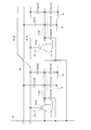
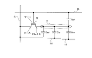
- FIG. 1 is a circuit diagram showing a configuration of a pixel formation portion in the present embodiment.
- FIG. 1 shows components corresponding to one pixel formation portion.
- a pixel TFT 10 having a gate electrode connected to a gate bus electrode GL passing through a corresponding intersection and a source electrode connected to a source bus electrode SL passing through the intersection.
- the pixel electrode 11 connected to the drain electrode of the pixel TFT 10, the common electrode (counter electrode) 18 and the auxiliary capacitance electrode 19 that are commonly provided in the plurality of pixel forming portions, the pixel electrode 11 and the common electrode 18, a pixel capacitor (liquid crystal capacitor) Clc formed by 18, an auxiliary capacitor Ccs formed by the pixel electrode 11 and the auxiliary capacitor electrode 19, a source bus electrode SL and a drain electrode (pixel electrode 11) of the pixel TFT 10.
- the pixel forming portion in the present embodiment is formed by the capacitor forming electrode EL and the drain electrode (pixel electrode 11) of the pixel TFT 10 in addition to the components in the conventional general liquid crystal display device.
- An additional capacitor Ca is provided.
- the additional capacitance Ca and the gate-drain capacitance Cgd have the same capacitance value.
- the first capacitance is realized by the gate-drain capacitance Cgd
- the second capacitance is realized by the additional capacitance.
- FIG. 3 is a signal waveform diagram for explaining the driving method in the present embodiment.
- the high-level voltage (gate-on voltage) of the scanning signal G (k) is Vgh
- the low-level voltage (gate-off voltage) of the scanning signal G (k) is Vgl.
- the capacitance forming electrode drive signal E (k) is changed from the high level to the low level immediately before the corresponding scanning signal G (k) rises (at the time when the low level changes to the high level).
- the voltage on the high level side of the capacitance forming electrode drive signal E (k) is the gate-on voltage Vgh, and the voltage on the low level side of the capacitance forming electrode drive signal E (k) is the gate-off voltage Vgl.
- ⁇ Vd2 (Vgl ⁇ Vgh) ⁇ Ca / (Clc + Ccs + Csd + Cgd + Ca) ... (3)
- the timing at which the capacitance forming electrode drive signal E (k) is changed from the low level to the high level after the scanning signal G (k) rises is the same as when the scanning signal G (k) falls, or The time must be later than the time when the scanning signal G (k) falls.
- the reason for this is as follows. If the capacitance forming electrode drive signal E (k) is changed from the low level to the high level before the time point when the scanning signal G (k) falls, the pixel TFT 10 is not turned off. Therefore, the above-described voltage fluctuation ⁇ Vd2 does not occur in the pixel electrode 11. For this reason, the influence of the feedthrough voltage ⁇ Vd1 generated immediately after the falling point t2 of the scanning signal G (1) appears as, for example, flicker.
- the timing at which the capacitance forming electrode drive signal E (k) is changed from the high level to the low level so as to reduce the influence of the voltage fluctuation ⁇ Vd3 is immediately before the time when the scanning signal G (k) rises, or
- the scanning signal G (k) is preferably set to a point in time during which the scanning signal G (k) is at a high level.
- the capacitance forming electrode drive signal E (k) changes from the high level to the low level at a time t0 that is just a short period T1 before the time t1 when the scanning signal G (k) rises. ing.
- the display unit 100 of the liquid crystal display device is provided with the capacitance forming electrodes EL1 to ELi so as to correspond to the gate bus electrodes GL1 to GLi on a one-to-one basis.
- the additional capacitance Ca described above is formed between the capacitance forming electrodes EL1 to ELi and the pixel electrode (drain electrode of the pixel TFT 10) 11 in each pixel forming portion.
- the capacitance forming electrode drive signals E (1) to E (i) rise. It is done.
- the capacitance value of the additional capacitor Ca is equal to the capacitance value of the gate-drain capacitance Cgd. For this reason, immediately after the rise of the capacitance forming electrode drive signals E (1) to E (i), the fluctuation of the potential generated in the pixel electrode 11 due to the fall of the scanning signals G (1) to G (i). The potential of the pixel electrode 11 varies so as to cancel out. As a result, there is no difference in the liquid crystal applied voltage when a positive voltage is applied to the pixel electrode 11 and when a negative voltage is applied to the pixel electrode 11. As a result, the occurrence of flicker due to the feedthrough voltage is suppressed. Unlike the inventions disclosed in Japanese Patent Laid-Open Nos.
- the potential of the pixel electrode 11 is affected by the voltage fluctuation ⁇ Vd3.
- the potential of the pixel electrode 11 is affected by the voltage fluctuation ⁇ Vd1.
- the period indicated by the symbol T3 is a period that is not affected by the voltage fluctuation ⁇ Vd1 or the voltage fluctuation ⁇ Vd3.
- the length of T1 and T2 is sufficiently shorter than the length of T3 (for example, the length of T1 and T2 is set to a length within one horizontal scanning period), which is caused by the feedthrough voltage. The occurrence of flicker is effectively suppressed.
- the gate bus electrodes GL1 to GLi are arranged so as to extend from the gate driver 400 disposed on the left side of the display unit 100 to the display unit 100 in the left-right direction in FIG.
- the electrodes EL1 to ELi are arranged so as to extend from the capacitance forming electrode driver 500 disposed on the right side of the display unit 100 to the display unit 100, but the present invention is not limited to this.
- Both the gate bus electrodes GL1 to GLi and the capacitance forming electrodes EL1 to ELi may be disposed so as to extend from the driver disposed on one side of the display unit 100 to the display unit 100.
- both the gate bus electrodes GL1 to GLi and the capacitance forming electrodes EL1 to ELi may be arranged so as to extend from the drivers arranged on both sides of the display unit 100 to the display unit 100.
- Second Embodiment> ⁇ 2.1 Configuration of Pixel Forming Unit>
- a VA mode Vertical alignment mode
- pixel division method a method of dividing one pixel into two subpixels.
- the overall configuration and operation of the liquid crystal display device are substantially the same as those in the first embodiment, and a description thereof will be omitted. However, since one pixel is divided into two sub-pixels, the number of source bus electrodes is doubled as compared to the first embodiment.
- FIG. 4 is a circuit diagram showing a configuration of a pixel formation unit in the second embodiment of the present invention.
- one pixel formation portion is disposed on the left side in FIG. 4 (hereinafter referred to as “first subpixel formation portion”) and on the right side in FIG.
- a sub-pixel forming portion (hereinafter referred to as “second sub-pixel forming portion”).
- (a) is added to the code
- (b) is added to the code
- each capacity and the capacity value of each capacity are denoted by the same reference numerals.
- Each sub-pixel forming unit is configured in the same manner as the pixel forming unit in the first embodiment. Therefore, the additional capacitor Ca (a) and the gate-drain capacitor Cgd (a) have the same capacitance value in the first subpixel formation portion, and the additional capacitor Ca (b) in the second subpixel formation portion. And the gate-drain capacitance Cgd (b) have the same capacitance value.
- the source electrode of the pixel TFT 10 (a) in the first sub-pixel formation portion and the source electrode of the pixel TFT 10 (b) in the second sub-pixel formation portion are different from each other. , SL (b). Therefore, by applying different video signals from the source driver 300 to the source bus electrode SL (a) and the source bus electrode SL (b), the pixel electrode 11 (a) and the second subpixel in the first subpixel formation unit are applied. Different voltages can be applied to the pixel electrode 11 (b) in the formation portion.
- the gate electrode of the pixel TFT 10 (a) in the first subpixel formation portion and the gate electrode of the pixel TFT 10 (b) in the second subpixel formation portion are connected to the same gate bus electrode GL.
- An additional capacitor having one end connected to the other end of the additional capacitor Ca (a) having one end connected to the pixel electrode 11 (a) in the first subpixel forming portion and a pixel electrode 11 (b) having the one end connected to the pixel electrode 11 (b) in the second subpixel forming portion.
- the other end of Ca (b) is connected to the same capacitance forming electrode EL.
- the second video signal electrode is realized by the source bus electrode SL (b) connected to the source electrode of the pixel TFT 10 (b) in the second subpixel formation portion.
- the gate bus electrodes GL1 to GLi and the capacitance forming electrodes EL1 to ELi are driven in the same manner as in the first embodiment. That is, the waveform of the scanning signal and the waveform of the capacitor forming electrode drive signal are as shown in FIG. 3 as in the first embodiment.
- the pixel electrode 11 (a) in the first sub-pixel formation portion has a voltage variation ⁇ Vd1a expressed by the following equation (5), and the second sub-pixel formation portion in the second sub-pixel formation portion.
- a voltage fluctuation ⁇ Vd1b expressed by the following equation (6) occurs.
- ⁇ Vd1a (Vgh ⁇ Vgl) ⁇ Cgd (a) / (Clc (a) + Ccs (a) + Csd (a) + Ca (a))
- ⁇ Vd1b (Vgh ⁇ Vgl) ⁇ Cgd (b) / (Clc (b) + Ccs (b) + Csd (b) + Ca (b)) (6)
- ⁇ Vd2a (Vgl ⁇ Vgh) ⁇ Ca (a) / (Clc (a) + Ccs (a) + Csd (a) + Ca (a)) (7)
- ⁇ Vd2b (Vgl ⁇ Vgh) ⁇ Ca (b) / (Clc (b) + Ccs (b) + Csd (b) + Ca (b)) (8)
- the pixel electrode 11 (a) has a voltage variation ⁇ Vd3a expressed by the following equation (9), and the pixel electrode 11 (b) Then, the voltage fluctuation ⁇ Vd3b expressed by the following equation (10) occurs.
- ⁇ Vd3a (Vgh ⁇ Vgl) ⁇ Ca (a) / (Clc (a) + Ccs (a) + Csd (a) + Ca (a)) (9)
- ⁇ Vd3b (Vgh ⁇ Vgl) ⁇ Ca (b) / (Clc (b) + Ccs (b) + Csd (b) + Cgd (b) + Ca (b)) (10)
- the timing at which the capacitance forming electrode drive signal is changed from the high level to the low level is set so that the influence of the voltage fluctuations ⁇ Vd3a and ⁇ Vd3b is reduced. It is preferable that the time point is just before the rising point or during a period in which the scanning signal is at a high level.
- the first sub-pixel forming unit that forms one of the divided pixels and the divided pixels
- the following operation is performed in both of the second sub-pixel forming portions that form the other of the pixels.
- the potential of the pixel electrode fluctuates as in the conventional case.
- the rise of the capacitance forming electrode drive signal causes the potential of the pixel electrode to fluctuate so that the fluctuation of the potential generated in the pixel electrode immediately after the fall of the scanning signal is canceled.
- the liquid crystal applied voltage is changed when a positive voltage is applied to the pixel electrode and when a negative voltage is applied to the pixel electrode. There is no difference. As described above, the occurrence of flicker due to the feedthrough voltage is suppressed in the liquid crystal display device adopting the pixel division method.
- FIG. 5 is a circuit diagram showing a configuration of the pixel formation portion in the first modification of the second embodiment.
- the source electrode of the pixel TFT 10 (a) in the first subpixel formation unit and the source electrode of the pixel TFT 10 (b) in the second subpixel formation unit are: The same source bus electrode SL is connected.
- the gate electrode of the pixel TFT 10 (a) in the first sub-pixel formation portion and the gate electrode of the pixel TFT 10 (b) in the second sub-pixel formation portion are different from each other.
- the electrodes GL (a) and GL (b) are connected.
- the number of source bus electrodes is the same as that in the first embodiment, but the number of gate bus electrodes is twice that in the first embodiment.
- the gate driver 400 operates the gate bus electrode GL (a) so that the pixel TFT 10 (a) in the first subpixel formation unit and the pixel TFT10 (b) in the second subpixel formation unit are turned on in different periods.
- GL (b) are driven, different voltages can be applied to the pixel electrode 11 (a) in the first subpixel formation portion and the pixel electrode 11 (b) in the second subpixel formation portion.
- the additional capacitance Ca (a) and the gate-drain capacitance Cgd (a) have the same capacitance value in the first subpixel formation portion, and the additional capacitance in the second subpixel formation portion.
- the capacitance values of Ca (b) and gate-drain capacitance Cgd (b) are equal.
- the second scanning signal electrode is realized by the gate bus electrode GL (b) connected to the gate electrode of the pixel TFT 10 (b) in the second subpixel formation portion.
- FIG. 6 is a signal waveform diagram for explaining a driving method in the present modification.
- FIG. 6 shows a scanning signal Ga for controlling the state of the pixel TFT 10 (a) in the first sub-pixel formation portion when focusing on one row, and the state of the pixel TFT 10 (b) in the second sub-pixel formation portion.
- the waveforms of the scanning signal Gb for controlling the voltage and the electrode drive signal E for forming the capacitance are shown.
- the scanning signal Ga is set to the high level during the period from the time point t1 to the time point t2
- the scanning signal Gb is set to the high level during the period from the time point t3 to the time point t4.
- the capacitance forming electrode drive signal E changes from a high level to a low level at a time t0 immediately before the time t1 when the scanning signal Ga rises, and goes low at a time t5 after the time t4 when the scanning signal Gb falls. Driven to change from level to high level.
- the voltage fluctuation ⁇ Vd1a expressed by the above equation (5) occurs in the pixel electrode 11 (a) in the first subpixel formation portion, and the scanning signal Gb is Immediately after the falling time t4, the voltage fluctuation ⁇ Vd1b represented by the above equation (6) occurs in the pixel electrode 11 (b) in the second subpixel formation portion. Further, immediately after the time point t5 when the capacitance forming electrode drive signal E changes from the low level to the high level, the voltage fluctuation ⁇ Vd2a represented by the above equation (7) is generated in the pixel electrode 11 (a) in the first subpixel formation portion.
- the voltage fluctuation ⁇ Vd2b represented by the above equation (8) occurs in the pixel electrode 11 (b) in the second subpixel formation portion.
- the capacitance forming electrode drive signal E changes from the low level to the high level.
- the potential of the pixel electrode 11 (a) in the first subpixel formation unit and the potential of the pixel electrode 11 (b) in the second subpixel formation unit so that the voltage fluctuations ⁇ Vd1a and ⁇ Vd1b are canceled.
- the potential fluctuates.
- the potential of the pixel electrode 11 (a) in the first subpixel formation portion is affected by the voltage fluctuation ⁇ Vd3a expressed by the above equation (9) during the period indicated by reference numeral T1 in FIG.
- the potential of the pixel electrode 11 (b) in the second subpixel formation portion is affected by the voltage fluctuation ⁇ Vd3b expressed by the above equation (10).
- the potential of the pixel electrode 11 (a) in the first subpixel formation portion is affected by the voltage fluctuation ⁇ Vd1a, and during the period indicated by reference numeral T4 in FIG.
- the potential of the pixel electrode 11 (b) in the two subpixel formation portion is affected by the voltage fluctuation ⁇ Vd1b.
- the period indicated by reference numeral T5 in FIG. 6 is a period that is not affected by the voltage fluctuations ⁇ Vd1a, ⁇ Vd1b, ⁇ Vd3a, and ⁇ Vd3b. From the above, it is possible to suppress the occurrence of flicker due to the feedthrough voltage by making the length of T1 to T4 sufficiently shorter than the length of T5.
- FIG. 7 is a circuit diagram showing a configuration of a pixel formation portion in a second modification of the second embodiment.
- the source electrode of the pixel TFT 10 (a) in the first subpixel formation unit and the source electrode of the pixel TFT 10 (b) in the second subpixel formation unit are: The same source bus electrode SL is connected.
- the gate electrode of the pixel TFT 10 (a) in the first subpixel formation portion and the gate electrode of the pixel TFT 10 (b) in the second subpixel formation portion are connected to the same gate bus electrode GL.
- the number of source bus electrodes and the number of gate bus electrodes are the same as those in the first embodiment.
- the additional capacitor Ca (a) and the gate-drain capacitance Cgd (a) have the same capacitance value in the first subpixel formation portion, and in the second subpixel formation portion, The additional capacitance Ca (b) and the gate-drain capacitance Cgd (b) have the same capacitance value.
- the capacitance values of the source-drain capacitance Cgd (a), the auxiliary capacitance Ccs (a), and the pixel capacitance Clc (a) in the first subpixel formation portion are respectively in the second subpixel formation portion.
- the source-drain capacitance Cgd (b), the auxiliary capacitance Ccs (b), and the pixel capacitance Clc (b) have different values.
- the capacitance value of at least one of the source-drain capacitance, the auxiliary capacitance, and the pixel capacitance is different between the first subpixel formation portion and the second subpixel formation portion.
- the third capacitor is realized by at least one of the source-drain capacitor, the auxiliary capacitor, and the pixel capacitor.
- the induced voltage ⁇ V1 generated at the pixel electrode 11 due to the voltage change of the video signal is expressed by the following formula ( 11).
- ⁇ V1 Vs ⁇ Csd / (Clc + Ccs + Csd + Cgd + Ca) (11)
- the common electrode driving signal for driving the common electrode 18 a driving method is employed in which the polarity of the voltage is inverted every predetermined period with a predetermined potential as a reference, and the voltage amplitude for the common electrode driving signal is Vc.
- the induced voltage ⁇ V1, ⁇ V2 is different between the first subpixel formation portion and the second subpixel formation portion.
- the scanning signal and the capacitance formation electrode are applied. Variations in the potentials of the pixel electrodes 11 (a) and 11 (b) based on the change in voltage of the drive signal are the same as in the second embodiment. For this reason, also in this modification, generation
- FIG. 8 is a signal waveform diagram for explaining the driving method in the present embodiment.
- the gate bus electrodes are driven in the same manner as in the first embodiment (same as in the prior art) so that active scanning signals are sequentially given one by one.
- the capacitor forming electrodes unlike the first embodiment, the capacitor forming electrode driving signals having the same waveform are provided n by n.
- the capacitance forming electrode driver 500 starts from the time when all of the scanning signals applied to the gate bus electrodes corresponding to the n capacitance forming electrodes to which the capacitance forming electrode driving signal having the same waveform is applied fall. Further, the capacitance forming electrode drive signal applied to the n capacitance forming electrodes is changed from the low level to the high level.
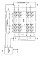
- FIG. 9 is a diagram showing a configuration example of the capacitance forming electrode in the present embodiment.
- one electrode hereinafter referred to as “capacitor forming trunk electrode” extending from the capacitor forming electrode driver 500 in a region between the display unit 100 and the capacitor forming electrode driver 500 is provided. It is connected to four capacitance forming electrodes.
- the capacitance forming electrodes EL1 to ELi provided in the display unit 100 are grouped by four in the region between the display unit 100 and the capacitance forming electrode driver 500.
- the capacitance forming electrodes EL1 to EL4 corresponding to the gate bus electrodes in the first to fourth rows are grouped and connected to the capacitance forming trunk electrode EG1.
- the capacitance forming electrodes EL13 to EL16 corresponding to the gate bus electrodes in the 13th to 16th rows are grouped and connected to the capacitance forming trunk electrode EG4.
- the capacitance forming electrode driver 500 drives the capacitance forming trunk electrode EG1
- the capacitance forming electrodes EL1 to EL4 are supplied with the capacitance forming electrode driving signals having the same waveform.
- the electrode driver 500 drives the capacitance forming trunk electrode EG4
- the capacitance forming electrodes EL13 to EL16 are supplied with the capacitance forming electrode drive signal having the same waveform.
- the period is affected by the potential fluctuation ⁇ Vd1 at the pixel electrode due to the fall of the scanning signal and the potential fluctuation ⁇ Vd3 at the pixel electrode due to the rise of the capacitance forming electrode drive signal.
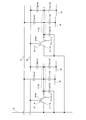
- FIG. 10 is a circuit diagram showing a configuration of a pixel formation portion in a modification of the third embodiment.
- FIG. 10 shows components corresponding to four pixel formation portions arranged continuously in the extending direction of the source bus electrode SL.
- one capacitor forming electrode is provided for every two gate bus electrodes arranged continuously in the extending direction of the source bus electrode SL.
- Each capacitance forming electrode is disposed in a region between two pixel formation portions that are continuously disposed in the extending direction of the source bus electrode SL.
- the capacitance forming electrode EL1 is disposed in a region between the pixel forming portion corresponding to the gate bus electrode GL1 and the pixel forming portion corresponding to the gate bus electrode GL2. Further, an additional capacitance Ca is formed between the pixel electrode 11 in the pixel formation portion corresponding to the gate bus electrode GL1 and the capacitance formation electrode EL1, and the pixel electrode 11 in the pixel formation portion corresponding to the gate bus electrode GL2 An additional capacitor Ca is also formed between the capacitor forming electrode EL1.
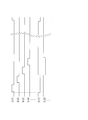
- FIG. 11 is a signal waveform diagram for explaining a driving method in the present modification.
- the capacitor forming electrode driver 500 is operated after both of the scanning signals applied to the two scanning signal electrodes corresponding to the capacitor forming electrode fall. Then, the capacitance forming electrode drive signal applied to the capacitance forming electrode is changed from the low level to the high level. Further, the capacitance forming electrode driver 500 applies the capacitance forming electrode to the capacitance forming electrode immediately before one of the scanning signals applied to the two scanning signal electrodes corresponding to the capacitance forming electrode rises. The capacitance-forming electrode drive signal that has been set is changed from a high level to a low level.
- the capacitance forming electrodes are shared by the odd-numbered rows and the even-numbered rows. For this reason, it is possible to suppress the occurrence of flicker due to the feedthrough voltage while suppressing the decrease in the aperture ratio due to the provision of the capacitance forming electrode.
- Pixel TFT type> In each of the above embodiments, an N-channel TFT is adopted as the pixel TFT. However, the present invention is not limited to this, and the present invention is also applied to a case where a P-channel TFT is adopted as the pixel TFT. Can be applied.
- the capacitance value of the additional capacitor Ca and the capacitance value of the gate-drain capacitor Cgd are equal.
- the present invention is not limited to this, and the capacitance value of the additional capacitor Ca is set between the gate and drain.
- the capacitance value of the capacitance Cgd may be M times (M is a positive number).
- the capacitance forming electrode driver 500 sets the amplitude of the capacitance forming electrode driving signal E (k) to “(Vgh ⁇ Vgl) / 2”.
- the capacitance value of the additional capacitor Ca is set to M times the capacitance value of the gate-drain capacitance Cgd (M is a positive number), and the amplitude of the capacitance forming electrode drive signal E (k) is set as the scanning signal.
- the flicker caused by the feedthrough voltage can also be suppressed by setting the amplitude of G (k) to (1 / M) times.
- the amplitude of the capacitance forming electrode drive signal E (k) is set to the scanning signal G (k ) Is close to (1 / M) times the amplitude, the flicker caused by the feedthrough voltage cannot be completely suppressed, but the occurrence of the flicker can be suppressed. It becomes.
- an auxiliary capacitor Ccs is often provided in parallel with a pixel capacitor (liquid crystal capacitor) Clc as shown in FIG. 13 so that the voltage to be applied to the liquid crystal is reliably maintained.
- a liquid crystal display device that does not include the auxiliary capacitor Ccs. Therefore, in the following, a case where a configuration that does not include the auxiliary capacitor Ccs is applied to the first embodiment will be described as an example.
- FIG. 12 is a circuit diagram showing a configuration of a pixel formation portion in this modification. Unlike the configuration in the first embodiment shown in FIG. 1, the auxiliary capacitance electrode 19 and the auxiliary capacitance Ccs are not provided in the pixel formation portion.
- the fluctuation of the potential of the pixel electrode 11 in the present modification will be described. Although the description will be given focusing on the first row, the same operation is performed in all rows.
- ⁇ Vd1c (Vgh ⁇ Vgl) ⁇ Cgd / (Clc + Csd + Cgd + Ca) (14)
- the capacitance forming electrode drive signal E (1) changes from the low level to the high level.
- the pixel electrode 11 has a voltage fluctuation ⁇ Vd2c expressed by the following equation (15).
- ⁇ Vd2c (Vgl ⁇ Vgh) ⁇ Ca / (Clc + Csd + Cgd + Ca) ...
Landscapes
- Engineering & Computer Science (AREA)
- Chemical & Material Sciences (AREA)
- Crystallography & Structural Chemistry (AREA)
- Physics & Mathematics (AREA)
- Computer Hardware Design (AREA)
- General Physics & Mathematics (AREA)
- Theoretical Computer Science (AREA)
- Power Engineering (AREA)
- Control Of Indicators Other Than Cathode Ray Tubes (AREA)
- Liquid Crystal (AREA)
Abstract
本発明は、フィードスルー電圧に起因するフリッカーの発生を簡易な構成で抑止することのできる表示装置を提供することを目的とする。 画素形成部内の画素電極(11)との間に追加容量(Ca)が形成されるように容量形成用電極(EL)が設けられ、その追加容量(Ca)の容量値はゲート-ドレイン間容量(Cgd)の容量値と等しくされる。走査信号電極(GL)に印加されている走査信号が立ち下げられた時点以降に、容量形成用電極ドライバ(500)は、当該走査信号電極(GL)に対応する容量形成用電極(EL)に印加されている容量形成用電極駆動信号を立ち上げる。
Description
本発明は、薄膜トランジスタ等のスイッチング素子を用いたアクティブマトリクス型の表示装置およびその駆動方法に関する。
従来より、スイッチング素子としてTFT(Thin Film Transistor:薄膜トランジスタ)を備えるアクティブマトリクス型の液晶表示装置が知られている。この液晶表示装置には、主要な構成要素として、マトリクス状に配置された複数個の画素形成部からなる表示部としての液晶パネルとその駆動回路とが設けられている。液晶パネルには、複数本のソースバス電極(映像信号線)と複数本のゲートバス電極(走査信号線)とが互いに交差するように格子状に形成されており、さらに、ゲートバス電極と1対1で対応するように補助容量電極が形成されている。複数本のソースバス電極と複数本のゲートバス電極との交差点のそれぞれには1つの画素形成部が対応している。また、液晶パネルは、マトリクス状に配置された上記複数個の画素形成部に共通的に設けられ、各画素形成部に含まれる画素電極と液晶を挟んで対向するように配置された共通電極を備えている。
図13は、上述した従来の液晶表示装置における画素形成部の構成を示す回路図である。図13に示すように、各画素形成部には、対応する交差点を通過するゲートバス電極GLにゲート電極が接続されるとともに当該交差点を通過するソースバス電極SLにソース電極が接続されたTFT(以下「画素TFT」という。)10と、画素TFT10のドレイン電極に接続された画素電極11と、上記複数個の画素形成部に共通的に設けられた共通電極(対向電極)18および補助容量電極19と、画素電極11と共通電極18とによって形成される画素容量(液晶容量)Clcと、画素電極11と補助容量電極19とによって形成される補助容量Ccsと、ソースバス電極SLと画素TFT10のドレイン電極(画素電極11)とによって形成される容量(以下「ソース-ドレイン間容量」という。)Csdと、ゲートバス電極GLと画素TFT10のドレイン電極(画素電極11)とによって形成される容量(以下「ゲート-ドレイン間容量」という。)Cgdとが含まれている。なお、以下においては、上記容量Clc,Ccs,Csd,Cgdの容量値についても、同じ符号“Clc”,“Ccs”,“Csd”,“Cgd”でそれぞれ示す。
上述のように、各画素形成部にはゲート-ドレイン間容量Cgdが形成されている。このため、図14Aに示すような波形の映像信号Sがソースバス電極SLに印加されていると、図14Bに示すように走査信号Gの電圧がゲートオン電圧Vghからゲートオフ電圧Vglへと立ち下がる時に、図14Cに示すように画素電極の電位(画素電位)Vdにはゲート-ドレイン間容量Cgdに起因する電圧変動ΔVdが生じる。この電圧変動ΔVdは、次式(1)で表される。
ΔVd=(Vgh-Vgl)×Cgd/(Clc+Ccs+Csd+Cgd)
・・・(1)
なお、上記電圧変動ΔVdは「フィードスルー電圧」,「引き込み電圧」等と呼ばれている。
ΔVd=(Vgh-Vgl)×Cgd/(Clc+Ccs+Csd+Cgd)
・・・(1)
なお、上記電圧変動ΔVdは「フィードスルー電圧」,「引き込み電圧」等と呼ばれている。
ところで、上述の電圧変動ΔVdは、(共通電極18の電位Vcomを基準として)画素電極11に正極性の電圧が印加されるときには、図14Cで符号91で示す部分から把握されるように、液晶印加電圧を所望の電圧よりも小さくするように作用する。一方、画素電極11に負極性の電圧が印加されるときには、図14Cで符号92で示す部分から把握されるように、上述の電圧変動ΔVdは、液晶印加電圧を所望の電圧よりも大きくするように作用する。このため、画素電極11に正極性の電圧が印加されるときと画素電極11に負極性の電圧が印加されるときとで液晶印加電圧が異なる。その結果、画面にフリッカー(ちらつき)が生じる。
そこで、日本の特開平4-5633号公報および日本の特開平4-14091号公報には、1つの画素形成部内にNチャンネル型のTFTとPチャンネル型のTFTとを備えることによって、フィードスルー電圧(引き込み電圧)に起因するフリッカーの発生を抑止する発明が開示されている。日本の特開平4-5633号公報に開示された表示装置では、各画素形成部内でNチャンネル型のTFTとPチャンネル型のTFTとを交互にオン状態にすることによって、液晶印加電圧の極性に関わらず電圧変動ΔVdが共通電極の電位側へ生じるようにされている。日本の特開平4-14091号公報に開示された表示装置では、Nチャンネル型のTFTとPチャンネル型のTFTとを同時にオン状態にしてNチャンネル型のTFTおよびPチャンネル型のTFTの双方を介して映像信号の書き込みが行われるようにすることによって、電圧変動ΔVdが0になるようにされている。
ところが、日本の特開平4-5633号公報および日本の特開平4-14091号公報に開示された発明によると、Nチャンネル型のTFTとPチャンネル型のTFTとを各画素形成部に備える必要がある。このため、画素回路の構成が複雑化し、高コストとなる。
そこで本発明は、フィードスルー電圧(引き込み電圧)に起因するフリッカーの発生を簡易な構成で抑止することのできる表示装置を提供することを目的とする。
本発明の第1の局面は、複数本の映像信号電極と、前記複数本の映像信号電極と交差する複数本の走査信号電極と、前記複数本の映像信号電極と前記複数本の走査信号電極との交差点にそれぞれ対応してマトリクス状に配置された複数個の画素形成部とを有するアクティブマトリクス型の表示装置であって、
前記複数本の映像信号電極と交差する複数本の容量形成用電極と、
表示すべき画像を表す映像信号を前記複数本の映像信号電極に印加する映像信号電極駆動部と、
前記複数本の走査信号電極に走査信号を印加することによって前記複数本の走査信号電極を選択的に駆動する走査信号電極駆動部と、
前記複数本の容量形成用電極を駆動する容量形成用電極駆動部と
を備え、
前記複数本の容量形成用電極のそれぞれは、前記複数本の走査信号電極のうちの少なくとも1本と対応するように設けられ、
各画素形成部は、対応する交差点を通過する走査信号電極である対応走査信号電極に印加されている走査信号が第1レベルであるときにオン状態となり当該走査信号が第2レベルであるときにオフ状態となるスイッチング素子と、対応する交差点を通過する映像信号電極に前記スイッチング素子を介して接続され前記対応走査信号電極との間に第1容量が形成されるように配置された画素電極と、前記対応走査信号電極に対応する容量形成用電極と前記画素電極とによって形成される第2容量とを含み、
前記容量形成用電極駆動部は、各走査信号電極に印加されている走査信号が前記第1レベルから前記第2レベルに変化した時点以降に、当該各走査信号電極に対応する容量形成用電極への印加電圧を、前記走査信号についての前記第1レベルから前記第2レベルへの変化とは逆の方向に変化させることを特徴とする。
前記複数本の映像信号電極と交差する複数本の容量形成用電極と、
表示すべき画像を表す映像信号を前記複数本の映像信号電極に印加する映像信号電極駆動部と、
前記複数本の走査信号電極に走査信号を印加することによって前記複数本の走査信号電極を選択的に駆動する走査信号電極駆動部と、
前記複数本の容量形成用電極を駆動する容量形成用電極駆動部と
を備え、
前記複数本の容量形成用電極のそれぞれは、前記複数本の走査信号電極のうちの少なくとも1本と対応するように設けられ、
各画素形成部は、対応する交差点を通過する走査信号電極である対応走査信号電極に印加されている走査信号が第1レベルであるときにオン状態となり当該走査信号が第2レベルであるときにオフ状態となるスイッチング素子と、対応する交差点を通過する映像信号電極に前記スイッチング素子を介して接続され前記対応走査信号電極との間に第1容量が形成されるように配置された画素電極と、前記対応走査信号電極に対応する容量形成用電極と前記画素電極とによって形成される第2容量とを含み、
前記容量形成用電極駆動部は、各走査信号電極に印加されている走査信号が前記第1レベルから前記第2レベルに変化した時点以降に、当該各走査信号電極に対応する容量形成用電極への印加電圧を、前記走査信号についての前記第1レベルから前記第2レベルへの変化とは逆の方向に変化させることを特徴とする。
本発明の第2の局面は、本発明の第1の局面において、
前記第2容量の容量値は、前記第1容量の容量値と等しくされ、
前記容量形成用電極駆動部は、各走査信号電極に印加されている走査信号が前記第1レベルから前記第2レベルに変化した時点以降に、当該各走査信号電極に対応する容量形成用電極への印加電圧を前記第2レベルから前記第1レベルに変化させることを特徴とする。
前記第2容量の容量値は、前記第1容量の容量値と等しくされ、
前記容量形成用電極駆動部は、各走査信号電極に印加されている走査信号が前記第1レベルから前記第2レベルに変化した時点以降に、当該各走査信号電極に対応する容量形成用電極への印加電圧を前記第2レベルから前記第1レベルに変化させることを特徴とする。
本発明の第3の局面は、本発明の第1の局面において、
前記第2容量の容量値は、前記第1容量の容量値よりも大きくされ、
前記容量形成用電極駆動部は、前記容量形成用電極への印加電圧の振幅が前記走査信号の振幅よりも小さくなるように前記容量形成用電極を駆動することを特徴とする。
前記第2容量の容量値は、前記第1容量の容量値よりも大きくされ、
前記容量形成用電極駆動部は、前記容量形成用電極への印加電圧の振幅が前記走査信号の振幅よりも小さくなるように前記容量形成用電極を駆動することを特徴とする。
本発明の第4の局面は、本発明の第1の局面において、
前記第2容量の容量値は、前記第1容量の容量値よりも小さくされ、
前記容量形成用電極駆動部は、前記容量形成用電極への印加電圧の振幅が前記走査信号の振幅よりも大きくなるように前記容量形成用電極を駆動することを特徴とする。
前記第2容量の容量値は、前記第1容量の容量値よりも小さくされ、
前記容量形成用電極駆動部は、前記容量形成用電極への印加電圧の振幅が前記走査信号の振幅よりも大きくなるように前記容量形成用電極を駆動することを特徴とする。
本発明の第5の局面は、本発明の第1の局面において、
前記第2容量の容量値は、前記第1容量の容量値のM倍(Mは正の数)とされ、
前記容量形成用電極駆動部は、前記容量形成用電極への印加電圧の振幅が前記走査信号の振幅のM分の1となるように前記容量形成用電極を駆動することを特徴とする。
前記第2容量の容量値は、前記第1容量の容量値のM倍(Mは正の数)とされ、
前記容量形成用電極駆動部は、前記容量形成用電極への印加電圧の振幅が前記走査信号の振幅のM分の1となるように前記容量形成用電極を駆動することを特徴とする。
本発明の第6の局面は、本発明の第1の局面において、
各画素形成部は、それぞれが前記スイッチング素子と前記画素電極と前記第2容量とを含む第1副画素形成部と第2副画素形成部とからなることを特徴とする。
各画素形成部は、それぞれが前記スイッチング素子と前記画素電極と前記第2容量とを含む第1副画素形成部と第2副画素形成部とからなることを特徴とする。
本発明の第7の局面は、本発明の第6の局面において、
前記複数本の映像信号電極の本数に等しい複数本の第2映像信号電極を更に有し、
前記映像信号電極駆動部は、前記映像信号を更に前記複数本の第2映像信号電極に印加し、
前記第1副画素形成部に含まれる画素電極は、前記スイッチング素子を介して前記映像信号電極に接続され、
前記第2副画素形成部に含まれる画素電極は、前記スイッチング素子を介して前記第2映像信号電極に接続されていることを特徴とする。
前記複数本の映像信号電極の本数に等しい複数本の第2映像信号電極を更に有し、
前記映像信号電極駆動部は、前記映像信号を更に前記複数本の第2映像信号電極に印加し、
前記第1副画素形成部に含まれる画素電極は、前記スイッチング素子を介して前記映像信号電極に接続され、
前記第2副画素形成部に含まれる画素電極は、前記スイッチング素子を介して前記第2映像信号電極に接続されていることを特徴とする。
本発明の第8の局面は、本発明の第6の局面において、
前記複数本の走査信号電極の本数に等しい複数本の第2走査信号電極を更に有し、
前記走査信号電極駆動部は、前記走査信号を更に前記複数本の第2走査信号電極に印加することによって、前記走査信号電極と前記第2走査信号電極とが交互に選択されるように前記複数本の走査信号電極と前記複数本の第2走査信号電極とを選択的に駆動し、
前記第2副画素形成部において、
前記スイッチング素子は、前記対応走査信号電極に代えて対応する交差点を通過する第2走査信号電極である対応第2走査信号電極に印加されている走査信号が第1レベルであるときにオン状態となり当該走査信号が第2レベルであるときにオフ状態となり、
前記画素電極は、前記対応走査信号電極に代えて前記対応第2走査信号電極との間に第1容量が形成されるように配置され、
前記容量形成用電極駆動部は、各容量形成用電極に対応する走査信号電極に印加されている走査信号および当該各容量形成用電極に対応する第2走査信号電極に印加されている走査信号の双方について前記第1レベルから前記第2レベルへの変化が終了した時点以降に、当該各容量形成用電極への印加電圧を、前記双方の走査信号についての前記第1レベルから前記第2レベルへの変化とは逆の方向に変化させることを特徴とする。
前記複数本の走査信号電極の本数に等しい複数本の第2走査信号電極を更に有し、
前記走査信号電極駆動部は、前記走査信号を更に前記複数本の第2走査信号電極に印加することによって、前記走査信号電極と前記第2走査信号電極とが交互に選択されるように前記複数本の走査信号電極と前記複数本の第2走査信号電極とを選択的に駆動し、
前記第2副画素形成部において、
前記スイッチング素子は、前記対応走査信号電極に代えて対応する交差点を通過する第2走査信号電極である対応第2走査信号電極に印加されている走査信号が第1レベルであるときにオン状態となり当該走査信号が第2レベルであるときにオフ状態となり、
前記画素電極は、前記対応走査信号電極に代えて前記対応第2走査信号電極との間に第1容量が形成されるように配置され、
前記容量形成用電極駆動部は、各容量形成用電極に対応する走査信号電極に印加されている走査信号および当該各容量形成用電極に対応する第2走査信号電極に印加されている走査信号の双方について前記第1レベルから前記第2レベルへの変化が終了した時点以降に、当該各容量形成用電極への印加電圧を、前記双方の走査信号についての前記第1レベルから前記第2レベルへの変化とは逆の方向に変化させることを特徴とする。
本発明の第9の局面は、本発明の第6の局面において、
各画素形成部に含まれる画素電極は、前記対応走査信号電極以外の電極との間に第3容量が形成されるように配置され、
前記第3容量の容量値が前記第1副画素形成部と前記第2副画素形成部とで異なることを特徴とする。
各画素形成部に含まれる画素電極は、前記対応走査信号電極以外の電極との間に第3容量が形成されるように配置され、
前記第3容量の容量値が前記第1副画素形成部と前記第2副画素形成部とで異なることを特徴とする。
本発明の第10の局面は、本発明の第1の局面において、
前記容量形成用電極駆動部は、
前記複数本の容量形成用電極に対して、前記映像信号電極の延びる方向に連続して配置されているn本(nは2以上の自然数)ずつ等しいレベルの電圧を印加し、
等しいレベルの電圧を印加するn本の容量形成用電極に対応する走査信号電極に印加されている走査信号の全てについて前記第1レベルから前記第2レベルへの変化が終了した時点以降に、当該n本の容量形成用電極への印加電圧を、前記全ての走査信号についての前記第1レベルから前記第2レベルへの変化とは逆の方向に変化させることを特徴とする。
前記容量形成用電極駆動部は、
前記複数本の容量形成用電極に対して、前記映像信号電極の延びる方向に連続して配置されているn本(nは2以上の自然数)ずつ等しいレベルの電圧を印加し、
等しいレベルの電圧を印加するn本の容量形成用電極に対応する走査信号電極に印加されている走査信号の全てについて前記第1レベルから前記第2レベルへの変化が終了した時点以降に、当該n本の容量形成用電極への印加電圧を、前記全ての走査信号についての前記第1レベルから前記第2レベルへの変化とは逆の方向に変化させることを特徴とする。
本発明の第11の局面は、本発明の第10の局面において、
前記画像が表示される領域の外部の領域に、n本の容量形成用電極につき1本の幹電極が設けられ、
各幹電極は、前記映像信号電極の延びる方向に連続して配置されているn本の容量形成用電極と前記容量形成用電極駆動部とに接続されていることを特徴とする。
前記画像が表示される領域の外部の領域に、n本の容量形成用電極につき1本の幹電極が設けられ、
各幹電極は、前記映像信号電極の延びる方向に連続して配置されているn本の容量形成用電極と前記容量形成用電極駆動部とに接続されていることを特徴とする。
本発明の第12の局面は、本発明の第1の局面において、
前記複数本の容量形成用電極のそれぞれは、前記複数本の走査信号電極のうちの前記映像信号電極の延びる方向に連続して配置されている2本と対応するように設けられ、かつ、当該2本の走査信号電極に対応し前記映像信号電極の延びる方向に連続して配置されている2個の画素形成部の間の領域に配設され、
前記容量形成用電極駆動部は、各容量形成用電極に対応する2本の走査信号電極に印加されている走査信号の全てについて前記第1レベルから前記第2レベルへの変化が終了した時点以降に、当該各容量形成用電極への印加電圧を、前記全ての走査信号についての前記第1レベルから前記第2レベルへの変化とは逆の方向に変化させることを特徴とする。
前記複数本の容量形成用電極のそれぞれは、前記複数本の走査信号電極のうちの前記映像信号電極の延びる方向に連続して配置されている2本と対応するように設けられ、かつ、当該2本の走査信号電極に対応し前記映像信号電極の延びる方向に連続して配置されている2個の画素形成部の間の領域に配設され、
前記容量形成用電極駆動部は、各容量形成用電極に対応する2本の走査信号電極に印加されている走査信号の全てについて前記第1レベルから前記第2レベルへの変化が終了した時点以降に、当該各容量形成用電極への印加電圧を、前記全ての走査信号についての前記第1レベルから前記第2レベルへの変化とは逆の方向に変化させることを特徴とする。
本発明の第13の局面は、本発明の第1の局面において、
前記容量形成用電極駆動部は、各走査信号電極に印加されている走査信号が前記第2レベルから前記第1レベルに変化する直前の時点または当該走査信号が前記第1レベルで維持されている期間に、当該各走査信号電極に対応する容量形成用電極への印加電圧を、前記走査信号についての前記第2レベルから前記第1レベルへの変化とは逆の方向に変化させることを特徴とする。
前記容量形成用電極駆動部は、各走査信号電極に印加されている走査信号が前記第2レベルから前記第1レベルに変化する直前の時点または当該走査信号が前記第1レベルで維持されている期間に、当該各走査信号電極に対応する容量形成用電極への印加電圧を、前記走査信号についての前記第2レベルから前記第1レベルへの変化とは逆の方向に変化させることを特徴とする。
本発明の第14の局面は、本発明の第1の局面において、
前記容量形成用電極駆動部は、各走査信号電極に印加されている走査信号が前記第1レベルから前記第2レベルに変化した時点から1水平走査期間以内に、当該各走査信号電極に対応する容量形成用電極への印加電圧を、前記走査信号についての前記第1レベルから前記第2レベルへの変化とは逆の方向に変化させることを特徴とする。
前記容量形成用電極駆動部は、各走査信号電極に印加されている走査信号が前記第1レベルから前記第2レベルに変化した時点から1水平走査期間以内に、当該各走査信号電極に対応する容量形成用電極への印加電圧を、前記走査信号についての前記第1レベルから前記第2レベルへの変化とは逆の方向に変化させることを特徴とする。
本発明の第15の局面は、複数本の映像信号電極と、前記複数本の映像信号電極と交差する複数本の走査信号電極と、前記複数本の映像信号電極と前記複数本の走査信号電極との交差点にそれぞれ対応してマトリクス状に配置された複数個の画素形成部とを有するアクティブマトリクス型の表示装置の駆動方法であって、
表示すべき画像を表す映像信号を前記複数本の映像信号電極に印加する映像信号電極駆動ステップと、
前記複数本の走査信号電極に走査信号を印加することによって前記複数本の走査信号電極を選択的に駆動する走査信号電極駆動ステップと、
前記複数本の映像信号電極と交差するように設けられる複数本の容量形成用電極を駆動する容量形成用電極駆動ステップと
を備え、
前記複数本の容量形成用電極のそれぞれは、前記複数本の走査信号電極のうちの少なくとも1本と対応するように設けられ、
各画素形成部は、対応する交差点を通過する走査信号電極である対応走査信号電極に印加されている走査信号が第1レベルであるときにオン状態となり当該走査信号が第2レベルであるときにオフ状態となるスイッチング素子と、対応する交差点を通過する映像信号電極に前記スイッチング素子を介して接続され前記対応走査信号電極との間に第1容量が形成されるように配置された画素電極と、前記対応走査信号電極に対応する容量形成用電極と前記画素電極とによって形成される第2容量とを含み、
前記容量形成用電極駆動ステップでは、各走査信号電極に印加されている走査信号が前記第1レベルから前記第2レベルに変化した時点以降に、当該各走査信号電極に対応する容量形成用電極への印加電圧が、前記走査信号についての前記第1レベルから前記第2レベルへの変化とは逆の方向に変化することを特徴とする。
表示すべき画像を表す映像信号を前記複数本の映像信号電極に印加する映像信号電極駆動ステップと、
前記複数本の走査信号電極に走査信号を印加することによって前記複数本の走査信号電極を選択的に駆動する走査信号電極駆動ステップと、
前記複数本の映像信号電極と交差するように設けられる複数本の容量形成用電極を駆動する容量形成用電極駆動ステップと
を備え、
前記複数本の容量形成用電極のそれぞれは、前記複数本の走査信号電極のうちの少なくとも1本と対応するように設けられ、
各画素形成部は、対応する交差点を通過する走査信号電極である対応走査信号電極に印加されている走査信号が第1レベルであるときにオン状態となり当該走査信号が第2レベルであるときにオフ状態となるスイッチング素子と、対応する交差点を通過する映像信号電極に前記スイッチング素子を介して接続され前記対応走査信号電極との間に第1容量が形成されるように配置された画素電極と、前記対応走査信号電極に対応する容量形成用電極と前記画素電極とによって形成される第2容量とを含み、
前記容量形成用電極駆動ステップでは、各走査信号電極に印加されている走査信号が前記第1レベルから前記第2レベルに変化した時点以降に、当該各走査信号電極に対応する容量形成用電極への印加電圧が、前記走査信号についての前記第1レベルから前記第2レベルへの変化とは逆の方向に変化することを特徴とする。
本発明の第16の局面は、本発明の第15の局面において、
前記第2容量の容量値は、前記第1容量の容量値のM倍(Mは正の数)とされ、
前記容量形成用電極駆動ステップでは、前記容量形成用電極への印加電圧の振幅が前記走査信号の振幅のM分の1となるように前記容量形成用電極が駆動されることを特徴とする。
前記第2容量の容量値は、前記第1容量の容量値のM倍(Mは正の数)とされ、
前記容量形成用電極駆動ステップでは、前記容量形成用電極への印加電圧の振幅が前記走査信号の振幅のM分の1となるように前記容量形成用電極が駆動されることを特徴とする。
本発明の第17の局面は、本発明の第15の局面において、
前記容量形成用電極駆動ステップでは、
前記複数本の容量形成用電極に対して、前記映像信号電極の延びる方向に連続して配置されているn本(nは2以上の自然数)ずつ等しいレベルの電圧が印加され、
等しいレベルの電圧が印加されるn本の容量形成用電極に対応する走査信号電極に印加されている走査信号の全てについて前記第1レベルから前記第2レベルへの変化が終了した時点以降に、当該n本の容量形成用電極への印加電圧が、前記全ての走査信号についての前記第1レベルから前記第2レベルへの変化とは逆の方向に変化することを特徴とする。
前記容量形成用電極駆動ステップでは、
前記複数本の容量形成用電極に対して、前記映像信号電極の延びる方向に連続して配置されているn本(nは2以上の自然数)ずつ等しいレベルの電圧が印加され、
等しいレベルの電圧が印加されるn本の容量形成用電極に対応する走査信号電極に印加されている走査信号の全てについて前記第1レベルから前記第2レベルへの変化が終了した時点以降に、当該n本の容量形成用電極への印加電圧が、前記全ての走査信号についての前記第1レベルから前記第2レベルへの変化とは逆の方向に変化することを特徴とする。
本発明の第18の局面は、本発明の第15の局面において、
前記容量形成用電極駆動ステップでは、各走査信号電極に印加されている走査信号が前記第2レベルから前記第1レベルに変化する直前の時点または当該走査信号が前記第1レベルで維持されている期間に、当該各走査信号電極に対応する容量形成用電極への印加電圧が、前記走査信号についての前記第2レベルから前記第1レベルへの変化とは逆の方向に変化することを特徴とする。
前記容量形成用電極駆動ステップでは、各走査信号電極に印加されている走査信号が前記第2レベルから前記第1レベルに変化する直前の時点または当該走査信号が前記第1レベルで維持されている期間に、当該各走査信号電極に対応する容量形成用電極への印加電圧が、前記走査信号についての前記第2レベルから前記第1レベルへの変化とは逆の方向に変化することを特徴とする。
本発明の第19の局面は、本発明の第15の局面において、
前記容量形成用電極駆動ステップでは、各走査信号電極に印加されている走査信号が前記第1レベルから前記第2レベルに変化した時点から1水平走査期間以内に、当該各走査信号電極に対応する容量形成用電極への印加電圧が、前記走査信号についての前記第1レベルから前記第2レベルへの変化とは逆の方向に変化することを特徴とする。
前記容量形成用電極駆動ステップでは、各走査信号電極に印加されている走査信号が前記第1レベルから前記第2レベルに変化した時点から1水平走査期間以内に、当該各走査信号電極に対応する容量形成用電極への印加電圧が、前記走査信号についての前記第1レベルから前記第2レベルへの変化とは逆の方向に変化することを特徴とする。
本発明の第1の局面によれば、容量形成用電極が1本以上の走査信号電極と対応するように設けられている。その容量形成用電極と各画素形成部内の画素電極との間には第2容量が形成されている。このような構成において、容量形成用電極駆動部は、各走査信号電極に印加されている走査信号が第1レベル(スイッチング素子をオン状態にするレベル)から第2レベル(スイッチング素子をオフ状態にするレベル)に変化した時点以降に、当該各走査信号電極に対応する容量形成用電極への印加電圧を、走査信号についての第1レベルから第2レベルへの変化とは逆の方向(以下「第1方向」という。)に変化させる。このため、容量形成用電極への印加電圧が第1方向に変化した直後には、走査信号が第1レベルから第2レベルに変化したときに第1容量(走査信号電極と画素電極との間に形成される容量)の存在に起因して画素電極に生じた電位の変動とは逆の方向に画素電極の電位が変動する。これにより、画素電極に正極性の電圧が印加されるときの印加電圧と画素電極に負極性の電圧が印加されるときの印加電圧との差が従来よりも小さくなる。その結果、フィードスルー電圧に起因するフリッカーの発生が抑制される。また、従来例とは異なり、複数のスイッチング素子を各画素形成部に備える必要はないので、比較的簡易な構成でフィードスルー電圧に起因するフリッカーの発生を抑制することが可能となる。
本発明の第2の局面によれば、第2容量の容量値は、走査信号電極と画素電極との間に形成されている第1容量の容量値と等しくされている。このため、容量形成用電極への印加電圧が第1レベルに変化した直後には、走査信号が第1レベルから第2レベルに変化したときに第1容量の存在に起因して画素電極に生じた電位の変動が打ち消されるように、画素電極の電位が変動する。これにより、画素電極に正極性の電圧が印加されるときと画素電極に負極性の電圧が印加されるときとで印加電圧には差が生じない。その結果、フィードスルー電圧に起因するフリッカーの発生が抑止される。
本発明の第3の局面によれば、第2容量の容量値が第1容量の容量値よりも大きくされるともに、容量形成用電極への印加電圧の振幅が走査信号線への印加電圧の振幅よりも小さくされる。ここで、容量形成用電極への印加電圧が第1方向に変化した直後における画素電極の電位の変動については、第2容量の容量値が大きくなるほど大きくなり、容量形成用電極への印加電圧の振幅が小さくなるほど小さくなる。本発明の第3の局面においては、第2容量の容量値が画素電極の電位の変動に与える影響と容量形成用電極への印加電圧の振幅が画素電極の電位の変動に与える影響とが互いに逆の方向に作用するので、本発明の第1の局面と同様、画素電極に正極性の電圧が印加されるときの印加電圧と画素電極に負極性の電圧が印加されるときの印加電圧との差が従来よりも小さくなる。その結果、フィードスルー電圧に起因するフリッカーの発生が抑制される。
本発明の第4の局面によれば、本発明の第3の局面と同様、フィードスルー電圧に起因するフリッカーの発生が抑制される。
本発明の第5の局面によれば、第2容量の容量値が第1容量の容量値のM倍とされるともに、容量形成用電極への印加電圧の振幅が走査信号線への印加電圧の振幅のM分の1とされる。ここで、容量形成用電極への印加電圧が第1方向に変化した直後における画素電極の電位の変動については、第2容量の容量値が大きくなるほど大きくなり、容量形成用電極への印加電圧の振幅が小さくなるほど小さくなる。本発明の第5の局面においては、第2容量の容量値が画素電極の電位の変動に与える影響と容量形成用電極への印加電圧の振幅が画素電極の電位の変動に与える影響とが互いに打ち消されるので、本発明の第2の局面と同様、画素電極に正極性の電圧が印加されるときと画素電極に負極性の電圧が印加されるときとで印加電圧には差が生じない。その結果、フィードスルー電圧に起因するフリッカーの発生が抑止される。
本発明の第6の局面によれば、(例えばVAモードにおける視野角依存性を改善するために)画素分割方式が採用されている表示装置において、比較的簡易な構成でフィードスルー電圧に起因するフリッカーの発生が抑制される。
本発明の第7の局面によれば、第1副画素形成部と第2副画素形成部とに異なる映像信号を与えることによって両副画素形成部内の画素電極に異なる電圧を印加する方式の画素分割方式が採用されている表示装置において、比較的簡易な構成でフィードスルー電圧に起因するフリッカーの発生が抑制される。
本発明の第8の局面によれば、第1副画素形成部内のスイッチング素子と第2副画素形成部内のスイッチング素子とを互いに異なる期間にオン状態とすることによって両副画素形成部内の画素電極に異なる電圧を印加する方式の画素分割方式が採用されている表示装置において、比較的簡易な構成でフィードスルー電圧に起因するフリッカーの発生が抑制される。
本発明の第9の局面によれば、走査信号電極以外の電極と画素電極との間に形成される第3容量の容量値を第1副画素形成部と第2副画素形成部とで異なる値とすることによって両副画素形成部内の画素電極に異なる電圧を印加する方式の画素分割方式が採用されている表示装置において、比較的簡易な構成でフィードスルー電圧に起因するフリッカーの発生が抑制される。
本発明の第10の局面によれば、同じレベルの電圧を印加する容量形成用電極の本数を好適に定めることによって、フィードスルー電圧に起因するフリッカーの発生を抑制することが可能となる。
本発明の第11の局面によれば、表示領域の外部の領域で、n本の容量形成用電極が1本の幹電極に接続される。このため、表示領域の外部の領域において、容量形成用電極のための配線領域が削減されるとともに、容量形成用電極駆動部が駆動すべき容量形成用電極の数が削減される。これにより、表示装置の狭額縁化や低価格化を図りつつ、フィードスルー電圧に起因するフリッカーの発生を抑制することが可能となる。
本発明の第12の局面によれば、奇数行目と偶数行目とで容量形成用電極が共通化される。このため、容量形成用電極を設けることに伴う開口率の低下を抑制しつつ、フィードスルー電圧に起因するフリッカーの発生を抑制することが可能となる。
本発明の第13の局面によれば、容量形成用電極への印加電圧を第1方向とは逆の方向に変化させたときに第2容量の存在に起因して画素電極に生じる電位の変動による影響が小さくなり、フィードスルー電圧に起因するフリッカーの発生が効果的に抑制される。
本発明の第14の局面によれば、各走査信号電極に印加されている走査信号が第1レベルから第2レベルに変化した時点から1水平走査期間以内に、当該各走査信号電極に対応する容量形成用電極への印加電圧が第1方向へと変化する。このため、走査信号が第1レベルから第2レベルに変化することによって画素電極に電位の変動が生じた後、当該電位の変動とは逆の方向に画素電極の電位が速やかに変動する。これにより、フィードスルー電圧に起因するフリッカーの発生が効果的に抑制される。
以下、添付図面を参照しつつ、本発明の実施形態について説明する。
<1.第1の実施形態>
<1.1 全体構成および動作>
図2は、本発明の第1の実施形態に係るアクティブマトリクス型の液晶表示装置の全体構成を示すブロック図である。図2に示すように、この液晶表示装置は、表示部100と、表示制御回路200と、ソースドライバ(映像信号電極駆動部)300と、ゲートドライバ(走査信号電極駆動部)400と、容量形成用電極ドライバ(容量形成用電極駆動部)500とを備えている。表示部100には、複数本(j本)のソースバス電極(映像信号電極)SL1~SLjと、複数本(i本)のゲートバス電極(走査信号電極)GL1~GLiと、ゲートバス電極と1対1で対応するように設けられた複数本(i本)の容量形成用電極EL1~ELiと、ソースバス電極SL1~SLjとゲートバス電極GL1~GLiとの交差点にそれぞれ対応して設けられた複数個(i×j個)の画素形成部とが形成されている。以上のように、本実施形態における液晶表示装置には、従来の一般的な液晶表示装置の構成要素に加えて、複数本(i本)の容量形成用電極EL1~ELiおよびそれらを駆動する容量形成用電極ドライバ500が設けられている。
<1.1 全体構成および動作>
図2は、本発明の第1の実施形態に係るアクティブマトリクス型の液晶表示装置の全体構成を示すブロック図である。図2に示すように、この液晶表示装置は、表示部100と、表示制御回路200と、ソースドライバ(映像信号電極駆動部)300と、ゲートドライバ(走査信号電極駆動部)400と、容量形成用電極ドライバ(容量形成用電極駆動部)500とを備えている。表示部100には、複数本(j本)のソースバス電極(映像信号電極)SL1~SLjと、複数本(i本)のゲートバス電極(走査信号電極)GL1~GLiと、ゲートバス電極と1対1で対応するように設けられた複数本(i本)の容量形成用電極EL1~ELiと、ソースバス電極SL1~SLjとゲートバス電極GL1~GLiとの交差点にそれぞれ対応して設けられた複数個(i×j個)の画素形成部とが形成されている。以上のように、本実施形態における液晶表示装置には、従来の一般的な液晶表示装置の構成要素に加えて、複数本(i本)の容量形成用電極EL1~ELiおよびそれらを駆動する容量形成用電極ドライバ500が設けられている。
表示制御回路200は、外部から送られるデータ信号DATとタイミング制御信号群TGとを受け取り、ソースドライバ300の動作を制御するためのソース制御信号群SSと、ゲートドライバ400の動作を制御するためのゲート制御信号群SGと、容量形成用電極ドライバ500の動作を制御するための容量形成用電極制御信号群SAとを出力する。ソース制御信号群SS,ゲート制御信号群SG,および容量形成用電極制御信号群SAには、各ドライバの動作を開始させるためのスタートパルス信号や各ドライバ内に含まれるシフトレジスタを動作させるためのクロック信号などが含まれている。ソースドライバ300は、表示制御回路200から出力されるソース制御信号群SSを受け取り、各ソースバス電極SL1~SLjに駆動用の映像信号S(1)~S(j)を印加する。ゲートドライバ400は、表示制御回路200から出力されるゲート制御信号群SGを受け取り、ゲートバス電極GL1~GLiに走査信号G(1)~G(i)を印加することによってゲートバス電極GL1~GLiを選択的に駆動する。容量形成用電極ドライバ500は、表示制御回路200から出力される容量形成用電極制御信号群SAを受け取り、容量形成用電極駆動信号E(1)~E(i)を容量形成用電極EL1~ELiに印加する。
以上のようにして、ソースバス電極SL1~SLjに駆動用の映像信号S(1)~S(j)が印加され、ゲートバス電極GL1~GLiに走査信号G(1)~G(i)が印加され、容量形成用電極EL1~ELiに容量形成用電極駆動信号E(1)~E(i)が印加されることにより、データ信号DATに基づく画像が表示部100に表示される。
<1.2 画素形成部の構成>
図1は、本実施形態における画素形成部の構成を示す回路図である。なお、図1には、1個の画素形成部に対応する構成要素が示されている。図1に示すように、各画素形成部には、対応する交差点を通過するゲートバス電極GLにゲート電極が接続されるとともに当該交差点を通過するソースバス電極SLにソース電極が接続された画素TFT10と、画素TFT10のドレイン電極に接続された画素電極11と、上記複数個の画素形成部に共通的に設けられた共通電極(対向電極)18および補助容量電極19と、画素電極11と共通電極18とによって形成される画素容量(液晶容量)Clcと、画素電極11と補助容量電極19とによって形成される補助容量Ccsと、ソースバス電極SLと画素TFT10のドレイン電極(画素電極11)とによって形成されるソース-ドレイン間容量Csdと、ゲートバス電極GLと画素TFT10のドレイン電極(画素電極11)とによって形成されるゲート-ドレイン間容量Cgdと、容量形成用電極ELと画素TFT10のドレイン電極(画素電極11)とによって形成される容量(以下「追加容量」という。)Caとが含まれている。なお、以下においては、追加容量Caの容量値についても、同じ符号“Ca”で示す。以上のように、本実施形態における画素形成部には、従来の一般的な液晶表示装置における構成要素に加えて、容量形成用電極ELと画素TFT10のドレイン電極(画素電極11)とによって形成される追加容量Caが設けられている。ここで、追加容量Caとゲート-ドレイン間容量Cgdとは、容量値が等しくされている。なお、本実施形態においては、ゲート-ドレイン間容量Cgdによって第1容量が実現され、追加容量によって第2容量が実現されている。
図1は、本実施形態における画素形成部の構成を示す回路図である。なお、図1には、1個の画素形成部に対応する構成要素が示されている。図1に示すように、各画素形成部には、対応する交差点を通過するゲートバス電極GLにゲート電極が接続されるとともに当該交差点を通過するソースバス電極SLにソース電極が接続された画素TFT10と、画素TFT10のドレイン電極に接続された画素電極11と、上記複数個の画素形成部に共通的に設けられた共通電極(対向電極)18および補助容量電極19と、画素電極11と共通電極18とによって形成される画素容量(液晶容量)Clcと、画素電極11と補助容量電極19とによって形成される補助容量Ccsと、ソースバス電極SLと画素TFT10のドレイン電極(画素電極11)とによって形成されるソース-ドレイン間容量Csdと、ゲートバス電極GLと画素TFT10のドレイン電極(画素電極11)とによって形成されるゲート-ドレイン間容量Cgdと、容量形成用電極ELと画素TFT10のドレイン電極(画素電極11)とによって形成される容量(以下「追加容量」という。)Caとが含まれている。なお、以下においては、追加容量Caの容量値についても、同じ符号“Ca”で示す。以上のように、本実施形態における画素形成部には、従来の一般的な液晶表示装置における構成要素に加えて、容量形成用電極ELと画素TFT10のドレイン電極(画素電極11)とによって形成される追加容量Caが設けられている。ここで、追加容量Caとゲート-ドレイン間容量Cgdとは、容量値が等しくされている。なお、本実施形態においては、ゲート-ドレイン間容量Cgdによって第1容量が実現され、追加容量によって第2容量が実現されている。
<1.3 駆動方法>
図3は、本実施形態における駆動方法を説明するための信号波形図である。走査信号G(k)(k=1~i)については、従来と同様、1行目のゲートバス電極GL1からi行目のゲートバス電極GLiへと1本ずつ順次に、予め定められた期間(1水平走査期間)ずつハイレベルとなる。ここでは、走査信号G(k)のハイレベル側の電圧(ゲートオン電圧)をVghとし、走査信号G(k)のローレベル側の電圧(ゲートオフ電圧)をVglとする。なお、
図3は、本実施形態における駆動方法を説明するための信号波形図である。走査信号G(k)(k=1~i)については、従来と同様、1行目のゲートバス電極GL1からi行目のゲートバス電極GLiへと1本ずつ順次に、予め定められた期間(1水平走査期間)ずつハイレベルとなる。ここでは、走査信号G(k)のハイレベル側の電圧(ゲートオン電圧)をVghとし、走査信号G(k)のローレベル側の電圧(ゲートオフ電圧)をVglとする。なお、
容量形成用電極駆動信号E(k)(k=1~i)については、対応する走査信号G(k)がハイレベルになっている期間にはローレベルとされ、対応する走査信号G(k)が立ち下がった時点(ハイレベルからローレベルに変化した時点)以降にハイレベルとされる。また、容量形成用電極駆動信号E(k)については、対応する走査信号G(k)が立ち上がる時点(ローレベルからハイレベルに変化する時点)の直前にハイレベルからローレベルへと変化させられる。容量形成用電極駆動信号E(k)のハイレベル側の電圧はゲートオン電圧Vghとされ、容量形成用電極駆動信号E(k)のローレベル側の電圧はゲートオフ電圧Vglとされる。
<1.4 作用>
以下、1行目に着目して説明するが、全ての行において同様の動作が行われる。走査信号G(1)の立ち下がり時点t2の直後には、画素電極11では次式(2)で示す電圧変動(フィードスルー電圧)ΔVd1が生じる。
ΔVd1=(Vgh-Vgl)×Cgd/(Clc+Ccs+Csd+Cgd+Ca)
・・・(2)
これにより、(共通電極18の電位を基準として)画素電極11に正極性の電圧が印加されるときには液晶印加電圧は所望の電圧よりもΔVd1だけ小さくなり、画素電極11に負極性の電圧が印加されるときには液晶印加電圧は所望の電圧よりもΔVd1だけ大きくなる。
以下、1行目に着目して説明するが、全ての行において同様の動作が行われる。走査信号G(1)の立ち下がり時点t2の直後には、画素電極11では次式(2)で示す電圧変動(フィードスルー電圧)ΔVd1が生じる。
ΔVd1=(Vgh-Vgl)×Cgd/(Clc+Ccs+Csd+Cgd+Ca)
・・・(2)
これにより、(共通電極18の電位を基準として)画素電極11に正極性の電圧が印加されるときには液晶印加電圧は所望の電圧よりもΔVd1だけ小さくなり、画素電極11に負極性の電圧が印加されるときには液晶印加電圧は所望の電圧よりもΔVd1だけ大きくなる。
走査信号G(1)が立ち下がった後、時点t3になると、容量形成用電極駆動信号E(1)がローレベルからハイレベルへと変化する。この時点t3の直後には、画素電極11では次式(3)で示す電圧変動ΔVd2が生じる。
ΔVd2=(Vgl-Vgh)×Ca/(Clc+Ccs+Csd+Cgd+Ca)
・・・(3)
ΔVd2=(Vgl-Vgh)×Ca/(Clc+Ccs+Csd+Cgd+Ca)
・・・(3)
上述したように本実施形態においては「Ca=Cgd」とされているので、上式(2)および上式(3)より、「ΔVd2=-ΔVd1」となることが把握される。すなわち、容量形成用電極駆動信号E(1)がローレベルからハイレベルへと変化した時点t3の直後には、走査信号G(1)の立ち下がり時点t2の直後に生じたフィードスルー電圧ΔVd1が打ち消されるように、画素電極11の電位が変動する。
なお、走査信号G(k)が立ち上がった後に容量形成用電極駆動信号E(k)をローレベルからハイレベルへと変化させるタイミングは、走査信号G(k)が立ち下がる時と同時、もしくは、走査信号G(k)が立ち下がった時点よりも後の時点とされなければならない。この理由は次のとおりである。仮に、走査信号G(k)が立ち下がる時点よりも前の時点に容量形成用電極駆動信号E(k)をローレベルからハイレベルへと変化させると、画素TFT10がオフ状態とはなっていないため、画素電極11には上述した電圧変動ΔVd2が生じない。このため、走査信号G(1)の立ち下がり時点t2の直後に生じたフィードスルー電圧ΔVd1の影響が例えばフリッカーとして現れる。
次に、容量形成用電極駆動信号E(k)をハイレベルからローレベルへと変化させるタイミングについて説明する。容量形成用電極駆動信号E(k)をハイレベルからローレベルへと変化させると、画素電極11では次式(4)で示す電圧変動ΔVd3が生じる。
ΔVd3=(Vgh-Vgl)×Ca/(Clc+Ccs+Csd+Cgd+Ca)
・・・(4)
「Ca=Cgd」であるので、上式(2)および上式(4)より「ΔVd3=ΔVd1」となる。
ΔVd3=(Vgh-Vgl)×Ca/(Clc+Ccs+Csd+Cgd+Ca)
・・・(4)
「Ca=Cgd」であるので、上式(2)および上式(4)より「ΔVd3=ΔVd1」となる。
ここで、この電圧変動ΔVd3による影響が小さくなるよう、容量形成用電極駆動信号E(k)をハイレベルからローレベルへと変化させるタイミングは、走査信号G(k)が立ち上がる時点の直前、もしくは、走査信号G(k)がハイレベルになっている期間中の時点とされることが好ましい。図3に示す例では、走査信号G(k)が立ち上がる時点t1からごく僅かの期間T1だけ前の時点t0に、容量形成用電極駆動信号E(k)がハイレベルからローレベルへと変化している。
<1.5 効果>
本実施形態によれば、液晶表示装置の表示部100には、ゲートバス電極GL1~GLiと1対1で対応するように容量形成用電極EL1~ELiが設けられている。その容量形成用電極EL1~ELiと各画素形成部内の画素電極(画素TFT10のドレイン電極)11との間には、上述した追加容量Caが形成されている。このような構成において、ゲートバス電極GL1~GLiを駆動する走査信号G(1)~G(i)が立ち下がった後に、容量形成用電極駆動信号E(1)~E(i)が立ち上げられる。ここで、追加容量Caの容量値は、ゲート-ドレイン間容量Cgdの容量値と等しくされている。このため、容量形成用電極駆動信号E(1)~E(i)の立ち上がり直後には、走査信号G(1)~G(i)が立ち下がることによって画素電極11に生じた電位の変動が打ち消されるように、画素電極11の電位が変動する。これにより、画素電極11に正極性の電圧が印加されるときと画素電極11に負極性の電圧が印加されるときとで液晶印加電圧には差が生じない。その結果、フィードスルー電圧に起因するフリッカーの発生が抑止される。また、日本の特開平4-5633号公報および日本の特開平4-14091号公報に開示された発明とは異なり、Nチャンネル型のTFTとPチャンネル型のTFTとを各画素形成部に備える必要はない。従って、比較的簡易な構成で、フィードスルー電圧に起因するフリッカーの発生を抑止することが可能となる。
本実施形態によれば、液晶表示装置の表示部100には、ゲートバス電極GL1~GLiと1対1で対応するように容量形成用電極EL1~ELiが設けられている。その容量形成用電極EL1~ELiと各画素形成部内の画素電極(画素TFT10のドレイン電極)11との間には、上述した追加容量Caが形成されている。このような構成において、ゲートバス電極GL1~GLiを駆動する走査信号G(1)~G(i)が立ち下がった後に、容量形成用電極駆動信号E(1)~E(i)が立ち上げられる。ここで、追加容量Caの容量値は、ゲート-ドレイン間容量Cgdの容量値と等しくされている。このため、容量形成用電極駆動信号E(1)~E(i)の立ち上がり直後には、走査信号G(1)~G(i)が立ち下がることによって画素電極11に生じた電位の変動が打ち消されるように、画素電極11の電位が変動する。これにより、画素電極11に正極性の電圧が印加されるときと画素電極11に負極性の電圧が印加されるときとで液晶印加電圧には差が生じない。その結果、フィードスルー電圧に起因するフリッカーの発生が抑止される。また、日本の特開平4-5633号公報および日本の特開平4-14091号公報に開示された発明とは異なり、Nチャンネル型のTFTとPチャンネル型のTFTとを各画素形成部に備える必要はない。従って、比較的簡易な構成で、フィードスルー電圧に起因するフリッカーの発生を抑止することが可能となる。
ところで、図3に関し、符号T1で示す期間には、画素電極11の電位は電圧変動ΔVd3の影響を受けている。符号T2で示す期間には、画素電極11の電位は電圧変動ΔVd1の影響を受けている。符号T3で示す期間は、電圧変動ΔVd1や電圧変動ΔVd3の影響を受けることのない期間である。以上より、T1およびT2の長さをT3の長さに比べて充分に短くする(例えば、T1およびT2の長さを1水平走査期間以内の長さとする)ことによって、フィードスルー電圧に起因するフリッカーの発生が効果的に抑止される。
<1.6 変形例>
上記第1の実施形態では、図2の左右方向について、ゲートバス電極GL1~GLiは表示部100の左側に配置されたゲートドライバ400から表示部100へと延びるように配設され、容量形成用電極EL1~ELiは表示部100の右側に配置された容量形成用電極ドライバ500から表示部100へと延びるように配設されているが、本発明はこれに限定されない。ゲートバス電極GL1~GLiおよび容量形成用電極EL1~ELiの双方が表示部100の一方の側に配置されたドライバから表示部100へと延びるように配設されていても良い。また、ゲートバス電極GL1~GLiおよび容量形成用電極EL1~ELiの双方に関し、表示部100の両側に配置されたドライバから表示部100へと延びるように配設されていても良い。
上記第1の実施形態では、図2の左右方向について、ゲートバス電極GL1~GLiは表示部100の左側に配置されたゲートドライバ400から表示部100へと延びるように配設され、容量形成用電極EL1~ELiは表示部100の右側に配置された容量形成用電極ドライバ500から表示部100へと延びるように配設されているが、本発明はこれに限定されない。ゲートバス電極GL1~GLiおよび容量形成用電極EL1~ELiの双方が表示部100の一方の側に配置されたドライバから表示部100へと延びるように配設されていても良い。また、ゲートバス電極GL1~GLiおよび容量形成用電極EL1~ELiの双方に関し、表示部100の両側に配置されたドライバから表示部100へと延びるように配設されていても良い。
<2.第2の実施形態>
<2.1 画素形成部の構成>
本発明の第2の実施形態について説明する。本実施形態においては、液晶の動作モードとしてVAモード(Vertical alignment mode:垂直配向モード)が採用されている。また、VAモードにおける視野角依存性を改善するために、1つの画素を2つの副画素に分割する方式(以下、「画素分割方式」という。)が採用されている。なお、液晶表示装置の全体構成および動作については上記第1の実施形態とほぼ同様であるので説明を省略する。但し、1つの画素が2つの副画素に分割されているので、上記第1の実施形態と比較してソースバス電極の本数が2倍となる。
<2.1 画素形成部の構成>
本発明の第2の実施形態について説明する。本実施形態においては、液晶の動作モードとしてVAモード(Vertical alignment mode:垂直配向モード)が採用されている。また、VAモードにおける視野角依存性を改善するために、1つの画素を2つの副画素に分割する方式(以下、「画素分割方式」という。)が採用されている。なお、液晶表示装置の全体構成および動作については上記第1の実施形態とほぼ同様であるので説明を省略する。但し、1つの画素が2つの副画素に分割されているので、上記第1の実施形態と比較してソースバス電極の本数が2倍となる。
図4は、本発明の第2の実施形態における画素形成部の構成を示す回路図である。本実施形態においては、1つの画素形成部は、図4で左方に配置されている副画素形成部(以下、「第1副画素形成部」という。)と図4で右方に配置されている副画素形成部(以下、「第2副画素形成部」という。)とからなる。なお、第1副画素形成部の構成要素については符号に(a)を付加し、第2副画素形成部の構成要素については符号に(b)を付加している。また、上記第1の実施形態と同様、各容量と当該各容量の容量値とは同じ符号で示す。各副画素形成部は、上記第1の実施形態における画素形成部と同様に構成されている。従って、第1副画素形成部内において、追加容量Ca(a)とゲート-ドレイン間容量Cgd(a)とは容量値が等しくされており、第2副画素形成部内において、追加容量Ca(b)とゲート-ドレイン間容量Cgd(b)とは容量値が等しくされている。
図4に示すように、第1副画素形成部内の画素TFT10(a)のソース電極と第2副画素形成部内の画素TFT10(b)のソース電極とは、互いに異なるソースバス電極SL(a),SL(b)に接続されている。従って、ソースバス電極SL(a)とソースバス電極SL(b)とにソースドライバ300から異なる映像信号を印加することによって、第1副画素形成部内の画素電極11(a)と第2副画素形成部内の画素電極11(b)とに互いに異なる電圧を印加することができる。第1副画素形成部内の画素TFT10(a)のゲート電極と第2副画素形成部内の画素TFT10(b)のゲート電極とは、同じゲートバス電極GLに接続されている。第1副画素形成部内の画素電極11(a)に一端が接続された追加容量Ca(a)の他端と第2副画素形成部内の画素電極11(b)に一端が接続された追加容量Ca(b)の他端とは、同じ容量形成用電極ELに接続されている。なお、本実施形態においては、第2副画素形成部内の画素TFT10(b)のソース電極に接続されたソースバス電極SL(b)によって第2映像信号電極が実現されている。
<2.2 駆動方法>
本実施形態においては、ゲートバス電極GL1~GLiおよび容量形成用電極EL1~ELiは、上記第1の実施形態と同様に駆動される。すなわち、走査信号の波形および容量形成用電極駆動信号の波形は、上記第1の実施形態と同様、図3に示すようなものとなる。
本実施形態においては、ゲートバス電極GL1~GLiおよび容量形成用電極EL1~ELiは、上記第1の実施形態と同様に駆動される。すなわち、走査信号の波形および容量形成用電極駆動信号の波形は、上記第1の実施形態と同様、図3に示すようなものとなる。
<2.3 作用>
本実施形態においては、走査信号が立ち下がった時点の直後に、第1副画素形成部内の画素電極11(a)では次式(5)で示す電圧変動ΔVd1aが生じ、第2副画素形成部内の画素電極11(b)では次式(6)で示す電圧変動ΔVd1bが生じる。
ΔVd1a=(Vgh-Vgl)×Cgd(a)/(Clc(a)+Ccs(a)+Csd(a)+Cgd(a)+Ca(a)) ・・・(5)
ΔVd1b=(Vgh-Vgl)×Cgd(b)/(Clc(b)+Ccs(b)+Csd(b)+Cgd(b)+Ca(b)) ・・・(6)
本実施形態においては、走査信号が立ち下がった時点の直後に、第1副画素形成部内の画素電極11(a)では次式(5)で示す電圧変動ΔVd1aが生じ、第2副画素形成部内の画素電極11(b)では次式(6)で示す電圧変動ΔVd1bが生じる。
ΔVd1a=(Vgh-Vgl)×Cgd(a)/(Clc(a)+Ccs(a)+Csd(a)+Cgd(a)+Ca(a)) ・・・(5)
ΔVd1b=(Vgh-Vgl)×Cgd(b)/(Clc(b)+Ccs(b)+Csd(b)+Cgd(b)+Ca(b)) ・・・(6)
また、容量形成用電極駆動信号がローレベルからハイレベルへと変化した時点の直後に、第1副画素形成部内の画素電極11(a)では次式(7)で示す電圧変動ΔVd2aが生じ、第2副画素形成部内の画素電極11(b)では次式(8)で示す電圧変動ΔVd2bが生じる。
ΔVd2a=(Vgl-Vgh)×Ca(a)/(Clc(a)+Ccs(a)+Csd(a)+Cgd(a)+Ca(a)) ・・・(7)
ΔVd2b=(Vgl-Vgh)×Ca(b)/(Clc(b)+Ccs(b)+Csd(b)+Cgd(b)+Ca(b)) ・・・(8)
ΔVd2a=(Vgl-Vgh)×Ca(a)/(Clc(a)+Ccs(a)+Csd(a)+Cgd(a)+Ca(a)) ・・・(7)
ΔVd2b=(Vgl-Vgh)×Ca(b)/(Clc(b)+Ccs(b)+Csd(b)+Cgd(b)+Ca(b)) ・・・(8)
ここで、本実施形態においては、「Ca(a)=Cgd(a)」かつ「Ca(b)=Cgd(b)」とされているので、上式(5)~(8)より、「ΔVd2a=-ΔVd1a」かつ「ΔVd2b=-ΔVd1b」となることが把握される。すなわち、容量形成用電極駆動信号がローレベルからハイレベルへと変化した時点の直後には、走査信号の立ち下がり時点の直後に生じたフィードスルー電圧ΔVd1a,ΔVd1bが打ち消されるように、第1副画素形成部内の画素電極11(a)の電位および第2副画素形成部内の画素電極11(b)の電位が変動する。
なお、容量形成用電極駆動信号がハイレベルからローレベルへと変化した時点の直後には、画素電極11(a)では次式(9)で示す電圧変動ΔVd3aが生じ、画素電極11(b)では次式(10)で示す電圧変動ΔVd3bが生じる。
ΔVd3a=(Vgh-Vgl)×Ca(a)/(Clc(a)+Ccs(a)+Csd(a)+Cgd(a)+Ca(a)) ・・・(9)
ΔVd3b=(Vgh-Vgl)×Ca(b)/(Clc(b)+Ccs(b)+Csd(b)+Cgd(b)+Ca(b)) ・・・(10)
上記第1の実施形態と同様、本実施形態においても、これら電圧変動ΔVd3a,ΔVd3bによる影響が小さくなるよう、容量形成用電極駆動信号をハイレベルからローレベルへと変化させるタイミングは、走査信号が立ち上がる時点の直前、もしくは、走査信号がハイレベルになっている期間中の時点とされることが好ましい。
ΔVd3a=(Vgh-Vgl)×Ca(a)/(Clc(a)+Ccs(a)+Csd(a)+Cgd(a)+Ca(a)) ・・・(9)
ΔVd3b=(Vgh-Vgl)×Ca(b)/(Clc(b)+Ccs(b)+Csd(b)+Cgd(b)+Ca(b)) ・・・(10)
上記第1の実施形態と同様、本実施形態においても、これら電圧変動ΔVd3a,ΔVd3bによる影響が小さくなるよう、容量形成用電極駆動信号をハイレベルからローレベルへと変化させるタイミングは、走査信号が立ち上がる時点の直前、もしくは、走査信号がハイレベルになっている期間中の時点とされることが好ましい。
<2.4 効果>
本実施形態によれば、VAモードにおける視野角依存性を改善するために画素分割方式が採用された液晶表示装置において、分割された画素の一方を形成する第1副画素形成部および分割された画素の他方を形成する第2副画素形成部の双方で次のような動作が行われる。走査信号の立ち下がり直後には、画素電極の電位は従来と同様に変動する。その後、容量形成用電極駆動信号が立ち上がることによって、走査信号の立ち下がり直後に画素電極に生じた電位の変動が打ち消されるように、画素電極の電位が変動する。従って、第1副画素形成部および第2副画素形成部の双方において、画素電極に正極性の電圧が印加されるときと画素電極に負極性の電圧が印加されるときとで液晶印加電圧に差が生じない。以上より、画素分割方式が採用されている液晶表示装置において、フィードスルー電圧に起因するフリッカーの発生が抑止される。
本実施形態によれば、VAモードにおける視野角依存性を改善するために画素分割方式が採用された液晶表示装置において、分割された画素の一方を形成する第1副画素形成部および分割された画素の他方を形成する第2副画素形成部の双方で次のような動作が行われる。走査信号の立ち下がり直後には、画素電極の電位は従来と同様に変動する。その後、容量形成用電極駆動信号が立ち上がることによって、走査信号の立ち下がり直後に画素電極に生じた電位の変動が打ち消されるように、画素電極の電位が変動する。従って、第1副画素形成部および第2副画素形成部の双方において、画素電極に正極性の電圧が印加されるときと画素電極に負極性の電圧が印加されるときとで液晶印加電圧に差が生じない。以上より、画素分割方式が採用されている液晶表示装置において、フィードスルー電圧に起因するフリッカーの発生が抑止される。
<2.5 変形例>
<2.5.1 第1の変形例>
図5は、上記第2の実施形態の第1の変形例における画素形成部の構成を示す回路図である。本変形例においては、上記第2の実施形態とは異なり、第1副画素形成部内の画素TFT10(a)のソース電極と第2副画素形成部内の画素TFT10(b)のソース電極とは、同じソースバス電極SLに接続されている。また、上記第2の実施形態とは異なり、第1副画素形成部内の画素TFT10(a)のゲート電極と第2副画素形成部内の画素TFT10(b)のゲート電極とは、互いに異なるゲートバス電極GL(a),GL(b)に接続されている。以上より、本変形例においては、ソースバス電極の本数については上記第1の実施形態と同じであるが、ゲートバス電極の本数が上記第1の実施形態と比較して2倍となる。ここで、第1副画素形成部内の画素TFT10(a)と第2副画素形成部内の画素TFT10(b)とが互いに異なる期間にオン状態となるようゲートドライバ400がゲートバス電極GL(a),GL(b)を駆動することによって、第1副画素形成部内の画素電極11(a)と第2副画素形成部内の画素電極11(b)とに互いに異なる電圧を印加することができる。本変形例においても、第1副画素形成部内において、追加容量Ca(a)とゲート-ドレイン間容量Cgd(a)とは容量値が等しくされており、第2副画素形成部内において、追加容量Ca(b)とゲート-ドレイン間容量Cgd(b)とは容量値が等しくされている。なお、本変形例においては、第2副画素形成部内の画素TFT10(b)のゲート電極に接続されたゲートバス電極GL(b)によって第2走査信号電極が実現されている。
<2.5.1 第1の変形例>
図5は、上記第2の実施形態の第1の変形例における画素形成部の構成を示す回路図である。本変形例においては、上記第2の実施形態とは異なり、第1副画素形成部内の画素TFT10(a)のソース電極と第2副画素形成部内の画素TFT10(b)のソース電極とは、同じソースバス電極SLに接続されている。また、上記第2の実施形態とは異なり、第1副画素形成部内の画素TFT10(a)のゲート電極と第2副画素形成部内の画素TFT10(b)のゲート電極とは、互いに異なるゲートバス電極GL(a),GL(b)に接続されている。以上より、本変形例においては、ソースバス電極の本数については上記第1の実施形態と同じであるが、ゲートバス電極の本数が上記第1の実施形態と比較して2倍となる。ここで、第1副画素形成部内の画素TFT10(a)と第2副画素形成部内の画素TFT10(b)とが互いに異なる期間にオン状態となるようゲートドライバ400がゲートバス電極GL(a),GL(b)を駆動することによって、第1副画素形成部内の画素電極11(a)と第2副画素形成部内の画素電極11(b)とに互いに異なる電圧を印加することができる。本変形例においても、第1副画素形成部内において、追加容量Ca(a)とゲート-ドレイン間容量Cgd(a)とは容量値が等しくされており、第2副画素形成部内において、追加容量Ca(b)とゲート-ドレイン間容量Cgd(b)とは容量値が等しくされている。なお、本変形例においては、第2副画素形成部内の画素TFT10(b)のゲート電極に接続されたゲートバス電極GL(b)によって第2走査信号電極が実現されている。
図6は、本変形例における駆動方法を説明するための信号波形図である。図6には、1つの行に着目したときの第1副画素形成部内の画素TFT10(a)の状態を制御するための走査信号Ga,第2副画素形成部内の画素TFT10(b)の状態を制御するための走査信号Gb,および容量形成用電極駆動信号Eの波形を示している。図6に示すように、時点t1から時点t2までの期間、走査信号Gaがハイレベルにされた後、時点t3から時点t4までの期間、走査信号Gbがハイレベルにされる。ここで、容量形成用電極駆動信号Eについては、走査信号Gaが立ち上がる時点t1の直前の時点t0にハイレベルからローレベルへと変化し、走査信号Gbが立ち下がる時点t4以降の時点t5にローレベルからハイレベルへと変化するように駆動される。
本変形例によると、走査信号Gaが立ち下がった時点t2の直後に、第1副画素形成部内の画素電極11(a)において上式(5)で示す電圧変動ΔVd1aが生じ、走査信号Gbが立ち下がった時点t4の直後に、第2副画素形成部内の画素電極11(b)において上式(6)で示す電圧変動ΔVd1bが生じる。また、容量形成用電極駆動信号Eがローレベルからハイレベルへと変化した時点t5の直後に、第1副画素形成部内の画素電極11(a)において上式(7)で示す電圧変動ΔVd2aが生じ、第2副画素形成部内の画素電極11(b)において上式(8)で示す電圧変動ΔVd2bが生じる。本変形例においても、「Ca(a)=Cgd(a)」かつ「Ca(b)=Cgd(b)」とされているので、容量形成用電極駆動信号Eがローレベルからハイレベルへと変化した時点t5の直後には、電圧変動ΔVd1a,ΔVd1bが打ち消されるように、第1副画素形成部内の画素電極11(a)の電位および第2副画素形成部内の画素電極11(b)の電位が変動する。
本変形例によると、図6で符号T1で示す期間には、第1副画素形成部内の画素電極11(a)の電位は上式(9)で示す電圧変動ΔVd3aの影響を受け、図6で符号T2で示す期間には、第2副画素形成部内の画素電極11(b)の電位は上式(10)で示す電圧変動ΔVd3bの影響を受けている。また、図6で符号T3で示す期間には、第1副画素形成部内の画素電極11(a)の電位は上記電圧変動ΔVd1aの影響を受け、図6で符号T4で示す期間には、第2副画素形成部内の画素電極11(b)の電位は上記電圧変動ΔVd1bの影響を受けている。図6で符号T5で示す期間は、上記電圧変動ΔVd1a,ΔVd1b,ΔVd3a,ΔVd3bの影響を受けることのない期間である。以上より、T1~T4の長さをT5の長さに比べて充分に短くすることによって、フィードスルー電圧に起因するフリッカーの発生を抑止することが可能となる。
<2.5.2 第2の変形例>
図7は、上記第2の実施形態の第2の変形例における画素形成部の構成を示す回路図である。本変形例においては、上記第2の実施形態とは異なり、第1副画素形成部内の画素TFT10(a)のソース電極と第2副画素形成部内の画素TFT10(b)のソース電極とは、同じソースバス電極SLに接続されている。第1副画素形成部内の画素TFT10(a)のゲート電極と第2副画素形成部内の画素TFT10(b)のゲート電極とは、同じゲートバス電極GLに接続されている。以上より、本変形例においては、ソースバス電極の本数およびゲートバス電極の本数は上記第1の実施形態と同じである。なお、本変形例においても、第1副画素形成部内において、追加容量Ca(a)とゲート-ドレイン間容量Cgd(a)とは容量値が等しくされており、第2副画素形成部内において、追加容量Ca(b)とゲート-ドレイン間容量Cgd(b)とは容量値が等しくされている。
図7は、上記第2の実施形態の第2の変形例における画素形成部の構成を示す回路図である。本変形例においては、上記第2の実施形態とは異なり、第1副画素形成部内の画素TFT10(a)のソース電極と第2副画素形成部内の画素TFT10(b)のソース電極とは、同じソースバス電極SLに接続されている。第1副画素形成部内の画素TFT10(a)のゲート電極と第2副画素形成部内の画素TFT10(b)のゲート電極とは、同じゲートバス電極GLに接続されている。以上より、本変形例においては、ソースバス電極の本数およびゲートバス電極の本数は上記第1の実施形態と同じである。なお、本変形例においても、第1副画素形成部内において、追加容量Ca(a)とゲート-ドレイン間容量Cgd(a)とは容量値が等しくされており、第2副画素形成部内において、追加容量Ca(b)とゲート-ドレイン間容量Cgd(b)とは容量値が等しくされている。
以上のような構成において、第1副画素形成部内のソース-ドレイン間容量Cgd(a),補助容量Ccs(a),および画素容量Clc(a)の容量値は、それぞれ第2副画素形成部内のソース-ドレイン間容量Cgd(b),補助容量Ccs(b),および画素容量Clc(b)の容量値と異なる値とされる。あるいは、ソース-ドレイン間容量,補助容量,および画素容量のうちの少なくとも1つの容量値が第1副画素形成部と第2副画素形成部とで異なる値とされる。これにより、第1副画素形成部と第2副画素形成部とに異なる誘導電圧が与えられ、画素電極11(a)と画素電極11(b)とに互いに異なる電圧を印加することができる。なお、本変形例においては、ソース-ドレイン間容量,補助容量,および画素容量のうちの少なくとも1つによって第3容量が実現されている。
例えば、図1に示した構成においてソースバス電極SLに与えられる映像信号についての電圧振幅がVsであるとき、映像信号の電圧変化に起因して画素電極11で生じる誘導電圧ΔV1は、次式(11)で表される。
ΔV1=Vs×Csd/(Clc+Ccs+Csd+Cgd+Ca)
・・・(11)
また、共通電極18を駆動する共通電極駆動信号に関し、所定の電位を基準として所定期間毎に電圧の極性を反転させる駆動方式が採用されていて、共通電極駆動信号についての電圧振幅がVcであるとき、共通電極駆動信号の電圧変化に起因して画素電極11で生じる誘導電圧ΔV2は、次式(12)で表される。なお、補助容量電極19は共通電極18と同様に駆動されるものとする。
ΔV2=Vc×(Clc+Ccs)/(Clc+Ccs+Csd+Cgd+Ca)
・・・(12)
ΔV1=Vs×Csd/(Clc+Ccs+Csd+Cgd+Ca)
・・・(11)
また、共通電極18を駆動する共通電極駆動信号に関し、所定の電位を基準として所定期間毎に電圧の極性を反転させる駆動方式が採用されていて、共通電極駆動信号についての電圧振幅がVcであるとき、共通電極駆動信号の電圧変化に起因して画素電極11で生じる誘導電圧ΔV2は、次式(12)で表される。なお、補助容量電極19は共通電極18と同様に駆動されるものとする。
ΔV2=Vc×(Clc+Ccs)/(Clc+Ccs+Csd+Cgd+Ca)
・・・(12)
本変形例においては、ソース-ドレイン間容量,補助容量,および画素容量のうちの少なくとも1つの容量値が第1副画素形成部と第2副画素形成部とで異なるので、上記誘導電圧ΔV1,ΔV2が第1副画素形成部と第2副画素形成部とで異なる。これにより、画素電極11(a)と画素電極11(b)とに互いに異なる電圧が印加される。
上述のようにして第1副画素形成部内の画素電極11(a)と第2副画素形成部内の画素電極11(b)とに互いに異なる電圧が印加されるところ、走査信号および容量形成用電極駆動信号の電圧変化に基づく画素電極11(a),11(b)の電位の変動については上記第2の実施形態と同様となる。このため、本変形例においても、フィードスルー電圧に起因するフリッカーの発生が抑止される。
<3.第3の実施形態>
<3.1 駆動方法および容量形成用電極の構成>
図8は、本実施形態における駆動方法を説明するための信号波形図である。図8から把握されるように、ゲートバス電極については、上記第1の実施形態と同様(従来も同様)、1本ずつ順次にアクティブな走査信号が与えられるように駆動される。一方、容量形成用電極については、上記第1の実施形態とは異なり、n本ずつ同じ波形の容量形成用電極駆動信号が与えられる。ここで、容量形成用電極ドライバ500は、同じ波形の容量形成用電極駆動信号が与えられるn本の容量形成用電極に対応するゲートバス電極に印加される走査信号の全てが立ち下がった時点以降に、当該n本の容量形成用電極に与えられている容量形成用電極駆動信号をローレベルからハイレベルへと変化させる。
<3.1 駆動方法および容量形成用電極の構成>
図8は、本実施形態における駆動方法を説明するための信号波形図である。図8から把握されるように、ゲートバス電極については、上記第1の実施形態と同様(従来も同様)、1本ずつ順次にアクティブな走査信号が与えられるように駆動される。一方、容量形成用電極については、上記第1の実施形態とは異なり、n本ずつ同じ波形の容量形成用電極駆動信号が与えられる。ここで、容量形成用電極ドライバ500は、同じ波形の容量形成用電極駆動信号が与えられるn本の容量形成用電極に対応するゲートバス電極に印加される走査信号の全てが立ち下がった時点以降に、当該n本の容量形成用電極に与えられている容量形成用電極駆動信号をローレベルからハイレベルへと変化させる。
図9は、本実施形態における容量形成用電極の構成例を示す図である。図9に示す例では、表示部100と容量形成用電極ドライバ500との間の領域で、容量形成用電極ドライバ500から延びる電極(以下、「容量形成用幹電極」という。)が1本につき4本の容量形成用電極と接続されている。換言すれば、表示部100に配設されている容量形成用電極EL1~ELiが表示部100と容量形成用電極ドライバ500との間の領域で4本ずつグループ化されている。例えば、1~4行目のゲートバス電極に対応する容量形成用電極EL1~EL4はグループ化されて、それらは容量形成用幹電極EG1に接続されている。また、例えば、13~16行目のゲートバス電極に対応する容量形成用電極EL13~EL16はグループ化されて、それらは容量形成用幹電極EG4に接続されている。このような構成において、容量形成用電極ドライバ500が例えば容量形成用幹電極EG1を駆動することによって容量形成用電極EL1~EL4には同じ波形の容量形成用電極駆動信号が与えられ、容量形成用電極ドライバ500が例えば容量形成用幹電極EG4を駆動することによって容量形成用電極EL13~EL16には同じ波形の容量形成用電極駆動信号が与えられる。
<3.2 効果>
本実施形態によれば、走査信号の立ち下がりに起因する画素電極での電位変動ΔVd1の影響を受ける期間および容量形成用電極駆動信号の立ち上がりに起因する画素電極での電位変動ΔVd3の影響を受ける期間が充分に短くなるよう、容量形成用電極についてのグループ化の本数を定めることによって、上記第1の実施形態と同様、比較的簡易な構成でフィードスルー電圧に起因するフリッカーの発生を抑止することが可能となる。また、容量形成用電極がグループ化されることによって、表示部100の外部における容量形成用電極のための配線領域が削減されるとともに、容量形成用電極ドライバ500が駆動すべき容量形成用電極の数が削減される。これにより、液晶表示装置の狭額縁化や低価格化が可能となる。
本実施形態によれば、走査信号の立ち下がりに起因する画素電極での電位変動ΔVd1の影響を受ける期間および容量形成用電極駆動信号の立ち上がりに起因する画素電極での電位変動ΔVd3の影響を受ける期間が充分に短くなるよう、容量形成用電極についてのグループ化の本数を定めることによって、上記第1の実施形態と同様、比較的簡易な構成でフィードスルー電圧に起因するフリッカーの発生を抑止することが可能となる。また、容量形成用電極がグループ化されることによって、表示部100の外部における容量形成用電極のための配線領域が削減されるとともに、容量形成用電極ドライバ500が駆動すべき容量形成用電極の数が削減される。これにより、液晶表示装置の狭額縁化や低価格化が可能となる。
<3.3 変形例>
図10は、上記第3の実施形態の変形例における画素形成部の構成を示す回路図である。なお、図10には、ソースバス電極SLの延びる方向に連続して配置されている4個の画素形成部に対応する構成要素が示されている。図10に示すように、本変形例においては、ソースバス電極SLの延びる方向に連続して配置されている2本のゲートバス電極につき1本の容量形成用電極が設けられている。また、それぞれの容量形成用電極は、ソースバス電極SLの延びる方向に連続して配置されている2個の画素形成部の間の領域に配設されている。図10において、例えば容量形成用電極EL1は、ゲートバス電極GL1に対応する画素形成部とゲートバス電極GL2に対応する画素形成部との間の領域に配設されている。また、ゲートバス電極GL1に対応する画素形成部内の画素電極11と容量形成用電極EL1との間に追加容量Caが形成されるとともに、ゲートバス電極GL2に対応する画素形成部内の画素電極11と容量形成用電極EL1との間にも追加容量Caが形成される。
図10は、上記第3の実施形態の変形例における画素形成部の構成を示す回路図である。なお、図10には、ソースバス電極SLの延びる方向に連続して配置されている4個の画素形成部に対応する構成要素が示されている。図10に示すように、本変形例においては、ソースバス電極SLの延びる方向に連続して配置されている2本のゲートバス電極につき1本の容量形成用電極が設けられている。また、それぞれの容量形成用電極は、ソースバス電極SLの延びる方向に連続して配置されている2個の画素形成部の間の領域に配設されている。図10において、例えば容量形成用電極EL1は、ゲートバス電極GL1に対応する画素形成部とゲートバス電極GL2に対応する画素形成部との間の領域に配設されている。また、ゲートバス電極GL1に対応する画素形成部内の画素電極11と容量形成用電極EL1との間に追加容量Caが形成されるとともに、ゲートバス電極GL2に対応する画素形成部内の画素電極11と容量形成用電極EL1との間にも追加容量Caが形成される。
図11は、本変形例における駆動方法を説明するための信号波形図である。図11に示すように、本変形例においては、容量形成用電極ドライバ500は、容量形成用電極に対応する2本の走査信号電極に印加されている走査信号の双方が立ち下がった時点以降に、当該容量形成用電極に与えられている容量形成用電極駆動信号をローレベルからハイレベルに変化させる。また、容量形成用電極ドライバ500は、容量形成用電極に対応する2本の走査信号電極に印加されている走査信号のうちのいずれか一方が立ち上がる時点の直前に、当該容量形成用電極に与えられている容量形成用電極駆動信号をハイレベルからローレベルに変化させる。ここで、本変形例においては、上述のように奇数行目と偶数行目とで容量形成用電極が共通化されている。このため、容量形成用電極を設けることに伴う開口率の低下を抑制しつつ、フィードスルー電圧に起因するフリッカーの発生を抑止することが可能となる。
<4.その他の変形例>
<4.1 画素TFTのタイプについて>
上記各実施形態においては画素TFTにはNチャンネル型のTFTが採用されているが、本発明はこれに限定されず、画素TFTにPチャンネル型のTFTが採用されている場合にも本発明を適用することができる。
<4.1 画素TFTのタイプについて>
上記各実施形態においては画素TFTにはNチャンネル型のTFTが採用されているが、本発明はこれに限定されず、画素TFTにPチャンネル型のTFTが採用されている場合にも本発明を適用することができる。
<4.2 追加容量の容量値とゲート-ドレイン間容量の容量値との関係について>
上記各実施形態においては追加容量Caの容量値とゲート-ドレイン間容量Cgdの容量値とが等しくされているが、本発明はこれに限定されず、追加容量Caの容量値をゲート-ドレイン間容量Cgdの容量値のM倍(Mは正の数)にすることもできる。
上記各実施形態においては追加容量Caの容量値とゲート-ドレイン間容量Cgdの容量値とが等しくされているが、本発明はこれに限定されず、追加容量Caの容量値をゲート-ドレイン間容量Cgdの容量値のM倍(Mは正の数)にすることもできる。
以下、追加容量Caの容量値をゲート-ドレイン間容量Cgdの容量値の2倍にした構成を上記第1の実施形態に適用する場合を例に挙げて説明する。この場合、追加容量Caの容量値はゲート-ドレイン間容量Cgdの容量値の2倍であるので「Ca=2Cgd」となる。また、容量形成用電極ドライバ500は、容量形成用電極駆動信号E(k)の振幅を「(Vgh-Vgl)/2」とする。
ここで、図3を参照しつつ、本変形例における画素電極11の電位の変動について説明する。走査信号G(1)の立ち下がり時点t2の直後には、上記第1の実施形態と同様、画素電極11では上式(2)で示す電圧変動(フィードスルー電圧)ΔVd1が生じる。走査信号G(1)が立ち下がった後、時点t3になると、容量形成用電極駆動信号E(1)がローレベルからハイレベルへと変化する。この時点t3の直後には、画素電極11では次式(13)で示す電圧変動ΔVd2Mが生じる。
ΔVd2M=((Vgl-Vgh)/2)×Ca/(Clc+Ccs+Csd+Cgd+Ca) ・・・(13)
ΔVd2M=((Vgl-Vgh)/2)×Ca/(Clc+Ccs+Csd+Cgd+Ca) ・・・(13)
上述したように本変形例においては「Ca=2Cgd」とされているので、上式(2)および上式(13)より、「ΔVd2M=-ΔVd1」となることが把握される。すなわち、容量形成用電極駆動信号E(1)がローレベルからハイレベルへと変化した時点t3の直後には、走査信号G(1)の立ち下がり時点t2の直後に生じたフィードスルー電圧ΔVd1が打ち消されるように、画素電極11の電位が変動する。なお、ここでは1行目に着目して説明しているが、全ての行において同様の動作が行われる。
以上のように、追加容量Caの容量値をゲート-ドレイン間容量Cgdの容量値のM倍(Mは正の数)とし、かつ、容量形成用電極駆動信号E(k)の振幅を走査信号G(k)の振幅の(1/M)倍とすることによっても、フィードスルー電圧に起因するフリッカーの発生を抑止することができる。
なお、追加容量Caの容量値をゲート-ドレイン間容量Cgdの容量値のM倍(Mは正の数)とした場合、容量形成用電極駆動信号E(k)の振幅を走査信号G(k)の振幅の(1/M)倍に近い大きさにすることによって、フィードスルー電圧に起因するフリッカーの発生を完全に抑止することはできなくても、当該フリッカーの発生を抑制することが可能となる。
<4.3 補助容量を有さない構成について>
液晶表示装置においては、液晶に印加されるべき電圧が確実に保持されるよう、図13に示すように画素容量(液晶容量)Clcに並列に補助容量Ccsが設けられることが多い。しかしながら、補助容量Ccsを備えていない液晶表示装置も存在する。そこで、以下においては、補助容量Ccsを備えていない構成を上記第1の実施形態に適用する場合を例に挙げて説明する。
液晶表示装置においては、液晶に印加されるべき電圧が確実に保持されるよう、図13に示すように画素容量(液晶容量)Clcに並列に補助容量Ccsが設けられることが多い。しかしながら、補助容量Ccsを備えていない液晶表示装置も存在する。そこで、以下においては、補助容量Ccsを備えていない構成を上記第1の実施形態に適用する場合を例に挙げて説明する。
図12は、本変形例における画素形成部の構成を示す回路図である。図1に示す上記第1の実施形態における構成とは異なり、画素形成部には補助容量電極19と補助容量Ccsとが設けられていない。ここで、図3を参照しつつ、本変形例における画素電極11の電位の変動について説明する。なお、1行目に着目して説明するが、全ての行において同様の動作が行われる。
走査信号G(1)の立ち下がり時点t2の直後には、画素電極11では次式(14)で示す電圧変動(フィードスルー電圧)ΔVd1cが生じる。
ΔVd1c=(Vgh-Vgl)×Cgd/(Clc+Csd+Cgd+Ca)
・・・(14)
ΔVd1c=(Vgh-Vgl)×Cgd/(Clc+Csd+Cgd+Ca)
・・・(14)
走査信号G(1)が立ち下がった後、時点t3になると、容量形成用電極駆動信号E(1)がローレベルからハイレベルへと変化する。この時点t3の直後には、画素電極11では次式(15)で示す電圧変動ΔVd2cが生じる。
ΔVd2c=(Vgl-Vgh)×Ca/(Clc+Csd+Cgd+Ca)
・・・(15)
ΔVd2c=(Vgl-Vgh)×Ca/(Clc+Csd+Cgd+Ca)
・・・(15)
ここで、上記第1の実施形態と同様に追加容量Caの容量値とゲート-ドレイン間容量Cgdの容量値とが等しければ、すなわち、「Ca=Cgd」とされていれば、上式(14)および上式(15)より、「ΔVd2c=-ΔVd1c」となる。従って、容量形成用電極駆動信号E(1)がローレベルからハイレベルへと変化した時点t3の直後には、走査信号G(1)の立ち下がり時点t2の直後に生じたフィードスルー電圧ΔVd1が打ち消されるように、画素電極11の電位が変動する。
以上のように、補助容量Ccsを備えていない液晶表示装置においても、本発明を適用することにより、フィードスルー電圧に起因するフリッカーの発生を抑止することができる。
10,10(a),10(b)…画素TFT
11,11(a),11(b)…画素電極
100…表示部
200…表示制御回路
300…ソースドライバ
400…ゲートドライバ
500…容量形成用電極ドライバ
GL,GL1~GLi…ゲートバス電極
SL,SL1~SLj…ソースバス電極
EL,EL1~ELi…容量形成用電極
G(1)~G(i)…走査信号
S(1)~S(j)…映像信号
E(1)~E(i)…容量形成用電極駆動信号
Clc,Clc(a),Clc(b)…画素容量(液晶容量)
Ccs,Ccs(a),Ccs(b)…補助容量
Csd,Csd(a),Csd(b)…ソース-ドレイン間容量
Cgd,Cgd(a),Cgd(b)…ゲート-ドレイン間容量
Ca,Ca(a),Ca(b)…追加容量
11,11(a),11(b)…画素電極
100…表示部
200…表示制御回路
300…ソースドライバ
400…ゲートドライバ
500…容量形成用電極ドライバ
GL,GL1~GLi…ゲートバス電極
SL,SL1~SLj…ソースバス電極
EL,EL1~ELi…容量形成用電極
G(1)~G(i)…走査信号
S(1)~S(j)…映像信号
E(1)~E(i)…容量形成用電極駆動信号
Clc,Clc(a),Clc(b)…画素容量(液晶容量)
Ccs,Ccs(a),Ccs(b)…補助容量
Csd,Csd(a),Csd(b)…ソース-ドレイン間容量
Cgd,Cgd(a),Cgd(b)…ゲート-ドレイン間容量
Ca,Ca(a),Ca(b)…追加容量
Claims (19)
- 複数本の映像信号電極と、前記複数本の映像信号電極と交差する複数本の走査信号電極と、前記複数本の映像信号電極と前記複数本の走査信号電極との交差点にそれぞれ対応してマトリクス状に配置された複数個の画素形成部とを有するアクティブマトリクス型の表示装置であって、
前記複数本の映像信号電極と交差する複数本の容量形成用電極と、
表示すべき画像を表す映像信号を前記複数本の映像信号電極に印加する映像信号電極駆動部と、
前記複数本の走査信号電極に走査信号を印加することによって前記複数本の走査信号電極を選択的に駆動する走査信号電極駆動部と、
前記複数本の容量形成用電極を駆動する容量形成用電極駆動部と
を備え、
前記複数本の容量形成用電極のそれぞれは、前記複数本の走査信号電極のうちの少なくとも1本と対応するように設けられ、
各画素形成部は、対応する交差点を通過する走査信号電極である対応走査信号電極に印加されている走査信号が第1レベルであるときにオン状態となり当該走査信号が第2レベルであるときにオフ状態となるスイッチング素子と、対応する交差点を通過する映像信号電極に前記スイッチング素子を介して接続され前記対応走査信号電極との間に第1容量が形成されるように配置された画素電極と、前記対応走査信号電極に対応する容量形成用電極と前記画素電極とによって形成される第2容量とを含み、
前記容量形成用電極駆動部は、各走査信号電極に印加されている走査信号が前記第1レベルから前記第2レベルに変化した時点以降に、当該各走査信号電極に対応する容量形成用電極への印加電圧を、前記走査信号についての前記第1レベルから前記第2レベルへの変化とは逆の方向に変化させることを特徴とする、表示装置。 - 前記第2容量の容量値は、前記第1容量の容量値と等しくされ、
前記容量形成用電極駆動部は、各走査信号電極に印加されている走査信号が前記第1レベルから前記第2レベルに変化した時点以降に、当該各走査信号電極に対応する容量形成用電極への印加電圧を前記第2レベルから前記第1レベルに変化させることを特徴とする、請求項1に記載の表示装置。 - 前記第2容量の容量値は、前記第1容量の容量値よりも大きくされ、
前記容量形成用電極駆動部は、前記容量形成用電極への印加電圧の振幅が前記走査信号の振幅よりも小さくなるように前記容量形成用電極を駆動することを特徴とする、請求項1に記載の表示装置。 - 前記第2容量の容量値は、前記第1容量の容量値よりも小さくされ、
前記容量形成用電極駆動部は、前記容量形成用電極への印加電圧の振幅が前記走査信号の振幅よりも大きくなるように前記容量形成用電極を駆動することを特徴とする、請求項1に記載の表示装置。 - 前記第2容量の容量値は、前記第1容量の容量値のM倍(Mは正の数)とされ、
前記容量形成用電極駆動部は、前記容量形成用電極への印加電圧の振幅が前記走査信号の振幅のM分の1となるように前記容量形成用電極を駆動することを特徴とする、請求項1に記載の表示装置。 - 各画素形成部は、それぞれが前記スイッチング素子と前記画素電極と前記第2容量とを含む第1副画素形成部と第2副画素形成部とからなることを特徴とする、請求項1に記載の表示装置。
- 前記複数本の映像信号電極の本数に等しい複数本の第2映像信号電極を更に有し、
前記映像信号電極駆動部は、前記映像信号を更に前記複数本の第2映像信号電極に印加し、
前記第1副画素形成部に含まれる画素電極は、前記スイッチング素子を介して前記映像信号電極に接続され、
前記第2副画素形成部に含まれる画素電極は、前記スイッチング素子を介して前記第2映像信号電極に接続されていることを特徴とする、請求項6に記載の表示装置。 - 前記複数本の走査信号電極の本数に等しい複数本の第2走査信号電極を更に有し、
前記走査信号電極駆動部は、前記走査信号を更に前記複数本の第2走査信号電極に印加することによって、前記走査信号電極と前記第2走査信号電極とが交互に選択されるように前記複数本の走査信号電極と前記複数本の第2走査信号電極とを選択的に駆動し、
前記第2副画素形成部において、
前記スイッチング素子は、前記対応走査信号電極に代えて対応する交差点を通過する第2走査信号電極である対応第2走査信号電極に印加されている走査信号が第1レベルであるときにオン状態となり当該走査信号が第2レベルであるときにオフ状態となり、
前記画素電極は、前記対応走査信号電極に代えて前記対応第2走査信号電極との間に第1容量が形成されるように配置され、
前記容量形成用電極駆動部は、各容量形成用電極に対応する走査信号電極に印加されている走査信号および当該各容量形成用電極に対応する第2走査信号電極に印加されている走査信号の双方について前記第1レベルから前記第2レベルへの変化が終了した時点以降に、当該各容量形成用電極への印加電圧を、前記双方の走査信号についての前記第1レベルから前記第2レベルへの変化とは逆の方向に変化させることを特徴とする、請求項6に記載の表示装置。 - 各画素形成部に含まれる画素電極は、前記対応走査信号電極以外の電極との間に第3容量が形成されるように配置され、
前記第3容量の容量値が前記第1副画素形成部と前記第2副画素形成部とで異なることを特徴とする、請求項6に記載の表示装置。 - 前記容量形成用電極駆動部は、
前記複数本の容量形成用電極に対して、前記映像信号電極の延びる方向に連続して配置されているn本(nは2以上の自然数)ずつ等しいレベルの電圧を印加し、
等しいレベルの電圧を印加するn本の容量形成用電極に対応する走査信号電極に印加されている走査信号の全てについて前記第1レベルから前記第2レベルへの変化が終了した時点以降に、当該n本の容量形成用電極への印加電圧を、前記全ての走査信号についての前記第1レベルから前記第2レベルへの変化とは逆の方向に変化させることを特徴とする、請求項1に記載の表示装置。 - 前記画像が表示される領域の外部の領域に、n本の容量形成用電極につき1本の幹電極が設けられ、
各幹電極は、前記映像信号電極の延びる方向に連続して配置されているn本の容量形成用電極と前記容量形成用電極駆動部とに接続されていることを特徴とする、請求項10に記載の表示装置。 - 前記複数本の容量形成用電極のそれぞれは、前記複数本の走査信号電極のうちの前記映像信号電極の延びる方向に連続して配置されている2本と対応するように設けられ、かつ、当該2本の走査信号電極に対応し前記映像信号電極の延びる方向に連続して配置されている2個の画素形成部の間の領域に配設され、
前記容量形成用電極駆動部は、各容量形成用電極に対応する2本の走査信号電極に印加されている走査信号の全てについて前記第1レベルから前記第2レベルへの変化が終了した時点以降に、当該各容量形成用電極への印加電圧を、前記全ての走査信号についての前記第1レベルから前記第2レベルへの変化とは逆の方向に変化させることを特徴とする、請求項1に記載の表示装置。 - 前記容量形成用電極駆動部は、各走査信号電極に印加されている走査信号が前記第2レベルから前記第1レベルに変化する直前の時点または当該走査信号が前記第1レベルで維持されている期間に、当該各走査信号電極に対応する容量形成用電極への印加電圧を、前記走査信号についての前記第2レベルから前記第1レベルへの変化とは逆の方向に変化させることを特徴とする、請求項1に記載の表示装置。
- 前記容量形成用電極駆動部は、各走査信号電極に印加されている走査信号が前記第1レベルから前記第2レベルに変化した時点から1水平走査期間以内に、当該各走査信号電極に対応する容量形成用電極への印加電圧を、前記走査信号についての前記第1レベルから前記第2レベルへの変化とは逆の方向に変化させることを特徴とする、請求項1に記載の表示装置。
- 複数本の映像信号電極と、前記複数本の映像信号電極と交差する複数本の走査信号電極と、前記複数本の映像信号電極と前記複数本の走査信号電極との交差点にそれぞれ対応してマトリクス状に配置された複数個の画素形成部とを有するアクティブマトリクス型の表示装置の駆動方法であって、
表示すべき画像を表す映像信号を前記複数本の映像信号電極に印加する映像信号電極駆動ステップと、
前記複数本の走査信号電極に走査信号を印加することによって前記複数本の走査信号電極を選択的に駆動する走査信号電極駆動ステップと、
前記複数本の映像信号電極と交差するように設けられる複数本の容量形成用電極を駆動する容量形成用電極駆動ステップと
を備え、
前記複数本の容量形成用電極のそれぞれは、前記複数本の走査信号電極のうちの少なくとも1本と対応するように設けられ、
各画素形成部は、対応する交差点を通過する走査信号電極である対応走査信号電極に印加されている走査信号が第1レベルであるときにオン状態となり当該走査信号が第2レベルであるときにオフ状態となるスイッチング素子と、対応する交差点を通過する映像信号電極に前記スイッチング素子を介して接続され前記対応走査信号電極との間に第1容量が形成されるように配置された画素電極と、前記対応走査信号電極に対応する容量形成用電極と前記画素電極とによって形成される第2容量とを含み、
前記容量形成用電極駆動ステップでは、各走査信号電極に印加されている走査信号が前記第1レベルから前記第2レベルに変化した時点以降に、当該各走査信号電極に対応する容量形成用電極への印加電圧が、前記走査信号についての前記第1レベルから前記第2レベルへの変化とは逆の方向に変化することを特徴とする、駆動方法。 - 前記第2容量の容量値は、前記第1容量の容量値のM倍(Mは正の数)とされ、
前記容量形成用電極駆動ステップでは、前記容量形成用電極への印加電圧の振幅が前記走査信号の振幅のM分の1となるように前記容量形成用電極が駆動されることを特徴とする、請求項15に記載の駆動方法。 - 前記容量形成用電極駆動ステップでは、
前記複数本の容量形成用電極に対して、前記映像信号電極の延びる方向に連続して配置されているn本(nは2以上の自然数)ずつ等しいレベルの電圧が印加され、
等しいレベルの電圧が印加されるn本の容量形成用電極に対応する走査信号電極に印加されている走査信号の全てについて前記第1レベルから前記第2レベルへの変化が終了した時点以降に、当該n本の容量形成用電極への印加電圧が、前記全ての走査信号についての前記第1レベルから前記第2レベルへの変化とは逆の方向に変化することを特徴とする、請求項15に記載の駆動方法。 - 前記容量形成用電極駆動ステップでは、各走査信号電極に印加されている走査信号が前記第2レベルから前記第1レベルに変化する直前の時点または当該走査信号が前記第1レベルで維持されている期間に、当該各走査信号電極に対応する容量形成用電極への印加電圧が、前記走査信号についての前記第2レベルから前記第1レベルへの変化とは逆の方向に変化することを特徴とする、請求項15に記載の駆動方法。
- 前記容量形成用電極駆動ステップでは、各走査信号電極に印加されている走査信号が前記第1レベルから前記第2レベルに変化した時点から1水平走査期間以内に、当該各走査信号電極に対応する容量形成用電極への印加電圧が、前記走査信号についての前記第1レベルから前記第2レベルへの変化とは逆の方向に変化することを特徴とする、請求項15に記載の駆動方法。
Priority Applications (1)
| Application Number | Priority Date | Filing Date | Title |
|---|---|---|---|
| US13/635,961 US20130009924A1 (en) | 2010-04-02 | 2011-03-18 | Display device and method of driving the same |
Applications Claiming Priority (2)
| Application Number | Priority Date | Filing Date | Title |
|---|---|---|---|
| JP2010085622 | 2010-04-02 | ||
| JP2010-085622 | 2010-04-02 |
Publications (1)
| Publication Number | Publication Date |
|---|---|
| WO2011125459A1 true WO2011125459A1 (ja) | 2011-10-13 |
Family
ID=44762415
Family Applications (1)
| Application Number | Title | Priority Date | Filing Date |
|---|---|---|---|
| PCT/JP2011/056557 Ceased WO2011125459A1 (ja) | 2010-04-02 | 2011-03-18 | 表示装置およびその駆動方法 |
Country Status (2)
| Country | Link |
|---|---|
| US (1) | US20130009924A1 (ja) |
| WO (1) | WO2011125459A1 (ja) |
Families Citing this family (2)
| Publication number | Priority date | Publication date | Assignee | Title |
|---|---|---|---|---|
| US9336736B2 (en) * | 2011-08-02 | 2016-05-10 | Sharp Kabushiki Kaisha | Liquid crystal display device and method for driving auxiliary capacitance lines |
| KR20160021942A (ko) * | 2014-08-18 | 2016-02-29 | 삼성디스플레이 주식회사 | 표시 장치 및 이의 구동 방법 |
Citations (4)
| Publication number | Priority date | Publication date | Assignee | Title |
|---|---|---|---|---|
| JPH04120521A (ja) * | 1990-09-11 | 1992-04-21 | Oki Electric Ind Co Ltd | 液晶表示装置 |
| JP2005316211A (ja) * | 2004-04-30 | 2005-11-10 | Fujitsu Display Technologies Corp | 視角特性を改善した液晶表示装置 |
| JP2009075301A (ja) * | 2007-09-20 | 2009-04-09 | Seiko Epson Corp | 電気光学装置及び電子機器 |
| WO2009084331A1 (ja) * | 2007-12-27 | 2009-07-09 | Sharp Kabushiki Kaisha | 液晶表示装置、液晶表示装置の駆動方法、テレビジョン受像機 |
Family Cites Families (5)
| Publication number | Priority date | Publication date | Assignee | Title |
|---|---|---|---|---|
| DE69214053D1 (de) * | 1991-07-24 | 1996-10-31 | Fujitsu Ltd | Aktive Flüssigkristallanzeigevorrichtung vom Matrixtyp |
| US5173791A (en) * | 1991-08-23 | 1992-12-22 | Rockwell International Corporation | Liquid crystal display pixel with a capacitive compensating transistor for driving transistor |
| JP2002341313A (ja) * | 2001-05-11 | 2002-11-27 | Mitsubishi Electric Corp | 液晶表示装置 |
| KR20070077896A (ko) * | 2006-01-25 | 2007-07-30 | 삼성전자주식회사 | 박막 트랜지스터 표시판 및 액정 표시 장치 |
| US20100182345A1 (en) * | 2006-08-10 | 2010-07-22 | Fumikazu Shimoshikiryoh | Liquid crystal display |
-
2011
- 2011-03-18 US US13/635,961 patent/US20130009924A1/en not_active Abandoned
- 2011-03-18 WO PCT/JP2011/056557 patent/WO2011125459A1/ja not_active Ceased
Patent Citations (4)
| Publication number | Priority date | Publication date | Assignee | Title |
|---|---|---|---|---|
| JPH04120521A (ja) * | 1990-09-11 | 1992-04-21 | Oki Electric Ind Co Ltd | 液晶表示装置 |
| JP2005316211A (ja) * | 2004-04-30 | 2005-11-10 | Fujitsu Display Technologies Corp | 視角特性を改善した液晶表示装置 |
| JP2009075301A (ja) * | 2007-09-20 | 2009-04-09 | Seiko Epson Corp | 電気光学装置及び電子機器 |
| WO2009084331A1 (ja) * | 2007-12-27 | 2009-07-09 | Sharp Kabushiki Kaisha | 液晶表示装置、液晶表示装置の駆動方法、テレビジョン受像機 |
Also Published As
| Publication number | Publication date |
|---|---|
| US20130009924A1 (en) | 2013-01-10 |
Similar Documents
| Publication | Publication Date | Title |
|---|---|---|
| CN101196629B (zh) | 液晶显示器件及其驱动方法 | |
| US9715861B2 (en) | Display device having unit pixel defined by even number of adjacent sub-pixels | |
| US9548031B2 (en) | Display device capable of driving at low speed | |
| KR101686102B1 (ko) | 액정 표시장치 및 그 구동방법 | |
| JP5009373B2 (ja) | 液晶表示装置の駆動回路、液晶表示装置及び液晶表示装置の駆動方法 | |
| KR101951365B1 (ko) | 액정 표시 장치 | |
| KR101953805B1 (ko) | 표시 장치 | |
| JP5426167B2 (ja) | 表示装置 | |
| JP5955098B2 (ja) | 液晶表示装置、データ線駆動回路、および液晶表示装置の駆動方法 | |
| KR102298337B1 (ko) | 분할 구동용 표시장치 | |
| KR20100073544A (ko) | 액정 표시장치의 구동장치와 그 구동방법 | |
| KR102099281B1 (ko) | 액정 표시 장치 및 그 구동 방법 | |
| KR102028587B1 (ko) | 표시 장치 | |
| KR20100062087A (ko) | 액정 표시 장치 및 그 구동 방법 | |
| JP4959728B2 (ja) | 表示装置ならびにその駆動回路および駆動方法 | |
| US20130314397A1 (en) | Display device and method for driving same | |
| JP2009116122A (ja) | 表示駆動回路、表示装置及び表示駆動方法 | |
| WO2011125459A1 (ja) | 表示装置およびその駆動方法 | |
| KR20120050113A (ko) | 액정 표시 장치 및 그 구동 방법 | |
| KR20150078567A (ko) | 액정표시장치 | |
| WO2013069559A1 (ja) | 表示装置およびその駆動方法 | |
| KR20150030831A (ko) | 액정 디스플레이 장치 | |
| KR20150078573A (ko) | 액정 표시장치 | |
| WO2013031552A1 (ja) | 液晶表示装置およびその駆動方法 | |
| JP2016170443A (ja) | 液晶表示装置、データ線駆動回路、および液晶表示装置の駆動方法 |
Legal Events
| Date | Code | Title | Description |
|---|---|---|---|
| 121 | Ep: the epo has been informed by wipo that ep was designated in this application |
Ref document number: 11765361 Country of ref document: EP Kind code of ref document: A1 |
|
| WWE | Wipo information: entry into national phase |
Ref document number: 13635961 Country of ref document: US |
|
| NENP | Non-entry into the national phase |
Ref country code: DE |
|
| 122 | Ep: pct application non-entry in european phase |
Ref document number: 11765361 Country of ref document: EP Kind code of ref document: A1 |
|
| NENP | Non-entry into the national phase |
Ref country code: JP |