WO2011125434A1 - 電子装置 - Google Patents
電子装置 Download PDFInfo
- Publication number
- WO2011125434A1 WO2011125434A1 PCT/JP2011/056156 JP2011056156W WO2011125434A1 WO 2011125434 A1 WO2011125434 A1 WO 2011125434A1 JP 2011056156 W JP2011056156 W JP 2011056156W WO 2011125434 A1 WO2011125434 A1 WO 2011125434A1
- Authority
- WO
- WIPO (PCT)
- Prior art keywords
- resin
- electronic component
- electronic device
- terminal electrodes
- circuit board
- Prior art date
- Legal status (The legal status is an assumption and is not a legal conclusion. Google has not performed a legal analysis and makes no representation as to the accuracy of the status listed.)
- Ceased
Links
Images




Classifications
-
- H—ELECTRICITY
- H10—SEMICONDUCTOR DEVICES; ELECTRIC SOLID-STATE DEVICES NOT OTHERWISE PROVIDED FOR
- H10W—GENERIC PACKAGES, INTERCONNECTIONS, CONNECTORS OR OTHER CONSTRUCTIONAL DETAILS OF DEVICES COVERED BY CLASS H10
- H10W74/00—Encapsulations, e.g. protective coatings
- H10W74/10—Encapsulations, e.g. protective coatings characterised by their shape or disposition
- H10W74/131—Encapsulations, e.g. protective coatings characterised by their shape or disposition the semiconductor body being only partially enclosed
-
- H—ELECTRICITY
- H10—SEMICONDUCTOR DEVICES; ELECTRIC SOLID-STATE DEVICES NOT OTHERWISE PROVIDED FOR
- H10W—GENERIC PACKAGES, INTERCONNECTIONS, CONNECTORS OR OTHER CONSTRUCTIONAL DETAILS OF DEVICES COVERED BY CLASS H10
- H10W72/00—Interconnections or connectors in packages
- H10W72/071—Connecting or disconnecting
- H10W72/072—Connecting or disconnecting of bump connectors
-
- H—ELECTRICITY
- H10—SEMICONDUCTOR DEVICES; ELECTRIC SOLID-STATE DEVICES NOT OTHERWISE PROVIDED FOR
- H10W—GENERIC PACKAGES, INTERCONNECTIONS, CONNECTORS OR OTHER CONSTRUCTIONAL DETAILS OF DEVICES COVERED BY CLASS H10
- H10W72/00—Interconnections or connectors in packages
- H10W72/071—Connecting or disconnecting
- H10W72/072—Connecting or disconnecting of bump connectors
- H10W72/07231—Techniques
- H10W72/07236—Soldering or alloying
-
- H—ELECTRICITY
- H10—SEMICONDUCTOR DEVICES; ELECTRIC SOLID-STATE DEVICES NOT OTHERWISE PROVIDED FOR
- H10W—GENERIC PACKAGES, INTERCONNECTIONS, CONNECTORS OR OTHER CONSTRUCTIONAL DETAILS OF DEVICES COVERED BY CLASS H10
- H10W72/00—Interconnections or connectors in packages
- H10W72/071—Connecting or disconnecting
- H10W72/073—Connecting or disconnecting of die-attach connectors
-
- H—ELECTRICITY
- H10—SEMICONDUCTOR DEVICES; ELECTRIC SOLID-STATE DEVICES NOT OTHERWISE PROVIDED FOR
- H10W—GENERIC PACKAGES, INTERCONNECTIONS, CONNECTORS OR OTHER CONSTRUCTIONAL DETAILS OF DEVICES COVERED BY CLASS H10
- H10W72/00—Interconnections or connectors in packages
- H10W72/20—Bump connectors, e.g. solder bumps or copper pillars; Dummy bumps; Thermal bumps
- H10W72/251—Materials
- H10W72/252—Materials comprising solid metals or solid metalloids, e.g. PbSn, Ag or Cu
-
- H—ELECTRICITY
- H10—SEMICONDUCTOR DEVICES; ELECTRIC SOLID-STATE DEVICES NOT OTHERWISE PROVIDED FOR
- H10W—GENERIC PACKAGES, INTERCONNECTIONS, CONNECTORS OR OTHER CONSTRUCTIONAL DETAILS OF DEVICES COVERED BY CLASS H10
- H10W72/00—Interconnections or connectors in packages
- H10W72/20—Bump connectors, e.g. solder bumps or copper pillars; Dummy bumps; Thermal bumps
- H10W72/29—Bond pads specially adapted therefor
-
- H—ELECTRICITY
- H10—SEMICONDUCTOR DEVICES; ELECTRIC SOLID-STATE DEVICES NOT OTHERWISE PROVIDED FOR
- H10W—GENERIC PACKAGES, INTERCONNECTIONS, CONNECTORS OR OTHER CONSTRUCTIONAL DETAILS OF DEVICES COVERED BY CLASS H10
- H10W72/00—Interconnections or connectors in packages
- H10W72/90—Bond pads, in general
- H10W72/951—Materials of bond pads
- H10W72/952—Materials of bond pads comprising metals or metalloids, e.g. PbSn, Ag or Cu
-
- H—ELECTRICITY
- H10—SEMICONDUCTOR DEVICES; ELECTRIC SOLID-STATE DEVICES NOT OTHERWISE PROVIDED FOR
- H10W—GENERIC PACKAGES, INTERCONNECTIONS, CONNECTORS OR OTHER CONSTRUCTIONAL DETAILS OF DEVICES COVERED BY CLASS H10
- H10W74/00—Encapsulations, e.g. protective coatings
- H10W74/01—Manufacture or treatment
- H10W74/012—Manufacture or treatment of encapsulations on active surfaces of flip-chip devices, e.g. forming underfills
-
- H—ELECTRICITY
- H10—SEMICONDUCTOR DEVICES; ELECTRIC SOLID-STATE DEVICES NOT OTHERWISE PROVIDED FOR
- H10W—GENERIC PACKAGES, INTERCONNECTIONS, CONNECTORS OR OTHER CONSTRUCTIONAL DETAILS OF DEVICES COVERED BY CLASS H10
- H10W74/00—Encapsulations, e.g. protective coatings
- H10W74/10—Encapsulations, e.g. protective coatings characterised by their shape or disposition
- H10W74/15—Encapsulations, e.g. protective coatings characterised by their shape or disposition on active surfaces of flip-chip devices, e.g. underfills
-
- H—ELECTRICITY
- H10—SEMICONDUCTOR DEVICES; ELECTRIC SOLID-STATE DEVICES NOT OTHERWISE PROVIDED FOR
- H10W—GENERIC PACKAGES, INTERCONNECTIONS, CONNECTORS OR OTHER CONSTRUCTIONAL DETAILS OF DEVICES COVERED BY CLASS H10
- H10W90/00—Package configurations
- H10W90/701—Package configurations characterised by the relative positions of pads or connectors relative to package parts
- H10W90/721—Package configurations characterised by the relative positions of pads or connectors relative to package parts of bump connectors
- H10W90/724—Package configurations characterised by the relative positions of pads or connectors relative to package parts of bump connectors between a chip and a stacked insulating package substrate, interposer or RDL
Definitions
- the present invention relates to an electronic device.
- the present invention relates to an electronic device including an electronic component, a circuit board on which the electronic component is mounted by solder, and a resin filling layer filled between the electronic component and the circuit board.
- an electronic device including a circuit board on which electronic components such as semiconductor elements are mounted by solder is mounted on another circuit board.
- the solder joining the electronic component and the circuit board may be melted during mounting on the other circuit board, and the terminal electrodes may be short-circuited. There is a problem.
- the semiconductor device described in Patent Document 1 includes a semiconductor element, a semiconductor carrier substrate on which the semiconductor element is mounted, and a resin-filled layer that is filled between the semiconductor element and the semiconductor carrier substrate.
- the wiring on the semiconductor carrier substrate side is formed in a recess formed in the semiconductor carrier substrate, and the solder joining the wiring and the semiconductor element is also in the recess. Is provided. For this reason, Patent Document 1 describes that even when solder is melted when a semiconductor device is mounted, short-circuiting between terminal electrodes hardly occurs.
- the present invention has been made in view of the above points, and an object of the present invention is an electronic device including a circuit board on which electronic components are mounted by soldering, and an electronic device in which a short circuit between terminal electrodes is unlikely to occur during mounting. Is to provide.
- the present inventor has found that the short circuit between the terminal electrodes due to the melting of the solder mainly occurs because the solder flows through the gap between the electronic component and the resin-filled layer. It was found that the technique described in 1 could not sufficiently suppress a short circuit between terminals. As a result, the present inventors came to make this invention.
- the electronic device includes an electronic component, a circuit board, solder, and a resin filling layer.
- the electronic component has a plurality of terminal electrodes. Wiring is formed on the circuit board. The solder joins the wiring and the terminal electrode.
- the resin filling layer is filled between the electronic component and the circuit board so as to surround the solder. On the surface of the electronic component on the side where the terminal electrodes are formed, at least one of a concave portion and a convex portion is formed between adjacent terminal electrodes.
- At least one of the concave portion and the convex portion is formed in a linear shape so as to partition a region where the terminal electrode is provided in plan view. According to this structure, it can suppress more effectively that the molten solder flows in between an electronic component and a resin filling layer, and a short circuit between terminal electrodes is carried out.
- linear includes “linear”, “curved” and “crank”.
- At least one of the concave portion and the convex portion is provided so as to surround the terminal electrode. According to this structure, it can suppress more effectively that the melt
- the circuit board is made of resin.
- the difference in thermal expansion coefficient between the circuit board and the resin filling layer can be reduced. For this reason, it can suppress more effectively that a clearance gap arises between a circuit board and a resin filling layer. Therefore, a short circuit between the terminal electrodes due to the flow of the molten solder can be more effectively suppressed.
- the “resin circuit board” includes a circuit board made of a resin mixed with an inorganic member, such as a glass epoxy board mixed with a glass fiber.
- the electronic component further includes an inorganic substrate on which a plurality of terminal electrodes are formed.
- a gap is easily formed between the electronic component and the resin-filled layer, and since the melted solder flows through the gap, the terminal electrodes are easily short-circuited. It is particularly effective.
- the electronic component is a semiconductor chip.
- the electronic component further includes a component main body and a resin layer.
- a plurality of terminal electrodes are formed on the component main body.
- the resin layer is provided on the surface of the component body on the side where the plurality of terminal electrodes are formed. Concavities and convexities constituting at least one of the concave and convex portions are formed on the surface of the resin layer.
- the resin layer is formed by curing a photosensitive resin. With this configuration, it is possible to form a resin layer having irregularities formed easily and with high accuracy. Therefore, the manufacturability of the electronic device is improved. Moreover, since the hardened
- the ratio of the height to the width of the base portion (height / base portion width) of at least one of the concave portion and the convex portion is 0.5 or more. 10 or less. According to this structure, the adhesiveness of an electronic component and a resin filling layer can be improved more. For this reason, the short circuit between the terminal electrodes due to the flow of the melted solder can be further effectively suppressed.
- At least one of a concave portion and a convex portion is formed between adjacent terminal electrodes on the surface of the electronic component on the side where the terminal electrodes are formed. For this reason, the adhesiveness of an electronic component and a resin filling layer can be improved. Therefore, a gap is hardly generated between the electronic component and the resin-filled layer, and a short circuit between the terminal electrodes caused by the molten solder flowing between the terminal electrodes via the gap can be suppressed. Therefore, according to the present invention, it is possible to provide an electronic device that is unlikely to cause a short circuit between terminal electrodes during flip chip mounting.
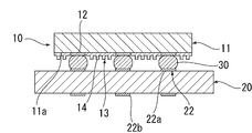
- FIG. 1 is a schematic cross-sectional view of the electronic device according to the first embodiment.
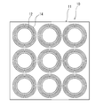
- FIG. 2 is a schematic rear view of the electronic component according to the first embodiment.
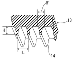
- FIG. 3 is a schematic perspective view in which a part of the resin layer in the first embodiment is enlarged.
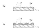
- FIG. 4A and FIG. 4B are schematic cross-sectional views for explaining a manufacturing process of the electronic device according to the first embodiment.
- FIG. 5 is a schematic cross-sectional view for explaining a manufacturing process of the electronic device according to the first embodiment.
- FIG. 6 is a schematic cross-sectional view for explaining a manufacturing process of the electronic device according to the first embodiment.
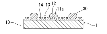
- FIG. 7 is a schematic cross-sectional view for explaining a manufacturing process of the electronic device according to the first embodiment.
- FIG. 8 is a schematic rear view of the electronic component according to the second embodiment.
- FIG. 9 is a schematic rear view of the electronic component according to the third embodiment.
- FIG. 10 is a schematic rear view of an electronic component according to
- the electronic apparatus 1 shown in FIG. 1 As an example.
- the electronic device 1 is merely an example.
- the electronic device according to the present invention is not limited to the electronic device 1.
- FIG. 1 is a schematic cross-sectional view of an electronic device according to the first embodiment.
- FIG. 2 is a schematic rear view of the electronic component according to the first embodiment.
- FIG. 3 is a schematic perspective view in which a part of the resin layer in the first embodiment is enlarged.
- the electronic device 1 includes an electronic component 10 and a resin circuit board 20.
- the type of electronic component 10 is not particularly limited.
- the electronic component 10 may be, for example, an acoustic wave device such as a surface acoustic wave device or a boundary acoustic wave device, or a semiconductor chip such as a semiconductor IC chip.
- an acoustic wave device such as a surface acoustic wave device or a boundary acoustic wave device
- a semiconductor chip such as a semiconductor IC chip.
- the electronic component 10 includes a component main body 11.
- the component main body 11 is composed of an inorganic substrate made of a semiconductor or the like.
- a plurality of terminal electrodes 12 are formed at intervals.
- the terminal electrode 12 is made of an appropriate conductive material such as a metal such as Cu, Ni, or Al, or an alloy.
- the terminal electrode 12 may be composed of a stacked body of a plurality of conductive layers, for example.
- the terminal electrode 12 may be configured by a laminated body in which, for example, a Ti layer, a Cu layer, and a Ni layer are laminated in this order from the component main body 11 side.
- a resin layer 13 as a protective layer is formed on a portion of the surface 11a of the component main body 11 where the terminal electrode 12 is not formed.
- the resin layer 13 may be formed from, for example, a photosensitive resin. That is, the resin layer 13 may be formed by curing a photosensitive resin, for example. In this case, the patterned resin layer 13 can be easily formed. Moreover, since the cured product of the photosensitive resin is excellent in chemical resistance, it is effective that the surface is eroded by the flux used for mounting by configuring the resin layer 13 with the cured product of the photosensitive resin. Can be suppressed.
- photosensitive resin examples include photosensitive polyimide, photosensitive PBO (polyparaphenylene benzobisoxazole), photosensitive BCB (benzocyclobutene), and the like.
- the resin layer 13 may be formed of a non-photosensitive resin such as a thermoplastic resin.
- the resin layer 13 can be formed at a lower cost than when the resin layer 13 is formed from a photosensitive resin.
- the resin layer 13 when forming the resin layer 13 from non-photosensitive resin, can be formed by various printing methods, such as an inkjet method, for example.
- non-photosensitive resin examples include non-photosensitive polyimide, non-photosensitive PBO, and epoxy resin.
- the average thickness of the resin layer 13 is preferably about 1 ⁇ m to 10 ⁇ m, for example.
- At least one of a concave portion and a convex portion is formed on the surface of the resin layer 13.
- a plurality of convex portions 14 are formed on the surface of the resin layer 13. As shown in FIGS. 1 and 2, the convex portion 14 is provided between the adjacent terminal electrodes 12.
- the convex portion 14 is formed in a linear shape so as to partition a region where the terminal electrode 12 is provided in a plan view (when viewed from the direction z shown in FIG. 1). More specifically, in the present embodiment, as shown in FIG. 2, the plurality of convex portions 14 are formed concentrically so as to surround the terminal electrode 12.
- the convex portion 14 is formed so that the cross-sectional shape is a substantially trapezoidal shape that tapers from the proximal end side toward the distal end side.
- the ratio (H / W) of the height H to the width W of the base portion of the convex portion 14 is preferably 0.5 or more, and more preferably 1 or more.
- the ratio (H / W) of the convex portion 14 is preferably 10 or less.
- the height H of the convex portion 14 is preferably about 1 ⁇ m to 10 ⁇ m.
- the width W of the convex portion 14 is preferably about 1 ⁇ m to 20 ⁇ m.
- the center-to-center distance L (see FIG. 3) of the protrusions 14 can be set to about 2 ⁇ m to 90 ⁇ m, for example.
- the circuit board 20 includes a circuit board main body 21.
- the circuit board body 21 is made of resin.
- the circuit board main body 21 can be comprised by a glass epoxy board
- a wiring 22 is formed on the circuit board main body 21.
- the wiring 22 is formed of an appropriate conductive material such as a metal such as Cu, Ni, or Al, or an alloy.
- the plurality of terminal electrodes 22a are terminal electrodes connected to the electronic component 10, as will be described in detail later.
- the plurality of terminal electrodes 22b are terminal electrodes used when the electronic device 1 is mounted on another circuit board.
- the electronic component 10 is mounted on the circuit board 20 with solder 30.
- the solder 30 is electrically connected by bonding the terminal electrode 12 of the electronic component 10 and the terminal electrode 22 a of the wiring 22 of the circuit board 20.
- the solder 30 is not particularly limited as long as it can suitably join the terminal electrodes 12 and 22a.
- the solder 30 can be formed of, for example, SnAgCu solder, SnAg solder, or the like.
- a resin filling layer 40 is filled between the electronic component 10 and the circuit board 20.
- the resin filling layer 40 surrounds the solder 30.
- the resin filling layer 40 is in close contact with both the surface 20 a of the circuit board 20 and the surface of the electronic component 10.
- the resin filled layer 40 is also located between the plurality of convex portions 14 of the electronic component 10, and the convex portions 14 and the resin filled layer 40 are in mesh with each other.
- the resin filling layer 40 can be formed of a known resin material such as an epoxy resin.
- the resin filling layer 40 may be made of a resin composition containing a filler, for example.
- the resin layer 13 is formed on the surface 11 a of the component main body 11.
- the resin layer 13 is formed of a photosensitive resin.
- a resin film 13a that is flush with the terminal electrode 12 is formed by spin coating or the like.
- a resin layer is formed on the resin film 13a by a spin coat method or the like, thereby forming a resin film 13b protruding from the terminal electrode 12 as shown in FIG.
- the resin layer 13 having the convex portions 14 is formed by drying, for example, at a temperature of about 250 ° C. to 400 ° C. for about 60 minutes to 90 minutes.
- the resin layer 13 when forming the resin layer 13 from non-photosensitive resin, the resin layer 13 can be formed using various printing methods and patterning methods.
- solder 30 is disposed on the circuit board 20.
- the placement of the solder 30 can be performed, for example, by mounting solder balls or plating.
- the circuit board 20 and the electronic component 10 are opposed to each other and reflowed to join the terminal electrode 12 and the terminal electrode 22 a using the solder 30.
- a resin filling layer 40 is formed by filling a resin between the electronic component 10 and the circuit board 20 to complete the electronic device 1 shown in FIG.
- the temperature of the electronic device 1 also rises.
- the component main body 11 of the electronic component 10 is formed of an inorganic substrate.
- the coefficient of thermal expansion of the component main body 11 is relatively low.
- the linear thermal expansion coefficient of silicon is about 2.4 ⁇ 10 ⁇ 6 / ° C.
- the resin filling layer 40 and the circuit board 20 are made of resin.
- the thermal expansion coefficient of the resin filling layer 40 and the circuit board 20 is relatively high.
- the linear thermal expansion coefficient of the epoxy resin below the glass transition point is about 20 ⁇ 10 ⁇ 6 / ° C.
- the linear thermal expansion coefficient of the glass epoxy substrate below the glass transition point is about 12.9 ⁇ 10 ⁇ 6 / ° C. Therefore, even if the temperature of the electronic device 1 rises, a large stress is not applied between the resin filling layer 40 and the circuit board 20, but a large stress is applied between the resin filling layer 40 and the electronic component 10. It takes. Therefore, the adhesive force at the interface between the resin filled layer 40 and the electronic component 10 tends to be reduced.
- a plurality of convex portions 14 are formed on the surface of the electronic component 10. For this reason, the adhesive force between the resin-filled layer 40 and the electronic component 10 is high. Moreover, since the resin filling layer 40 expands more thermally than the electronic component 10, the convex part 14 and the resin filling layer 40 fit more strongly. Therefore, the resin filling layer 40 and the electronic component 10 are not easily peeled off. Furthermore, even if a gap is formed between the resin-filled layer 40 and the electronic component 10, the flow of the melted solder is restricted by the convex portion 14. Therefore, it is possible to effectively prevent the molten solder 30 from flowing in the gap between the resin filling layer 40 and the electronic component 10 and short-circuiting between the terminal electrodes 12.
- the convex portion 14 is formed in a linear shape so as to partition the region where the terminal electrode 12 is provided. More specifically, the convex portion 14 is provided so as to surround the terminal electrode 12. Therefore, the adhesive force between the resin filling layer 40 and the electronic component 10 can be further increased. Moreover, the flow of the solder melted by the convex portion 14 is more effectively regulated. Therefore, a short circuit between the terminal electrodes 12 is more effectively suppressed.
- the ratio (H / W) of the height H to the width W of the base portion of the convex portion 14 is 0.5 or more. Therefore, the adhesive force between the resin-filled layer 40 and the electronic component 10 can be further increased, and the flow of molten solder can be more effectively regulated. Therefore, a short circuit between the terminal electrodes 12 is further effectively suppressed.
- solder 30 expands greatly when melted, a short circuit between the terminal electrodes 12 due to the solder 30 is more likely to occur. Therefore, the technique of this embodiment that can suppress a short circuit between the terminal electrodes 12 is particularly effective when the solder 30 expands greatly when melted.
- Specific examples of solder that expands greatly when melted include SnAgCu solder, SnAg solder, and the like.
- the surface of the electronic component is roughened, the surface area of the electronic component increases, but the adhesion between the electronic component and the resin-filled layer is not sufficiently improved. Therefore, a short circuit between the terminal electrodes cannot be sufficiently suppressed.
- FIG. 1 is referred to in common with the first embodiment.
- FIG. 8 is a schematic rear view of the electronic component according to the second embodiment.
- the shape of the convex portion 14 is not limited to the shape of the first embodiment.
- the convex part 14 may be formed, for example, in a square shape in plan view.
- the convex part 14 may be formed in planar view polygonal shape, elliptical shape, an ellipse shape, etc.
- FIG. 9 is a schematic rear view of the electronic component according to the third embodiment.
- FIG. 10 is a schematic rear view of an electronic component according to the fourth embodiment.
- the convex portion 14 is formed so as to surround the terminal electrode 12 has been described.
- the present invention is not limited to this configuration.
- the convex portion 14 may be provided so as not to surround the terminal electrode 12.
- the convex portion 14 is formed in an L shape between the adjacent terminal electrodes 12.
- the convex portion 14 is formed in an arc shape between the adjacent terminal electrodes 12.
- the convex portion 14 is provided on the surface of the resin layer 13 .
- at least one of the concave portion and the convex portion may be directly provided on the surface of the component main body.
Landscapes
- Wire Bonding (AREA)
- Electric Connection Of Electric Components To Printed Circuits (AREA)
Abstract
電子部品が半田により実装されている回路基板を備える電子装置であって、フリップチップ実装時に端子電極間の短絡が生じにくい電子装置を提供する。 電子装置1は、複数の端子電極12を有する電子部品10と、配線22が形成されている回路基板20と、配線22と、端子電極12とを接合している半田30と、半田30を包囲するように、電子部品10と回路基板20との間に充填されている樹脂充填層40とを備えている。電子部品10の端子電極12が形成されている側の表面において、隣接している端子電極12の間に、凹部及び凸部14のうちの少なくとも一方が形成されている。
Description
本発明は、電子装置に関する。特に、本発明は、電子部品と、電子部品が半田により実装されている回路基板と、電子部品と回路基板との間に充填された樹脂充填層とを備える電子装置に関する。
半導体素子などの電子部品が半田により実装されている回路基板を備える電子装置が、さらに他の回路基板に実装される場合がある。このように、さらに他の回路基板に実装される電子装置では、他の回路基板への実装時に電子部品と回路基板とを接合している半田が融解し、端子電極間が短絡する場合があるという問題がある。
例えば下記の特許文献1には、このような問題を解決し得るものとして、以下のような半導体装置が開示されている。すなわち、特許文献1に記載の半導体装置は、半導体素子と、半導体素子が実装された半導体キャリア基板と、半導体素子と半導体キャリア基板との間に充填されている樹脂充填層とを備えている。特許文献1の半導体装置では、半導体キャリア基板側の配線は、半導体キャリア基板に形成された凹部内に形成されており、かつ、その配線と半導体素子とを接合している半田も、凹部内に設けられている。このため、半導体装置を実装する際に半田が融解したとしても、端子電極間の短絡が生じ難い旨が、特許文献1に記載されている。
しかしながら、本発明者が鋭意研究した結果、特許文献1に記載の技術を適用したとしても、実装時において半田が融解することに起因する端子電極間の短絡を十分に抑制できないことが見出された。
本発明は、かかる点に鑑みてなされたものであり、その目的は、電子部品が半田により実装されている回路基板を備える電子装置であって、実装時に端子電極間の短絡が生じにくい電子装置を提供することにある。
本発明者は、鋭意研究の結果、半田の融解による端子電極間の短絡は、主として、半田が電子部品と樹脂充填層との間の隙間を流動することにより発生しているため、上記特許文献1に記載の技術では、端子間の短絡を十分に抑制できないことを見出した。その結果、本発明者らは、本発明を成すに至った。
本発明に係る電子装置は、電子部品と、回路基板と、半田と、樹脂充填層とを備えている。電子部品は、複数の端子電極を有する。回路基板には、配線が形成されている。半田は、配線と、端子電極とを接合している。樹脂充填層は、半田を包囲するように、電子部品と回路基板との間に充填されている。電子部品の端子電極が形成されている側の表面において、隣接している端子電極の間に、凹部及び凸部のうちの少なくとも一方が形成されている。
本発明に係る電子装置のある特定の局面では、凹部及び凸部のうちの少なくとも一方は、平面視において、端子電極が設けられている領域を区画するように線状に形成されている。この構成によれば、電子部品と樹脂充填層との間に、融解した半田が流入して端子電極間が短絡することをより効果的に抑制することができる。
なお、本発明において、「線状」には、「直線状」、「曲線状」及び「クランク状」が含まれるものとする。
本発明に係る電子装置の他の特定の局面では、凹部及び凸部のうちの少なくとも一方は、端子電極を包囲するように設けられている。この構成によれば、電子部品と樹脂充填層との間に、融解した半田が流入して端子電極間が短絡することをさらに効果的に抑制することができる。
本発明に係る電子装置の別の特定の局面では、回路基板は、樹脂製である。この構成では、回路基板と樹脂充填層との間の熱膨張率差を小さくすることができる。このため、回路基板と樹脂充填層との間に隙間が生じることをより効果的に抑制することができる。従って、融解した半田の流動による端子電極間の短絡をより効果的に抑制することができる。
なお、本発明において、「樹脂製の回路基板」には、例えば、ガラスファイバーが混入しているガラスエポキシ基板などの、無機部材が混入している樹脂からなる回路基板も含まれるものとする。
本発明に係る電子装置のさらに他の特定の局面では、電子部品は、複数の端子電極が形成されている無機基板をさらに有する。この場合、電子部品と樹脂充填層との間に隙間ができやすく、融解した半田がその隙間を流動することにより端子電極間が短絡しやすくなるため、端子電極間の短絡を抑制できる本発明が特に有効である。
本発明に係る電子装置のさらに別の特定の局面では、電子部品は、半導体チップである。
本発明に係る電子装置のさらにまた他の特定の局面では、電子部品は、部品本体と、樹脂層とをさらに有する。部品本体には、複数の端子電極が形成されている。樹脂層は、部品本体の複数の端子電極が形成されている側の表面上に設けられている。樹脂層の表面には、上記凹部及び凸部のうちの少なくとも一方を構成している凹凸が形成されている。樹脂層は、感光性樹脂が硬化してなるものである。この構成では、容易かつ高精度に凹凸が形成された樹脂層を形成することができる。従って、電子装置の製造容易性が向上する。また、感光性樹脂の硬化物は、耐薬品性に優れているため、実装に使用されるフラックスによって表面が侵されることを効果的に抑制することができる。
本発明に係る電子装置のさらにまた別の特定の局面では、凹部及び凸部のうちの少なくとも一方の、基底部の幅に対する高さの比(高さ/基底部の幅)が0.5以上10以下である。この構成によれば、電子部品と樹脂充填層との密着性をより高めることができる。このため、融解した半田の流動による端子電極間の短絡をさらに効果的に抑制することができる。
本発明では、電子部品の端子電極が形成されている側の表面において、隣接している端子電極の間に、凹部及び凸部のうちの少なくとも一方が形成されている。このため、電子部品と樹脂充填層との密着性を高めることができる。よって、電子部品と樹脂充填層との間に隙間が生じ難く、融解した半田がその隙間を経由して端子電極間を流動することにより生じる端子電極間の短絡を抑制することができる。従って、本発明によれば、フリップチップ実装時に端子電極間の短絡が生じにくい電子装置を提供することができる。
以下、本発明を実施した好ましい形態について、図1に示す電子装置1を例に挙げて説明する。但し、電子装置1は、単なる例示である。本発明に係る電子装置は、電子装置1に何ら限定されない。
(第1の実施形態)
図1は、第1の実施形態に係る電子装置の略図的断面図である。図2は、第1の実施形態における電子部品の略図的裏面図である。図3は、第1の実施形態における樹脂層の一部分を拡大した略図的斜視図である。
図1は、第1の実施形態に係る電子装置の略図的断面図である。図2は、第1の実施形態における電子部品の略図的裏面図である。図3は、第1の実施形態における樹脂層の一部分を拡大した略図的斜視図である。
まず、図1~図3を参照しながら、本実施形態の電子装置1の構成について詳細に説明する。
図1に示すように、電子装置1は、電子部品10と、樹脂製の回路基板20とを備えている。
電子部品10の種類は、特に限定されない。電子部品10は、例えば、弾性表面波素子や弾性境界波素子などの弾性波素子であってもよいし、半導体ICチップなどの半導体チップであってもよい。以下、本実施形態では、電子部品10が半導体ICチップである場合について説明する。
電子部品10は、部品本体11を備えている。本実施形態では、部品本体11は、半導体などからなる無機基板により構成されている。部品本体11の回路基板20側の表面11aの上には、複数の端子電極12が間隔をおいて形成されている。端子電極12は、例えば、Cu,Ni,Alなどの金属や合金などの適宜の導電材料により形成されている。端子電極12は、例えば、複数の導電層の積層体により構成されていてもよい。具体的には、端子電極12は、例えば、部品本体11側から、Ti層、Cu層及びNi層がこの順番で積層された積層体により構成されていてもよい。
部品本体11の表面11aのうち、端子電極12が形成されていない部分の上には、保護層としての樹脂層13が形成されている。樹脂層13は、例えば、感光性樹脂から形成されていてもよい。すなわち、樹脂層13は、例えば、感光性樹脂が硬化されてなるものであってもよい。この場合、パターニングされた樹脂層13を容易に形成することができる。また、感光性樹脂の硬化物は、耐薬品性に優れているため、樹脂層13を感光性樹脂の硬化物により構成することで、実装に使用されるフラックスによって表面が侵されることを効果的に抑制することができる。
感光性樹脂の具体例としては、例えば、感光性ポリイミド、感光性PBO(ポリパラフェニレンベンゾビスオキサゾール(poly-phenylene-benzobisoxazole))、感光性BCB(ベンゾシクロブテン(Benzocyclobutene))などが挙げられる。
また、樹脂層13は、例えば熱可塑性樹脂などの非感光性樹脂から形成されていてもよい。この場合は、樹脂層13を感光性樹脂から形成する場合よりも安価に樹脂層13を形成することができる。なお、樹脂層13を非感光性樹脂から形成する場合、樹脂層13は、例えば、インクジェット法などの各種印刷法により形成することができる。
非感光性樹脂の具体例としては、例えば、非感光性ポリイミド、非感光性PBO、エポキシ系樹脂などが挙げられる。
樹脂層13の平均厚みは、例えば、1μm~10μm程度であることが好ましい。
本実施形態では、樹脂層13の表面に凹部及び凸部のうちの少なくとも一方が形成されている。具体的には、本実施形態では、樹脂層13の表面に、複数の凸部14が形成されている。図1及び図2に示すように、凸部14は、隣接している端子電極12間に設けられている。
より具体的には、凸部14は、平面視において(図1に示す方向zから視た際において)、端子電極12が設けられている領域を区画するように線状に形成されている。さらに具体的には、本実施形態では、図2に示すように、複数の凸部14は、端子電極12を包囲するように、同心円状に形成されている。
図3に示すように、凸部14は、横断面形状が基端側から先端側に向かって先細る略台形状となるように形成されている。凸部14の基底部の幅Wに対する高さHの比(H/W)は、0.5以上であることが好ましく、1以上であることがさらに好ましい。但し、凸部14の比(H/W)が大きすぎると、実装時に凸部14と半田とが干渉してしまい、実装不良が生じる場合がある。また、凸部14の機械的強度が低くなると共に、凸部14の形成が困難となる場合がある。従って、凸部14の比(H/W)は、10以下であることが好ましい。
凸部14の高さHは、1μm~10μm程度であることが好ましい。凸部14の幅Wは、1μm~20μm程度であることが好ましい。凸部14の中心間距離L(図3を参照)は、例えば、2μm~90μm程度とすることができる。
回路基板20は、回路基板本体21を備えている。回路基板本体21は、樹脂製である。具体的には、回路基板本体21は、例えば、ガラスエポキシ基板などにより構成することができる。
回路基板本体21には、配線22が形成されている。配線22は、例えば、Cu,Ni,Alなどの金属や合金などの適宜の導電材料により形成されている。
配線22には、回路基板20の電子部品10側の表面20a上に形成されている複数の端子電極22aと、回路基板20の電子部品10とは反対側の表面20b上に形成されている複数の端子電極22bとを備えている。複数の端子電極22aは、後に詳述するように、電子部品10と接続される端子電極である。一方、複数の端子電極22bは、電子装置1が、別の回路基板に実装される際に使用される端子電極である。
電子部品10は、半田30により、回路基板20に実装されている。半田30は、電子部品10の端子電極12と、回路基板20の配線22の端子電極22aとを接合することにより電気的に接続している。
半田30は、端子電極12,22a間を好適に接合できるものである限りにおいて特に限定されない。半田30は、例えば、SnAgCu系半田、SnAg系半田などにより形成することができる。
電子部品10と回路基板20との間には、樹脂充填層40が充填されている。この樹脂充填層40により、半田30が包囲されている。樹脂充填層40は、回路基板20の表面20aと、電子部品10の表面との両方に密着している。樹脂充填層40は、電子部品10の複数の凸部14間にも位置しており、凸部14と樹脂充填層40とは、かみ合った状態となっている。樹脂充填層40は、例えばエポキシ系樹脂などの公知の樹脂材料により形成することができる。樹脂充填層40は、例えば、フィラー等を含む樹脂組成物からなるものであってもよい。
次に、電子装置1の製造方法の一例について、図4~図7を主として参照しながら説明する。但し、下記の製造方法は単なる一例であって、本発明は、下記の製造方法に何ら限定されない。
まず、部品本体11の表面11aの上に、樹脂層13を形成する。なお、ここでは、樹脂層13を感光性樹脂により形成する場合について説明する。具体的には、まず、図4(a)に示すように、端子電極12と面一である樹脂膜13aをスピンコート法などにより形成する。さらに、スピンコート法などにより、樹脂膜13aの上に、樹脂層を形成することにより、図4(b)に示すように、端子電極12よりも突出した樹脂膜13bを形成する。
次に、樹脂膜13bを、露光及び現像した後に、例えば、250℃~400℃程度の温度で、60分~90分程度乾燥させることにより、凸部14を有する樹脂層13を形成する。
なお、樹脂層13を非感光性樹脂から形成する場合は、樹脂層13を、各種印刷法やパターニング方法を用いて形成することができる。
次に、図6に示すように、回路基板20上に、半田30を配置する。半田30の配置は、例えば、半田ボールの搭載や、めっきなどにより行うことができる。その後、図7に示すように、回路基板20と電子部品10とを対向させ、リフローすることにより、半田30を用いて端子電極12と端子電極22aとを接合する。
最後に、電子部品10と回路基板20との間に樹脂を充填することにより、樹脂充填層40を形成し、図1に示す電子装置1を完成させる。
ところで、電子装置1を他の回路基板に二次実装する場合、電子装置1の温度も上昇する。ここで、電子部品10の部品本体11は、無機基板により構成されている。このため、部品本体11の熱膨張率は、比較的低い。例えば、シリコンの線熱膨張係数は、2.4×10⁻⁶/℃程度である。それに対して、樹脂充填層40と、回路基板20とは、樹脂製である。このため、樹脂充填層40と、回路基板20との熱膨張率は、比較的高い。例えば、エポキシ樹脂のガラス転移点以下における線熱膨張係数は、20×10-6/℃程度である。ガラスエポキシ基板のガラス転移点以下における線熱膨張係数は、12.9×10-6/℃程度である。従って、電子装置1の温度が上昇しても、樹脂充填層40と回路基板20との間には、それほど大きな応力がかからないものの、樹脂充填層40と電子部品10との間には、大きな応力がかかる。よって、樹脂充填層40と電子部品10との間の界面の密着力が低下しがちである。
しかしながら、本実施形態では、電子部品10の表面に複数の凸部14が形成されている。このため、樹脂充填層40と電子部品10との密着力が高い。また、樹脂充填層40は電子部品10よりも大きく熱膨張するため、凸部14と樹脂充填層40とがより強く嵌合する。よって、樹脂充填層40と電子部品10とが剥がれにくい。さらに、仮に樹脂充填層40と電子部品10との間に隙間が形成されたとしても、凸部14により融解した半田の流動が規制される。従って、融解した半田30が、樹脂充填層40と電子部品10との間の隙間を流動し、端子電極12間が短絡することが効果的に抑制される。
また、本実施形態では、凸部14が、端子電極12が設けられている領域を区画するように線状に形成されている。より詳細には、凸部14は、端子電極12を包囲するように設けられている。従って、樹脂充填層40と電子部品10との密着力をより高くすることができる。また、凸部14により融解した半田の流動がより効果的に規制される。従って、端子電極12間が短絡することがより効果的に抑制される。
さらに、本実施形態では、凸部14の基底部の幅Wに対する高さHの比(H/W)が、0.5以上である。従って、樹脂充填層40と電子部品10との密着力をさらに高くでき、かつ融解した半田の流動をさらに効果的に規制することができる。従って、端子電極12間が短絡することがさらに効果的に抑制される。
上記効果は、半田30の種類に関わらず奏されるものである。但し、半田30が、融解したときに大きく膨張するものである場合は、半田30による端子電極12間の短絡がより発生しやすくなる。従って、端子電極12間の短絡を抑制できる本実施形態の技術は、半田30が、融解したときに大きく膨張するものである場合に特に有効である。融解したときに大きく膨張する半田の具体例としては、例えば、SnAgCu系半田、SnAg系半田などが挙げられる。
なお、例えば、電子部品の表面に粗面化処理した場合、電子部品の表面面積は、増大するが、電子部品と樹脂充填層との密着性は、十分に向上しない。従って、端子電極間の短絡を十分に抑制することはできない。
以下、本発明を実施した好ましい形態の他の例について説明する。以下の説明において、上記第1の実施形態と実質的に共通の機能を有する部材を共通の符号で参照し、説明を省略する。また、図1を上記第1の実施形態と共通に参照する。
(第2の実施形態)
図8は、第2の実施形態における電子部品の略図的裏面図である。
図8は、第2の実施形態における電子部品の略図的裏面図である。
上記第1の実施形態では、凸部14が円環状に形成されている例について説明した。但し、本発明において、凸部14の形状は、上記第1の実施形態の形状に限定されない。例えば、図8に示すように、凸部14は、例えば、平面視四角形状に形成されていてもよい。また、凸部14は、平面視多角形状、楕円形状、長円形状などに形成されていてもよい。
(第3及び第4の実施形態)
図9は、第3の実施形態における電子部品の略図的裏面図である。図10は、第4の実施形態における電子部品の略図的裏面図である。
図9は、第3の実施形態における電子部品の略図的裏面図である。図10は、第4の実施形態における電子部品の略図的裏面図である。
上記第1及び第2の実施形態では、凸部14が端子電極12を包囲するように形成されている例について説明した。但し、本発明は、この構成に限定されない。例えば、図9や図10に示すように、凸部14を、端子電極12を包囲しないように設けてもよい。
具体的には、図9に示す例では、凸部14は、隣接する端子電極12間において、L字状に形成されている。図10に示す例では、凸部14は、隣接する端子電極12間において、円弧状に形成されている。
図9及び図10に示すように、凸部14が、平面視において、端子電極12が設けられている領域を区画するように線状に設けられている場合は、上記第1の実施形態と同様に、端子電極12間が短絡することを効果的に抑制することができる。
なお、上記実施形態では、樹脂層13の表面に凸部14を設ける例について説明したが、部品本体の表面に、凹部及び凸部のうちの少なくとも一方を直接設けてもよい。
1…電子装置
10…電子部品
11…部品本体
11a…部品本体の表面
12…電子部品の端子電極
13…樹脂層
13a、13b…樹脂膜
14…凸部
20…回路基板
20a、20b…回路基板の表面
21…回路基板本体
22…配線
22a、22b…回路基板の端子電極
30…半田
40…樹脂充填層
10…電子部品
11…部品本体
11a…部品本体の表面
12…電子部品の端子電極
13…樹脂層
13a、13b…樹脂膜
14…凸部
20…回路基板
20a、20b…回路基板の表面
21…回路基板本体
22…配線
22a、22b…回路基板の端子電極
30…半田
40…樹脂充填層
Claims (8)
- 複数の端子電極を有する電子部品と、
配線が形成されている回路基板と、
前記配線と、前記端子電極とを接合している半田と、
前記半田を包囲するように、前記電子部品と前記回路基板との間に充填されている樹脂充填層とを備え、
前記電子部品の前記端子電極が形成されている側の表面において、隣接している前記端子電極の間に、凹部及び凸部のうちの少なくとも一方が形成されている、電子装置。 - 前記凹部及び凸部のうちの少なくとも一方は、平面視において、前記端子電極が設けられている領域を区画するように線状に形成されている、請求項1に記載の電子装置。
- 前記凹部及び凸部のうちの少なくとも一方は、前記端子電極を包囲するように設けられている、請求項1または2に記載の電子装置。
- 前記回路基板は、樹脂製である、請求項1~3のいずれか一項に記載の電子装置。
- 前記電子部品は、前記複数の端子電極が形成されている無機基板をさらに有する、請求項1~4のいずれか一項に記載の電子装置。
- 前記電子部品は、半導体チップである、請求項1~5のいずれか一項に記載の電子装置。
- 前記電子部品は、前記複数の端子電極が形成されている部品本体と、前記部品本体の前記複数の端子電極が形成されている側の表面上に設けられており、前記凹部及び凸部のうちの少なくとも一方を構成している凹凸が表面に形成されている樹脂層とをさらに有し、
前記樹脂層は、感光性樹脂が硬化してなるものである、請求項1~6のいずれか一項に記載の電子装置。 - 前記凹部及び凸部のうちの少なくとも一方の、基底部の幅に対する高さの比(高さ/基底部の幅)が0.5以上10以下である、請求項1~7のいずれか一項に記載の電子装置。
Applications Claiming Priority (2)
| Application Number | Priority Date | Filing Date | Title |
|---|---|---|---|
| JP2010087747A JP2013131508A (ja) | 2010-04-06 | 2010-04-06 | 電子装置 |
| JP2010-087747 | 2010-04-06 |
Publications (1)
| Publication Number | Publication Date |
|---|---|
| WO2011125434A1 true WO2011125434A1 (ja) | 2011-10-13 |
Family
ID=44762394
Family Applications (1)
| Application Number | Title | Priority Date | Filing Date |
|---|---|---|---|
| PCT/JP2011/056156 Ceased WO2011125434A1 (ja) | 2010-04-06 | 2011-03-16 | 電子装置 |
Country Status (2)
| Country | Link |
|---|---|
| JP (1) | JP2013131508A (ja) |
| WO (1) | WO2011125434A1 (ja) |
Cited By (2)
| Publication number | Priority date | Publication date | Assignee | Title |
|---|---|---|---|---|
| CN114097015A (zh) * | 2019-07-12 | 2022-02-25 | 夏普株式会社 | 显示装置 |
| US11830835B2 (en) | 2020-08-26 | 2023-11-28 | Infineon Technologies Ag | Chip with chip pad and associated solder flux outgassing trench |
Families Citing this family (2)
| Publication number | Priority date | Publication date | Assignee | Title |
|---|---|---|---|---|
| CN109545754B (zh) * | 2018-11-22 | 2021-01-26 | 京东方科技集团股份有限公司 | 一种芯片的封装结构、封装方法、显示装置 |
| CN110211935A (zh) * | 2019-05-08 | 2019-09-06 | 华为技术有限公司 | 一种防止分层窜锡的封装及制造方法 |
Citations (2)
| Publication number | Priority date | Publication date | Assignee | Title |
|---|---|---|---|---|
| JP2005079499A (ja) * | 2003-09-03 | 2005-03-24 | Seiko Epson Corp | 半導体装置、半導体モジュール、電子機器および半導体装置の製造方法 |
| JP2009188275A (ja) * | 2008-02-07 | 2009-08-20 | Sharp Corp | 半導体チップ、半導体装置、半導体装置の製造方法、および液晶モジュール |
-
2010
- 2010-04-06 JP JP2010087747A patent/JP2013131508A/ja not_active Withdrawn
-
2011
- 2011-03-16 WO PCT/JP2011/056156 patent/WO2011125434A1/ja not_active Ceased
Patent Citations (2)
| Publication number | Priority date | Publication date | Assignee | Title |
|---|---|---|---|---|
| JP2005079499A (ja) * | 2003-09-03 | 2005-03-24 | Seiko Epson Corp | 半導体装置、半導体モジュール、電子機器および半導体装置の製造方法 |
| JP2009188275A (ja) * | 2008-02-07 | 2009-08-20 | Sharp Corp | 半導体チップ、半導体装置、半導体装置の製造方法、および液晶モジュール |
Cited By (3)
| Publication number | Priority date | Publication date | Assignee | Title |
|---|---|---|---|---|
| CN114097015A (zh) * | 2019-07-12 | 2022-02-25 | 夏普株式会社 | 显示装置 |
| US11830835B2 (en) | 2020-08-26 | 2023-11-28 | Infineon Technologies Ag | Chip with chip pad and associated solder flux outgassing trench |
| US12132017B2 (en) | 2020-08-26 | 2024-10-29 | Infineon Technologies Ag | Method of soldering a semiconductor chip to a chip carrier |
Also Published As
| Publication number | Publication date |
|---|---|
| JP2013131508A (ja) | 2013-07-04 |
Similar Documents
| Publication | Publication Date | Title |
|---|---|---|
| JP5664392B2 (ja) | 半導体装置、半導体装置の製造方法、及び配線基板の製造方法 | |
| JP5649805B2 (ja) | 半導体装置の製造方法 | |
| JP2011134818A (ja) | 半導体素子内蔵基板 | |
| CN103299410B (zh) | 电子元器件模块及电子元器件单元 | |
| KR20040100949A (ko) | 반도체 패키지의 제조 방법, 및 반도체 장치의 제조 방법 | |
| KR101140518B1 (ko) | 배선 기판 및 반도체 장치 | |
| JP2010165923A (ja) | 半導体装置、及びその製造方法 | |
| US7928559B2 (en) | Semiconductor device, electronic component module, and method for manufacturing semiconductor device | |
| JP4916241B2 (ja) | 半導体装置及びその製造方法 | |
| US9426887B2 (en) | Wiring board and electronic device using the same | |
| WO2011125434A1 (ja) | 電子装置 | |
| JP2009200067A (ja) | 半導体チップおよび半導体装置 | |
| CN103378041A (zh) | 迹线上凸块芯片封装的方法和装置 | |
| JP2010232616A (ja) | 半導体装置及び配線基板 | |
| JP2008177619A (ja) | チップキャリア及び半導体装置並びにチップキャリアの製造方法 | |
| JP4172238B2 (ja) | 電子部品の実装構造 | |
| KR101596074B1 (ko) | 전자부품 실장용 배선기판의 제조방법, 전자부품 실장용 배선기판, 및 전자부품을 가진 배선기판의 제조방법 | |
| US8168525B2 (en) | Electronic part mounting board and method of mounting the same | |
| JP2005026364A (ja) | 混成集積回路 | |
| JP2016127066A (ja) | バンプ付きプリント配線板およびその製造方法 | |
| JP6464762B2 (ja) | 半導体パッケージ基板、および半導体パッケージと、半導体パッケージ基板の製造方法、および半導体パッケージの製造方法 | |
| JPH11214432A (ja) | 半導体装置およびスペーサ形成方法 | |
| JP5482170B2 (ja) | 半導体装置、半導体装置の製造方法、回路基板及び回路基板の製造方法 | |
| JP7416607B2 (ja) | 半導体装置 | |
| JP3658156B2 (ja) | 実装体及びその製造方法 |
Legal Events
| Date | Code | Title | Description |
|---|---|---|---|
| 121 | Ep: the epo has been informed by wipo that ep was designated in this application |
Ref document number: 11765336 Country of ref document: EP Kind code of ref document: A1 |
|
| NENP | Non-entry into the national phase |
Ref country code: DE |
|
| 122 | Ep: pct application non-entry in european phase |
Ref document number: 11765336 Country of ref document: EP Kind code of ref document: A1 |
|
| NENP | Non-entry into the national phase |
Ref country code: JP |