WO2011125408A1 - タッチパネルおよびタッチパネルを備える入出力装置 - Google Patents
タッチパネルおよびタッチパネルを備える入出力装置 Download PDFInfo
- Publication number
- WO2011125408A1 WO2011125408A1 PCT/JP2011/055611 JP2011055611W WO2011125408A1 WO 2011125408 A1 WO2011125408 A1 WO 2011125408A1 JP 2011055611 W JP2011055611 W JP 2011055611W WO 2011125408 A1 WO2011125408 A1 WO 2011125408A1
- Authority
- WO
- WIPO (PCT)
- Prior art keywords
- touch panel
- piezoelectric sheet
- electrode
- input
- output device
- Prior art date
Links
Images


Classifications
-
- G—PHYSICS
- G06—COMPUTING; CALCULATING OR COUNTING
- G06F—ELECTRIC DIGITAL DATA PROCESSING
- G06F3/00—Input arrangements for transferring data to be processed into a form capable of being handled by the computer; Output arrangements for transferring data from processing unit to output unit, e.g. interface arrangements
- G06F3/01—Input arrangements or combined input and output arrangements for interaction between user and computer
- G06F3/016—Input arrangements with force or tactile feedback as computer generated output to the user
-
- G—PHYSICS
- G06—COMPUTING; CALCULATING OR COUNTING
- G06F—ELECTRIC DIGITAL DATA PROCESSING
- G06F3/00—Input arrangements for transferring data to be processed into a form capable of being handled by the computer; Output arrangements for transferring data from processing unit to output unit, e.g. interface arrangements
- G06F3/01—Input arrangements or combined input and output arrangements for interaction between user and computer
- G06F3/03—Arrangements for converting the position or the displacement of a member into a coded form
- G06F3/041—Digitisers, e.g. for touch screens or touch pads, characterised by the transducing means
- G06F3/0414—Digitisers, e.g. for touch screens or touch pads, characterised by the transducing means using force sensing means to determine a position
-
- H—ELECTRICITY
- H10—SEMICONDUCTOR DEVICES; ELECTRIC SOLID-STATE DEVICES NOT OTHERWISE PROVIDED FOR
- H10N—ELECTRIC SOLID-STATE DEVICES NOT OTHERWISE PROVIDED FOR
- H10N30/00—Piezoelectric or electrostrictive devices
- H10N30/20—Piezoelectric or electrostrictive devices with electrical input and mechanical output, e.g. functioning as actuators or vibrators
- H10N30/204—Piezoelectric or electrostrictive devices with electrical input and mechanical output, e.g. functioning as actuators or vibrators using bending displacement, e.g. unimorph, bimorph or multimorph cantilever or membrane benders
- H10N30/2047—Membrane type
Definitions
- the present invention relates to a touch panel and an input / output device configured using the touch panel, and more particularly to a technique for improving detection accuracy for a pressing operation position of the touch panel.
- FIG. 3 of Patent Document 1 shows a display operation unit in an information display device provided in an automatic teller machine.
- the display operation unit houses a liquid crystal display panel in a case having a window, and the main surface of the liquid crystal display panel is an information display surface.
- An operation panel is arranged in parallel to the information display surface of the liquid crystal display panel at a predetermined interval.
- Piezoelectric elements are arranged near the four corners of the liquid crystal display panel and on the bottom surface of the case, and the operation panel is supported by these piezoelectric elements.
- an object of the present invention is to provide a touch panel that can solve the above-described problems, and an input / output device that uses the touch panel.
- the piezoelectric sheet having piezoelectricity and the first and second opposing surfaces formed on the first and second main surfaces of the piezoelectric sheet facing each other, respectively.
- a second electrode a protective film that is attached to the first main surface side of the piezoelectric sheet and constitutes an operation surface to be pressed by the operator, and is disposed on the second main surface side of the piezoelectric sheet.
- a substrate a substrate.
- the first and second electrodes is a divided electrode having a plurality of electrode portions that are electrically insulated from each other.
- a rubber-like elastic body is disposed between the piezoelectric sheet and the base body in order to increase the detection accuracy of the pressing operation position.
- the piezoelectric sheet is an L-type polylactic acid sheet having a stretching axis facing a predetermined direction.
- the piezoelectric sheet, the first and second electrodes, the protective film, and the rubber-like elastic body preferably have transparency.
- An input / output device includes an operation signal extraction means for extracting an electric signal output from each of the plurality of electrode portions of the divided electrode as an operation signal in response to a pressing operation to an arbitrary position on the operation surface; Drive signal feedback means for feeding back a drive signal to each of the plurality of electrode portions of the divided electrode in response to the signal is provided.
- the touch panel is configured to emit a sound to the operator by a driving signal or to give a tactile sensation to the operator, both of them are executed. May be.
- the present invention it is possible to acquire three-dimensional pressing operation information such as detection of the pressing operation position and detection of pressing force, and it is possible to give sound and tactile sensation to the operator by the piezoelectric sheet itself. In spite of having such multiple functions, a touch panel with a small thickness can be realized.
- the rubber-like elastic body is disposed between the piezoelectric sheet and the base body, it is possible to improve the detection accuracy of the pressing operation position.
- the base is constituted by a flat panel display, for example.
- a pressing operation can be performed while viewing the flat panel display by arranging a flat panel display under the transparent structure.
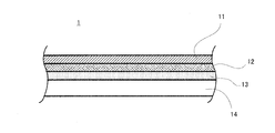
- FIG. 1 is a perspective view showing an appearance of a touch panel 1 according to a first embodiment of the present invention. It is sectional drawing of the touch panel 1 shown in FIG. It is a perspective view which shows the piezoelectric sheet 12 with which the touch panel 1 shown in FIG. 1 is equipped. It is the top view which showed the piezoelectric sheet 12 shown in FIG. 3 from the 1st main surface 12a side. This is for explaining the problems of the touch panel as a comparative example of the present invention. In the touch panel 1 shown in FIG. 2, the rubber-like elastic body 13 is eliminated, and a small space is formed between the base 14 and the piezoelectric sheet 12. It is a figure which shows the voltage measurement value in the case of being carried out.
- FIG. 4 is a diagram illustrating a result of calculation by a finite element method simulation of a fundamental vibration mode of the piezoelectric sheet 12 when a signal voltage is applied to each of electrode portions 2a to 2d illustrated in FIG. It is a figure which shows schematically the circuit structure of the input / output device 5 comprised using the touch panel 1 shown in FIG. It is a figure corresponding to FIG. 4 which shows 2nd Embodiment of this invention.
- FIG. 4 shows the 3rd Embodiment of this invention. It is a figure corresponding to FIG. 4 which shows 4th Embodiment of this invention. It is a figure corresponding to FIG. 4 which shows the 5th Embodiment of this invention. It is a figure corresponding to Drawing 4 showing the 6th embodiment of this invention. It is a figure for demonstrating the application method of the voltage at the time of driving the touch panel which concerns on embodiment shown in FIG. 13 as a speaker or tactile feedback. It is a figure for demonstrating the other example of the application method of the voltage at the time of driving the touchscreen which concerns on embodiment shown in FIG. 13 as a speaker or tactile feedback.
- FIG. 16 is a diagram showing a state of vibration when a vibration signal is given only to the hatched electrode portions 55 to 58 in FIG. 15 by simulation using a finite element method.
- FIG. 1 is a perspective view showing the appearance of the touch panel 1 according to the first embodiment of the present invention. A cross-sectional view of the touch panel 1 is shown in FIG.
- the touch panel 1 has a cross-sectional structure in which a protective film 11, a piezoelectric sheet 12, a rubber-like elastic body 13, and a base 14 are laminated in this order.
- the touch panel 1 is usually disposed on the surface of a flat panel display (FPD) such as a liquid crystal display or an organic EL display. Therefore, each element constituting the touch panel 1 is preferably made of a material having transparency.
- the protective film 11 constitutes an operation surface to be pressed by an operator, and the surface thereof is omitted from illustration, but is provided with a hard coat for preventing an antireflection film and preventing scratches and dirt. There is a case.
- FIG. 3 shows the piezoelectric sheet 12 in a perspective view.
- the piezoelectric sheet 12 is preferably made of L-type polylactic acid (PLLA).
- the piezoelectric sheet 12 made of PLLA is provided with piezoelectricity by being stretched and heat-treated.
- the piezoelectric sheet 12 has a stretching axis 15 facing in the direction of the arrow.
- the electrode 2 is illustrated.
- first and second electrodes facing each other are formed, respectively.
- These electrodes are preferably made of a transparent material such as indium tin oxide, indium zinc oxide, zinc oxide, polythiophene conductive polymer, and aniline conductive polymer.
- a transparent material such as indium tin oxide, indium zinc oxide, zinc oxide, polythiophene conductive polymer, and aniline conductive polymer.
- a transparent material such as indium tin oxide, indium zinc oxide, zinc oxide, polythiophene conductive polymer, and aniline conductive polymer.
- At least one of the first and second electrodes is a divided electrode having a plurality of electrode portions that are electrically insulated from each other.
- 3 and 4 show the first main surface 12a side of the piezoelectric sheet 12.
- FIG. The first main surface 12a may be a main surface facing upward or a surface facing downward in FIG.
- a first electrode 2 is formed on the first main surface 12a, and the first electrode 2 is a divided electrode having, for example, four electrode portions 2a to 2d.
- the protective film 11 is made of, for example, polyethylene terephthalate or polyethylene naphthalate.
- the substrate 14 is also composed of, for example, polyethylene terephthalate or polyethylene naphthalate, but may instead be provided by FPD.
- the protective film 11 is preferably thinner than the substrate 14.
- the rubber-like elastic body 13 is a rubber state and is an elastic body having rubber elasticity (entropic elasticity).
- the material constituting the rubber-like elastic body 13 is preferably a highly transparent material such as polyurethane rubber or silicone rubber, and preferably has a hardness of Hs 20 to 50.
- the thickness, type, and hardness of the rubber used are design matters determined in view of the thickness and hardness of the protective film 11, the thickness of the piezoelectric sheet 12, the piezoelectric constant, detection accuracy, and the like.
- voltage information obtained from the voltage generated in each of the electrode portions 2a to 2d in response to the pressing operation is stored in advance, and the stored voltage information and each of the actually detected electrode portions 2a to 2d are stored. By comparing the voltage information obtained from the generated voltage, the pressed position and the pressing force can be detected.
- the rubber-like elastic body 13 contributes to the improvement of the position of the pressing operation and the detection accuracy of the pressing force. This will be described below.
- FIG. 4 is a plan view showing the piezoelectric sheet 12 shown in FIG. 3 from the first main surface 12a side. In FIGS. 3 and 4, the drawing of the lead lines from the electrodes is omitted.
- the piezoelectric sheet 12 generates a voltage by being deformed. Therefore, a voltage can be generated in the piezoelectric sheet 12 even when a minute gap is provided between the base 14 and the piezoelectric sheet 12.
- the extending axis 15 of the piezoelectric sheet 12 is in the direction indicated by the arrow in FIG.
- the electrode portions 2a to 2d are respectively formed in regions where the piezoelectric sheet 12 is equally divided into four with the same shape. In such a divided state, the voltage generated when stress is applied to the position 10 indicated by the circle on the piezoelectric sheet 12 is almost the same in absolute value and opposite in polarity in the electrode portion 2c and the electrode portion 2d. In the electrode portion 2a and the electrode portion 2b, voltages having substantially the same absolute value and opposite polarities should be observed. Also, the absolute value of the voltage observed at each of the electrode portions 2a and 2b should be much smaller than the absolute value of the voltage observed at each of the electrode portions 2c and 2d. Similar results can be obtained in the finite element simulation.
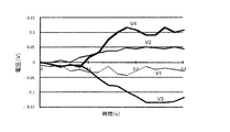
- FIG. 5 shows a voltage measurement value when the rubber-like elastic body 13 is eliminated and the space between the base 14 and the piezoelectric sheet 12 is a minute space. That is, a measured value is shown in which the voltage generated in each of the electrode portions 2a to 2b is measured over time when an amplifier is connected to each of the electrode portions 2a to 2d and the position 10 is pressed.
- V1 is a voltage generated in the electrode portion 2a
- V2 is a voltage generated in the electrode portion 2b
- V3 is a voltage generated in the electrode portion 2c
- V4 is a voltage generated in the electrode portion 2d.
- V1 is a positive voltage
- V2 is a voltage generated in the electrode portion 2b
- V3 is a voltage generated in the electrode portion 2c
- V4 is a voltage generated in the electrode portion 2d.
- FIG. 6 shows the same measurement result when the touch panel 1 has a structure in which the rubber-like elastic body 13 is inserted between the base 14 and the piezoelectric sheet 12 as shown in FIG.
- the piezoelectric sheet 12 is fixed to the base 14 via a rubber-like elastic body 13. That is, since the piezoelectric sheet 12 is not directly rigidly fixed to the base 14, the piezoelectric sheet 12 has a degree of freedom and can be vibrated. Since the protective film 11 is attached to the piezoelectric sheet 12, it has a unimorph structure, and the touch panel 1 itself can be vibrated by applying a signal voltage to each of the electrode portions 2a to 2d.
- FIG. 7 shows the result of calculating the fundamental vibration mode of the piezoelectric sheet 12 when a signal voltage is applied as described above by a finite element method simulation.
- the same signal is given to the electrode part 2a and the electrode part 2c, and a voltage having a polarity opposite to that of the signal given to the electrode parts 2a and 2c is given to the electrode parts 2b and 2d. Can be vibrated.
- FIG. 8 schematically shows the circuit configuration of the input / output device 5 configured using the touch panel 1 described above.
- the input / output device 5 includes a touch panel 1, a relay 20, an amplifier 21, an amplifier 22, a control module 23, a control line 30, an operation signal line 31, a drive signal line 32, and an input / output signal line 33.
- control module 23 a CPU, a memory, a music driving IC, a signal generator, and the like are incorporated as necessary.
- control module 23 When operating the touch panel 1 as an original input means, the control module 23 operates the relay 20 to connect the input / output signal line 33, the amplifier 21, and the operation signal line 31. The amplifier 22 is disconnected.
- a minute operation signal generated by pressing the touch panel 1 is amplified by the amplifier 21, the signal is analyzed by the control module 23, and position detection and pressure detection are performed.
- the control module 23 when operating the touch panel 1 as an output means, for example, when functioning as a tactile feedback device or a speaker, the control module 23 operates the relay 20 to connect the input / output signal line 33, the amplifier 22 and the drive signal line 32. Connecting. The amplifier 21 is disconnected.
- an AC signal as a drive signal output from the control module 23 is amplified by the amplifier 22 and sent to the touch panel 1 through the input / output signal line 33, and the touch panel 1 vibrates.
- control module 32 When outputting tactile feedback, the control module 32 immediately operates the relay 20 to return the touch panel 1 to the original input means.
- the touch panel 1 When functioning as a speaker, the touch panel 1 can be returned to the input means after a certain period of time or by operating a switch provided elsewhere.
- the function as a touch panel as an original input means, the function as a speaker (buzzer), and the function as a tactile feedback (haptics) 3 It can serve two functions.
- the division mode of the divided electrode that can be adopted in the present invention is not limited to four divisions as shown in FIG. 3 or FIG. Two or three divisions may be used, or five or more divisions may be used. Further, it is not necessary for all of the divided electrode portions to have a symmetrical shape, and the shapes may be different from each other.
- the number of divisions of the divided electrodes does not determine the number of detectable positions. That is, in the touch panel, two divisions are not necessary for detection of two locations, four divisions are necessary for detection of four locations, and 16 divisions are not necessary for detection of 16 locations. In principle, if the divided electrode is divided into two or more, an infinite position can be detected. However, with a small number of divisions such as two divisions or three divisions, the resolution tends to be poor.
- FIGS. 9 and 10 are views corresponding to FIG. 4 showing the second and third embodiments of the present invention, respectively. 9 and 10 show a split electrode divided into two so as to have two electrode portions 41 and 42.
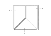
- FIG. 11 and FIG. 12 are diagrams corresponding to FIG. 4 showing the fourth and fifth embodiments of the present invention, respectively.
- FIG. 11 and FIG. 12 show a divided electrode that is divided into three so as to have three electrode portions 43 to 45.
- the number of divided electrodes is smaller than that of the four-divided one, it can be easily configured.
- the detection algorithm of the touch panel is greatly simplified.
- the position detection accuracy is reduced accordingly, it is useful as a touch panel that requires only rough position accuracy.
- the direction in which the dividing line of the dividing electrode is inserted and the shape of each electrode portion are determined based on the direction of the extending axis of the piezoelectric sheet, the outer shape of the piezoelectric sheet, and the like.
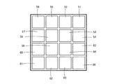
- FIG. 13 is a view corresponding to FIG. 4, showing a sixth embodiment of the present invention.
- FIG. 13 shows divided electrodes that are divided into 16 so as to have 16 electrode portions 51 to 66.
- the divided electrode shown in FIG. 13 corresponds to a further fine division of the four divisions in the first embodiment.
- the hatched electrode portions 55 to 58 and 63 to 66 are driven by a common signal, If the electrode portions 51 to 54 and 59 to 62 that are not hatched are driven to have a reverse voltage, vibration similar to that shown in FIG. 7 can be formed.
- FIG. 16 shows a simulation of the state of vibration when a vibration signal is given only to the hatched electrode portions 55 to 58 in FIG. 15 by the finite element method.
- the electrode portions 55 and 57 and the electrode portions 56 and 58 have different hatching directions. This is because the electrode portions 55 and 57 and the electrode portions 56 and 58 have different hatching directions. It is shown that voltages opposite to each other are applied. Note that no voltage is applied to the electrode portions 51 to 54 and 59 to 66 which are not hatched.
- a rubber-like elastic body different from the rubber-like elastic body 13 is added between the protective film 11 on the surface and the piezoelectric sheet 12. Also good. In this case, the soft feeling when touched is increased. Furthermore, in the experiments of the present inventors, it has been found that the output value of the voltage is further stabilized. However, in this case, in order to produce the unimorph effect, it is preferable to make the thicknesses of the rubber-like elastic bodies above and below the piezoelectric sheet 12 different from each other or to slightly increase the elastic modulus on one side.
- the voltage due to the electrostatic effect generated between the finger and the electrode 2 (for example, the principle of the electrostatic touch panel) is generated simultaneously with the generation of the voltage due to the piezoelectricity of the piezoelectric sheet 12.
- the same may be included as noise.
- the protective film 11 has a two-layer structure, and a uniform transparent electrode is formed at the interface between the two-layer structure in the protective film 11, and if this is grounded, such noise is removed. be able to.
- the piezoelectric sheet 12 is made of PLLA, stable piezoelectric characteristics can be obtained and excellent transparency can be obtained.
- a chiral polymer other than PLLA may be used as the material of the piezoelectric sheet 12.
- poly- ⁇ -methyl-L-glutamate or poly- ⁇ -benzyl-L-glutamate can be used as the material for the piezoelectric sheet 12. Since the piezoelectric constant of such a material is d 14 , positive and negative voltages can be obtained as a touch panel as described above. Therefore, it can be used very advantageously as sensing. If accuracy and transparency can be sacrificed somewhat, polyvinylidene fluoride can be used as the piezoelectric body.
- the touch panel 1 may not need to be transparent depending on the application.
- all or any of the protective film 11, the piezoelectric sheet 12, the electrode including the first electrode 2, the rubber-like elastic body 13, and the base 14 may be opaque.
Abstract
押圧操作位置および押圧力の検知が可能であるとともに、操作者に対して音や触覚を与えることができ、しかも、厚みの薄いタッチパネルを実現する。 より小さい厚み寸法とするため、たとえば所定の方向に向く延伸軸を有するL型ポリ乳酸シートからなる圧電シート(12)と、圧電シート(12)の第1および第2の主面上にそれぞれ形成された第1および第2の電極と、圧電シート(12)の第1の主面側に貼り付けられ、操作者による押圧操作が及ぼされるべき操作面を構成する保護フィルム(11)と、圧電シート(12)の第2の主面側に配置された基体(14)とを備える構成とされ、第1および第2の電極の少なくとも一方は、互いに電気的に絶縁された複数の電極部分を有する分割電極とされる。さらに、押圧操作位置の検出精度を高めるため、圧電シート(12)と基体(14)との間にゴム状弾性体(13)が配置される。
Description
この発明は、タッチパネル、およびこのタッチパネルを用いて構成される入出力装置に関するもので、特に、タッチパネルの押圧操作位置についての検出精度の向上を図るための技術に関するものである。
この発明にとって興味あるタッチパネルが、たとえば特開平11-212725号公報(特許文献1)に記載されている。特許文献1の特に図3には、現金自動出納機に備える情報表示装置における表示操作部が図示されている。この表示操作部は、窓を有するケース内に液晶表示パネルを収容しており、液晶表示パネルの主面が情報表示面となっている。液晶表示パネルの情報表示面に対して平行にかつ所定の間隔を隔てて、操作パネルが配置される。液晶表示パネルの4隅の各近傍であって、上記ケースの底面には、圧電素子が配置され、操作パネルは、これら圧電素子によって支持されている。
特許文献1に記載のタッチパネルでは、操作パネルの操作面のいずれの位置を押圧操作したかが、4個の圧電素子を用いて検知され、また、操作パネルの操作面を押圧操作した操作者に対して、圧電素子が振動を与えることにより、操作感を与えるようにしている。
しかしながら、特許文献1に記載のタッチパネルでは、圧電素子が比較的大きな厚み寸法を占めるため、タッチパネルの厚みを薄くすることが困難である。
そこで、この発明の目的は、上述したような問題を解決し得るタッチパネル、およびそれを用いて構成される入出力装置を提供しようとすることである。
この発明に係るタッチパネルは、より小さい厚み寸法とするため、圧電性を有する圧電シートと、圧電シートの互いに対向する第1および第2の主面上にそれぞれ形成された、互いに対向する第1および第2の電極と、圧電シートの第1の主面側に貼り付けられ、操作者による押圧操作が及ぼされるべき操作面を構成する保護フィルムと、圧電シートの第2の主面側に配置された基体とを備える構成とされる。ここで、第1および第2の電極の少なくとも一方は、互いに電気的に絶縁された複数の電極部分を有する分割電極とされる。さらに、押圧操作位置の検出精度を高めるため、圧電シートと基体との間にゴム状弾性体が配置される。
上記圧電シートは、所定の方向に向く延伸軸を有するL型ポリ乳酸シートであることが好ましい。
また、この発明に係るタッチパネルにおいて、圧電シート、第1および第2の電極、保護フィルムならびにゴム状弾性体は透明性を有することが好ましい。
この発明は、また、上述したタッチパネルを備える、入出力装置にも向けられる。この発明に係る入出力装置は、操作面上の任意の位置への押圧操作に応じて分割電極の複数の電極部分の各々から出力される電気信号を操作信号として取り出す操作信号取出し手段と、操作信号に応答して分割電極の複数の電極部分の各々に駆動信号をフィードバックする駆動信号フィードバック手段とを備えている。
この発明に係る入出力装置において、タッチパネルは、駆動信号により操作者に対して音を発するようにされても、操作者に対して触覚を与えるようにされても、これら両者が実行されるようにされてもよい。
この発明によれば、押圧操作位置の検知および押圧力の検知といった3次元的な押圧操作情報を取得することができるとともに、圧電シート自体によって、操作者に対して、音や触覚を与えることができ、そして、このような多機能を有するにも関わらず、厚み寸法の小さいタッチパネルを実現することができる。
また、この発明に係るタッチパネルによれば、圧電シートと基体との間にゴム状弾性体が配置されるので、押圧操作位置の検出精度を高めることができる。
この発明に係るタッチパネルにおいて、圧電シート、第1および第2の電極、保護フィルム、ならびにゴム状弾性体が透明性を有していると、基体をたとえばフラットパネルディスプレイで構成したり、基体をも透明性を有する構成としながら、その下にフラットパネルディスプレイを配置したりすることにより、フラットパネルディスプレイを見ながらの押圧操作が可能となる。
図1に、この発明の第1の実施形態によるタッチパネル1の外観が斜視図で示されている。このタッチパネル1の断面図が図2に示されている。
タッチパネル1は、図2に示すように、保護フィルム11、圧電シート12、ゴム状弾性体13、および基体14がこの順で積層された断面構造を有している。タッチパネル1は、通常、液晶ディスプレイや有機ELディスプレイ等のフラットパネルディスプレイ(FPD)の表面に配置される。よって、タッチパネル1を構成する各要素は、好ましくは、透明性を有する材料から構成される。保護フィルム11は、操作者による押圧操作が及ぼされるべき操作面を構成するもので、その表面には、図示を省略するが、反射防止膜や傷防止や汚れ防止のためハードコートが施される場合がある。
図3に、圧電シート12が斜視図で示されている。圧電シート12は、好ましくは、L型ポリ乳酸(PLLA)から構成される。PLLAからなる圧電シート12は、延伸されかつ熱処理されることにより圧電性が与えられるものであり、この実施形態では、矢印の方向に向く延伸軸15を有している。
図3において、電極2が図示されているが、圧電シート12の互いに対向する第1および第2の主面上には、それぞれ、互いに対向する第1および第2の電極が形成される。これら電極は、好ましくは、酸化インジウム錫、酸化インジウム亜鉛、酸化亜鉛、ポリチオフェン系導電性ポリマー、アニリン系導電性ポリマーのような透明性を有する材料から構成される。電極が、酸化インジウム錫や酸化インジウム亜鉛、酸化亜鉛のような無機材料から構成される場合には、たとえばスパッタリングによる形成方法が適用され、ポリチオフェン系導電性ポリマーやアニリン系導電性ポリマーのような有機材料から構成される場合には、塗布による形成方法が適用される。
第1および第2の電極の少なくとも一方は、互いに電気的に絶縁された複数の電極部分を有する分割電極とされる。図3および図4には、圧電シート12の第1の主面12a側が図示されている。この第1の主面12aは、図2において、上側に向く主面であっても、下側に向く面であってもよい。この第1の主面12a上には、第1の電極2が形成され、第1の電極2は、たとえば4個の電極部分2a~2dを有する分割電極とされている。図示されない第2の主面上に形成される第2の電極については、第1の電極2と同様、4個の電極部分を有する分割電極とされても、第1の電極2の4個の電極部分2a~2dに共通に対向する一様な電極とされてもよい。
保護フィルム11は、たとえばポリエチレンテレフタレートまたはポリエチレンナフタレートから構成される。また、基体14についても、たとえばポリエチレンテレフタレートまたはポリエチレンナフタレートから構成されるが、これに代えて、FPDによって与えられてもよい。保護フィルム11は、好ましくは、基体14よりも薄くされる。
ゴム状弾性体13は、ゴム状態であり、ゴム弾性(エントロピー弾性)を有する弾性体である。ゴム状弾性体13を構成する材料としては、たとえばポリウレタンゴム、シリコーンゴムのような高透明度のものが好適であり、また、硬度Hs20~50のものが好適である。用いられるゴムの厚さ、種類および硬度については、保護フィルム11の厚さおよび硬さ、圧電シート12の厚さ、圧電定数および検知精度等を鑑みて決定される設計事項である。
圧電シート12の任意の位置が押圧されて変形すると、電極部分2a~2dの各々に所定の電圧が発生する。この電圧の情報を元に押圧操作された平面的な位置と押圧力とを検知することができる。
すなわち、押圧操作に応じて電極部分2a~2dの各々に発生する電圧から得られる電圧情報を予め記憶しておき、この記憶された電圧情報と実際に検出された電極部分2a~2dの各々に発生する電圧から得られた電圧情報とを比較することによって、押圧操作された位置と押圧力とを検知することができる。
このような押圧操作の位置および押圧力の検出精度の向上にゴム状弾性体13が寄与している。これについて以下に説明する。
図4は、図3に示した圧電シート12を第1の主面12a側から示した平面図である。なお、図3および図4において、電極からの引き出し線の図示は省略されている。
圧電シート12は変形することにより電圧を生じる。したがって、基体14と圧電シート12との間に微小な空隙を設けた場合にも、圧電シート12に電圧を生じさせることができる。
圧電シート12の延伸軸15は、前述したように、図4に矢印で示した方向とされている。電極部分2a~2dは、圧電シート12を同じ形状で均等に4分割された領域にそれぞれ形成されている。このような分割状態においては、この圧電シート12上の円で示した位置10に応力を与えたときに生じる電圧は、電極部分2cと電極部分2dとで、ほぼ絶対値が互いに等しくかつ逆極性の電圧が観測され、電極部分2aと電極部分2bとで、ほぼ絶対値が互いに等しくかつ逆極性の電圧が観測されるはずである。また、電極部分2aおよび2bの各々で観測される電圧の絶対値は、電極部分2cおよび2dの各々で観測される電圧の絶対値よりも大分小さくなるはずである。有限要素法のシミュレーションでも、これと同様の結果が得られる。
図5は、ゴム状弾性体13を無くし、基体14と圧電シート12との間が微小な空間とされている場合の電圧測定値を表わしたものである。すなわち、電極部分2a~2dの各々にアンプを接続し、位置10を押したとき、電極部分2a~2bの各々に発生する電圧を時間の経過とともに測定した測定値が示されている。
図5において、V1は電極部分2aに発生する電圧、V2は電極部分2bに発生する電圧、V3は電極部分2cに発生する電圧、V4は電極部分2dに発生する電圧である。図5からわかるように、V1のみが正の電圧となり、V2、V3およびV4は、すべて負の電圧であり、それらの差もそれほど大きくない。このように、図5に示した結果は、先に予測したとおりの値にはなっていないことがわかる。
一方、タッチパネル1を、図2に示すとおり、基体14と圧電シート12との間にゴム状弾性体13を入れた構造としたときの同様の測定結果が図6に示されている。
図6では、V1~V4の関係は、先に予測したものに完全に合致していることがわかる。したがって、タッチパネル1を図2に示すような構造とすれば、シミュレーションに合致した測定結果が得られる。このことから、図2に示すような構造のタッチパネル1によれば、位置と押圧力の双方を検知し得ることがわかる。
図2に示した構造では、圧電シート12がゴム状弾性体13を介して基体14に固定されている。すなわち、圧電シート12は、基体14に対して、直接リジッドに固定されていないため、圧電シート12には自由度があり、これを振動させることが可能である。圧電シート12には保護フィルム11が貼り付けられているため、ユニモルフ構造となっており、電極部分2a~2dの各々に信号電圧を与えることによりタッチパネル1自体を振動させることができる。
図7は、上述のように信号電圧を与えたときの圧電シート12の基本振動モードを有限要素法シミュレーションにより計算した結果を示したものである。この実施形態では、電極部分2aと電極部分2cとに互いに同じ信号を与え、電極部分2bおよび2dに、電極部分2aおよび2cに与えられている信号と逆極性の電圧を与えることにより、このような振動を起こさせることができる。
この場合、音声信号を与えれば音楽を鳴らすことができ、指の触覚に適した周波数の信号を入れることによって触覚をフィードバック(ハプティクス)することができる。
図8は、上述したタッチパネル1を用いて構成される入出力装置5の回路構成を略図的に示したものである。
入出力装置5は、タッチパネル1、リレー20、アンプ21、アンプ22、制御モジュール23、制御ライン30、操作信号線31、駆動信号線32および入出力信号線33を備えている。
制御モジュール23には、CPU、メモリ、音楽駆動IC、信号発生器などが必要に応じて組み込まれている。
タッチパネル1を本来の入力手段として動作させるときは、制御モジュール23はリレー20を操作して、入出力信号線33とアンプ21および操作信号線31とを接続する。アンプ22は切り離される。
この状態で、タッチパネル1を押圧操作したことにより発生する微小な操作信号はアンプ21で増幅されて、制御モジュール23で信号が解析され、位置検知および押圧力検知が行なわれる。
他方、タッチパネル1を出力手段として動作させるとき、たとえば触覚フィードバック装置もしくはスピーカとして機能させるときは、制御モジュール23はリレー20を操作して、入出力信号線33とアンプ22および駆動信号線32とを接続する。アンプ21は切り離される。
この状態で、制御モジュール23から出された駆動信号としての交流信号はアンプ22で増幅されて、入出力信号線33を通じてタッチパネル1に送られ、タッチパネル1が振動する。
触覚フィードバックの際は1ショットの信号を出力した後、制御モジュール32はすぐにリレー20を操作してタッチパネル1が本来の入力手段に復帰する。
スピーカとして機能させた際は、一定時間後、もしくは他に設けられたスイッチの操作により、タッチパネル1が入力手段へと復帰させることができる。
触覚フィードバックの直後もしくは直前に「ポン」というような音を出すような動作をさせてもよい。このようにすることにより、音と触覚により操作感を確実に得ることができる。
このように、タッチパネル1によれば、1枚のフィルム状のデバイスでありながら、本来の入力手段としてのタッチパネルとしての機能、スピーカ(ブザー)としての機能および触覚フィードバック(ハプティクス)としての機能といった3つの機能を果たすことができる。
この発明において採用され得る分割電極の分割態様としては、図3または図4に示したような4分割に限らない。2分割または3分割でもよく、あるいは5分割以上でもよい。また、分割された電極部分は、すべて対称形状とする必要はなく、互いに形状が異なっていてもよい。
ここで注意すべきは、分割電極の分割数が検出可能な位置の数を決めるものではないということである。すなわち、タッチパネルにおいて、2箇所の検出のためには2分割、4箇所の検出のためには4分割、16箇所の検出のためには16分割がそれぞれ必要ということではない。原理的には、分割電極が2分割以上なら、無限の位置を検出することができる。ただ、2分割や3分割といった少ない分割数では、分解能が悪くなりがちであるというにすぎない。
以下に、図面を参照しながら、他の分割態様の具体例について説明する。
図9および図10は、それぞれ、この発明の第2および第3の実施形態を示す、図4に対応する図である。図9および図10には、2個の電極部分41および42を有するように2分割された分割電極が示されている。
図11および図12は、それぞれ、この発明の第4および第5の実施形態を示す、図4に対応する図である。図11および図12には、3個の電極部分43~45を有するように3分割された分割電極が示されている。
これら第2ないし第5の実施形態によれば、4分割のものに比べて、分割電極の分割数が少ないため、簡単に構成することができる。また、情報量が少ないため、タッチパネルの検知アルゴリズムは非常に簡素化される。ただし、その分、位置の検出精度は低下するが、ラフな位置精度しか要求されないタッチパネルとしては有用である。これら第2ないし第5の実施形態でも、音を鳴らしたり、触覚フィードバック用の振動を生じさせたりすることができるが、4分割と比較して変位量は小さくなる傾向がある。分割電極の分割線をどの方向に入れるか、各電極部分の形状をどのようにするかは、圧電シートの延伸軸の方向、圧電シートの外形等に基づいて決定される設計事項である。
図13は、この発明の第6の実施形態を示す、図4に対応する図である。図13には、16個の電極部分51~66を有するように16分割された分割電極が示されている。図13に示した分割電極は、第1の実施形態での4分割をさらに細かく分割したものに相当する。
図13に示した実施形態に係るタッチパネルを動作させるに際して、すべての電極部分51~66から独立して電圧を検出すれば、より精度の高い位置検出や押圧力検出が可能となる。位置情報の計算の際には得られた電圧の絶対値に対して閾値を設けておき、所定の電圧以下のデータを使わないようにすれば、計算量の増大は緩和できる。
図13に示した実施形態に係るタッチパネルをスピーカまたは触覚フィードバックとして駆動する際には、図14に示すように、ハッチングを施した電極部分55~58および63~66を共通の信号で駆動し、ハッチングを施していない電極部分51~54および59~62を逆電圧となるように駆動すれば、図7に示した振動と同じような振動を形成することができる。
また、触覚フィードバックに際して、触れられた部分の近傍の4個の電極部分を使用して振動を与えれば、タッチパネル全体が震えるのではなく、触れた部分の近傍で触覚フィードバックが得られるタッチパネルとすることができる。このことを、図15および図16を参照して説明する。
図15においてハッチングを施した電極部分55~58にのみ振動信号を与えたときの振動の様子を有限要素法でシミュレーションしたものが図16に示されている。図15においてハッチングを施した電極部分55~58のうち、電極部分55および57と電極部分56および58とでハッチングの向きが異なっているが、これは電極部分55および57と電極部分56および58とで互いに逆の電圧が印加されていることを示している。なお、ハッチングを施していない電極部分51~54および59~66には電圧が印加されていない。
この発明のさらに他の実施形態として、図2を参照して説明すると、表面の保護フィルム11と圧電シート12との間に、ゴム状弾性体13とは別のゴム状弾性体を追加してもよい。この場合、触ったときのソフト感が増す。さらに、本件発明者らの実験では、電圧の出力値がさらに安定するという知見が得られている。ただし、この場合、ユニモルフ効果を出すためには、圧電シート12の上下にあるゴム状弾性体の厚みを互いに異ならせるか、一方側の弾性率をやや高くすることが好適である。
また、図2に示すような構造のタッチパネル1では、圧電シート12の圧電性による電圧の発生と同時に、たとえば指と電極2との間に生じる静電効果による電圧(静電式タッチパネルの原理と同じ)がノイズとして含まれる可能性がある。これに対しては、保護フィルム11を2層構造とし、保護フィルム11における2層構造間の界面に一様な透明電極を形成し、これを接地しておけば、このようなノイズを除去することができる。
また、圧電シート12をPLLAから構成すると、安定した圧電特性を得ることができるとともに、透明性に優れたものとすることができる。しかしながら、このような利点を特に望まないならば、PLLA以外のキラル高分子を圧電シート12の材料として用いてもよい。たとえば、ポリ-γ-メチル-L-グルタメートやポリ-γ-ベンジル-L-グルタメートを、圧電シート12の材料として用いることができる。このような材料の圧電定数はd14であるため、これまで説明してきたようにタッチパネルとして正負の電圧が得られる。したがって、センシングとして非常に有利に用いることができる。精度、透明度が幾分、犠牲にできる場合はポリフッ化ビニリデンを圧電体として用いることができる。
また、タッチパネル1は、その用途によっては、透明性を有している必要がないこともある。この場合には、たとえば、保護フィルム11、圧電シート12、第1の電極2を含む電極、ゴム状弾性体13および基体14のすべてまたはいずれかは、不透明とされてもよい。
1 タッチパネル
2 第1の電極
2a~2d,41,42,43~45,51~66 電極部分
5 入出力装置
11 保護フィルム
12 圧電シート
12a 第1の主面
13 ゴム状弾性体
14 基体
15 延伸軸
20 リレー
23 制御モジュール
30 制御ライン
31 操作信号線
32 駆動信号線
33 入出力信号線
2 第1の電極
2a~2d,41,42,43~45,51~66 電極部分
5 入出力装置
11 保護フィルム
12 圧電シート
12a 第1の主面
13 ゴム状弾性体
14 基体
15 延伸軸
20 リレー
23 制御モジュール
30 制御ライン
31 操作信号線
32 駆動信号線
33 入出力信号線
Claims (6)
- 圧電性を有する圧電シートと、
前記圧電シートの互いに対向する第1および第2の主面上にそれぞれ形成された、互いに対向する第1および第2の電極と、
前記圧電シートの前記第1の主面側に貼り付けられ、操作者による押圧操作が及ぼされるべき操作面を構成する保護フィルムと、
前記圧電シートの前記第2の主面側に配置された基体と
を備え、
前記第1および第2の電極の少なくとも一方は、互いに電気的に絶縁された複数の電極部分を有する分割電極とされ、さらに、
前記圧電シートと前記基体との間に配置されたゴム状弾性体を備える、
タッチパネル。 - 前記圧電シートは、所定の方向に向く延伸軸を有するL型ポリ乳酸シートである、請求項1に記載のタッチパネル。
- 前記圧電シート、前記第1および第2の電極、前記保護フィルムならびに前記ゴム状弾性体は透明性を有する、請求項1または2に記載のタッチパネル。
- 請求項1ないし3のいずれかに記載のタッチパネルを備える、入出力装置であって、
前記操作面上の任意の位置への押圧操作に応じて前記分割電極の複数の前記電極部分の各々から出力される電気信号を操作信号として取り出す操作信号取出し手段と、
前記操作信号に応答して前記分割電極の複数の前記電極部分の各々に駆動信号をフィードバックする駆動信号フィードバック手段と
を備える、入出力装置。 - 前記タッチパネルは、前記駆動信号により操作者に対して音を発する、請求項4に記載の入出力装置。
- 前記タッチパネルは、前記駆動信号により操作者に対して触覚を与える、請求項4または5に記載の入出力装置。
Applications Claiming Priority (2)
| Application Number | Priority Date | Filing Date | Title |
|---|---|---|---|
| JP2010-090203 | 2010-04-09 | ||
| JP2010090203 | 2010-04-09 |
Publications (1)
| Publication Number | Publication Date |
|---|---|
| WO2011125408A1 true WO2011125408A1 (ja) | 2011-10-13 |
Family
ID=44762369
Family Applications (1)
| Application Number | Title | Priority Date | Filing Date |
|---|---|---|---|
| PCT/JP2011/055611 WO2011125408A1 (ja) | 2010-04-09 | 2011-03-10 | タッチパネルおよびタッチパネルを備える入出力装置 |
Country Status (1)
| Country | Link |
|---|---|
| WO (1) | WO2011125408A1 (ja) |
Cited By (26)
| Publication number | Priority date | Publication date | Assignee | Title |
|---|---|---|---|---|
| JP2013131110A (ja) * | 2011-12-22 | 2013-07-04 | Kddi Corp | タッチパネル、電話機 |
| US20140049137A1 (en) * | 2011-04-08 | 2014-02-20 | Murata Manufacturing Co., Ltd. | Displacement Sensor, Displacement Detecting Device, and Operation Device |
| WO2014119476A1 (ja) * | 2013-02-01 | 2014-08-07 | 株式会社村田製作所 | 押圧センサ付き表示パネル、および押圧入力機能付き電子機器 |
| WO2014117724A1 (zh) * | 2013-01-29 | 2014-08-07 | 中国科学院苏州纳米技术与纳米仿生研究所 | 电子皮肤及其制备方法和应用 |
| WO2014119475A1 (ja) * | 2013-02-01 | 2014-08-07 | 株式会社村田製作所 | 押圧センサ付き表示パネル、および押圧入力機能付き電子機器 |
| JP2014194591A (ja) * | 2013-03-28 | 2014-10-09 | Fujitsu Ltd | 検出装置、検出方法および電子機器 |
| WO2014185530A1 (ja) | 2013-05-16 | 2014-11-20 | 三井化学株式会社 | 押圧検出装置及びタッチパネル |
| WO2014192541A1 (ja) * | 2013-05-27 | 2014-12-04 | 株式会社村田製作所 | 押圧センサ付き表示パネル、および押圧入力機能付き電子機器 |
| WO2015019981A1 (ja) * | 2013-08-06 | 2015-02-12 | 株式会社村田製作所 | 押圧検出センサ |
| WO2015050096A1 (ja) * | 2013-10-04 | 2015-04-09 | 株式会社村田製作所 | 携帯装置、および、認証プログラム |
| WO2015053089A1 (ja) | 2013-10-07 | 2015-04-16 | 三井化学株式会社 | 押圧検出装置及び押圧検出タッチパネル |
| CN104660892A (zh) * | 2013-11-19 | 2015-05-27 | 奥林巴斯株式会社 | 操作装置 |
| JP2015110312A (ja) * | 2013-10-29 | 2015-06-18 | ダイキン工業株式会社 | 積層体 |
| WO2015107932A1 (ja) * | 2014-01-20 | 2015-07-23 | 株式会社村田製作所 | 圧電センサ |
| JP2015215734A (ja) * | 2014-05-09 | 2015-12-03 | 日東電工株式会社 | タッチパネル用シートセンサー |
| US20150362647A1 (en) * | 2013-02-01 | 2015-12-17 | Murata Manufacturing Co., Ltd. | Display device and laminated optical film |
| WO2015194446A1 (ja) * | 2014-06-20 | 2015-12-23 | 株式会社村田製作所 | タッチパネル、および入力操作端末 |
| US20160099403A1 (en) * | 2013-04-10 | 2016-04-07 | Mitsui Chemicals, Inc. | Layered body |
| US20160204337A1 (en) * | 2013-09-02 | 2016-07-14 | Mitsui Chemicals, Inc. | Layered body |
| WO2016121218A1 (ja) * | 2015-01-28 | 2016-08-04 | 株式会社村田製作所 | ネットワーク認証システム、端末、ネットワーク機構、プログラム、および、ネットワーク認証方法 |
| JP6020745B2 (ja) * | 2014-04-07 | 2016-11-02 | 株式会社村田製作所 | タッチセンサ |
| WO2018048648A1 (en) * | 2016-09-08 | 2018-03-15 | Microsoft Technology Licensing, Llc | Display structure having a visual display and an audio output |
| CN110134283A (zh) * | 2013-10-28 | 2019-08-16 | 苹果公司 | 基于压电的力感测 |
| JP2020119995A (ja) * | 2019-01-23 | 2020-08-06 | 味の素株式会社 | 圧電シートおよびその製造方法 |
| WO2020179376A1 (ja) * | 2019-03-06 | 2020-09-10 | 日東電工株式会社 | センサー装置 |
| WO2021053998A1 (ja) * | 2019-09-20 | 2021-03-25 | 株式会社ジャパンディスプレイ | 触覚装置 |
Citations (4)
| Publication number | Priority date | Publication date | Assignee | Title |
|---|---|---|---|---|
| JP2004125571A (ja) * | 2002-10-01 | 2004-04-22 | National Institute Of Advanced Industrial & Technology | 透明圧電センサおよびそれを備えた入力装置 |
| WO2009144964A1 (ja) * | 2008-05-29 | 2009-12-03 | 株式会社村田製作所 | 圧電スピーカ、スピーカ装置およびタクタイルフィードバック装置 |
| WO2010038466A1 (ja) * | 2008-10-03 | 2010-04-08 | ダイキン工業株式会社 | タッチパネルおよび透明圧電シート |
| WO2010143528A1 (ja) * | 2009-06-11 | 2010-12-16 | 株式会社村田製作所 | タッチパネルおよびタッチ式入力装置 |
-
2011
- 2011-03-10 WO PCT/JP2011/055611 patent/WO2011125408A1/ja active Application Filing
Patent Citations (4)
| Publication number | Priority date | Publication date | Assignee | Title |
|---|---|---|---|---|
| JP2004125571A (ja) * | 2002-10-01 | 2004-04-22 | National Institute Of Advanced Industrial & Technology | 透明圧電センサおよびそれを備えた入力装置 |
| WO2009144964A1 (ja) * | 2008-05-29 | 2009-12-03 | 株式会社村田製作所 | 圧電スピーカ、スピーカ装置およびタクタイルフィードバック装置 |
| WO2010038466A1 (ja) * | 2008-10-03 | 2010-04-08 | ダイキン工業株式会社 | タッチパネルおよび透明圧電シート |
| WO2010143528A1 (ja) * | 2009-06-11 | 2010-12-16 | 株式会社村田製作所 | タッチパネルおよびタッチ式入力装置 |
Cited By (54)
| Publication number | Priority date | Publication date | Assignee | Title |
|---|---|---|---|---|
| US11877516B2 (en) | 2011-04-08 | 2024-01-16 | Murata Manufacturing Co., Ltd. | Displacement sensor, displacement detecting device, and operation device |
| US20140049137A1 (en) * | 2011-04-08 | 2014-02-20 | Murata Manufacturing Co., Ltd. | Displacement Sensor, Displacement Detecting Device, and Operation Device |
| US9627605B2 (en) * | 2011-04-08 | 2017-04-18 | Murata Manufacturing Co., Ltd. | Displacement sensor having a piezoelectric layer comprising polylactic acid, displacement detecting device and operation device having the same |
| US10446738B2 (en) | 2011-04-08 | 2019-10-15 | Murata Manufacturing Co., Ltd. | Displacement sensor, displacement detecting device, and operation device |
| US11469364B2 (en) | 2011-04-08 | 2022-10-11 | Murata Manufacturing Co., Ltd. | Displacement sensor, displacement detecting device, and operation device |
| JP2013131110A (ja) * | 2011-12-22 | 2013-07-04 | Kddi Corp | タッチパネル、電話機 |
| WO2014117724A1 (zh) * | 2013-01-29 | 2014-08-07 | 中国科学院苏州纳米技术与纳米仿生研究所 | 电子皮肤及其制备方法和应用 |
| US9990072B2 (en) | 2013-02-01 | 2018-06-05 | Murata Manufacturing Co., Ltd. | Display panel with pressure sensor and electronic device with pressing input function |
| JP5860980B2 (ja) * | 2013-02-01 | 2016-02-16 | 株式会社村田製作所 | 押圧センサ付き表示パネル、および押圧入力機能付き電子機器 |
| WO2014119476A1 (ja) * | 2013-02-01 | 2014-08-07 | 株式会社村田製作所 | 押圧センサ付き表示パネル、および押圧入力機能付き電子機器 |
| US10928858B2 (en) | 2013-02-01 | 2021-02-23 | Murata Manufacturing Co., Ltd. | Display panel with pressing sensor and electronic device with pressing input function |
| CN104981759B (zh) * | 2013-02-01 | 2018-03-13 | 株式会社村田制作所 | 带按压传感器的显示面板及带按压输入功能的电子设备 |
| WO2014119475A1 (ja) * | 2013-02-01 | 2014-08-07 | 株式会社村田製作所 | 押圧センサ付き表示パネル、および押圧入力機能付き電子機器 |
| US10126473B2 (en) * | 2013-02-01 | 2018-11-13 | Murata Manufacturing Co., Ltd. | Display device and laminated optical film |
| CN104981759A (zh) * | 2013-02-01 | 2015-10-14 | 株式会社村田制作所 | 带按压传感器的显示面板及带按压输入功能的电子设备 |
| JP5939319B2 (ja) * | 2013-02-01 | 2016-06-22 | 株式会社村田製作所 | 押圧センサ付き表示パネル、および押圧入力機能付き電子機器 |
| US20150362647A1 (en) * | 2013-02-01 | 2015-12-17 | Murata Manufacturing Co., Ltd. | Display device and laminated optical film |
| JPWO2014119475A1 (ja) * | 2013-02-01 | 2017-01-26 | 株式会社村田製作所 | 押圧センサ付き表示パネル、および押圧入力機能付き電子機器 |
| JP2014194591A (ja) * | 2013-03-28 | 2014-10-09 | Fujitsu Ltd | 検出装置、検出方法および電子機器 |
| US20160099403A1 (en) * | 2013-04-10 | 2016-04-07 | Mitsui Chemicals, Inc. | Layered body |
| US10031606B2 (en) | 2013-05-16 | 2018-07-24 | Mitsui Chemicals, Inc. | Pressure detecting device and touch panel |
| WO2014185530A1 (ja) | 2013-05-16 | 2014-11-20 | 三井化学株式会社 | 押圧検出装置及びタッチパネル |
| WO2014192541A1 (ja) * | 2013-05-27 | 2014-12-04 | 株式会社村田製作所 | 押圧センサ付き表示パネル、および押圧入力機能付き電子機器 |
| US10503305B2 (en) | 2013-05-27 | 2019-12-10 | Murata Manufacturing Co., Ltd. | Display panel with pressure sensor and electronic device with pressing input function |
| JP6069500B2 (ja) * | 2013-05-27 | 2017-02-01 | 株式会社村田製作所 | 押圧センサ付き表示パネル、および押圧入力機能付き電子機器 |
| US10146352B2 (en) | 2013-08-06 | 2018-12-04 | Murata Manufacturing Co., Ltd. | Pressure-detecting sensor |
| WO2015019981A1 (ja) * | 2013-08-06 | 2015-02-12 | 株式会社村田製作所 | 押圧検出センサ |
| US20160204337A1 (en) * | 2013-09-02 | 2016-07-14 | Mitsui Chemicals, Inc. | Layered body |
| WO2015050096A1 (ja) * | 2013-10-04 | 2015-04-09 | 株式会社村田製作所 | 携帯装置、および、認証プログラム |
| US9582654B2 (en) | 2013-10-04 | 2017-02-28 | Murata Manufacturing Co., Ltd. | Mobile device, and authentication program |
| JPWO2015050096A1 (ja) * | 2013-10-04 | 2017-03-09 | 株式会社村田製作所 | 携帯装置、および、認証プログラム |
| US10190924B2 (en) | 2013-10-07 | 2019-01-29 | Murata Manufacturing Co., Ltd. | Pressure-sensing device and pressure-sensing touch panel |
| WO2015053089A1 (ja) | 2013-10-07 | 2015-04-16 | 三井化学株式会社 | 押圧検出装置及び押圧検出タッチパネル |
| CN110134283A (zh) * | 2013-10-28 | 2019-08-16 | 苹果公司 | 基于压电的力感测 |
| JP2015110312A (ja) * | 2013-10-29 | 2015-06-18 | ダイキン工業株式会社 | 積層体 |
| CN104660892A (zh) * | 2013-11-19 | 2015-05-27 | 奥林巴斯株式会社 | 操作装置 |
| JP2015099506A (ja) * | 2013-11-19 | 2015-05-28 | オリンパス株式会社 | 操作装置、表示装置及び撮像装置 |
| US10197460B2 (en) | 2014-01-20 | 2019-02-05 | Murata Manufacturing Co., Ltd. | Piezoelectric sensor including a sensor unit having a first adhesive layer with different properties than a second adhesive layer |
| WO2015107932A1 (ja) * | 2014-01-20 | 2015-07-23 | 株式会社村田製作所 | 圧電センサ |
| JP6052437B2 (ja) * | 2014-01-20 | 2016-12-27 | 株式会社村田製作所 | 圧電センサ |
| US9946388B2 (en) | 2014-04-07 | 2018-04-17 | Murata Manufacturing Co., Ltd. | Touch sensor with improved pressure sensing characteristics |
| JP6020745B2 (ja) * | 2014-04-07 | 2016-11-02 | 株式会社村田製作所 | タッチセンサ |
| JPWO2015156195A1 (ja) * | 2014-04-07 | 2017-04-13 | 株式会社村田製作所 | タッチセンサ |
| JP2015215734A (ja) * | 2014-05-09 | 2015-12-03 | 日東電工株式会社 | タッチパネル用シートセンサー |
| WO2015194446A1 (ja) * | 2014-06-20 | 2015-12-23 | 株式会社村田製作所 | タッチパネル、および入力操作端末 |
| CN106462277A (zh) * | 2014-06-20 | 2017-02-22 | 株式会社村田制作所 | 触摸面板以及输入操作终端 |
| WO2016121218A1 (ja) * | 2015-01-28 | 2016-08-04 | 株式会社村田製作所 | ネットワーク認証システム、端末、ネットワーク機構、プログラム、および、ネットワーク認証方法 |
| US10206044B2 (en) | 2016-09-08 | 2019-02-12 | Microsoft Technology Licensing, Llc | Display structure having a visual display and an audio output |
| WO2018048648A1 (en) * | 2016-09-08 | 2018-03-15 | Microsoft Technology Licensing, Llc | Display structure having a visual display and an audio output |
| JP2020119995A (ja) * | 2019-01-23 | 2020-08-06 | 味の素株式会社 | 圧電シートおよびその製造方法 |
| JP7280566B2 (ja) | 2019-01-23 | 2023-05-24 | 味の素株式会社 | 圧電シートおよびその製造方法 |
| JPWO2020179376A1 (ja) * | 2019-03-06 | 2020-09-10 | ||
| WO2020179376A1 (ja) * | 2019-03-06 | 2020-09-10 | 日東電工株式会社 | センサー装置 |
| WO2021053998A1 (ja) * | 2019-09-20 | 2021-03-25 | 株式会社ジャパンディスプレイ | 触覚装置 |
Similar Documents
| Publication | Publication Date | Title |
|---|---|---|
| WO2011125408A1 (ja) | タッチパネルおよびタッチパネルを備える入出力装置 | |
| US9727157B2 (en) | Touch sensitive device providing a tactile feedback, display device comprising the same and method of driving the same | |
| US10088936B2 (en) | Thin profile user interface device and method providing localized haptic response | |
| WO2011024434A1 (ja) | 触感呈示装置及び触感呈示装置の制御方法 | |
| US20070080951A1 (en) | Input device and electronic device using the input device | |
| WO2011024435A1 (ja) | 触感呈示装置及び触感呈示装置の制御方法 | |
| JP6073451B1 (ja) | 電子機器 | |
| JP5390029B2 (ja) | 電子機器 | |
| JP6137418B2 (ja) | 振動装置 | |
| JP2013003754A (ja) | 入力装置 | |
| JP5658493B2 (ja) | 触感呈示装置及び触感呈示装置の制御方法 | |
| JP5784283B2 (ja) | 触感呈示装置及び触感呈示装置の制御方法 | |
| US20190056787A1 (en) | Control device, input system, and control method | |
| KR20090062190A (ko) | 촉감 입출력 장치 및 이것의 구동방법 | |
| JP5975185B2 (ja) | 触覚提示装置 | |
| JP4808804B2 (ja) | 入力装置 | |
| JP6065158B2 (ja) | 触覚提示装置 | |
| WO2015186520A1 (ja) | 触覚呈示装置 | |
| JP2013012148A (ja) | 触覚提示タッチパネル及び該タッチパネルを使用した電子機器 | |
| JP2015075856A (ja) | 触覚提示装置 | |
| WO2016092644A1 (ja) | 電子機器及び駆動制御方法 | |
| JP4838891B2 (ja) | 入力装置 | |
| WO2018151039A1 (ja) | 触覚呈示装置 | |
| KR102282485B1 (ko) | 햅틱 표시 장치 및 이의 구동 방법 | |
| US20220171463A1 (en) | Display device and touch feedback method |
Legal Events
| Date | Code | Title | Description |
|---|---|---|---|
| 121 | Ep: the epo has been informed by wipo that ep was designated in this application |
Ref document number: 11765310 Country of ref document: EP Kind code of ref document: A1 |
|
| NENP | Non-entry into the national phase |
Ref country code: DE |
|
| 122 | Ep: pct application non-entry in european phase |
Ref document number: 11765310 Country of ref document: EP Kind code of ref document: A1 |
|
| NENP | Non-entry into the national phase |
Ref country code: JP |