WO2011125373A1 - 表示装置 - Google Patents
表示装置 Download PDFInfo
- Publication number
- WO2011125373A1 WO2011125373A1 PCT/JP2011/053213 JP2011053213W WO2011125373A1 WO 2011125373 A1 WO2011125373 A1 WO 2011125373A1 JP 2011053213 W JP2011053213 W JP 2011053213W WO 2011125373 A1 WO2011125373 A1 WO 2011125373A1
- Authority
- WO
- WIPO (PCT)
- Prior art keywords
- liquid crystal
- panel
- transparent electrode
- touch panel
- display
- Prior art date
Links
Images


Classifications
-
- G—PHYSICS
- G06—COMPUTING; CALCULATING OR COUNTING
- G06F—ELECTRIC DIGITAL DATA PROCESSING
- G06F3/00—Input arrangements for transferring data to be processed into a form capable of being handled by the computer; Output arrangements for transferring data from processing unit to output unit, e.g. interface arrangements
- G06F3/01—Input arrangements or combined input and output arrangements for interaction between user and computer
- G06F3/03—Arrangements for converting the position or the displacement of a member into a coded form
- G06F3/041—Digitisers, e.g. for touch screens or touch pads, characterised by the transducing means
- G06F3/0412—Digitisers structurally integrated in a display
-
- H—ELECTRICITY
- H04—ELECTRIC COMMUNICATION TECHNIQUE
- H04N—PICTORIAL COMMUNICATION, e.g. TELEVISION
- H04N13/00—Stereoscopic video systems; Multi-view video systems; Details thereof
- H04N13/30—Image reproducers
- H04N13/302—Image reproducers for viewing without the aid of special glasses, i.e. using autostereoscopic displays
- H04N13/31—Image reproducers for viewing without the aid of special glasses, i.e. using autostereoscopic displays using parallax barriers
- H04N13/315—Image reproducers for viewing without the aid of special glasses, i.e. using autostereoscopic displays using parallax barriers the parallax barriers being time-variant
-
- G—PHYSICS
- G06—COMPUTING; CALCULATING OR COUNTING
- G06F—ELECTRIC DIGITAL DATA PROCESSING
- G06F3/00—Input arrangements for transferring data to be processed into a form capable of being handled by the computer; Output arrangements for transferring data from processing unit to output unit, e.g. interface arrangements
- G06F3/01—Input arrangements or combined input and output arrangements for interaction between user and computer
- G06F3/03—Arrangements for converting the position or the displacement of a member into a coded form
- G06F3/041—Digitisers, e.g. for touch screens or touch pads, characterised by the transducing means
- G06F3/044—Digitisers, e.g. for touch screens or touch pads, characterised by the transducing means by capacitive means
- G06F3/0445—Digitisers, e.g. for touch screens or touch pads, characterised by the transducing means by capacitive means using two or more layers of sensing electrodes, e.g. using two layers of electrodes separated by a dielectric layer
Definitions
- the present invention relates to a display device.
- Display devices equipped with a display panel such as a liquid crystal panel are used for portable terminal devices such as mobile phones and PDAs, and electronic devices such as computers and televisions.
- a stereoscopic image referred to as a “parallax barrier (parallax barrier) method” that utilizes the difference in the appearance of both left and right eyes, that is, the characteristics of the human eye that senses a stereoscopic image from binocular parallax.
- a device having a function of displaying is known.
- a display device described in Patent Document 1 below is known.
- the display device of Patent Document 1 includes a touch panel, a display panel such as a liquid crystal panel, and a switching liquid crystal (parallax barrier).
- the display panel displays a right-eye pixel and a left-eye pixel, and allows the observer to observe the right-eye pixel with the right eye and the left-eye pixel with the left eye through a slit formed in the switching liquid crystal. It has become. Thereby, the observer can observe the stereoscopic image by the binocular parallax effect.
- the number of components increases, and the overall thickness and weight increase compared to a display device that can display only two-dimensional images. Further, when an input device such as a touch panel is provided, the thickness and weight are further increased.
- the present invention has been completed based on the above circumstances, and an object thereof is to provide a display device that can be reduced in thickness and weight while having a function of displaying a touch panel and a stereoscopic image. To do.
- a display device of the present invention includes a display panel, a touch panel arranged on a display surface side of the display panel, and a parallax barrier that enables three-dimensional display, and the display panel
- the touch panel and the parallax barrier are characterized in that at least two are configured as an integral part.
- the present invention it is possible to reduce the thickness and weight of the display device by configuring at least two of the display panel, the touch panel, and the parallax barrier as an integral part.
- a display device of the present invention includes a display panel, a switching liquid crystal panel that is arranged on a display surface side of the display panel and can switch between two-dimensional display and three-dimensional display, and the display panel A touch panel disposed on the display surface side, and the touch panel and the switching liquid crystal panel are formed as an integral part by sharing a common substrate, and the common substrate includes a transparent electrode for a touch panel and And a transparent electrode for a switching liquid crystal panel for applying a voltage to the liquid crystal of the switching liquid crystal panel.
- the display device can be made thinner and lighter.
- the touch panel transparent electrode includes a first touch panel transparent electrode extending in one direction, and a second touch panel transparent electrode extending in a direction intersecting the first touch panel transparent electrode
- the transparent electrode for switching liquid crystal panel includes a first switching liquid crystal panel transparent electrode extending in the same direction as the first touch panel transparent electrode and a second switching extending in the same direction as the second touch panel transparent electrode.
- a transparent electrode for a liquid crystal panel, and the first transparent electrode for a touch panel and the first transparent electrode for a switching liquid crystal panel are formed of the same electrode formed on the display panel side in the common substrate. It can be composed of a common electrode.
- the first transparent electrode for touch panel and the first transparent electrode for switching liquid crystal panel with the same common electrode, it is possible to reduce the thickness and weight.
- the second transparent electrode for a touch panel may be disposed on the common substrate at a position opposite to the display panel with respect to the common electrode.
- the touch panel transparent electrode is formed on the common substrate on the side opposite to the display panel, and the switching liquid crystal panel transparent electrode is formed on the common substrate on the display panel side. can do.
- a liquid crystal display panel using liquid crystal can be exemplified as the display panel.
- Such a display device can be applied as a liquid crystal display device to various uses, for example, a mobile phone, a smartphone, a portable game machine, a notebook computer, a desktop screen of a television or a personal computer, and is suitable for a display screen of various sizes. .
- FIG. 1 is a cross-sectional view showing a schematic configuration of a display device according to Embodiment 1 of the present invention.
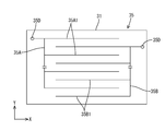
- the top view which shows typically the common electrode with which the display apparatus of FIG. 1 is provided.
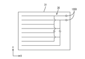
- the top view which shows typically the 2nd transparent electrode for switching liquid crystal panels with which the display apparatus of FIG. 1 is provided.
- the figure which shows the waveform of the pulse signal applied to a common electrode The figure which shows the waveform of the pulse signal applied to a common electrode.
- Sectional drawing which shows schematic structure of the display apparatus which concerns on Embodiment 2 of this invention.
- Sectional drawing which shows schematic structure of the display apparatus which concerns on Embodiment 3 of this invention.
- Sectional drawing which shows schematic structure of the display apparatus which concerns on Embodiment 4 of this invention.
- the top view which shows typically the common electrode which concerns on other embodiment.
- the top view which shows typically the 2nd transparent electrode for switching liquid crystal panels which concerns on other embodiment.
- the liquid crystal display device 10 (display device) is illustrated.
- the liquid crystal display device 10 is used as an information display element of various electronic devices (not shown) such as a portable information terminal, a mobile phone, a notebook computer, and a portable game machine.
- a part of each drawing shows an X axis, a Y axis, and a Z axis.
- the long side direction of the liquid crystal display device 10 is an X axis direction
- the short side direction is a Y axis direction.
- the vertical direction in FIG. 1 is the Z-axis direction (front and back direction, direction perpendicular to the screen), and the upper side in the figure is the front side and the lower side in the figure is the back side.
- the liquid crystal display device 10 has a rectangular shape (or square shape) in plan view as a whole, and as shown in FIG. 1, a backlight device 11, a liquid crystal display panel 20 (display panel), a switching liquid crystal panel 30 (parallax barrier), The touch panel 50 is mainly configured.
- the liquid crystal display panel 20, the switching liquid crystal panel 30, and the touch panel 50 are laminated in this order from the side close to the backlight device 11. That is, the touch panel 50 and the switching liquid crystal panel 30 are disposed on the display surface side of the liquid crystal display panel 20.
- the liquid crystal display panel 20, the switching liquid crystal panel 30, and the touch panel 50 are electrically connected to a control circuit board (not shown) via a flexible board (not shown), for example.
- the backlight device 11 includes a light source (for example, a cold cathode tube or an LED (not shown)) housed in a substantially box-shaped chassis that opens toward the front side (the liquid crystal display panel 20 side). It has a function of emitting light to the display panel 20 side.
- the backlight device 11 includes an optical member (not shown) arranged to cover the opening of the chassis. This optical member has a function of converting light emitted from a light source into a planar shape.
- the liquid crystal display panel 20 includes a pair of transparent (translucent) glass substrates 21 and 22 and liquid crystal molecules that are interposed between both the substrates 21 and 22 and whose optical characteristics change as an electric field is applied.
- a liquid crystal layer (not shown). Both substrates 21 and 22 are bonded together with a sealing agent (not shown) while maintaining a gap corresponding to the thickness of the liquid crystal layer.
- the front side (upper side in FIG. 1) is the CF substrate 21, and the back side (back side) is the TFT substrate 22 (element substrate).
- the TFT substrate 22 On the inner surface side (the liquid crystal layer side, the surface facing the CF substrate 21) of the TFT substrate 22, a large number of TFTs (Thin Film Transistors) and pixel electrodes are provided side by side (not shown).
- the TFT is a switching element for driving the liquid crystal for each pixel.
- a gate wiring and a source wiring having a lattice shape are disposed so as to surround them.
- the gate wiring and the source wiring are connected to the gate electrode and the source electrode of the TFT, respectively, and the pixel electrode is connected to the drain electrode of the TFT.
- This pixel electrode is made of a transparent electrode such as ITO (Indium Tin Oxide) or IZO (Indium Zinc Oxide).
- the CF substrate 21 is provided with a color filter in which colored portions such as R (red), G (green), and B (blue) are arranged in an array corresponding to each pixel.
- a light shielding layer black matrix
- a counter electrode facing the pixel electrode on the TFT substrate 22 side is provided on the surface of the color filter and the light shielding layer. As shown in FIG. 5, the counter electrode is electrically connected to the TFT substrate by, for example, a conductive member (for example, a conductive carbon paste).
- alignment films for aligning liquid crystal molecules contained in the liquid crystal layer are formed on the inner surfaces of both the substrates 21 and 22, respectively. Note that polarizing plates (not shown) are disposed on the outer surface sides of both the substrates 21 and 22, respectively.
- the switching liquid crystal panel 30 and the touch panel 50 are integrally arranged on the front side (upper side in FIG. 1) of the liquid crystal display panel 20 as described above.
- the switching liquid crystal panel 30 is arranged adjacent to the liquid crystal display panel 20 and can switch between two-dimensional display and three-dimensional display.
- the switching liquid crystal panel 30 includes transparent (translucent) glass substrates 31 and 32, a liquid crystal layer (not shown) interposed between the substrates 31 and 32, and polarized light disposed outside the liquid crystal layer. It has a board.
- the substrate 32 far from the liquid crystal display panel 20 is also a substrate constituting the touch panel 50, that is, a substrate commonly used for the switching liquid crystal panel 30 and the touch panel 50.
- the switching liquid crystal panel 30 includes a switching liquid crystal panel transparent electrode 33 for applying a voltage to a liquid crystal layer interposed between the substrates 31 and 32.
- the switching liquid crystal panel transparent electrode 33 includes two types of switching liquid crystal panel transparent electrodes 34 and 35 having different extending directions.
- the first switching liquid crystal panel transparent electrode 34 disposed on the touch panel 50 side of the switching liquid crystal panel transparent electrodes 34 and 35 is in the Y-axis direction (one side direction of the liquid crystal display device 10) as shown in FIG. It has a shape extending along.
- the first transparent electrode 34 for a switching liquid crystal panel is formed by arranging a plurality of comb-shaped electrodes 34A and 34B in the X-axis direction.
- an extending portion 34B1 (shape extending in the Y-axis direction) of the other electrode 34B is arranged between the extending portion 34A1 (shape extending in the Y-axis direction) of one electrode 34A. Is formed.
- the 1st transparent electrode 34 for switching liquid crystal panels is also what comprises a part of transparent electrode of the touch panel 50 mentioned later. That is, the first transparent electrode 34 for a switching liquid crystal panel is an electrode that is used in common for the switching liquid crystal panel 30 and the touch panel 50, and may be referred to as a common electrode 34 in the following description.
- the second switching liquid crystal panel transparent electrode 35 disposed on the liquid crystal display panel 20 side has a shape extending along the X-axis direction as shown in FIG.
- the switching liquid crystal panel transparent electrode 35 includes a plurality of comb-shaped electrodes 35A and 35B arranged in the X-axis direction.
- an extending portion 35B1 (shape extending in the X-axis direction) of the other electrode 35B is disposed between the extending portions 35A1 (shape extending in the X-axis direction) of one electrode 35A. Is formed.
- FIG. 3 only a part of the pair of electrodes 35A and 35B is shown.
- a voltage is applied to one of the pair of electrodes 34A and 34B constituting the first transparent liquid crystal panel electrode 34A, for example, the electrode 34A (the electrode 34B and the second transparent liquid crystal panel electrodes 35A and 35B are grounded).
- the switching liquid crystal panel 30 is configured to transmit light (light from the backlight device 11 via the liquid crystal display panel 20) only at a location corresponding to the extending portion 34A1 of the electrode 34A.
- the display of a specific pixel group in the liquid crystal display panel 20 can be visually recognized by the right eye, and the display of other pixel groups by the left eye, that is, the switching liquid crystal panel 30 can function as a parallax barrier. 3D display is possible.
- the switching liquid crystal panel 30 is configured to transmit light (light from the backlight device 11 via the liquid crystal display panel 20) only at a location (light transmission portion) corresponding to the extending portion 35A1 of the electrode 35A. ing. Accordingly, it is possible to visually recognize the display of a specific pixel group in the liquid crystal display panel 20 and the display of the other pixel group to the left eye, that is, the switching liquid crystal panel 30 can function as a parallax barrier. Three-dimensional display is possible.
- a parallax barrier in the long side direction and the short side direction of the liquid crystal display device 10 is formed. It is possible to perform three-dimensional display in each of two states of screen vertical installation and screen horizontal installation. Specifically, when a voltage is applied to the electrodes 34A, 35A, and 35B, three-dimensional display is possible with the Y-axis direction set to the vertical direction (relative to the user of the liquid crystal display device 10). , 34A, 34B, three-dimensional display is possible with the X-axis direction being the vertical orientation.
- the right-eye pixel and the left-eye pixel can be displayed on the liquid crystal display panel 20, respectively, and the right eye for the right eye of the user of the liquid crystal display device 10 through the light transmission portion formed on the switching liquid crystal panel 30.
- the pixel is configured such that the left eye pixel can be observed with the left eye.
- a voltage to both the first switching liquid crystal panel transparent electrode 34 and the switching liquid crystal panel transparent electrode 35, almost the entire surface of the switching liquid crystal panel 30 becomes a light transmitting portion, and two-dimensional display can be performed. Is possible.
- a normally black mode in which light is not transmitted when no voltage is applied is used as a switching liquid crystal mode.
- a normally white mode in which light is transmitted when no voltage is applied is used. Also good.
- the touch panel 50 is configured by forming the touch panel transparent electrodes 51 on both the front and back surfaces of the common substrate 32 described above.
- the touch panel transparent electrode 51 includes a common electrode 34 (first touch panel transparent electrode) extending along the Y-axis direction and an X-axis direction (direction intersecting the first touch panel transparent electrode).
- a second transparent electrode 52 for a touch panel see also FIG. 10.
- the second touch panel transparent electrode 52 is formed on the front side of the common substrate 32, and the common electrode 34 is formed on the back side of the common substrate 32.
- the second transparent electrode 52 for the touch panel is arranged on the common substrate 32 at a position opposite to the liquid crystal display panel 20 with respect to the common electrode 32.
- the touch panel 50 is input of data (for example, coordinate data on the touch panel 50) from a change in capacitance between the common electrode 34 and the second touch panel transparent electrode 52 generated by pointing the surface with a finger or the like. It is the composition which performs.
- the touch panel 50 in this embodiment is of a mutual capacitance detection method (Mutualaccapacitance Sensing), and is, for example, a first touch panel transparent electrode 34 (for example, the common electrodes 34A and 34B are regarded as one set).
- a pulse voltage is sequentially applied, a change in capacitance is detected by measuring the charge induced in the other electrode (second touch panel transparent electrode 52).
- the touch panel 50 and the switching liquid crystal panel 30 share the common substrate 32. Further, paying attention to the point that both the touch panel 50 and the switching liquid crystal panel 30 require a transparent electrode extending in the Y-axis direction, the transparent electrode extending in the Y-axis direction in both panels 30 and 50 is the same electrode (common electrode 34). It was set as the structure shared as.
- the pitch between adjacent extending portions 34A1 (that is, the minimum pitch of the light shielding barrier that can be formed in the switching liquid crystal panel 30) is set to 200 ⁇ m.
- 25 extension parts 34A1 are used as one set. That is, the resolution of the touch panel 50 in the X-axis direction is set to 5 mm. Note that the number of one set of the extending portions 34A1 can be changed as appropriate, and the pitch of each extending portion 34A1 can also be changed as appropriate.
- FIG. 4A and 4B are diagrams showing waveforms of a pulse signal for driving the touch panel 50 and a pulse signal for driving the switching liquid crystal panel 30 applied to the common electrode 34.
- FIG. 4A and 4B the horizontal axis represents time, and the vertical axis represents voltage.
- 4A shows the voltage applied to the electrode 34A
- FIG. 4B shows the voltage applied to the electrode 34B.
- the frequency (for example, several tens to several hundreds KHz) of the pulse signal for driving the touch panel 50 (indicated by symbol VSW) is the same as that of the pulse signal for driving the switching liquid crystal panel 30 (indicated by symbol VTP). It is set sufficiently higher than the frequency (for example, 60 Hz). As a result, it is possible to suppress a situation in which the driving voltages of the touch panel 50 and the switching liquid crystal panel 30 affect the driving of each other while the common electrode 34 is used as a common electrode.
- the voltage (for example, 5V) of the pulse signal VTP for driving the switching liquid crystal panel 30 is set to be higher than the voltage (for example, 3V) of the pulse signal VSW for driving the touch panel 50.
- the situation that affects the driving of the switching liquid crystal panel 30 can be suppressed.
- the liquid crystal display device 10 of this embodiment includes the liquid crystal display panel 20, the touch panel 50 disposed on the display surface side of the liquid crystal display panel 20, and the switching liquid crystal panel 30 that enables three-dimensional display.
- the touch panel 50 and the switching liquid crystal panel 30 are formed as an integral part by sharing a single common substrate 32.
- the common substrate 32 includes the touch panel transparent electrode 51 and the switching liquid crystal panel 30.
- a transparent electrode (common electrode 34) for switching liquid crystal panel for applying a voltage to the liquid crystal is formed.
- the touch panel 50 and the switching liquid crystal panel 30 are configured as an integral part, thereby achieving a reduction in thickness and weight.
- the touch panel transparent electrode 51 includes a first touch panel transparent electrode extending along the Y-axis direction and a second touch panel transparent electrode 52 extending along the X-axis direction, and is transparent for a switching liquid crystal panel.
- the electrode 33 includes a first switching liquid crystal panel transparent electrode extending in the same direction as the first touch panel transparent electrode and a second switching liquid crystal panel extending in the same direction as the second touch panel transparent electrode 52.
- the first transparent electrode for the touch panel and the transparent electrode for the first switching liquid crystal panel are made of the same electrode formed on the common substrate 32 on the liquid crystal display panel 20 side.
- the electrode 34 is configured.
- the first touch panel transparent electrode and the first switching liquid crystal panel transparent electrode are configured by the same common electrode 34, whereby the liquid crystal display device 10 is reduced in thickness and weight.
- Embodiment 2 of the present invention will be described with reference to FIG.
- the location where the second touch panel transparent electrode 52 is formed is different from that of the first embodiment.
- the second touch panel transparent electrode 52 is formed on the liquid crystal display panel 20 side of the common substrate 32, and specifically, is disposed between the common electrode 34 and the common substrate 32. Yes.
- An insulating layer 101 is formed between the common electrode 34 and the second touch panel transparent electrode 52.
- the touch panel 50 and the switching liquid crystal panel 30 can be configured as an integral part, and the liquid crystal display device 110 can be reduced in thickness and weight.
- Embodiment 3 of the present invention will be described with reference to FIG.
- the common electrode 34 is not provided, and the first touch panel transparent electrode 252 and the first switching liquid crystal panel transparent electrode 235 are separate members.
- the touch panel transparent electrode 51 is formed on the common substrate 32 on the side opposite to the liquid crystal display panel 20 (front side), and the switching liquid crystal panel transparent electrode 33 is formed on the common substrate 32 on the liquid crystal display panel 20 side. ing.
- the touch panel 50 and the switching liquid crystal panel 30 can be formed as an integral part by sharing the single common substrate 32, and the liquid crystal display device 210 can be made thinner and lighter. Can do.
- Embodiment 4 of the present invention will be described with reference to FIG.
- the switching liquid crystal panel 30, the liquid crystal display panel 20, and the touch panel 50 are stacked in this order from the side close to the backlight device 11.
- the touch panel 50 and the liquid crystal display panel 20 are formed as an integral part by sharing a single common substrate (CF substrate 21).
- the display device 310 can be reduced in thickness and weight.
- the touch panel 50 is exemplified by the mutual capacitance detection method, but the position detection method of the touch panel 50 is not limited to this.
- a position detection method of the touch panel 50 a method of directly measuring the capacitance of the sensor electrode of the touch panel 50 (self-capacitance detection method) may be used.
- the shape of the transparent electrode for the touch panel of the touch panel 50 is not limited to the shape as in the above embodiment (the shape in which the transparent electrodes extending in the X axis and the Y axis are overlapped in a lattice shape).
- the common electrode 34 In the third embodiment and the like that do not include the transparent electrode the transparent electrode may have a rhombus pattern (so-called diamond pattern).
- the drawing direction and the drawing position of the terminal portion (34D, 35D) to which the power supply is connected in the common electrode 34 and the transparent electrode 35 for the switching liquid crystal panel are not limited to those exemplified in the above embodiment, but can be changed as appropriate. Is possible.
- the electrodes 34 and 35 may be formed in such a manner that the lead-out positions of both terminal portions 134D (or 135D) are moved to one side.
- the transparent electrode extending in the X-axis direction is the common electrode 34.
- the present invention is not limited to this.
- a transparent electrode extending in the Y-axis direction may be used as a common electrode.
- the TFT is used as the switching element of the liquid crystal display device.
- the present invention can also be applied to a liquid crystal display device using a switching element other than TFT (for example, a thin film diode (TFD)), and color display.
- a switching element other than TFT for example, a thin film diode (TFD)
- color display for example, a liquid crystal display device.
- the present invention can be applied to a liquid crystal display device that displays black and white.
Abstract
Description
上記特許文献1の表示装置は、タッチパネルを備えるとともに、液晶パネルなどの表示パネルと、スイッチング液晶(視差バリア)を備えている。表示パネルには、右目用画素と左目用画素がそれぞれ表示され、スイッチング液晶に形成されたスリットを介して、観察者の右目で右目用画素を、左目で左目用画素を観察可能とする構成となっている。これにより、観察者は、両眼視差効果による立体映像を観察することができる。
上記課題を解決するために、本発明の表示装置は、表示パネルと、前記表示パネルの表示面側に配されたタッチパネルと、3次元表示を可能とする視差バリアと、を備え、前記表示パネル、前記タッチパネル、前記視差バリアのうち、少なくとも2つは一体部品として構成されていることに特徴を有する。
本発明によれば、タッチパネル及び立体映像を表示する機能を備えつつも、薄型化及び軽量化を実現可能な表示装置を提供することが可能となる。
本発明の実施形態1を図1ないし図4によって説明する。本実施形態では、液晶表示装置10(表示装置)について例示する。液晶表示装置10は、例えば、携帯型情報端末、携帯電話、ノートパソコン、携帯型ゲーム機などの各種電子機器(図示せず)の情報表示素子として用いられる。なお、各図面の一部にはX軸、Y軸及びZ軸を示しており、液晶表示装置10の長辺方向をX軸方向、短辺方向をY軸方向としている。また、図1における上下方向をZ軸方向(表裏方向、画面に垂直な方向)としており、同図上側を表側とするとともに同図下側を裏側とする。
次に、本発明の実施形態2を図5によって説明する。本実施形態の液晶表示装置110においては、第2のタッチパネル用透明電極52の形成箇所が上記実施形態1とは異なる。本実施形態においては、第2のタッチパネル用透明電極52が、共通基板32の液晶表示パネル20側に形成されており、具体的には、共通電極34と共通基板32との間に配されている。なお、共通電極34と第2のタッチパネル用透明電極52との間には、絶縁層101が形成されている。
次に、本発明の実施形態3を図6によって説明する。本実施形態の液晶表示装置210においては、共通電極34を備えず、第1のタッチパネル用透明電極252と、第1のスイッチング液晶パネル用透明電極235をそれぞれ別部材としている。また、タッチパネル用透明電極51は共通基板32において、液晶表示パネル20とは反対側(表側)に形成され、スイッチング液晶パネル用透明電極33は、共通基板32において、液晶表示パネル20側に形成されている。
次に、本発明の実施形態4を図7によって説明する。本実施形態の液晶表示装置310においては、バックライト装置11に近い側から、スイッチング液晶パネル30、液晶表示パネル20、タッチパネル50の順に積層されている。本実施形態においては、タッチパネル50及び液晶表示パネル20を、一枚の共通基板(CF基板21)を共有することで、一体部品として形成する構成となっており、このような構成としても、液晶表示装置310の薄型化及び軽量化を図ることができる。
本発明は上記記述及び図面によって説明した実施形態に限定されるものではなく、例えば次のような実施形態も本発明の技術的範囲に含まれる。
Claims (6)
- 表示パネルと、
前記表示パネルの表示面側に配されたタッチパネルと、
3次元表示を可能とする視差バリアと、を備え、
前記表示パネル、前記タッチパネル、前記視差バリアのうち、少なくとも2つは一体部品として構成されていることを特徴とする表示装置。 - 表示パネルと、
前記表示パネルの表示面側に配され、2次元表示と3次元表示とを切り替え可能なスイッチング液晶パネルと、
前記表示パネルの表示面側に配されたタッチパネルと、を備え、
前記タッチパネル及び前記スイッチング液晶パネルは、一枚の共通基板を共有することで一体部品として形成され、
前記共通基板には、タッチパネル用透明電極と、前記スイッチング液晶パネルの液晶に電圧を印加するためのスイッチング液晶パネル用透明電極とが形成されていることを特徴とする表示装置。 - 前記タッチパネル用透明電極は、
一方向に延びる第1のタッチパネル用透明電極と、
前記第1のタッチパネル用透明電極と交差する方向に延びる第2のタッチパネル用透明電極と、を備え、
前記スイッチング液晶パネル用透明電極は、
前記第1のタッチパネル用透明電極と同一方向に延びる第1のスイッチング液晶パネル用透明電極と、
前記第2のタッチパネル用透明電極と同一方向に延びる第2のスイッチング液晶パネル用透明電極と、を備えており、
前記第1のタッチパネル用透明電極及び前記第1のスイッチング液晶パネル用透明電極は、前記共通基板において前記表示パネル側に形成された同一の電極よりなる共通電極にて構成されていることを特徴とする請求項2に記載の表示装置。 - 前記第2のタッチパネル用透明電極は、前記共通基板において、前記共通電極よりも、前記表示パネルとは反対側となる位置に配されていることを特徴とする請求項3に記載の表示装置。
- 前記タッチパネル用透明電極は、前記共通基板において、前記表示パネルとは反対側に形成され、
前記スイッチング液晶パネル用透明電極は、前記共通基板において、前記表示パネル側に形成されていることを特徴とする請求項2に記載の表示装置。 - 前記表示パネルが液晶を用いた液晶表示パネルであることを特徴とする請求項1ないし請求項5のいずれか一項に記載の表示装置。
Priority Applications (4)
| Application Number | Priority Date | Filing Date | Title |
|---|---|---|---|
| US13/583,082 US8884922B2 (en) | 2010-04-01 | 2011-02-16 | Display device including touch panel and parallax barrier sharing single board |
| CN201180016848.8A CN102822778B (zh) | 2010-04-01 | 2011-02-16 | 显示装置 |
| JP2012509341A JP5383903B2 (ja) | 2010-04-01 | 2011-02-16 | 表示装置 |
| EP11765275.0A EP2533136B1 (en) | 2010-04-01 | 2011-02-16 | Display device |
Applications Claiming Priority (2)
| Application Number | Priority Date | Filing Date | Title |
|---|---|---|---|
| JP2010085530 | 2010-04-01 | ||
| JP2010-085530 | 2010-04-01 |
Publications (1)
| Publication Number | Publication Date |
|---|---|
| WO2011125373A1 true WO2011125373A1 (ja) | 2011-10-13 |
Family
ID=44762339
Family Applications (1)
| Application Number | Title | Priority Date | Filing Date |
|---|---|---|---|
| PCT/JP2011/053213 WO2011125373A1 (ja) | 2010-04-01 | 2011-02-16 | 表示装置 |
Country Status (5)
| Country | Link |
|---|---|
| US (1) | US8884922B2 (ja) |
| EP (1) | EP2533136B1 (ja) |
| JP (1) | JP5383903B2 (ja) |
| CN (1) | CN102822778B (ja) |
| WO (1) | WO2011125373A1 (ja) |
Cited By (16)
| Publication number | Priority date | Publication date | Assignee | Title |
|---|---|---|---|---|
| CN102707514A (zh) * | 2012-05-03 | 2012-10-03 | 北京京东方光电科技有限公司 | 一种3d触控液晶透镜光栅、显示装置及其制造方法 |
| CN102914895A (zh) * | 2012-09-21 | 2013-02-06 | 北京京东方光电科技有限公司 | 裸眼3d显示面板及其驱动方法 |
| CN103116230A (zh) * | 2011-11-17 | 2013-05-22 | 上海晨兴希姆通电子科技有限公司 | 3d触屏 |
| CN103164063A (zh) * | 2011-12-15 | 2013-06-19 | 宏碁股份有限公司 | 触控面板模块及触控立体显示装置 |
| CN103163677A (zh) * | 2011-12-15 | 2013-06-19 | 乐金显示有限公司 | 具有触摸和三维显示功能的液晶显示装置及其制造方法 |
| CN103293778A (zh) * | 2012-03-31 | 2013-09-11 | 上海天马微电子有限公司 | 一种触摸液晶光栅装置和3d/2d平板显示装置 |
| CN103293726A (zh) * | 2012-06-29 | 2013-09-11 | 上海天马微电子有限公司 | 液晶盒、3d触控显示装置及其控制方法 |
| US20130286304A1 (en) * | 2012-04-25 | 2013-10-31 | Au Optronics Corporation | Stereo display |
| US20140009819A1 (en) * | 2012-07-06 | 2014-01-09 | Hannstar Display Corp. | Stereoscopic image control module and stereoscopic display device |
| US20140015775A1 (en) * | 2012-07-16 | 2014-01-16 | Hannstar Display Corp. | Touch module with liquid crystal lens and display apparatus having the same |
| CN103576328A (zh) * | 2012-08-06 | 2014-02-12 | 韩国电子通信研究院 | 具有2d/3d 模式转换的基于分段视差屏障的显示设备及方法 |
| CN104105999A (zh) * | 2012-02-15 | 2014-10-15 | 夏普株式会社 | 立体显示装置 |
| JP2014199594A (ja) * | 2013-03-29 | 2014-10-23 | 株式会社ジャパンディスプレイ | タッチ検出機能付き表示装置、電子機器及びタッチ検出デバイス |
| WO2016011713A1 (zh) * | 2014-07-24 | 2016-01-28 | 京东方科技集团股份有限公司 | 镜面显示装置控制方法、控制装置和控制系统 |
| JP2016224728A (ja) * | 2015-05-29 | 2016-12-28 | 株式会社ジャパンディスプレイ | センサ付き表示装置 |
| US9581823B2 (en) | 2013-06-25 | 2017-02-28 | Au Optronics Corporation | 2D/3D switchable display device and manufacturing method thereof |
Families Citing this family (12)
| Publication number | Priority date | Publication date | Assignee | Title |
|---|---|---|---|---|
| US20130088659A1 (en) * | 2010-06-02 | 2013-04-11 | Sharp Kabushiki Kaisha | Liquid crystal display device |
| KR101188983B1 (ko) | 2010-09-30 | 2012-10-08 | 삼성디스플레이 주식회사 | 터치 스크린 패널 내장형 입체 영상 평판표시장치 |
| EP2690614B1 (en) * | 2011-04-22 | 2017-08-16 | Sharp Kabushiki Kaisha | Display device |
| CN103268176B (zh) * | 2012-12-11 | 2016-03-02 | 上海天马微电子有限公司 | 一种互感式电容触摸屏 |
| CN103116233B (zh) * | 2013-01-23 | 2016-01-06 | 北京京东方光电科技有限公司 | 一种触摸液晶光栅结构及3d触摸显示装置 |
| CN103091909B (zh) * | 2013-01-29 | 2015-10-14 | 北京京东方光电科技有限公司 | 一种触控3d显示模组及其制作方法和触控3d显示装置 |
| US9058780B2 (en) * | 2013-03-08 | 2015-06-16 | Innolux Corporation | 2D/3D switchable and touch sensitive display and method for driving the same |
| CN103149732A (zh) * | 2013-03-25 | 2013-06-12 | 京东方科技集团股份有限公司 | 一种显示面板及3d显示装置 |
| TWI493408B (zh) | 2013-08-01 | 2015-07-21 | Au Optronics Corp | 整合觸控結構的光學切換裝置與立體顯示裝置 |
| CN104123036B (zh) * | 2014-06-09 | 2017-02-01 | 京东方科技集团股份有限公司 | 光栅基板及其制作方法、显示装置 |
| KR102347852B1 (ko) * | 2014-09-05 | 2022-01-06 | 삼성전자주식회사 | 터치 스크린 패널, 전자 노트 및 휴대용 단말기 |
| DE102014114686A1 (de) * | 2014-10-09 | 2016-04-14 | Carl Zeiss Meditec Ag | Anzeigegerät mit dreidimensionaler Bildausgabe und berührungsempfindlichem Display |
Citations (2)
| Publication number | Priority date | Publication date | Assignee | Title |
|---|---|---|---|---|
| JP2004272354A (ja) | 2003-03-05 | 2004-09-30 | Sanyo Electric Co Ltd | 立体表示型操作パネル |
| WO2009069358A1 (ja) * | 2007-11-29 | 2009-06-04 | Sharp Kabushiki Kaisha | 表示装置 |
Family Cites Families (11)
| Publication number | Priority date | Publication date | Assignee | Title |
|---|---|---|---|---|
| DE19925985A1 (de) * | 1999-06-08 | 2000-12-14 | Bosch Gmbh Robert | Flüssigkristallanzeige mit umschaltbarem Blickwinkel |
| GB2426352A (en) * | 2005-05-21 | 2006-11-22 | Sharp Kk | A switchable multi-view display |
| KR101201848B1 (ko) * | 2006-02-20 | 2012-11-15 | 삼성디스플레이 주식회사 | 입체영상 변환패널 및 이를 갖는 입체영상 표시장치 |
| EP2027526A2 (en) * | 2006-06-09 | 2009-02-25 | Apple, Inc. | Touch screen liquid crystal display |
| US8243027B2 (en) * | 2006-06-09 | 2012-08-14 | Apple Inc. | Touch screen liquid crystal display |
| KR100824539B1 (ko) * | 2007-01-02 | 2008-04-24 | 삼성에스디아이 주식회사 | 터치패널 겸용 입체 영상 디스플레이 장치 |
| KR101086422B1 (ko) * | 2007-01-05 | 2011-11-25 | 삼성전자주식회사 | 고효율 2차원/3차원 겸용 영상 표시장치 |
| JP5246746B2 (ja) * | 2008-01-21 | 2013-07-24 | 株式会社ジャパンディスプレイウェスト | 電気光学装置、電気光学装置の製造方法及び電子機器 |
| WO2009105544A2 (en) * | 2008-02-19 | 2009-08-27 | The Board Of Trustees Of The University Of Illinois | Large format high resolution interactive display |
| JP5481040B2 (ja) * | 2008-04-11 | 2014-04-23 | 株式会社ジャパンディスプレイ | 表示装置とその駆動方法 |
| US8643624B2 (en) * | 2009-03-18 | 2014-02-04 | Synaptics Incorporated | Capacitive sensing using a segmented common voltage electrode of a display |
-
2011
- 2011-02-16 WO PCT/JP2011/053213 patent/WO2011125373A1/ja active Application Filing
- 2011-02-16 CN CN201180016848.8A patent/CN102822778B/zh not_active Expired - Fee Related
- 2011-02-16 US US13/583,082 patent/US8884922B2/en not_active Expired - Fee Related
- 2011-02-16 EP EP11765275.0A patent/EP2533136B1/en not_active Not-in-force
- 2011-02-16 JP JP2012509341A patent/JP5383903B2/ja active Active
Patent Citations (2)
| Publication number | Priority date | Publication date | Assignee | Title |
|---|---|---|---|---|
| JP2004272354A (ja) | 2003-03-05 | 2004-09-30 | Sanyo Electric Co Ltd | 立体表示型操作パネル |
| WO2009069358A1 (ja) * | 2007-11-29 | 2009-06-04 | Sharp Kabushiki Kaisha | 表示装置 |
Cited By (29)
| Publication number | Priority date | Publication date | Assignee | Title |
|---|---|---|---|---|
| CN103116230A (zh) * | 2011-11-17 | 2013-05-22 | 上海晨兴希姆通电子科技有限公司 | 3d触屏 |
| US10175801B2 (en) | 2011-12-15 | 2019-01-08 | Lg Display Co., Ltd. | Liquid crystal display device having touch and three-dimensional display functions and method for manufacturing the same |
| CN103164063A (zh) * | 2011-12-15 | 2013-06-19 | 宏碁股份有限公司 | 触控面板模块及触控立体显示装置 |
| CN103163677A (zh) * | 2011-12-15 | 2013-06-19 | 乐金显示有限公司 | 具有触摸和三维显示功能的液晶显示装置及其制造方法 |
| US9766736B2 (en) | 2011-12-15 | 2017-09-19 | Lg Display Co., Ltd. | Liquid crystal display device having touch and three-dimensional display functions and method for manufacturing the same |
| US9141223B2 (en) | 2011-12-15 | 2015-09-22 | Lg Display Co., Ltd. | Liquid crystal display device having touch and three-dimensional display functions and method for manufacturing the same |
| KR101535823B1 (ko) * | 2011-12-15 | 2015-07-13 | 엘지디스플레이 주식회사 | 터치 및 입체 영상 표시 기능을 갖는 액정표시장치 및 그의 제조 방법 |
| CN104105999A (zh) * | 2012-02-15 | 2014-10-15 | 夏普株式会社 | 立体显示装置 |
| EP2806304A4 (en) * | 2012-02-15 | 2015-03-04 | Sharp Kk | THREE-DIMENSIONAL DISPLAY DEVICE |
| CN103293778A (zh) * | 2012-03-31 | 2013-09-11 | 上海天马微电子有限公司 | 一种触摸液晶光栅装置和3d/2d平板显示装置 |
| US20130286304A1 (en) * | 2012-04-25 | 2013-10-31 | Au Optronics Corporation | Stereo display |
| CN102707514A (zh) * | 2012-05-03 | 2012-10-03 | 北京京东方光电科技有限公司 | 一种3d触控液晶透镜光栅、显示装置及其制造方法 |
| WO2013163882A1 (zh) * | 2012-05-03 | 2013-11-07 | 北京京东方光电科技有限公司 | 3d触控液晶透镜光栅、其制造方法以及3d触控显示装置 |
| KR101530794B1 (ko) * | 2012-05-03 | 2015-06-22 | 베이징 비오이 옵토일렉트로닉스 테크놀로지 컴퍼니 리미티드 | 3d 터치 제어 액정 렌즈 격자, 그 제조 방법, 및 3d 터치 제어 디스플레이 장치 |
| JP2015521299A (ja) * | 2012-05-03 | 2015-07-27 | 北京京東方光電科技有限公司 | 3dタッチ液晶レンズ格子、その製造方法及び3dタッチ表示装置 |
| EP2848990A4 (en) * | 2012-05-03 | 2015-12-30 | Beijing Boe Optoelectronics | 3D LIQUID CRYSTAL LENS GRILLE, METHOD OF MANUFACTURING THEREOF AND 3D TOUCH DISPLAY DEVICE |
| WO2014000366A1 (zh) * | 2012-06-29 | 2014-01-03 | 上海天马微电子有限公司 | 液晶盒、3d显示装置及其控制方法 |
| CN103293726A (zh) * | 2012-06-29 | 2013-09-11 | 上海天马微电子有限公司 | 液晶盒、3d触控显示装置及其控制方法 |
| US20140009819A1 (en) * | 2012-07-06 | 2014-01-09 | Hannstar Display Corp. | Stereoscopic image control module and stereoscopic display device |
| US20140015775A1 (en) * | 2012-07-16 | 2014-01-16 | Hannstar Display Corp. | Touch module with liquid crystal lens and display apparatus having the same |
| CN103576328A (zh) * | 2012-08-06 | 2014-02-12 | 韩国电子通信研究院 | 具有2d/3d 模式转换的基于分段视差屏障的显示设备及方法 |
| CN102914895A (zh) * | 2012-09-21 | 2013-02-06 | 北京京东方光电科技有限公司 | 裸眼3d显示面板及其驱动方法 |
| JP2014199594A (ja) * | 2013-03-29 | 2014-10-23 | 株式会社ジャパンディスプレイ | タッチ検出機能付き表示装置、電子機器及びタッチ検出デバイス |
| US9581823B2 (en) | 2013-06-25 | 2017-02-28 | Au Optronics Corporation | 2D/3D switchable display device and manufacturing method thereof |
| WO2016011713A1 (zh) * | 2014-07-24 | 2016-01-28 | 京东方科技集团股份有限公司 | 镜面显示装置控制方法、控制装置和控制系统 |
| JP2016224728A (ja) * | 2015-05-29 | 2016-12-28 | 株式会社ジャパンディスプレイ | センサ付き表示装置 |
| US10152168B2 (en) | 2015-05-29 | 2018-12-11 | Japan Display Inc. | Sensor-equipped display device |
| US10739905B2 (en) | 2015-05-29 | 2020-08-11 | Japan Display Inc. | Sensor-equipped display device |
| US11373611B2 (en) | 2015-05-29 | 2022-06-28 | Japan Display Inc. | Sensor-equipped display device |
Also Published As
| Publication number | Publication date |
|---|---|
| CN102822778A (zh) | 2012-12-12 |
| EP2533136B1 (en) | 2018-10-31 |
| CN102822778B (zh) | 2015-07-22 |
| EP2533136A1 (en) | 2012-12-12 |
| US20120327005A1 (en) | 2012-12-27 |
| EP2533136A4 (en) | 2015-08-05 |
| JP5383903B2 (ja) | 2014-01-08 |
| JPWO2011125373A1 (ja) | 2013-07-08 |
| US8884922B2 (en) | 2014-11-11 |
Similar Documents
| Publication | Publication Date | Title |
|---|---|---|
| JP5383903B2 (ja) | 表示装置 | |
| US10459303B2 (en) | Display device with curved part | |
| US10261617B2 (en) | In-cell touch panel and display device | |
| US20130155059A1 (en) | Switchable touch stereoscopic image device | |
| JP5306059B2 (ja) | タッチパネル、表示パネル、タッチパネル用基板、表示パネル用基板および表示装置 | |
| WO2015107969A1 (ja) | 位置入力装置及び表示装置 | |
| JP5807035B2 (ja) | タッチ検出機能付き表示装置、電子機器及びタッチ検出デバイス | |
| KR20090080487A (ko) | 전기 광학 장치, 전기 광학 장치의 제조 방법 및 전자 기기 | |
| JP5923456B2 (ja) | 表示装置 | |
| WO2016039244A1 (ja) | 位置入力装置、及び位置入力機能付き表示装置 | |
| JP2019101095A (ja) | 液晶パネル | |
| JP5604359B2 (ja) | 表示パネル、表示装置および電子機器 | |
| JP5555142B2 (ja) | 表示装置 | |
| JP2012242817A (ja) | 表示装置 | |
| JP5659294B2 (ja) | 表示装置 | |
| WO2012121091A1 (ja) | タッチパネル制御回路、表示装置の駆動回路、および表示装置 | |
| JP2020042192A (ja) | 表示装置及びミラー装置 | |
| JP2014021865A (ja) | タッチパネル付液晶表示装置及びタッチパネル付液晶表示装置の製造方法 | |
| JP5778592B2 (ja) | 表示装置、タッチ検出装置および電子機器 | |
| US10795482B2 (en) | Touch panel and electronic device | |
| US20130114024A1 (en) | Display apparatus and electronic equipment | |
| JP6006380B2 (ja) | 表示装置、タッチ検出装置および電子機器 | |
| JP2014074734A (ja) | 液晶表示装置 | |
| JPWO2016136662A1 (ja) | タッチセンサ付き表示装置 | |
| WO2018212034A1 (ja) | 位置入力機能付き表示装置 |
Legal Events
| Date | Code | Title | Description |
|---|---|---|---|
| WWE | Wipo information: entry into national phase |
Ref document number: 201180016848.8 Country of ref document: CN |
|
| 121 | Ep: the epo has been informed by wipo that ep was designated in this application |
Ref document number: 11765275 Country of ref document: EP Kind code of ref document: A1 |
|
| WWE | Wipo information: entry into national phase |
Ref document number: 2011765275 Country of ref document: EP |
|
| WWE | Wipo information: entry into national phase |
Ref document number: 13583082 Country of ref document: US |
|
| WWE | Wipo information: entry into national phase |
Ref document number: 2012509341 Country of ref document: JP |
|
| NENP | Non-entry into the national phase |
Ref country code: DE |