WO2011122235A1 - 光沢ニッケルめっき材、光沢ニッケルめっき材を用いた電子部品、及び、光沢ニッケルめっき材の製造方法 - Google Patents
光沢ニッケルめっき材、光沢ニッケルめっき材を用いた電子部品、及び、光沢ニッケルめっき材の製造方法 Download PDFInfo
- Publication number
- WO2011122235A1 WO2011122235A1 PCT/JP2011/054954 JP2011054954W WO2011122235A1 WO 2011122235 A1 WO2011122235 A1 WO 2011122235A1 JP 2011054954 W JP2011054954 W JP 2011054954W WO 2011122235 A1 WO2011122235 A1 WO 2011122235A1
- Authority
- WO
- WIPO (PCT)
- Prior art keywords
- nickel plating
- plating material
- bright
- plating
- layer
- Prior art date
- Legal status (The legal status is an assumption and is not a legal conclusion. Google has not performed a legal analysis and makes no representation as to the accuracy of the status listed.)
- Ceased
Links
Images
Classifications
-
- C—CHEMISTRY; METALLURGY
- C25—ELECTROLYTIC OR ELECTROPHORETIC PROCESSES; APPARATUS THEREFOR
- C25D—PROCESSES FOR THE ELECTROLYTIC OR ELECTROPHORETIC PRODUCTION OF COATINGS; ELECTROFORMING; APPARATUS THEREFOR
- C25D5/00—Electroplating characterised by the process; Pretreatment or after-treatment of workpieces
- C25D5/34—Pretreatment of metallic surfaces to be electroplated
-
- C—CHEMISTRY; METALLURGY
- C25—ELECTROLYTIC OR ELECTROPHORETIC PROCESSES; APPARATUS THEREFOR
- C25D—PROCESSES FOR THE ELECTROLYTIC OR ELECTROPHORETIC PRODUCTION OF COATINGS; ELECTROFORMING; APPARATUS THEREFOR
- C25D3/00—Electroplating: Baths therefor
- C25D3/02—Electroplating: Baths therefor from solutions
- C25D3/12—Electroplating: Baths therefor from solutions of nickel or cobalt
-
- C—CHEMISTRY; METALLURGY
- C25—ELECTROLYTIC OR ELECTROPHORETIC PROCESSES; APPARATUS THEREFOR
- C25D—PROCESSES FOR THE ELECTROLYTIC OR ELECTROPHORETIC PRODUCTION OF COATINGS; ELECTROFORMING; APPARATUS THEREFOR
- C25D3/00—Electroplating: Baths therefor
- C25D3/02—Electroplating: Baths therefor from solutions
- C25D3/12—Electroplating: Baths therefor from solutions of nickel or cobalt
- C25D3/14—Electroplating: Baths therefor from solutions of nickel or cobalt from baths containing acetylenic or heterocyclic compounds
- C25D3/16—Acetylenic compounds
-
- C—CHEMISTRY; METALLURGY
- C25—ELECTROLYTIC OR ELECTROPHORETIC PROCESSES; APPARATUS THEREFOR
- C25D—PROCESSES FOR THE ELECTROLYTIC OR ELECTROPHORETIC PRODUCTION OF COATINGS; ELECTROFORMING; APPARATUS THEREFOR
- C25D3/00—Electroplating: Baths therefor
- C25D3/02—Electroplating: Baths therefor from solutions
- C25D3/12—Electroplating: Baths therefor from solutions of nickel or cobalt
- C25D3/14—Electroplating: Baths therefor from solutions of nickel or cobalt from baths containing acetylenic or heterocyclic compounds
- C25D3/18—Heterocyclic compounds
-
- C—CHEMISTRY; METALLURGY
- C25—ELECTROLYTIC OR ELECTROPHORETIC PROCESSES; APPARATUS THEREFOR
- C25D—PROCESSES FOR THE ELECTROLYTIC OR ELECTROPHORETIC PRODUCTION OF COATINGS; ELECTROFORMING; APPARATUS THEREFOR
- C25D5/00—Electroplating characterised by the process; Pretreatment or after-treatment of workpieces
- C25D5/34—Pretreatment of metallic surfaces to be electroplated
- C25D5/36—Pretreatment of metallic surfaces to be electroplated of iron or steel
Definitions
- the present invention relates to a bright nickel plating material, an electronic component using the bright nickel plating material, and a method for producing the bright nickel plating material.
- a problem in producing bright nickel plating is that the appearance of the plating is affected by the surface characteristics of the plating material. For example, when applying bright nickel plating to brass (Cu-30% Zn) strips, if the brass material is an annealed material, the appearance after plating will not show a good gloss, or a cloudy appearance, or gloss and cloudiness May be mixed. Similar problems have also been confirmed when bright nickel plating is applied to phosphor bronze (Cu-8% Sn-P) strips.
- Patent Document 1 discloses a method for producing a copper alloy having excellent plating properties. And according to this, it is described that silver plating or copper plating can be particularly favorably formed by thinning the work-affected layer on the surface of the copper alloy.
- this invention makes it a subject to provide the manufacturing method of the bright nickel plating material which has a favorable external appearance, the electronic component using the bright nickel plating material, and a bright nickel plating material.
- the present invention completed on the basis of the above knowledge, in one aspect, comprises a metal base material having a thickness of 0.2 ⁇ m or more of a work-affected layer on the surface, and a nickel plating layer formed on the surface of the metal base material.
- a bright nickel plating material provided.
- the thickness of the work-affected layer is 0.25 to 3.0 ⁇ m.
- the thickness of the work-affected layer is 0.3 to 2.0 ⁇ m.
- the crystal grain size of nickel constituting the nickel plating layer is 0.3 ⁇ m or less.
- the crystal grain size of nickel constituting the nickel plating layer is 0.01 to 0.3 ⁇ m.
- the metal substrate is formed of stainless steel, copper, or a copper alloy.
- the present invention is an electronic component using the bright nickel plating material according to the present invention.
- a method for producing a bright nickel-plated material comprising preparing a metal base material having a surface-affected layer having a thickness of 0.2 ⁇ m or more and forming a nickel plating layer on the surface. .
- the crystal grain size of nickel constituting the nickel plating layer is 0.01 to 0.3 ⁇ m or less.
- the present invention it is possible to provide a bright nickel plating material having a good appearance, an electronic component using the bright nickel plating material, and a method for producing the bright nickel plating material.
- Metal base material Although there is no restriction
- a material having a high electrical conductivity for example, IACS (International Anneal Copper Standard: a value when the conductivity of an international standard annealed copper is 100) is about 15 to 80%
- IACS International Anneal Copper Standard: a value when the conductivity of an international standard annealed copper is 100
- Cu—Sn—P for example, phosphor bronze
- Cu—Zn for example, brass, red
- Cu—Ni—Zn for example, white
- Cu—Fe—P for example Is mentioned.
- limiting in particular in the shape of a metal base material Forms, such as a board, a strip, and a press product, may be sufficient.
- a work-affected layer is present at a thickness of 0.2 ⁇ m or more on the surface of the metal substrate to which nickel plating is applied.
- the work-affected layer is a fine layer of crystal flow generated on the metal surface by rolling or buffing.
- the thickness of the work-affected layer is preferably 0.25 to 3.0 ⁇ m, more preferably 0.3 to 2.0 ⁇ m.
- nickel plating when manufacturing a bright nickel plating material, a plating film is formed on a metal substrate using plating containing a brightener, but the nickel plating has a glossy appearance depending on the state of the metal substrate surface as described above. It may not be.
- nickel plating has a characteristic that it is easily influenced by the underlying metal crystal. For example, if the crystal grains of the metal substrate are coarse, the crystal grains of the plating also increase, and as a result, the unevenness of the plating surface increases. For this reason, it becomes a cloudy appearance.
- the crystal grains of the metal substrate are fine, the plating structure becomes fine and the plating surface becomes smooth. For this reason, the plating has a glossy appearance.
- a nickel plating layer is formed on the processed surface of the above-described metal substrate.
- the nickel plating layer is made of nickel having a crystal grain size (0.3 ⁇ m or less) corresponding to the crystal grain size of the metal on the surface of the metal substrate. Since the nickel plating layer has such a fine crystal grain size, it has a good gloss.
- the crystal grain size of nickel constituting the nickel plating layer is preferably 0.01 to 0.3 ⁇ m.
- the nickel plating layer is made of nickel, and this contains a very small amount of an organic brightener component. This is because a slight amount of the brightener component is taken into the film during the plating process.
- electronic parts such as terminals and connectors according to the present invention are made of the above-described bright nickel plating material.
- a metal substrate formed of stainless steel, copper, copper alloy or the like is prepared.
- a work-affected layer is formed on the surface of the metal substrate by, for example, rolling, skin pass rolling, buffing, or brushing.
- the processing conditions such as the degree of rolling, the pressure during buffing and the time are adjusted so that the thickness of the work-affected layer is 0.2 ⁇ m or more.
- the processing-affected layer is observed by cross-sectional observation using FIB (Focused Ion Beam) to confirm the success or failure of the processing.
- the bright plating solution used for the bright plating bath contains a water-soluble nickel salt, a pH buffer, and a brightener.
- the water-soluble nickel salt include nickel sulfate and nickel chloride, and a total of 250 to 350 g / L is added.
- the pH buffering agent include boric acid and citric acid, and these are added in an amount of 35 to 45 g / L.
- the brightener include saccharin and 1-4 butynediol, and these are added in an amount of 0.1 to 2 g / L.
- the bright plating solution is an aqueous solution, preferably adjusted to pH 3 to 5, and more preferably adjusted to pH 3.8 to 4.2.
- the bright plating solution is preferably used at a bath temperature of 40 to 60 ° C., more preferably 45 to 50 ° C.
- a bath temperature of 40 to 60 ° C. more preferably 45 to 50 ° C.
- the above-described metal substrate with the processed surface is immersed in a bright plating bath for a predetermined time to obtain a bright nickel-plated substrate having a desired gloss.
- a work-affected layer having a crystal grain size of 1 ⁇ m or less, preferably about 0.01 to 0.2 ⁇ m is formed on the surface of the metal substrate, the metal crystal grains of the plating layer formed on the surface The diameter also becomes correspondingly fine. For this reason, the surface of the formed plating layer becomes smooth and good gloss can be obtained.
- Example 1 Examples 1 to 10.
- a brass plate having a thickness of 0.65 mm was prepared as a metal substrate.
- a work-affected layer having a thickness shown in Table 1 was formed by buffing. The thickness of this deteriorated layer is observed using FIB. Further, the crystal grain size of the metal constituting the work-affected layer of the metal substrate was observed by FIB.
- a bright plating bath containing a bright plating solution having the following composition was prepared.
- Example 2 Comparative Examples 1 to 5
- Example 1 to 5 Comparative Examples 1 to 5
- a plating bath similar to that of the example was prepared, and plating was performed without processing the surface of the brass plate or by performing minor processing such as light brush polishing.
- the plating current and bath temperature were also set in the same manner as in the examples.
Landscapes
- Chemical & Material Sciences (AREA)
- Engineering & Computer Science (AREA)
- Chemical Kinetics & Catalysis (AREA)
- Electrochemistry (AREA)
- Materials Engineering (AREA)
- Metallurgy (AREA)
- Organic Chemistry (AREA)
- Electroplating Methods And Accessories (AREA)
- Electroplating And Plating Baths Therefor (AREA)
- Mechanical Engineering (AREA)
Abstract
Description
本発明に用いることのできる金属基材の形態に特に制限はないが、例えば、ステンレス鋼、銅、又は、銅合金が挙げられる。このうち、ステンレス鋼としては、マルテンサイト系、フェライト系、オーステナイト系等を用いることができる。また、銅又は銅合金は、コネクタや端子等の電子部品に使われる母材として公知である任意の銅又は銅合金としてよいが、電気・電子機器の接続端子等に用いられることを考慮すれば、電気伝導率の高いもの(例えば、IACS(International Anneild Copper Standerd:国際標準軟銅の導電率を100とした時の値)が15~80%程度)を用いるのが好ましく、例えばCu-Sn-P系(例えばりん青銅)、Cu-Zn系(例えば黄銅、丹銅)、Cu-Ni-Zn系(例えば洋白)、Cu-Ni-Si系(コルソン合金)、Cu-Fe-P系合金などが挙げられる。また、金属基材の形状には特に制限はなく、板、条及びプレス品等の形態であってもよい。
一方、光沢ニッケルめっき材を製造する場合には、光沢剤を含有するめっきを用いて金属基材にめっき被膜を形成するが、上述のように金属基材表面の状態により、ニッケルめっきが光沢外観にならない場合がある。ニッケルめっきは下地の金属結晶の影響を受けやすいという特性を有するためである。例えば、金属基材の結晶粒が粗大であれば、めっきの結晶粒も大きくなり、結果としてめっき表面の凹凸が大きくなる。このため、曇った外観となる。一方、金属基材の結晶粒が微細であれば、めっき組織も微細となり、めっき表面は平滑になる。このため、めっきは光沢外観となる。
本発明に係る光沢ニッケルめっき材は、上述の金属基材の加工された表面に、ニッケルめっき層が形成されている。ニッケルめっき層は、金属基材の表面の金属の結晶粒径に対応する大きさの結晶粒径(0.3μm以下)を有するニッケルで構成されている。ニッケルめっき層は、このように結晶粒径が微細であるため、良好な光沢を有している。また、ニッケルめっき層を構成するニッケルの結晶粒径は、好ましくは0.01~0.3μmである。
また、本発明に係る端子、コネクタ等の電子部品は、上述の光沢ニッケルめっき材を材料として構成されている。
まず、ステンレス鋼、銅、又は、銅合金等で形成された金属基材を準備する。次に、例えば、圧延、スキンパス圧延、バフ研磨、ブラシ研磨によって金属基材の表面に加工変質層を形成する。加工変質層の厚さが0.2μm以上になるように加工の条件、例えば圧延加工度、バフ研磨時の圧力や時間を調整する。加工変質層の観察は、FIB(Focused Ion Beam)による断面観察で行い、加工の成否を確認する。
ここで、水溶性ニッケル塩としては、例えば硫酸ニッケル、塩化ニッケル等が挙げられ、これらは合計250~350g/L添加される。
pH緩衝剤としては、例えば、ホウ酸、クエン酸等が挙げられ、これらは35~45g/L添加される。
光沢剤としては、例えば、サッカリン、1-4ブチンジオールが挙げられ、これらは0.1~2g/L添加される。
また、光沢めっき液は、浴温40~60℃で使用するのが好ましく、45~50℃で使用するのがより好ましい。
光沢めっき液のpH及び浴温が上記範囲外の場合、めっき速度が遅かったり、外観不良を起し易い等の問題がある。
金属基材として、厚さ0.65mmの黄銅板を準備した。黄銅板の表面には、バフ研磨により表1に示す厚さの加工変質層を形成した。この変質層の厚さは、FIBを用いて観察したものである。
また、金属基材の加工変質層を構成する金属の結晶粒径をFIBにより観察した。
続いて、以下の組成の光沢めっき液を含有する光沢めっき浴を準備した。
・NiSO4・6H2O 250g/l
・NiCl2・6H2O 50g/l
・ホウ酸 40サッカリン 2g/l
・1,4-ブチンジオール 0.2g/l
次に、表面を加工した黄銅板を脱脂、酸洗した後、めっき浴に浸漬させ電流密度5A/dm2でめっき層を形成した。光沢めっき浴は、pH4.0で45℃とした。
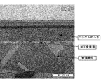
図1に、実施例3に係る黄銅基材、加工変質層及びニッケルめっき層の拡大断面図を示す。
比較例1~5として、まず、実施例と同様の銅箔を準備した。次に、実施例と同様のめっき浴を準備して、これに該黄銅板表面を加工しないで、あるいは軽くブラシ研磨する等の軽微な加工を行ってめっきした。めっき電流、及び浴温も実施例と同様に設定した。
ニッケルめっき層を構成するニッケルの結晶粒径をFIBでの断面像により観察した。
ニッケルめっき層の光沢について外観観察を行った。外観評価は、光沢度計(日本電色工業製反射濃度計ND-1)を用いて行い、測定値が1.8超であるときを○とし、1.6~1.8であるときを△とし、1.6未満であるときを×と評価した。
例1及び2の結果を表1に示す。

Claims (9)
- 表面の加工変質層の厚さが0.2μm以上である金属基材と、該金属基材の該表面に形成したニッケルめっき層とを備えた光沢ニッケルめっき材。
- 前記加工変質層の厚さが0.25~3.0μmである請求項1に記載の光沢ニッケルめっき材。
- 前記加工変質層の厚さが0.3~2.0μmである請求項2に記載の光沢ニッケルめっき材。
- 前記ニッケルめっき層を構成するニッケルの結晶粒径が0.3μm以下である請求項1~3のいずれかに記載の光沢ニッケルめっき材。
- 前記ニッケルめっき層を構成するニッケルの結晶粒径が0.01~0.3μmである請求項4に記載の光沢ニッケルめっき材。
- 金属基材が、ステンレス、銅、又は、銅合金で形成されている請求項1~5のいずれかに記載の光沢ニッケルめっき材。
- 請求項1~6のいずれかに記載の光沢ニッケルめっき材を用いた電子部品。
- 表面の加工変質層の厚さが0.2μm以上である金属基材を準備し、該表面にニッケルめっき層を形成する光沢ニッケルめっき材の製造方法。
- 前記ニッケルめっき層を構成するニッケルの結晶粒径が0.01~0.3μmである請求項8に記載の光沢ニッケルめっき材の製造方法。
Priority Applications (4)
| Application Number | Priority Date | Filing Date | Title |
|---|---|---|---|
| CN201180016871.7A CN102812165B (zh) | 2010-03-31 | 2011-03-03 | 光泽镀镍材料、使用光泽镀镍材料的电子零件及光泽镀镍材料的制备方法 |
| KR1020127028203A KR20130027492A (ko) | 2010-03-31 | 2011-03-03 | 광택 니켈 도금재, 광택 니켈 도금재를 사용한 전자 부품 및 광택 니켈 도금재의 제조 방법 |
| KR1020157026833A KR20150115962A (ko) | 2010-03-31 | 2011-03-03 | 광택 니켈 도금재, 광택 니켈 도금재를 사용한 전자 부품 및 광택 니켈 도금재의 제조 방법 |
| KR1020147027348A KR20140121899A (ko) | 2010-03-31 | 2011-03-03 | 광택 니켈 도금재, 광택 니켈 도금재를 사용한 전자 부품 및 광택 니켈 도금재의 제조 방법 |
Applications Claiming Priority (2)
| Application Number | Priority Date | Filing Date | Title |
|---|---|---|---|
| JP2010-083223 | 2010-03-31 | ||
| JP2010083223A JP5869749B2 (ja) | 2010-03-31 | 2010-03-31 | 光沢ニッケルめっき材の製造方法、及び、光沢ニッケルめっき材を用いた電子部品の製造方法 |
Publications (1)
| Publication Number | Publication Date |
|---|---|
| WO2011122235A1 true WO2011122235A1 (ja) | 2011-10-06 |
Family
ID=44711964
Family Applications (1)
| Application Number | Title | Priority Date | Filing Date |
|---|---|---|---|
| PCT/JP2011/054954 Ceased WO2011122235A1 (ja) | 2010-03-31 | 2011-03-03 | 光沢ニッケルめっき材、光沢ニッケルめっき材を用いた電子部品、及び、光沢ニッケルめっき材の製造方法 |
Country Status (5)
| Country | Link |
|---|---|
| JP (1) | JP5869749B2 (ja) |
| KR (3) | KR20130027492A (ja) |
| CN (1) | CN102812165B (ja) |
| TW (1) | TWI431170B (ja) |
| WO (1) | WO2011122235A1 (ja) |
Families Citing this family (7)
| Publication number | Priority date | Publication date | Assignee | Title |
|---|---|---|---|---|
| JP6190104B2 (ja) * | 2012-11-01 | 2017-08-30 | Dowaメタルテック株式会社 | ニッケルめっき材およびその製造方法 |
| JP6141708B2 (ja) * | 2013-07-09 | 2017-06-07 | 三菱伸銅株式会社 | 光沢度に優れためっき付き銅合金板 |
| JP6805547B2 (ja) * | 2015-09-18 | 2020-12-23 | アイシン精機株式会社 | プレスフィット端子 |
| CN105543921A (zh) * | 2015-12-28 | 2016-05-04 | 上海运安制版有限公司 | 用于印刷版辊生产的镀镍免打磨工艺 |
| JP6888201B2 (ja) * | 2017-02-13 | 2021-06-16 | 日鉄ステンレス株式会社 | 耐熱性に優れた固体酸化物形燃料電池用セパレータおよびこれを用いた燃料電池 |
| JP7190280B2 (ja) * | 2018-08-10 | 2022-12-15 | 株式会社Lixil | 水道用器具 |
| CN116334700A (zh) | 2023-02-03 | 2023-06-27 | 立讯精密工业(滁州)有限公司 | 一种调控电镀镍层光泽度的工艺方法 |
Citations (5)
| Publication number | Priority date | Publication date | Assignee | Title |
|---|---|---|---|---|
| JPS59133397A (ja) * | 1983-01-20 | 1984-07-31 | Kasei Naoetsu:Kk | アルミニウム押出型材への鏡面メツキ形成法 |
| JPS62107094A (ja) * | 1985-11-06 | 1987-05-18 | Nippon Mining Co Ltd | ニツケルめつき材の製造方法 |
| JPS62116794A (ja) * | 1985-11-15 | 1987-05-28 | Nippon Mining Co Ltd | ニツケルめつき材の製造方法 |
| JPH06136596A (ja) * | 1992-10-22 | 1994-05-17 | Hirai Seimitsu:Kk | ニッケルめっき材の製造方法 |
| JP2000219996A (ja) * | 1999-02-01 | 2000-08-08 | Kobe Steel Ltd | 電子部品用銅又は銅合金板の製造方法 |
Family Cites Families (2)
| Publication number | Priority date | Publication date | Assignee | Title |
|---|---|---|---|---|
| JPS5892968A (ja) * | 1981-11-30 | 1983-06-02 | Hitachi Ltd | 自動プロ−ブヘツド |
| JP2009149931A (ja) * | 2007-12-19 | 2009-07-09 | Honda Motor Co Ltd | アルミニウム系部品及びそれの製造方法 |
-
2010
- 2010-03-31 JP JP2010083223A patent/JP5869749B2/ja active Active
-
2011
- 2011-03-03 KR KR1020127028203A patent/KR20130027492A/ko not_active Ceased
- 2011-03-03 KR KR1020157026833A patent/KR20150115962A/ko not_active Ceased
- 2011-03-03 WO PCT/JP2011/054954 patent/WO2011122235A1/ja not_active Ceased
- 2011-03-03 KR KR1020147027348A patent/KR20140121899A/ko not_active Ceased
- 2011-03-03 CN CN201180016871.7A patent/CN102812165B/zh not_active Expired - Fee Related
- 2011-03-17 TW TW100109081A patent/TWI431170B/zh not_active IP Right Cessation
Patent Citations (5)
| Publication number | Priority date | Publication date | Assignee | Title |
|---|---|---|---|---|
| JPS59133397A (ja) * | 1983-01-20 | 1984-07-31 | Kasei Naoetsu:Kk | アルミニウム押出型材への鏡面メツキ形成法 |
| JPS62107094A (ja) * | 1985-11-06 | 1987-05-18 | Nippon Mining Co Ltd | ニツケルめつき材の製造方法 |
| JPS62116794A (ja) * | 1985-11-15 | 1987-05-28 | Nippon Mining Co Ltd | ニツケルめつき材の製造方法 |
| JPH06136596A (ja) * | 1992-10-22 | 1994-05-17 | Hirai Seimitsu:Kk | ニッケルめっき材の製造方法 |
| JP2000219996A (ja) * | 1999-02-01 | 2000-08-08 | Kobe Steel Ltd | 電子部品用銅又は銅合金板の製造方法 |
Also Published As
| Publication number | Publication date |
|---|---|
| CN102812165B (zh) | 2016-01-20 |
| TW201139757A (en) | 2011-11-16 |
| KR20140121899A (ko) | 2014-10-16 |
| KR20150115962A (ko) | 2015-10-14 |
| KR20130027492A (ko) | 2013-03-15 |
| JP5869749B2 (ja) | 2016-02-24 |
| CN102812165A (zh) | 2012-12-05 |
| JP2011214066A (ja) | 2011-10-27 |
| TWI431170B (zh) | 2014-03-21 |
Similar Documents
| Publication | Publication Date | Title |
|---|---|---|
| JP5869749B2 (ja) | 光沢ニッケルめっき材の製造方法、及び、光沢ニッケルめっき材を用いた電子部品の製造方法 | |
| JP4629154B1 (ja) | 電子材料用銅合金及びその製造方法 | |
| KR101388417B1 (ko) | 파스너 구성 부품 및 슬라이드 파스너 | |
| JP5002407B2 (ja) | すずめっきの耐磨耗性に優れるすずめっき銅又は銅合金条 | |
| JP6543141B2 (ja) | Snめっき材およびその製造方法 | |
| JP2016145413A (ja) | 銀めっき材およびその製造方法 | |
| TW200844267A (en) | Sn-plated copper alloy material for printed board terminal | |
| JP2007254860A (ja) | めっき膜及びその形成方法 | |
| CN118235922A (zh) | 经镀敷的铝或铝合金制的拉链或纽扣的构件 | |
| JP5075099B2 (ja) | 表面処理銅箔及びその表面処理方法、並びに積層回路基板 | |
| WO2016121312A1 (ja) | 銀めっき材およびその製造方法 | |
| JP6086531B2 (ja) | 銀めっき材 | |
| TW201802259A (zh) | 銅合金輥軋材料及其製造方法以及電氣電子零件 | |
| JP2013213249A (ja) | Snめっき材 | |
| JP2011099128A (ja) | めっき部材およびその製造方法 | |
| WO2014050772A1 (ja) | 銀めっき材およびその製造方法 | |
| JP2014095139A (ja) | 銀めっき積層体 | |
| JP5389097B2 (ja) | Snめっき材 | |
| JP6825360B2 (ja) | めっき付銅端子材及び端子 | |
| JP7083662B2 (ja) | めっき材 | |
| JP2017150028A (ja) | めっき付銅端子材及び端子 | |
| JP7717933B1 (ja) | 電気接点用材料および電気電子部品 | |
| KR102024419B1 (ko) | 습식 전기 도금 방법 | |
| JP7773599B1 (ja) | 電気接点用材料および電気電子部品 | |
| TW202548090A (zh) | Ag包覆材料及電氣電子零件 |
Legal Events
| Date | Code | Title | Description |
|---|---|---|---|
| WWE | Wipo information: entry into national phase |
Ref document number: 201180016871.7 Country of ref document: CN |
|
| 121 | Ep: the epo has been informed by wipo that ep was designated in this application |
Ref document number: 11762475 Country of ref document: EP Kind code of ref document: A1 |
|
| NENP | Non-entry into the national phase |
Ref country code: DE |
|
| ENP | Entry into the national phase |
Ref document number: 20127028203 Country of ref document: KR Kind code of ref document: A |
|
| 122 | Ep: pct application non-entry in european phase |
Ref document number: 11762475 Country of ref document: EP Kind code of ref document: A1 |