WO2011121803A1 - 耐加熱変色及びエッチング性に優れたプリント配線板用銅箔及びそれを用いた積層体 - Google Patents
耐加熱変色及びエッチング性に優れたプリント配線板用銅箔及びそれを用いた積層体 Download PDFInfo
- Publication number
- WO2011121803A1 WO2011121803A1 PCT/JP2010/059372 JP2010059372W WO2011121803A1 WO 2011121803 A1 WO2011121803 A1 WO 2011121803A1 JP 2010059372 W JP2010059372 W JP 2010059372W WO 2011121803 A1 WO2011121803 A1 WO 2011121803A1
- Authority
- WO
- WIPO (PCT)
- Prior art keywords
- copper foil
- coating layer
- printed wiring
- less
- coating
- Prior art date
- Legal status (The legal status is an assumption and is not a legal conclusion. Google has not performed a legal analysis and makes no representation as to the accuracy of the status listed.)
- Ceased
Links
Images


Classifications
-
- C—CHEMISTRY; METALLURGY
- C23—COATING METALLIC MATERIAL; COATING MATERIAL WITH METALLIC MATERIAL; CHEMICAL SURFACE TREATMENT; DIFFUSION TREATMENT OF METALLIC MATERIAL; COATING BY VACUUM EVAPORATION, BY SPUTTERING, BY ION IMPLANTATION OR BY CHEMICAL VAPOUR DEPOSITION, IN GENERAL; INHIBITING CORROSION OF METALLIC MATERIAL OR INCRUSTATION IN GENERAL
- C23C—COATING METALLIC MATERIAL; COATING MATERIAL WITH METALLIC MATERIAL; SURFACE TREATMENT OF METALLIC MATERIAL BY DIFFUSION INTO THE SURFACE, BY CHEMICAL CONVERSION OR SUBSTITUTION; COATING BY VACUUM EVAPORATION, BY SPUTTERING, BY ION IMPLANTATION OR BY CHEMICAL VAPOUR DEPOSITION, IN GENERAL
- C23C30/00—Coating with metallic material characterised only by the composition of the metallic material, i.e. not characterised by the coating process
-
- C—CHEMISTRY; METALLURGY
- C23—COATING METALLIC MATERIAL; COATING MATERIAL WITH METALLIC MATERIAL; CHEMICAL SURFACE TREATMENT; DIFFUSION TREATMENT OF METALLIC MATERIAL; COATING BY VACUUM EVAPORATION, BY SPUTTERING, BY ION IMPLANTATION OR BY CHEMICAL VAPOUR DEPOSITION, IN GENERAL; INHIBITING CORROSION OF METALLIC MATERIAL OR INCRUSTATION IN GENERAL
- C23C—COATING METALLIC MATERIAL; COATING MATERIAL WITH METALLIC MATERIAL; SURFACE TREATMENT OF METALLIC MATERIAL BY DIFFUSION INTO THE SURFACE, BY CHEMICAL CONVERSION OR SUBSTITUTION; COATING BY VACUUM EVAPORATION, BY SPUTTERING, BY ION IMPLANTATION OR BY CHEMICAL VAPOUR DEPOSITION, IN GENERAL
- C23C28/00—Coating for obtaining at least two superposed coatings either by methods not provided for in a single one of groups C23C2/00 - C23C26/00 or by combinations of methods provided for in subclasses C23C and C25C or C25D
- C23C28/02—Coating for obtaining at least two superposed coatings either by methods not provided for in a single one of groups C23C2/00 - C23C26/00 or by combinations of methods provided for in subclasses C23C and C25C or C25D only coatings only including layers of metallic material
- C23C28/023—Coating for obtaining at least two superposed coatings either by methods not provided for in a single one of groups C23C2/00 - C23C26/00 or by combinations of methods provided for in subclasses C23C and C25C or C25D only coatings only including layers of metallic material only coatings of metal elements only
-
- H—ELECTRICITY
- H05—ELECTRIC TECHNIQUES NOT OTHERWISE PROVIDED FOR
- H05K—PRINTED CIRCUITS; CASINGS OR CONSTRUCTIONAL DETAILS OF ELECTRIC APPARATUS; MANUFACTURE OF ASSEMBLAGES OF ELECTRICAL COMPONENTS
- H05K1/00—Printed circuits
- H05K1/02—Details
- H05K1/09—Use of materials for the conductive, e.g. metallic pattern
-
- H—ELECTRICITY
- H05—ELECTRIC TECHNIQUES NOT OTHERWISE PROVIDED FOR
- H05K—PRINTED CIRCUITS; CASINGS OR CONSTRUCTIONAL DETAILS OF ELECTRIC APPARATUS; MANUFACTURE OF ASSEMBLAGES OF ELECTRICAL COMPONENTS
- H05K2201/00—Indexing scheme relating to printed circuits covered by H05K1/00
- H05K2201/03—Conductive materials
- H05K2201/0332—Structure of the conductor
- H05K2201/0335—Layered conductors or foils
- H05K2201/0355—Metal foils
Definitions
- the present invention relates to a copper foil for a printed wiring board and a laminate using the same, and more particularly to a copper foil for a flexible printed wiring board and a laminate using the same.
- a printed wiring board is made by bonding an insulating substrate to a copper foil, or depositing a Ni alloy or the like on the insulating substrate and then forming a copper layer by electroplating to form a laminate, and then etching the conductor on the copper foil or copper layer surface. In general, it is manufactured through a process of forming a pattern. Therefore, good etching properties are required for the copper foil or copper layer for printed wiring boards.
- FIG. 3 shows an enlarged photograph of the circuit surface showing an example in which “sagging” occurs when the copper circuit is formed and the copper circuit is short-circuited in the vicinity of the resin substrate.
- Patent Document 1 discloses a surface treatment in which a metal or alloy layer having a slower etching rate than copper is formed on a copper foil on the etching surface side.
- the metal or alloy includes Ni, Co, and alloys thereof.
- the etching solution penetrates from the resist coating side, that is, from the surface of the copper foil, so if there is a metal or alloy layer with a slow etching rate directly under the resist, the etching of the copper foil portion in the vicinity is suppressed. Since the etching of the copper foil portion of the metal film progresses, the “sag” is reduced, and a circuit with a more uniform width can be formed. This makes it possible to form a sharper circuit compared to the prior art, and a great progress has been made. It can be said that there was.
- Patent Document 2 a Cu thin film having a thickness of 1000 to 10,000 mm is formed, and an Ni thin film having an etching rate slower than that of copper having a thickness of 10 to 300 mm is formed on the Cu thin film.
- the thickness of the surface treatment layer As for the former, it is necessary to reduce the thickness of the surface treatment layer as much as possible in order to shorten the etching removal time as much as possible, and to remove it cleanly.
- the underlying copper layer is oxidized (discolored, so it is commonly called “yake”), due to poor resist coatability (uniformity, adhesion), excessive etching of interfacial oxide during etching, etc.
- defects such as etching property in pattern etching, short circuit, and controllability of the width of the circuit pattern occur, so that improvement is required or replacement with other materials is required.
- an object of the present invention is to provide a copper foil for a printed wiring board that has good etching properties when forming a circuit pattern, is suitable for fine pitch, and has good discoloration resistance, and a laminate using the same. .
- the inventors have provided a coating layer containing Ni or the like and any one or more of Pt, Pd, and Au on the non-bonded surface side with the resin of the copper foil. Found that a circuit having an inclination angle of 80 ° or more on the side surface of the circuit can be formed, and further, the discoloration resistance of the copper foil surface is improved.
- the present invention completed on the basis of the above knowledge includes, in one aspect, a copper foil base material and a coating layer covering at least a part of the surface of the copper foil base material, the coating layer comprising Ni, Zn, Sn, V , Mn, Co, and Ag, and a printed circuit board copper foil containing at least one of Pt, Pd, and Au.
- the coating layer includes a first coating layer containing at least one of Ni, Zn, Sn, V, Mn, Co, and Ag, and Pt. , Pd, and Au, and a second coating layer containing at least one of them.
- the first coating layer is made of any one of Ni, Co, Ag, and Zn having a coating amount of 1500 ⁇ g / dm 2 or less. .
- the first coating layer, the coating amount is made of 1500 [mu] g / dm 2 or less of Ni and 1100 ⁇ g / dm 2 or less of Zn Ni- Zn alloy
- Ni-Sn alloy coating amount is composed of 1500 [mu] g / dm 2 or less of Ni and 500 [mu] g / dm 2 or less of Sn
- the amount of the coating consists of 1500 [mu] g / dm 2 or less of Ni and 500 [mu] g / dm 2 or less of V Ni- V alloy
- Ni-Mn alloy coating amount is composed of 1500 [mu] g / dm 2 or less of Ni and 500 [mu] g / dm 2 or less of Mn
- the amount of deposition of Pt in the second coating layer 1050 ⁇ g / dm 2 or less, the adhesion amount of Pd is 600 [mu] g / dm 2 or less, Au Is less than 1000 ⁇ g / dm 2 .
- the adhesion amount of Pt in the second coating layer is 20 to 400 ⁇ g / dm 2
- the adhesion amount of Pd is 20 to 250 ⁇ g / dm 2.
- the adhesion amount of Au is 20 to 400 ⁇ g / dm 2 .
- the adhesion amount of Pt in the second coating layer is 50 to 300 ⁇ g / dm 2 , and the adhesion amount of Pd is 30 to 180 ⁇ g / dm 2.
- the adhesion amount of Au is 50 to 300 ⁇ g / dm 2 .
- the first coating layer is formed on the surface of the copper foil base material, and the second coating layer is formed on the first coating layer. Has been.
- the second coating layer is formed on the surface of the copper foil base material, and the first coating layer is formed on the second coating layer. Has been.
- the printed wiring board is a flexible printed wiring board.
- a step of preparing a rolled copper foil or an electrolytic copper foil composed of the copper foil according to the present invention, and a lamination of the copper foil and the resin substrate using the coating layer of the copper foil as an etching surface Forming an electronic circuit including a step of forming a body and a step of etching the laminate using an aqueous ferric chloride solution or an aqueous cupric chloride solution to remove unnecessary portions of copper to form a copper circuit Is the method.
- the present invention is a laminate of a copper foil and a resin substrate according to the present invention.
- FIG. 1 Another aspect of the present invention is a laminate including a copper layer and a resin substrate, the laminate including a coating layer according to the present invention that covers at least a part of the surface of the copper layer.
- the copper foil is bonded to polyimide.
- the present invention is a printed wiring board made of the laminate according to the present invention.
- a copper foil for a printed wiring board which has good etching properties when forming a circuit pattern, is suitable for fine pitch, and has good discoloration resistance, and a laminate using the same.
- the electrolytic copper foil is produced by electrolytic deposition of copper from a copper sulfate plating bath onto a drum of titanium or stainless steel, and the rolled copper foil is produced by repeating plastic working and heat treatment with a rolling roll.
- Rolled copper foil is often used for applications that require flexibility.
- high-purity copper such as tough pitch copper and oxygen-free copper, which are usually used as conductor patterns for printed wiring boards, for example, Sn-containing copper, Ag-containing copper, Cr, Zr or Mg are added as the copper foil base material.
- a copper alloy such as a copper alloy, a Corson copper alloy to which Ni, Si and the like are added.
- a copper alloy foil is also included.
- the thickness of the copper foil base material that can be used in the present invention is not particularly limited, and may be appropriately adjusted to a thickness suitable for a printed wiring board.
- the thickness can be about 5 to 100 ⁇ m.
- it is 30 ⁇ m or less, preferably 20 ⁇ m or less, and typically about 5 to 20 ⁇ m.
- the copper foil base material used in the present invention is not particularly limited, but for example, a material not subjected to roughening treatment may be used.
- the surface is generally roughened by special plating with irregularities on the order of ⁇ m, and the physical anchor effect provides adhesion to the resin.
- a smooth foil is considered to have good characteristics, and a roughened foil may work in a disadvantageous direction.
- the roughening process process is abbreviate
- the coating layer is formed in at least one part of the surface on the opposite side (circuit formation plan side) of the copper foil base material with the insulating substrate.
- the coating layer includes at least one of Ni, Zn, Sn, V, Mn, Co, and Ag, and at least one of Pt, Pd, and Au.
- the coating layer includes a first coating layer containing at least one of Ni, Zn, Sn, V, Mn, Co, and Ag, and a second coating containing at least one of Pt, Pd, and Au. You may form with the coating layer.
- the first coating layer may be composed of any one of Ni, Co, Ag, and Zn having a coating amount of 1500 ⁇ g / dm 2 or less.
- the first coating layer, Ni-Zn alloy coating amount is composed of 1500 [mu] g / dm 2 or less of Ni and 1100 ⁇ g / dm 2 or less of Zn, the amount of coating 1500 [mu] g / dm 2 or less of Ni and 500 [mu] g / dm 2 or less Ni-Sn alloy consisting of Sn, Ni-V alloy coating amount is composed of 1500 [mu] g / dm 2 or less of Ni and 500 [mu] g / dm 2 or less and V, or the amount of coating 1500 [mu] g / dm 2 or less of Ni and 500 [mu] g / dm Ni-Mn alloy composed of 2 or less of Mn, or Ni-Cu-Zn alloy coating amount is composed of 1500 [mu] g / dm 2 or less Ni and 1100 ⁇ g / dm 2 or less of Zn, or the amount of coating 1500 [mu] g / dm
- the first coating layer is made of an alloy containing Ni, among Ni, Co, Ag, and Zn, because the initial etching property becomes better. If the adhesion amount of each metal is less than the above numerical range, the initial etching property and discoloration resistance are adversely affected, and if it exceeds the above numerical range, the sagging of the circuit increases and the linearity becomes poor.
- the adhesion amount of Pt 1050 ⁇ g / dm 2 or less is 600 [mu] g / dm 2 or less, preferably adhesion amount of Au is 1000 [mu] g / dm 2 or less. This is because exceeding these values adversely affects the initial etching property. More preferably, the adhesion amount of Pt is 20 to 400 ⁇ g / dm 2 , the adhesion amount of Pd is 20 to 250 ⁇ g / dm 2 , and the adhesion amount of Au is 20 to 400 ⁇ g / dm 2 .
- the coating amount of Pt of the coating layer is 20 ⁇ g / dm 2 or more
- the coating amount of Pd of the coating layer is 20 ⁇ g / dm 2 or more
- the coating amount of Au of the coating layer is 20 ⁇ g / dm 2 or more
- the adhesion amount of Pt is 50 to 300 ⁇ g / dm 2
- the adhesion amount of Pd is 30 to 180 ⁇ g / dm 2
- the adhesion amount of Au is 50 to 300 ⁇ g / dm 2 .
- any of the first covering layer and the second covering layer may be formed first. That is, the first coating layer may be formed on the surface of the copper foil substrate, the second coating layer may be formed on the first coating layer, and the second coating layer is the surface of the copper foil substrate. The first coating layer may be formed on the second coating layer.
- a chromium layer or a chromate layer and / or a silane treatment layer can be further formed on the coating layer in order to enhance the rust prevention effect.
- the copper foil for printed wiring boards according to the present invention can be formed by a sputtering method. That is, at least a part of the surface of the copper foil base material is formed by sputtering, at least one of Ni, Zn, Sn, V, Mn, Co, and Ag, and at least one of Pt, Pd, and Au. It can be coated with a coating layer composed of an alloy with a seed. Moreover, after forming the 1st coating layer which consists of Ni etc.
- any one of Pt, Pd, and Au whose etching rate is still lower than copper You may form the 2nd coating layer which consists of seed
- the first and second coating layers are not limited to the sputtering method, and may be formed by, for example, a wet plating method such as electroplating or electroless plating.
- a printed wiring board (PWB) can be manufactured according to a conventional method using the copper foil according to the present invention. Below, the example of the manufacturing method of a printed wiring board is shown.
- a laminated body is manufactured by bonding a copper foil and an insulating substrate.
- the insulating substrate on which the copper foil is laminated is not particularly limited as long as it has characteristics applicable to a printed wiring board.
- paper base phenolic resin, paper base epoxy resin, synthetic fiber for rigid PWB Use cloth base epoxy resin, glass cloth / paper composite base epoxy resin, glass cloth / glass non-woven composite base epoxy resin, glass cloth base epoxy resin, etc., use polyester film, polyimide film, etc. for FPC I can do things.
- a prepreg in which a base material such as glass cloth is impregnated with a resin and the resin is cured to a semi-cured state is prepared. It can be carried out by superposing a copper foil on the prepreg from the opposite surface of the coating layer and heating and pressing.
- a polyimide film or a polyester film and a copper foil can be bonded using an epoxy or acrylic adhesive (three-layer structure).
- a polyimide varnish (polyamic acid varnish), which is a polyimide precursor, is applied to a copper foil and heated to form an imidization or on a polyimide film
- a laminating method in which a thermoplastic polyimide is applied to the substrate, a copper foil is overlaid thereon, and heated and pressed.
- an anchor coating material such as thermoplastic polyimide in advance before applying the polyimide varnish.
- the laminate according to the present invention can be used for various printed wiring boards (PWB) and is not particularly limited.
- PWB printed wiring boards
- the laminate according to the present invention is not limited to the above-described copper-clad laminate obtained by attaching a copper foil to a resin, and is a metalizing material in which a copper layer is formed on the resin by sputtering or plating. Also good.
- the copper foil laminate produced as described above has a coating layer containing Ni or the like on the copper foil surface, it is hardly discolored even by high-temperature heat treatment and has a good appearance.
- a resist is applied to the surface of the coating layer formed on the copper foil of the laminate produced as described above, the pattern is exposed with a mask, and the resist pattern formed by development is immersed in an etching solution.
- the second coating layer containing any one or more of Pt, Pd, and Au is in a position close to the resist portion on the copper foil, and the etching of the copper foil on the resist side Etching of the copper circuit pattern proceeds substantially vertically by etching of the copper away from the second coating layer at a rate faster than the rate at which the vicinity of the coating layer is etched.
- unnecessary portions of copper can be removed, and then the etching resist can be peeled and removed to expose the circuit pattern.
- the etching rate of the second coating layer is sufficiently smaller than that of copper, so that the etching factor is improved.
- an aqueous solution of cupric chloride, an aqueous solution of ferric chloride, or the like can be used, but an aqueous solution of ferric chloride is particularly effective. This is because the fine circuit takes time to etch, but the ferric chloride aqueous solution has a higher etching rate than the cupric chloride aqueous solution.
- a heat-resistant layer may be formed in advance on the surface of the copper foil base before forming the coating layer.
- each line pattern of the circuit on the copper foil surface of the printed wiring board formed by etching from the coating layer side is not formed such that the two long side surfaces are perpendicular to the insulating substrate.
- the copper foil is formed so as to spread downward from the surface of the copper foil, that is, toward the resin layer (generation of sagging).
- the two long side surfaces each have an inclination angle ⁇ with respect to the surface of the insulating substrate. It is important to reduce the pitch of the line pattern as much as possible for miniaturization of circuit patterns that are currently required (fine pitch). However, when the inclination angle ⁇ is small, the sagging increases and the line increases.
- each line pattern of the circuit on the copper foil surface of the printed wiring board formed by etching from the coating layer side has an elongated angle ⁇ of 65 to 90 ° with respect to the two long side surfaces with respect to the insulating substrate surface.
- the standard deviation of tan ⁇ in the same circuit is preferably 1.0 or less.
- Example 1 Examples 1 to 54, 56 to 64
- rolled copper foil N1 Mineral C1100 having a thickness of 12 ⁇ m was prepared.
- the thin oxide film adhering to the surface of the copper foil is removed by reverse sputtering, and after forming the first coating layer by sputtering each target such as Ni under the following apparatus and conditions, Pt, Pd, Au
- the second coating layer was formed by sputtering the target with the following apparatus and conditions.
- the thickness of the coating layer was changed by adjusting the film formation time.
- the simple substance of the various metals used for sputtering used the thing of purity 3N.
- Target Au-50 mass% Ni, Pt-50 mass% Ni, Pd-50 mass% Ni Among the above examples, the following targets were used for Examples 59 to 61. Target: Ni-80 mass% Cu, and 3N purity Au, Pt or Pd Among the above examples, the following targets were used for Examples 62 to 64. Target: Ni-64 mass% Cu-18 mass% Zn, and 3N purity Au, Pt or Pd
- the thin oxide film previously attached to the surface opposite to the coating layer was removed from the copper foil provided with the coating layer by reverse sputtering, and a Ni layer and a Cr layer were sequentially formed.
- a polyimide film with an adhesive (manufactured by Nikkan Kogyo Co., Ltd., CISV1215) was laminated on the copper foil that had been subjected to the surface treatment by the above procedure by a hot press at a pressure of 7 kgf / cm 2 and 160 ° C. for 40 minutes.
- Some copper foil was laminated
- the amount of each metal adhering to the first coating layer was determined by dissolving a 50 mm ⁇ 50 mm copper foil surface coating in a mixed solution of HNO 3 (2 wt%) and HCl (5 wt%). The concentration was quantified with an ICP emission spectroscopic analyzer (SFC-3100, manufactured by SII Nanotechnology Co., Ltd.), and the amount of metal per unit area ( ⁇ g / dm 2 ) was calculated. The adhesion amount of Au, Pd, and Pt in the second coating layer was measured by atomic absorption spectrometry by dissolving the surface-treated copper foil sample with aqua regia, diluting the solution.
- circuit shape by etching The etched surface of the copper foil was degreased with acetone and immersed in sulfuric acid (100 g / L) for 30 seconds to remove the surface contamination and the oxide layer. Next, a liquid resist (manufactured by Tokyo Ohka Kogyo Co., Ltd., OFPR-800LB) was dropped onto the etching surface using a spin coater and dried. The resist thickness after drying was adjusted to 1 ⁇ m. Thereafter, 10 circuits were printed by an exposure process, and an etching process for removing unnecessary portions of the copper foil was performed under the following conditions.
- the etching factor is the distance of the length of sagging from the intersection of the vertical line from the upper surface of the copper foil and the resin substrate, assuming that the circuit is etched vertically when sagging at the end (when sagging occurs) Is a ratio of a to the thickness b of the copper foil: b / a, and the larger the value, the larger the inclination angle, and the etching residue does not remain and the sagging is small. It means to become.
- FIG. 1 shows a surface photograph of a part of a circuit pattern, a schematic diagram of a cross section in the width direction of the circuit pattern at the part, and an outline of a method for calculating an etching factor using the schematic diagram.
- the inclination angle ⁇ was calculated by calculating the arc tangent using a and the thickness b of the copper foil measured in the above procedure.
- the measurement range was a circuit length of 600 ⁇ m, and an etching factor of 12 points, its standard deviation, and an average value of the inclination angle ⁇ were adopted as a result.
- ⁇ Discoloration resistance test method The resistance to discoloration is measured using a thermostat at 300 ° C. for 10 minutes, and then using a color difference meter, L * (brightness), a * (red-green axis chromaticity), b * (yellow -The chromaticity of the blue axis) was measured and evaluated based on (JIS Z 8729) by ⁇ E * ab shown in Formula (1).
- ⁇ E * ab [( ⁇ L * ) 2 + ( ⁇ a * ) 2 + ( ⁇ b * ) 2 ] 1/2
- Example 2 Example 55
- a rolled copper foil having a thickness of 12 ⁇ m is prepared, a thin oxide film adhering to the surface of the copper foil is removed by reverse sputtering, a Pd target is sputtered to form a first coating layer, and then a Ni target is sputtered. As a result, a second coating layer was formed. Then, the polyimide film was adhere
- Example 3 Comparative Example 1: Blank material
- a rolled copper foil having a thickness of 12 ⁇ m was prepared, and a polyimide film was bonded in the same procedure as in Example 1.
- 10 circuits were printed on the opposite surface by a photosensitive resist coating and exposure process, and an etching process for removing unnecessary portions of the copper foil was performed under the conditions of Example 1.
- Example 4 Comparative Examples 2 to 43
- a rolled copper foil having a thickness of 12 ⁇ m was prepared, and the adhesive surface side with the resin was surface-treated in the same procedure as in Example 1, and then a polyimide film was adhered.
- a first coating layer made of Ni or the like and a second coating layer made of Pt, Pd, or Au are formed on the copper foil surface by sputtering, and a circuit is formed by etching. did.
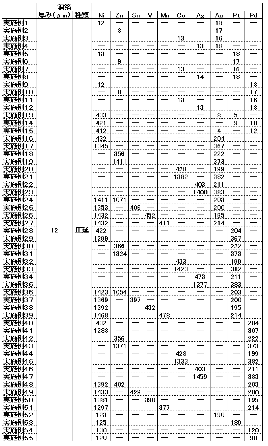
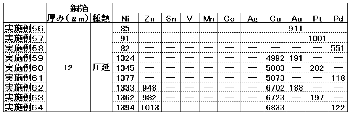
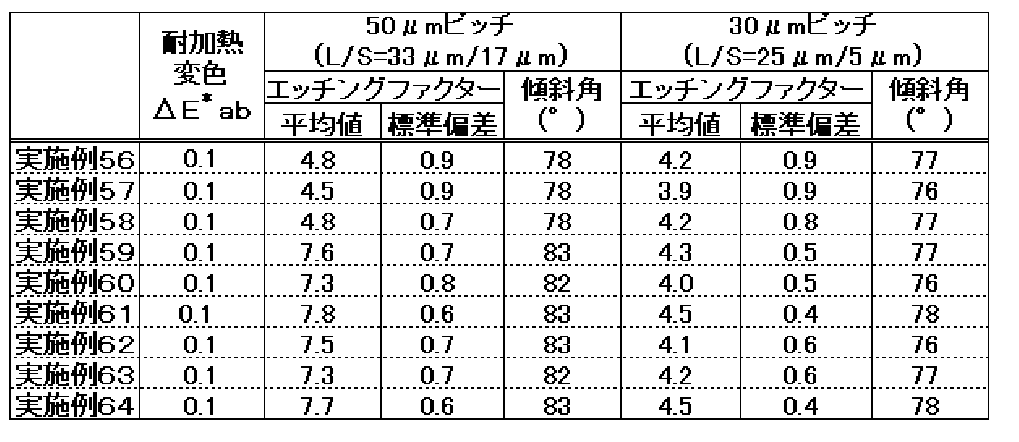
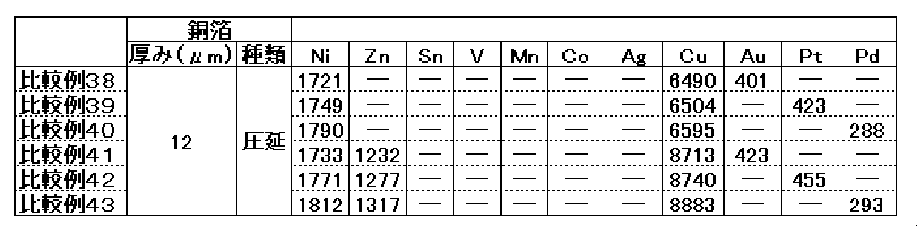
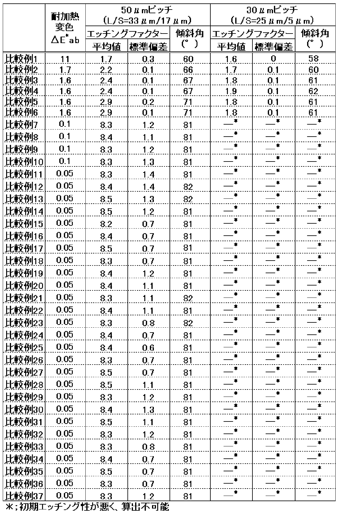
- the measurement results of Examples 1 to 4 are shown in Tables 1 to 8. In Tables 3, 4, 7, and 8, the standard of the color difference on the surface of the copper foil in each numerical range of the heat discoloration resistance ⁇ E * ab is shown below.
- Examples 1 to 64 In Examples 1 to 15, although a slight discoloration was observed, it was possible to form a circuit having a cross section close to a rectangular shape with a large etching factor and no variation with both 50 ⁇ m and 30 ⁇ m pitch resist patterns. . In Examples 16 to 64, almost no discoloration was observed, and a resist pattern with both 50 ⁇ m pitch and 30 ⁇ m pitch was able to form a circuit having a cross section close to a rectangular shape with a large etching factor and no variation. .
- Comparative Example 1 was a blank material with an untreated copper foil surface, and the sagging of the circuit increased with a resist pattern having a pitch of 50 ⁇ m and a pitch of 30 ⁇ m.
- Comparative Examples 2 to 6 since the adhesion amount of Ni, Zn, Sn, V or Mn in the first coating layer was insufficient, discoloration resistance was poor. Moreover, the 2nd coating layer was not formed and etching property was unsatisfactory. In Comparative Examples 7 to 10, the adhesion amount of Ni or the like in the first coating layer was excessive, the initial etching property was inferior (30 ⁇ m pitch), and the sagging of the circuit increased (50 ⁇ m pitch).
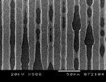
- FIG. 2 shows a photograph of the circuit formed in Comparative Example 13.
Landscapes
- Chemical & Material Sciences (AREA)
- Engineering & Computer Science (AREA)
- Chemical Kinetics & Catalysis (AREA)
- Materials Engineering (AREA)
- Mechanical Engineering (AREA)
- Metallurgy (AREA)
- Organic Chemistry (AREA)
- Microelectronics & Electronic Packaging (AREA)
- Parts Printed On Printed Circuit Boards (AREA)
- Manufacturing Of Printed Circuit Boards (AREA)
- Physical Vapour Deposition (AREA)
- Laminated Bodies (AREA)
Abstract
回路パターン形成の際のエッチング性が良好でファインピッチ化に適し、耐変色性が良好なプリント配線板用銅箔及びそれを用いた積層体を提供する。プリント配線板用銅箔は、銅箔基材と、銅箔基材の表面の少なくとも一部を被覆する被覆層を備える。被覆層は、Ni、Zn、Sn、V、Mn、Co及びAgの少なくともいずれか1種と、Pt、Pd、及び、Auの少なくともいずれか1種とを含む。
Description
本発明は、プリント配線板用銅箔及びそれを用いた積層体に関し、特にフレキシブルプリント配線板用の銅箔及びそれを用いた積層体に関する。
プリント配線板はここ半世紀に亘って大きな進展を遂げ、今日ではほぼすべての電子機器に使用されるまでに至っている。近年の電子機器の小型化、高性能化ニーズの増大に伴い搭載部品の高密度実装化や信号の高周波化が進展し、プリント配線板に対して導体パターンの微細化(ファインピッチ化)や高周波対応等が求められている。
プリント配線板は、銅箔に絶縁基板を接着、もしくは絶縁基板上にNi合金等を蒸着させた後に電気めっきで銅層を形成させて積層体とした後に、エッチングにより銅箔または銅層面に導体パターンを形成するという工程を経て製造されるのが一般的である。そのため、プリント配線板用の銅箔または銅層には良好なエッチング性が要求される。
銅箔は、樹脂との非接着面に表面処理を施さないと、エッチング後の銅箔回路の銅部分が、銅箔の表面から下に向かって、すなわち樹脂層に向かって、末広がりにエッチングされる(ダレを発生する)。通常は、回路側面の角度が小さい「ダレ」となり、特に大きな「ダレ」が発生した場合には、樹脂基板近傍で銅回路が短絡し、不良品となる場合もある。ここで、図3に、銅回路形成時に「ダレ」を生じて樹脂基板近傍で銅回路が短絡した例を示す回路表面の拡大写真を示す。
このような「ダレ」は極力小さくすることが必要であるが、このような末広がりのエッチング不良を防止するために、エッチング時間を延長して、エッチングをより多くして、この「ダレ」を減少させることも考えられる。しかし、この場合は、すでに所定の幅寸法に至っている箇所があると、そこがさらにエッチングされることになるので、その銅箔部分の回路幅がそれだけ狭くなり、回路設計上目的とする均一な線幅(回路幅)が得られず、特にその部分(細線化された部分)で発熱し、場合によっては断線するという問題が発生する。電子回路のファインパターン化がさらに進行する中で、現在もなお、このようなエッチング不良による問題がより強く現れ、回路形成上で、大きな問題となっている。
これらを改善する方法として、エッチング面側の銅箔に銅よりもエッチング速度が遅い金属又は合金層を形成した表面処理が特許文献1に開示されている。この場合の金属又は合金としては、Ni、Co及びこれらの合金である。回路設計に際しては、レジスト塗布側、すなわち銅箔の表面からエッチング液が浸透するので、レジスト直下にエッチング速度が遅い金属又は合金層があれば、その近傍の銅箔部分のエッチングが抑制され、他の銅箔部分のエッチングが進行するので、「ダレ」が減少し、より均一な幅の回路が形成できるという効果をもたらすという、従来技術と比較して急峻な回路形成が可能となり、大きな進歩があったと言える。
また、特許文献2では、厚さ1000~10000ÅのCu薄膜を形成し、該Cu薄膜の上に厚さ10~300Åの銅よりもエッチング速度が遅いNi薄膜を形成している。
近年、回路の微細化、高密度化がさらに進行し、より急峻に傾斜する側面を有する回路が求められている。しかしながら、特許文献1に記載される技術ではこれらには対応できない。
また、特許文献1に記載される表面処理層はソフトエッチングにより除去する必要があること、さらには樹脂との非接着面表面処理銅箔は、積層体に加工される工程で、樹脂の貼付け等の高温処理が施される。これは表面処理層の酸化を引き起こし、結果として銅箔のエッチング性は劣化する。
前者については、エッチング除去の時間をなるべく短縮し、きれいに除去するためには、表面処理層の厚さを極力薄くすることが必要であること、また後者の場合には、熱を受けるために、下地の銅層が酸化され(変色するので、通称「ヤケ」と言われている。)、レジストの塗布性(均一性、密着性)の不良やエッチング時の界面酸化物の過剰エッチングなどにより、パターンエッチングでのエッチング性、ショート、回路パターンの幅の制御性などの不良が発生するという問題があるので、改良が必要か又は他の材料に置換することが要求されている。
そこで、本発明は、回路パターン形成の際のエッチング性が良好でファインピッチ化に適し、耐変色性が良好なプリント配線板用銅箔及びそれを用いた積層体を提供することを課題とする。
本発明者らは、鋭意検討の結果、銅箔の樹脂との非接着面側に、Ni等と、Pt、Pd、及び、Auのいずれか1種以上とを含む被覆層を設けた場合には、回路側面の傾斜角が80°以上となるような回路を形勢でき、さらに銅箔表面の耐変色性が良好となることを見出した。
以上の知見を基礎として完成した本発明は一側面において、銅箔基材と、銅箔基材の表面の少なくとも一部を被覆する被覆層を備え、被覆層は、Ni、Zn、Sn、V、Mn、Co及びAgの少なくともいずれか1種と、Pt、Pd、及び、Auの少なくともいずれか1種とを含むプリント配線板用銅箔である。
本発明に係るプリント配線板用銅箔の一実施形態においては、被覆層は、Ni、Zn、Sn、V、Mn、Co及びAgのいずれか1種以上を含む第1の被覆層と、Pt、Pd、及び、Auのいずれか1種以上を含む第2の被覆層とで形成されている。
本発明に係るプリント配線板用銅箔の別の一実施形態においては、前記第1の被覆層が、被覆量が1500μg/dm2以下のNi、Co、Ag及びZnのいずれか1種からなる。
本発明に係るプリント配線板用銅箔の更に別の一実施形態においては、前記第1の被覆層が、被覆量が1500μg/dm2以下のNi及び1100μg/dm2以下のZnからなるNi-Zn合金、被覆量が1500μg/dm2以下のNi及び500μg/dm2以下のSnからなるNi-Sn合金、被覆量が1500μg/dm2以下のNi及び500μg/dm2以下のVからなるNi-V合金、又は、被覆量が1500μg/dm2以下のNi及び500μg/dm2以下のMnからなるNi-Mn合金、又は、被覆量が1500μg/dm2以下のNi及び1100μg/dm2以下のZnからなるNi-Cu-Zn合金、又は、被覆量が1500μg/dm2以下のNiからなるNi-Cu合金からなる。
本発明に係るプリント配線板用銅箔の更に別の一実施形態においては、前記第2の被覆層におけるPtの付着量が1050μg/dm2以下、Pdの付着量が600μg/dm2以下、Auの付着量が1000μg/dm2以下である。
本発明に係るプリント配線板用銅箔の更に別の一実施形態においては、前記第2の被覆層におけるPtの付着量が20~400μg/dm2、Pdの付着量が20~250μg/dm2、Auの付着量が20~400μg/dm2である。
本発明に係るプリント配線板用銅箔の更に別の一実施形態においては、前記第2の被覆層におけるPtの付着量が50~300μg/dm2、Pdの付着量が30~180μg/dm2、Auの付着量が50~300μg/dm2である。
本発明に係るプリント配線板用銅箔の更に別の一実施形態においては、第1の被覆層が銅箔基材の表面に形成され、第2の被覆層が第1の被覆層上に形成されている。
本発明に係るプリント配線板用銅箔の更に別の一実施形態においては、第2の被覆層が銅箔基材の表面に形成され、第1の被覆層が第2の被覆層上に形成されている。
本発明に係るプリント配線板用銅箔の更に別の一実施形態においては、プリント配線板はフレキシブルプリント配線板である。
本発明は別の一側面において、本発明に係る銅箔で構成された圧延銅箔又は電解銅箔を準備する工程と、銅箔の被覆層をエッチング面として該銅箔と樹脂基板との積層体を作製する工程と、積層体を塩化第二鉄水溶液又は塩化第二銅水溶液を用いてエッチングし、銅の不必要部分を除去して銅の回路を形成する工程とを含む電子回路の形成方法である。
本発明は更に別の一側面において、本発明に係る銅箔と樹脂基板との積層体である。
本発明は更に別の一側面において、銅層と樹脂基板との積層体であって、銅層の表面の少なくとも一部を被覆する本発明に係る被覆層を備えた積層体である。
本発明に係る積層体の一実施形態においては、銅箔がポリイミドに接着している構造を有する。
本発明は更に別の一側面において、本発明に係る積層体を材料としたプリント配線板である。
本発明によれば、回路パターン形成の際のエッチング性が良好でファインピッチ化に適し、耐変色性が良好なプリント配線板用銅箔及びそれを用いた積層体を提供することができる。
(銅箔基材)
本発明に用いることのできる銅箔基材の形態に特に制限はないが、典型的には圧延銅箔や電解銅箔の形態で用いることができる。一般的には、電解銅箔は硫酸銅めっき浴からチタンやステンレスのドラム上に銅を電解析出して製造され、圧延銅箔は圧延ロールによる塑性加工と熱処理を繰り返して製造される。屈曲性が要求される用途には圧延銅箔を適用することが多い。
銅箔基材の材料としてはプリント配線板の導体パターンとして通常使用されるタフピッチ銅や無酸素銅といった高純度の銅の他、例えばSn入り銅、Ag入り銅、Cr、Zr又はMg等を添加した銅合金、Ni及びSi等を添加したコルソン系銅合金のような銅合金も使用可能である。なお、本明細書において用語「銅箔」を単独で用いたときには銅合金箔も含むものとする。
本発明に用いることのできる銅箔基材の形態に特に制限はないが、典型的には圧延銅箔や電解銅箔の形態で用いることができる。一般的には、電解銅箔は硫酸銅めっき浴からチタンやステンレスのドラム上に銅を電解析出して製造され、圧延銅箔は圧延ロールによる塑性加工と熱処理を繰り返して製造される。屈曲性が要求される用途には圧延銅箔を適用することが多い。
銅箔基材の材料としてはプリント配線板の導体パターンとして通常使用されるタフピッチ銅や無酸素銅といった高純度の銅の他、例えばSn入り銅、Ag入り銅、Cr、Zr又はMg等を添加した銅合金、Ni及びSi等を添加したコルソン系銅合金のような銅合金も使用可能である。なお、本明細書において用語「銅箔」を単独で用いたときには銅合金箔も含むものとする。
本発明に用いることのできる銅箔基材の厚さについても特に制限はなく、プリント配線板用に適した厚さに適宜調節すればよい。例えば、5~100μm程度とすることができる。但し、ファインパターン形成を目的とする場合には30μm以下、好ましくは20μm以下であり、典型的には5~20μm程度である。
本発明に使用する銅箔基材は、特に限定されないが、例えば、粗化処理をしないものを用いても良い。従来は特殊めっきで表面にμmオーダーの凹凸を付けて表面粗化処理を施し、物理的なアンカー効果によって樹脂との接着性を持たせるケースが一般的であるが、一方でファインピッチや高周波電気特性は平滑な箔が良いとされ、粗化箔では不利な方向に働くことがある。また、粗化処理をしないものであると、粗化処理工程が省略されるので、経済性・生産性向上の効果がある。
(1)被覆層の構成
銅箔基材の絶縁基板との接着面の反対側(回路形成予定面側)の表面の少なくとも一部には、被覆層が形成されている。被覆層は、Ni、Zn、Sn、V、Mn、Co及びAgの少なくともいずれか1種と、Pt、Pd、及び、Auの少なくともいずれか1種とを含む。被覆層は、Ni、Zn、Sn、V、Mn、Co及びAgのいずれか1種以上を含む第1の被覆層と、Pt、Pd、及び、Auのいずれか1種以上を含む第2の被覆層とで形成されていてもよい。また、この場合、第1の被覆層は、被覆量が1500μg/dm2以下のNi、Co、Ag及びZnのいずれか1種で構成されてもよい。さらに、第1の被覆層は、被覆量が1500μg/dm2以下のNi及び1100μg/dm2以下のZnからなるNi-Zn合金、被覆量が1500μg/dm2以下のNi及び500μg/dm2以下のSnからなるNi-Sn合金、被覆量が1500μg/dm2以下のNi及び500μg/dm2以下のVからなるNi-V合金、又は、被覆量が1500μg/dm2以下のNi及び500μg/dm2以下のMnからなるNi-Mn合金、又は、被覆量が1500μg/dm2以下のNi及び1100μg/dm2以下のZnからなるNi-Cu-Zn合金、又は、被覆量が1500μg/dm2以下のNiからなるNi-Cu合金で構成されていてもよい。このように、第1の被覆層がNi、Co、Ag及びZnの中でも特にNiを含有する合金で構成されていると、初期エッチング性がより良好となり、好ましい。各金属の付着量が上述の数値範囲未満であると初期エッチング性や耐変色性に悪影響を及ぼし、上述の数値範囲を超えると、回路のダレが大きくなり直線性が不良となる。
銅箔基材の絶縁基板との接着面の反対側(回路形成予定面側)の表面の少なくとも一部には、被覆層が形成されている。被覆層は、Ni、Zn、Sn、V、Mn、Co及びAgの少なくともいずれか1種と、Pt、Pd、及び、Auの少なくともいずれか1種とを含む。被覆層は、Ni、Zn、Sn、V、Mn、Co及びAgのいずれか1種以上を含む第1の被覆層と、Pt、Pd、及び、Auのいずれか1種以上を含む第2の被覆層とで形成されていてもよい。また、この場合、第1の被覆層は、被覆量が1500μg/dm2以下のNi、Co、Ag及びZnのいずれか1種で構成されてもよい。さらに、第1の被覆層は、被覆量が1500μg/dm2以下のNi及び1100μg/dm2以下のZnからなるNi-Zn合金、被覆量が1500μg/dm2以下のNi及び500μg/dm2以下のSnからなるNi-Sn合金、被覆量が1500μg/dm2以下のNi及び500μg/dm2以下のVからなるNi-V合金、又は、被覆量が1500μg/dm2以下のNi及び500μg/dm2以下のMnからなるNi-Mn合金、又は、被覆量が1500μg/dm2以下のNi及び1100μg/dm2以下のZnからなるNi-Cu-Zn合金、又は、被覆量が1500μg/dm2以下のNiからなるNi-Cu合金で構成されていてもよい。このように、第1の被覆層がNi、Co、Ag及びZnの中でも特にNiを含有する合金で構成されていると、初期エッチング性がより良好となり、好ましい。各金属の付着量が上述の数値範囲未満であると初期エッチング性や耐変色性に悪影響を及ぼし、上述の数値範囲を超えると、回路のダレが大きくなり直線性が不良となる。
第2の被覆層において、Ptの付着量が1050μg/dm2以下、Pdの付着量が600μg/dm2以下、Auの付着量が1000μg/dm2以下であるのが好ましい。これらの値を超えると、それぞれ初期エッチング性に悪影響を及ぼすためである。また、Ptの付着量が20~400μg/dm2、Pdの付着量が20~250μg/dm2、Auの付着量が20~400μg/dm2であるのがより好ましい。被覆層のPtの付着量が20μg/dm2以上、被覆層のPdの付着量が20μg/dm2以上、及び、被覆層のAuの付着量が20μg/dm2以上であると、それぞれ効果がより良好となる。なお、Ptの付着量が50~300μg/dm2、Pdの付着量が30~180μg/dm2、Auの付着量が50~300μg/dm2であるのが更により好ましい。
また、上述の第1の被覆層及び第2の被覆層の形成順はいずれが先であってもよい。すなわち、第1の被覆層が銅箔基材の表面に形成され、第2の被覆層が第1の被覆層上に形成されていてもよく、第2の被覆層が銅箔基材の表面に形成され、第1の被覆層が第2の被覆層上に形成されていてもよい。
さらに、被覆層上には、防錆効果を高めるためにさらにクロム層若しくはクロメート層及び又はシラン処理層を形成することができる。
(銅箔の製造方法)
本発明に係るプリント配線板用銅箔は、スパッタリング法により形成することができる。すなわち、スパッタリング法によって銅箔基材の表面の少なくとも一部を、Ni、Zn、Sn、V、Mn、Co及びAgの少なくともいずれか1種と、Pt、Pd、及び、Auの少なくともいずれか1種との合金で構成された被覆層で被覆することができる。また、スパッタリング法によって銅箔基材の表面の少なくとも一部に、Ni等からなる第1の被覆層を形成した後、さらに銅よりもエッチングレートの低いPt、Pd、及び、Auのいずれか1種以上からなる第2の被覆層を形成してもよい。さらに、スパッタリング法によって銅箔基材の表面の少なくとも一部に、銅よりもエッチングレートの低いPt、Pd、及び、Auのいずれか1種以上からなる第2の被覆層を形成した後、さらにNi等からなる第1の被覆層を形成してもよい。第1及び第2の被覆層は、スパッタリング法に限らず、例えば、電気めっき、無電解めっき等の湿式めっき法で形成してもよい。
本発明に係るプリント配線板用銅箔は、スパッタリング法により形成することができる。すなわち、スパッタリング法によって銅箔基材の表面の少なくとも一部を、Ni、Zn、Sn、V、Mn、Co及びAgの少なくともいずれか1種と、Pt、Pd、及び、Auの少なくともいずれか1種との合金で構成された被覆層で被覆することができる。また、スパッタリング法によって銅箔基材の表面の少なくとも一部に、Ni等からなる第1の被覆層を形成した後、さらに銅よりもエッチングレートの低いPt、Pd、及び、Auのいずれか1種以上からなる第2の被覆層を形成してもよい。さらに、スパッタリング法によって銅箔基材の表面の少なくとも一部に、銅よりもエッチングレートの低いPt、Pd、及び、Auのいずれか1種以上からなる第2の被覆層を形成した後、さらにNi等からなる第1の被覆層を形成してもよい。第1及び第2の被覆層は、スパッタリング法に限らず、例えば、電気めっき、無電解めっき等の湿式めっき法で形成してもよい。
(プリント配線板の製造方法)
本発明に係る銅箔を用いてプリント配線板(PWB)を常法に従って製造することができる。以下に、プリント配線板の製造方法の例を示す。
本発明に係る銅箔を用いてプリント配線板(PWB)を常法に従って製造することができる。以下に、プリント配線板の製造方法の例を示す。
まず、銅箔と絶縁基板とを貼り合わせて積層体を製造する。銅箔が積層される絶縁基板はプリント配線板に適用可能な特性を有するものであれば特に制限を受けないが、例えば、リジッドPWB用に紙基材フェノール樹脂、紙基材エポキシ樹脂、合成繊維布基材エポキシ樹脂、ガラス布・紙複合基材エポキシ樹脂、ガラス布・ガラス不織布複合基材エポキシ樹脂及びガラス布基材エポキシ樹脂等を使用し、FPC用にポリエステルフィルムやポリイミドフィルム等を使用する事ができる。
貼り合わせの方法は、リジッドPWB用の場合、ガラス布などの基材に樹脂を含浸させ、樹脂を半硬化状態まで硬化させたプリプレグを用意する。銅箔を被覆層の反対側の面からプリプレグに重ねて加熱加圧させることにより行うことができる。
フレキシブルプリント配線板(FPC)用の場合、ポリイミドフィルム又はポリエステルフィルムと銅箔とをエポキシ系やアクリル系の接着剤を使って接着することができる(3層構造)。また、接着剤を使用しない方法(2層構造)としては、ポリイミドの前駆体であるポリイミドワニス(ポリアミック酸ワニス)を銅箔に塗布し、加熱することでイミド化するキャスティング法や、ポリイミドフィルム上に熱可塑性のポリイミドを塗布し、その上に銅箔を重ね合わせ、加熱加圧するラミネート法が挙げられる。キャスティング法においては、ポリイミドワニスを塗布する前に熱可塑性ポリイミド等のアンカーコート材を予め塗布しておくことも有効である。
本発明に係る積層体は各種のプリント配線板(PWB)に使用可能であり、特に制限されるものではないが、例えば、導体パターンの層数の観点からは片面PWB、両面PWB、多層PWB(3層以上)に適用可能であり、絶縁基板材料の種類の観点からはリジッドPWB、フレキシブルPWB(FPC)、リジッド・フレックスPWBに適用可能である。また、本発明に係る積層体は、銅箔を樹脂に貼り付けてなる上述のような銅張積層板に限定されず、樹脂上にスパッタリング、めっきで銅層を形成したメタライジング材であってもよい。
上述のように作製した銅箔積層板は、銅箔表面にNi等を含む被覆層を備えているため、高温の熱処理によっても変色され難く、外観が良好である。
上述のように作製した積層体の銅箔上に形成された被覆層表面にレジストを塗布し、マスクによりパターンを露光し、現像することによりレジストパターンを形成したものをエッチング液に浸漬する。このとき、Pt、Pd、及び、Auのいずれか1種以上を含む第2の被覆層は、銅箔上のレジスト部分に近い位置にあり、レジスト側の銅箔のエッチングは、この第2の被覆層近傍がエッチングされていく速度よりも速い速度で、第2の被覆層から離れた部位の銅のエッチングが進行することにより、銅の回路パターンのエッチングがほぼ垂直に進行する。これにより銅の不必要部分を除去されて、次いでエッチングレジストを剥離・除去して回路パターンを露出することができる。
積層体に回路パターンを形成するために用いるエッチング液に対しては、第2の被覆層のエッチング速度は、銅よりも十分に小さいためエッチングファクターを改善する効果を有する。エッチング液は、塩化第二銅水溶液、又は、塩化第二鉄水溶液等を用いることができるが、特に塩化第二鉄水溶液が有効である。微細回路はエッチングに時間が掛かるが、塩化第二鉄水溶液の方が塩化第二銅水溶液よりもエッチング速度が早いためである。また、被覆層を形成する前に、あらかじめ銅箔基材表面に耐熱層を形成しておいてもよい。
積層体に回路パターンを形成するために用いるエッチング液に対しては、第2の被覆層のエッチング速度は、銅よりも十分に小さいためエッチングファクターを改善する効果を有する。エッチング液は、塩化第二銅水溶液、又は、塩化第二鉄水溶液等を用いることができるが、特に塩化第二鉄水溶液が有効である。微細回路はエッチングに時間が掛かるが、塩化第二鉄水溶液の方が塩化第二銅水溶液よりもエッチング速度が早いためである。また、被覆層を形成する前に、あらかじめ銅箔基材表面に耐熱層を形成しておいてもよい。
(プリント配線板の銅箔表面の回路のラインパターン形状)
上述のように被覆層側からエッチングされて形成されたプリント配線板の銅箔表面の回路の各ラインパターンは、その長尺状の2つの側面が絶縁基板上に垂直に形成されるのではなく、通常、銅箔の表面から下に向かって、すなわち樹脂層に向かって、末広がりに形成される(ダレの発生)。これにより、長尺状の2つの側面はそれぞれ絶縁基板表面に対して傾斜角θを有している。現在要求されている回路パターンの微細化(ファインピッチ化)のためには、ラインパターンのピッチをなるべく狭くすることが重要であるが、この傾斜角θが小さいと、それだけダレが大きくなり、ラインパターンのピッチが広くなってしまう。また、傾斜角θは、通常、各ラインパターン及びラインパターン内で完全に一定ではない。このような傾斜角θのばらつきが大きいと、回路の品質に悪影響を及ぼすおそれがある。従って、被覆層側からエッチングされて形成されたプリント配線板の銅箔表面の回路の各ラインパターンは、長尺状の2つの側面がそれぞれ絶縁基板表面に対して65~90°の傾斜角θを有し、且つ、同一回路内のtanθの標準偏差が1.0以下であるのが望ましい。
上述のように被覆層側からエッチングされて形成されたプリント配線板の銅箔表面の回路の各ラインパターンは、その長尺状の2つの側面が絶縁基板上に垂直に形成されるのではなく、通常、銅箔の表面から下に向かって、すなわち樹脂層に向かって、末広がりに形成される(ダレの発生)。これにより、長尺状の2つの側面はそれぞれ絶縁基板表面に対して傾斜角θを有している。現在要求されている回路パターンの微細化(ファインピッチ化)のためには、ラインパターンのピッチをなるべく狭くすることが重要であるが、この傾斜角θが小さいと、それだけダレが大きくなり、ラインパターンのピッチが広くなってしまう。また、傾斜角θは、通常、各ラインパターン及びラインパターン内で完全に一定ではない。このような傾斜角θのばらつきが大きいと、回路の品質に悪影響を及ぼすおそれがある。従って、被覆層側からエッチングされて形成されたプリント配線板の銅箔表面の回路の各ラインパターンは、長尺状の2つの側面がそれぞれ絶縁基板表面に対して65~90°の傾斜角θを有し、且つ、同一回路内のtanθの標準偏差が1.0以下であるのが望ましい。
以下、本発明の実施例を示すが、これらは本発明をより良く理解するために提供するものであり、本発明が限定されることを意図するものではない。
(例1:実施例1~54、56~64)
(銅箔への被覆層の形成)
実施例1~54、56~64の銅箔基材として、厚さ12μmの圧延銅箔(日鉱金属製C1100)を用意した。
(銅箔への被覆層の形成)
実施例1~54、56~64の銅箔基材として、厚さ12μmの圧延銅箔(日鉱金属製C1100)を用意した。
銅箔の表面に付着している薄い酸化膜を逆スパッタにより取り除き、Ni等の各ターゲットを以下の装置及び条件でスパッタリングすることにより第1の被覆層を形成した後、さらにPt、Pd、Auのターゲットを以下の装置及び条件でスパッタリングすることにより、第2の被覆層を形成した。被覆層の厚さは成膜時間を調整することにより変化させた。スパッタリングに使用した各種金属の単体は純度が3Nのものを用いた。
・装置:バッチ式スパッタリング装置(アルバック社、型式MNS-6000)
・到達真空度:1.0×10⁻⁵Pa
・スパッタリング圧:0.2Pa
・逆スパッタ電力:100W
・スパッタリング電力:50W
・成膜速度:各ターゲットについて一定時間約0.2μm成膜し、3次元測定器で厚さを測定し、単位時間当たりのスパッタレートを算出した。
上記実施例のうち、実施例13~15については、以下のターゲットを用いた。
・ターゲット:Au-50質量%Pd、Pt-50質量%Pd、Au-50質量%Pt
上記実施例のうち、実施例52~54については、以下のターゲットを用いた。
・ターゲット:Au-50質量%Ni、Pt-50質量%Ni、Pd-50質量%Ni
上記実施例のうち、実施例59~61については、以下のターゲットを用いた。
・ターゲット:Ni-80質量%Cu、及び、純度3NのAu、Pt又はPd
上記実施例のうち、実施例62~64については、以下のターゲットを用いた。
・ターゲット:Ni-64質量%Cu-18質量%Zn、及び、純度3NのAu、Pt又はPd
・装置:バッチ式スパッタリング装置(アルバック社、型式MNS-6000)
・到達真空度:1.0×10⁻⁵Pa
・スパッタリング圧:0.2Pa
・逆スパッタ電力:100W
・スパッタリング電力:50W
・成膜速度:各ターゲットについて一定時間約0.2μm成膜し、3次元測定器で厚さを測定し、単位時間当たりのスパッタレートを算出した。
上記実施例のうち、実施例13~15については、以下のターゲットを用いた。
・ターゲット:Au-50質量%Pd、Pt-50質量%Pd、Au-50質量%Pt
上記実施例のうち、実施例52~54については、以下のターゲットを用いた。
・ターゲット:Au-50質量%Ni、Pt-50質量%Ni、Pd-50質量%Ni
上記実施例のうち、実施例59~61については、以下のターゲットを用いた。
・ターゲット:Ni-80質量%Cu、及び、純度3NのAu、Pt又はPd
上記実施例のうち、実施例62~64については、以下のターゲットを用いた。
・ターゲット:Ni-64質量%Cu-18質量%Zn、及び、純度3NのAu、Pt又はPd
被覆層を設けた銅箔に対して、被覆層と反対側の表面にあらかじめ付着している薄い酸化被膜を逆スパッタリングによって取り除き、Ni層及びCr層を順に成膜した。
上記手順で表面処理が施された銅箔に、接着剤付ポリイミドフィルム(ニッカン工業製、CISV1215)を7kgf/cm2の圧力、160℃で40分間の加熱プレスで積層させた。一部の銅箔は、窒素雰囲気下で350℃で2時間保持した後に、上記手順でポリイミドフィルムと積層させた。
上記手順で表面処理が施された銅箔に、接着剤付ポリイミドフィルム(ニッカン工業製、CISV1215)を7kgf/cm2の圧力、160℃で40分間の加熱プレスで積層させた。一部の銅箔は、窒素雰囲気下で350℃で2時間保持した後に、上記手順でポリイミドフィルムと積層させた。
<付着量の測定>
第1の被覆層の各金属の付着量は、50mm×50mmの銅箔表面の被膜をHNO3(2重量%)とHCl(5重量%)を混合した溶液に溶解し、その溶液中の金属濃度をICP発光分光分析装置(エスアイアイ・ナノテクノロジー株式会社製、SFC-3100)にて定量し、単位面積当たりの金属量(μg/dm2)を算出した。
第2の被覆層のAu、Pd、Ptの付着量測定は、王水で表面処理銅箔サンプルを溶解させ、その溶解液を希釈し、原子吸光分析法で行った。
第1の被覆層の各金属の付着量は、50mm×50mmの銅箔表面の被膜をHNO3(2重量%)とHCl(5重量%)を混合した溶液に溶解し、その溶液中の金属濃度をICP発光分光分析装置(エスアイアイ・ナノテクノロジー株式会社製、SFC-3100)にて定量し、単位面積当たりの金属量(μg/dm2)を算出した。
第2の被覆層のAu、Pd、Ptの付着量測定は、王水で表面処理銅箔サンプルを溶解させ、その溶解液を希釈し、原子吸光分析法で行った。
(エッチングによる回路形状)
銅箔のエッチング面をアセトンで脱脂し、硫酸(100g/L)に30秒浸漬させて、表面の汚れ及び酸化層を取り除いた。次に、スピンコーターを用いて液体レジスト(東京応化工業製、OFPR-800LB)をエッチング面に滴下し、乾燥させた。乾燥後のレジスト厚みは1μmとなるように調整した。その後、露光工程により10本の回路を印刷し、さらに銅箔の不要部分を除去するエッチング処理を以下の条件で実施した。
銅箔のエッチング面をアセトンで脱脂し、硫酸(100g/L)に30秒浸漬させて、表面の汚れ及び酸化層を取り除いた。次に、スピンコーターを用いて液体レジスト(東京応化工業製、OFPR-800LB)をエッチング面に滴下し、乾燥させた。乾燥後のレジスト厚みは1μmとなるように調整した。その後、露光工程により10本の回路を印刷し、さらに銅箔の不要部分を除去するエッチング処理を以下の条件で実施した。
<エッチング条件>
・塩化第二鉄水溶液:(37wt%、ボーメ度:40°)
・液温:50℃
・スプレー圧:0.25MPa
(50μmピッチ回路形成)
・レジストL/S=33μm/17μm
・仕上がり回路ボトム(底部)幅:25μm
・エッチング時間:10~130秒
(30μmピッチ回路形成)
・レジストL/S=25μm/5μm
・仕上がり回路ボトム(底部)幅:15μm
・エッチング時間:30~70秒
・エッチング終点の確認:時間を変えてエッチングを数水準行い、光学顕微鏡で回路間に銅が残存しなくなるのを確認し、これをエッチング時間とした。
エッチング後、45℃のNaOH水溶液(100g/L)に1分間浸漬させてレジストを剥離した。
・塩化第二鉄水溶液:(37wt%、ボーメ度:40°)
・液温:50℃
・スプレー圧:0.25MPa
(50μmピッチ回路形成)
・レジストL/S=33μm/17μm
・仕上がり回路ボトム(底部)幅:25μm
・エッチング時間:10~130秒
(30μmピッチ回路形成)
・レジストL/S=25μm/5μm
・仕上がり回路ボトム(底部)幅:15μm
・エッチング時間:30~70秒
・エッチング終点の確認:時間を変えてエッチングを数水準行い、光学顕微鏡で回路間に銅が残存しなくなるのを確認し、これをエッチング時間とした。
エッチング後、45℃のNaOH水溶液(100g/L)に1分間浸漬させてレジストを剥離した。
<エッチングファクターの測定条件>
エッチングファクターは、末広がりにエッチングされた場合(ダレが発生した場合)、回路が垂直にエッチングされたと仮定した場合の、銅箔上面からの垂線と樹脂基板との交点からのダレの長さの距離をaとした場合において、このaと銅箔の厚さbとの比:b/aを示すものであり、この数値が大きいほど、傾斜角は大きくなり、エッチング残渣が残らず、ダレが小さくなることを意味する。図1に、回路パターンの一部の表面写真と、当該部分における回路パターンの幅方向の横断面の模式図と、該模式図を用いたエッチングファクターの計算方法の概略とを示す。このaは回路上方からのSEM観察により測定し、エッチングファクター(EF=b/a)を算出した。このエッチングファクターを用いることにより、エッチング性の良否を簡単に判定できる。さらに、傾斜角θは上記手順で測定したa及び銅箔の厚さbを用いてアークタンジェントを計算することにより算出した。これらの測定範囲は回路長600μmで、12点のエッチングファクター、その標準偏差及び傾斜角θの平均値を結果として採用した。
エッチングファクターは、末広がりにエッチングされた場合(ダレが発生した場合)、回路が垂直にエッチングされたと仮定した場合の、銅箔上面からの垂線と樹脂基板との交点からのダレの長さの距離をaとした場合において、このaと銅箔の厚さbとの比:b/aを示すものであり、この数値が大きいほど、傾斜角は大きくなり、エッチング残渣が残らず、ダレが小さくなることを意味する。図1に、回路パターンの一部の表面写真と、当該部分における回路パターンの幅方向の横断面の模式図と、該模式図を用いたエッチングファクターの計算方法の概略とを示す。このaは回路上方からのSEM観察により測定し、エッチングファクター(EF=b/a)を算出した。このエッチングファクターを用いることにより、エッチング性の良否を簡単に判定できる。さらに、傾斜角θは上記手順で測定したa及び銅箔の厚さbを用いてアークタンジェントを計算することにより算出した。これらの測定範囲は回路長600μmで、12点のエッチングファクター、その標準偏差及び傾斜角θの平均値を結果として採用した。
<耐変色試験方法>
耐変色加熱性は、恒温槽を用いて300℃10分の条件で加熱後、色彩色差計を用いてL*(明るさ)、a*(赤-緑軸の色度)、b*(黄-青軸の色度)を測定し、(JIS Z 8729)に基づいて、式(1)に示すΔE*abにより評価した。
ΔE*ab=[(ΔL*)2+(Δa*)2+(Δb*)2]1/2
耐変色加熱性は、恒温槽を用いて300℃10分の条件で加熱後、色彩色差計を用いてL*(明るさ)、a*(赤-緑軸の色度)、b*(黄-青軸の色度)を測定し、(JIS Z 8729)に基づいて、式(1)に示すΔE*abにより評価した。
ΔE*ab=[(ΔL*)2+(Δa*)2+(Δb*)2]1/2
(例2:実施例55)
12μm厚の圧延銅箔を用意し、銅箔の表面に付着している薄い酸化膜を逆スパッタにより取り除き、Pdターゲットをスパッタリングすることにより第1の被覆層を形成し、次にNiターゲットをスパッタリングすることにより第二の被覆層を形成した。その後、同様の手順でポリイミドフィルムを接着した。次に、反対面に感光性レジスト塗布及び露光工程により10本の回路を印刷し、さらに銅箔の不要部分を除去するエッチング処理を例1の条件で実施した。
12μm厚の圧延銅箔を用意し、銅箔の表面に付着している薄い酸化膜を逆スパッタにより取り除き、Pdターゲットをスパッタリングすることにより第1の被覆層を形成し、次にNiターゲットをスパッタリングすることにより第二の被覆層を形成した。その後、同様の手順でポリイミドフィルムを接着した。次に、反対面に感光性レジスト塗布及び露光工程により10本の回路を印刷し、さらに銅箔の不要部分を除去するエッチング処理を例1の条件で実施した。
(例3:比較例1:ブランク材)
12μm厚の圧延銅箔を準備し、例1と同じ手順でポリイミドフィルムを接着した。次に反対面に感光性レジスト塗布及び露光工程により10本の回路を印刷し、さらに銅箔の不要部分を除去するエッチング処理を例1の条件で実施した。
12μm厚の圧延銅箔を準備し、例1と同じ手順でポリイミドフィルムを接着した。次に反対面に感光性レジスト塗布及び露光工程により10本の回路を印刷し、さらに銅箔の不要部分を除去するエッチング処理を例1の条件で実施した。
(例4:比較例2~43)
12μm厚の圧延銅箔を準備し、例1と同じ手順で樹脂との接着面側を表面処理した後、ポリイミドフィルムを接着した。次に、銅箔表面に例1と同様にNi等で構成された第1の被覆層、Pt、Pd、Auで構成された第2の被覆層をそれぞれスパッタリングで形成し、エッチングで回路を形成した。
例1~4の各測定結果を表1~8に示す。表3、4、7及び8において、耐加熱変色ΔE*abの各数値範囲における銅箔表面の色差の基準を以下に示す。
ΔE*ab=0~0.5 極めてわずかに異なる(trace)
ΔE*ab=0.5~1.5 わずかに異なる(slight)
ΔE*ab=1.5~3.0 感知し得るほどに異なる(noticiable)
ΔE*ab=3.0~6.0 著しく異なる(appreciable)
ΔE*ab=6.0~12.0 極めて著しく異なる(much)
ΔE*ab=12.0超 別の色系統になる(very much)
12μm厚の圧延銅箔を準備し、例1と同じ手順で樹脂との接着面側を表面処理した後、ポリイミドフィルムを接着した。次に、銅箔表面に例1と同様にNi等で構成された第1の被覆層、Pt、Pd、Auで構成された第2の被覆層をそれぞれスパッタリングで形成し、エッチングで回路を形成した。
例1~4の各測定結果を表1~8に示す。表3、4、7及び8において、耐加熱変色ΔE*abの各数値範囲における銅箔表面の色差の基準を以下に示す。
ΔE*ab=0~0.5 極めてわずかに異なる(trace)
ΔE*ab=0.5~1.5 わずかに異なる(slight)
ΔE*ab=1.5~3.0 感知し得るほどに異なる(noticiable)
ΔE*ab=3.0~6.0 著しく異なる(appreciable)
ΔE*ab=6.0~12.0 極めて著しく異なる(much)
ΔE*ab=12.0超 別の色系統になる(very much)

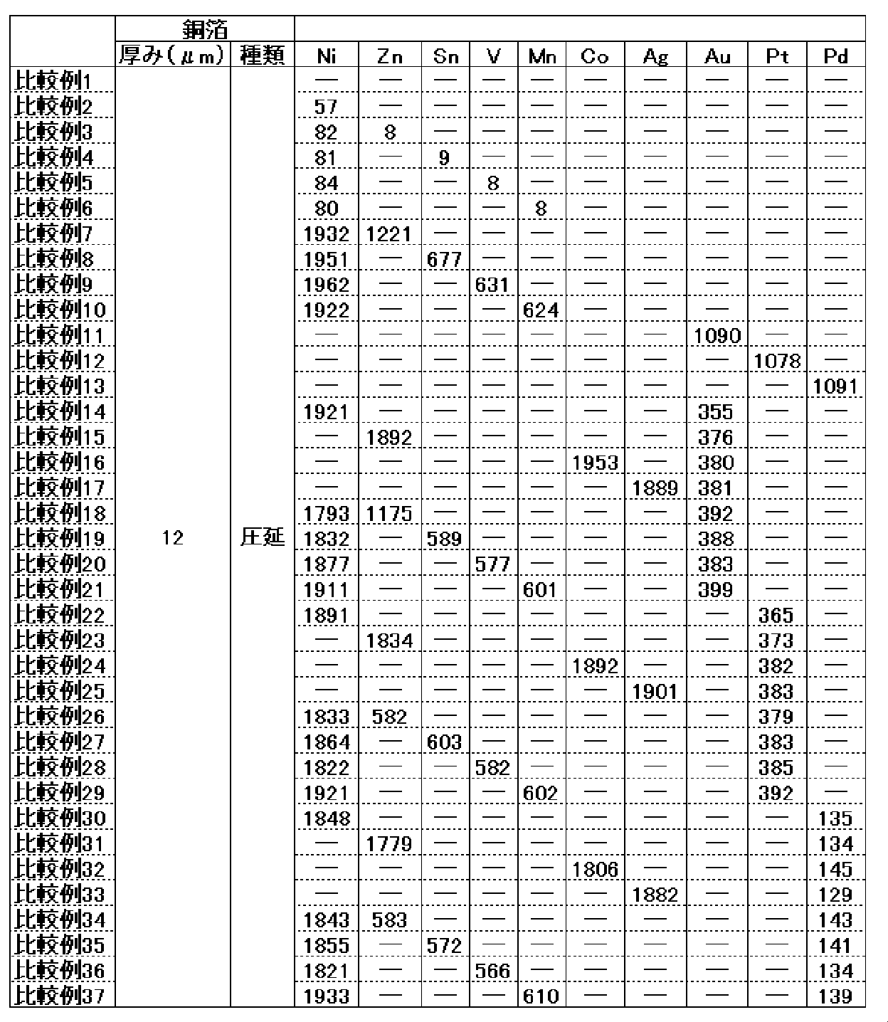

<評価>
(実施例1~64)
実施例1~15では、やや変色が見られたものの、50μmピッチ及び30μmピッチの両方のレジストパターンで、エッチングファクターが大きく且つバラツキもなく、矩形方に近い断面の回路を形成することができた。実施例16~64では、変色もほとんど見られず、さらに50μmピッチ及び30μmピッチの両方のレジストパターンで、エッチングファクターが大きく且つバラツキもなく、矩形方に近い断面の回路を形成することができた。
(実施例1~64)
実施例1~15では、やや変色が見られたものの、50μmピッチ及び30μmピッチの両方のレジストパターンで、エッチングファクターが大きく且つバラツキもなく、矩形方に近い断面の回路を形成することができた。実施例16~64では、変色もほとんど見られず、さらに50μmピッチ及び30μmピッチの両方のレジストパターンで、エッチングファクターが大きく且つバラツキもなく、矩形方に近い断面の回路を形成することができた。
(比較例1~43)
比較例1は、銅箔表面が未処理であるブランク材であり、50μmピッチ、30μmピッチのレジストパターンで回路のダレが大きくなった。
比較例2~6では、第1の被覆層中のNi、Zn、Sn、V又はMnの付着量が不足したため、耐変色性が不良となった。また、第2の被覆層を形成しておらず、エッチング性が不良であった。
比較例7~10では、第1の被覆層中のNi等の付着量が過剰であり、初期エッチング性に劣り(30μmピッチ)、回路のダレが大きくなった(50μmピッチ)。
比較例11~13では、Pt、Pd、Auの付着量が過剰であったため、初期エッチング性に劣り(30μmピッチ)、回路のダレが大きくなった(50μmピッチ)。
比較例14~43では、第1の被覆層中のNi等の付着量が過剰であり、初期エッチング性に劣り(30μmピッチ)、回路のダレが大きくなった(50μmピッチ)。
図2に、比較例13により形成された回路の写真を示す。
比較例1は、銅箔表面が未処理であるブランク材であり、50μmピッチ、30μmピッチのレジストパターンで回路のダレが大きくなった。
比較例2~6では、第1の被覆層中のNi、Zn、Sn、V又はMnの付着量が不足したため、耐変色性が不良となった。また、第2の被覆層を形成しておらず、エッチング性が不良であった。
比較例7~10では、第1の被覆層中のNi等の付着量が過剰であり、初期エッチング性に劣り(30μmピッチ)、回路のダレが大きくなった(50μmピッチ)。
比較例11~13では、Pt、Pd、Auの付着量が過剰であったため、初期エッチング性に劣り(30μmピッチ)、回路のダレが大きくなった(50μmピッチ)。
比較例14~43では、第1の被覆層中のNi等の付着量が過剰であり、初期エッチング性に劣り(30μmピッチ)、回路のダレが大きくなった(50μmピッチ)。
図2に、比較例13により形成された回路の写真を示す。
Claims (15)
- 銅箔基材と、該銅箔基材の表面の少なくとも一部を被覆する被覆層を備え、
前記被覆層は、Ni、Zn、Sn、V、Mn、Co及びAgの少なくともいずれか1種と、Pt、Pd、及び、Auの少なくともいずれか1種とを含むプリント配線板用銅箔。 - 前記被覆層は、Ni、Zn、Sn、V、Mn、Co及びAgのいずれか1種以上を含む第1の被覆層と、Pt、Pd、及び、Auのいずれか1種以上を含む第2の被覆層とで形成された請求項1に記載のプリント配線板用銅箔。
- 前記第1の被覆層が、被覆量が1500μg/dm2以下のNi、Co、Ag及びZnのいずれか1種からなる請求項2に記載のプリント配線板用銅箔。
- 前記第1の被覆層が、被覆量が1500μg/dm2以下のNi及び1100μg/dm2以下のZnからなるNi-Zn合金、被覆量が1500μg/dm2以下のNi及び500μg/dm2以下のSnからなるNi-Sn合金、被覆量が1500μg/dm2以下のNi及び500μg/dm2以下のVからなるNi-V合金、又は、被覆量が1500μg/dm2以下のNi及び500μg/dm2以下のMnからなるNi-Mn合金、又は、被覆量が1500μg/dm2以下のNi及び1100μg/dm2以下のZnからなるNi-Cu-Zn合金、又は、被覆量が1500μg/dm2以下のNiからなるNi-Cu合金からなる請求項2に記載のプリント配線板用銅箔。
- 前記第2の被覆層におけるPtの付着量が1050μg/dm2以下、Pdの付着量が600μg/dm2以下、Auの付着量が1000μg/dm2以下である請求項2~4のいずれかに記載のプリント配線板用銅箔。
- 前記第2の被覆層におけるPtの付着量が20~400μg/dm2、Pdの付着量が20~250μg/dm2、Auの付着量が20~400μg/dm2である請求項5に記載のプリント配線板用銅箔。
- 前記第2の被覆層におけるPtの付着量が50~300μg/dm2、Pdの付着量が30~180μg/dm2、Auの付着量が50~300μg/dm2である請求項6に記載のプリント配線板用銅箔。
- 前記第1の被覆層が前記銅箔基材の表面に形成され、前記第2の被覆層が該第1の被覆層上に形成された請求項2~7のいずれかに記載のプリント配線板用銅箔。
- 前記第2の被覆層が前記銅箔基材の表面に形成され、前記第1の被覆層が該第2の被覆層上に形成された請求項2~7のいずれかに記載のプリント配線板用銅箔。
- プリント配線板はフレキシブルプリント配線板である請求項1~9のいずれかに記載のプリント配線板用銅箔。
- 請求項1~10のいずれかに記載の銅箔で構成された圧延銅箔又は電解銅箔を準備する工程と、
前記銅箔の被覆層をエッチング面として該銅箔と樹脂基板との積層体を作製する工程と、
前記積層体を塩化第二鉄水溶液又は塩化第二銅水溶液を用いてエッチングし、銅の不必要部分を除去して銅の回路を形成する工程と、
を含む電子回路の形成方法。 - 請求項1~10のいずれかに記載の銅箔と樹脂基板との積層体。
- 銅層と樹脂基板との積層体であって、
前記銅層の表面の少なくとも一部を被覆する請求項1~10のいずれかに記載の被覆層を備えた積層体。 - 前記樹脂基板がポリイミド基板である請求項12又は13に記載の積層体。
- 請求項12~14のいずれかに記載の積層体を材料としたプリント配線板。
Priority Applications (2)
| Application Number | Priority Date | Filing Date | Title |
|---|---|---|---|
| JP2010535158A JP5079883B2 (ja) | 2010-03-30 | 2010-06-02 | 耐加熱変色及びエッチング性に優れたプリント配線板用銅箔及びそれを用いた積層体 |
| TW100110726A TWI423743B (zh) | 2010-03-30 | 2011-03-29 | A copper foil for a printed wiring board excellent in heat resistance and etching, and a laminate using the copper foil |
Applications Claiming Priority (2)
| Application Number | Priority Date | Filing Date | Title |
|---|---|---|---|
| JP2010-077769 | 2010-03-30 | ||
| JP2010077769 | 2010-03-30 |
Publications (1)
| Publication Number | Publication Date |
|---|---|
| WO2011121803A1 true WO2011121803A1 (ja) | 2011-10-06 |
Family
ID=44711584
Family Applications (1)
| Application Number | Title | Priority Date | Filing Date |
|---|---|---|---|
| PCT/JP2010/059372 Ceased WO2011121803A1 (ja) | 2010-03-30 | 2010-06-02 | 耐加熱変色及びエッチング性に優れたプリント配線板用銅箔及びそれを用いた積層体 |
Country Status (3)
| Country | Link |
|---|---|
| JP (1) | JP5079883B2 (ja) |
| TW (1) | TWI423743B (ja) |
| WO (1) | WO2011121803A1 (ja) |
Cited By (1)
| Publication number | Priority date | Publication date | Assignee | Title |
|---|---|---|---|---|
| JP7583451B2 (ja) | 2022-02-07 | 2024-11-14 | 尾池工業株式会社 | 回路基板用導電性フィルム、回路基板用導電性フィルムの製造方法 |
Families Citing this family (1)
| Publication number | Priority date | Publication date | Assignee | Title |
|---|---|---|---|---|
| WO2023149007A1 (ja) * | 2022-02-07 | 2023-08-10 | 尾池工業株式会社 | 回路基板用導電性フィルム、回路基板用導電性フィルムの製造方法 |
Citations (4)
| Publication number | Priority date | Publication date | Assignee | Title |
|---|---|---|---|---|
| JPH05140765A (ja) * | 1991-11-15 | 1993-06-08 | Nikko Guurudo Foil Kk | 印刷回路用銅箔の表面処理方法 |
| JP2002176242A (ja) * | 2000-12-05 | 2002-06-21 | Nikko Materials Co Ltd | 電子回路用銅箔及び電子回路の形成方法 |
| JP2007042945A (ja) * | 2005-08-04 | 2007-02-15 | Japan Gore Tex Inc | 回路基板における液晶ポリマーの劣化抑制方法および回路基板 |
| JP2008159881A (ja) * | 2006-12-25 | 2008-07-10 | Nitto Denko Corp | 配線回路基板およびその製造方法 |
Family Cites Families (1)
| Publication number | Priority date | Publication date | Assignee | Title |
|---|---|---|---|---|
| JP5307117B2 (ja) * | 2008-03-04 | 2013-10-02 | 日本ペイント株式会社 | 銅の表面処理剤および表面処理方法 |
-
2010
- 2010-06-02 WO PCT/JP2010/059372 patent/WO2011121803A1/ja not_active Ceased
- 2010-06-02 JP JP2010535158A patent/JP5079883B2/ja not_active Expired - Fee Related
-
2011
- 2011-03-29 TW TW100110726A patent/TWI423743B/zh not_active IP Right Cessation
Patent Citations (4)
| Publication number | Priority date | Publication date | Assignee | Title |
|---|---|---|---|---|
| JPH05140765A (ja) * | 1991-11-15 | 1993-06-08 | Nikko Guurudo Foil Kk | 印刷回路用銅箔の表面処理方法 |
| JP2002176242A (ja) * | 2000-12-05 | 2002-06-21 | Nikko Materials Co Ltd | 電子回路用銅箔及び電子回路の形成方法 |
| JP2007042945A (ja) * | 2005-08-04 | 2007-02-15 | Japan Gore Tex Inc | 回路基板における液晶ポリマーの劣化抑制方法および回路基板 |
| JP2008159881A (ja) * | 2006-12-25 | 2008-07-10 | Nitto Denko Corp | 配線回路基板およびその製造方法 |
Cited By (1)
| Publication number | Priority date | Publication date | Assignee | Title |
|---|---|---|---|---|
| JP7583451B2 (ja) | 2022-02-07 | 2024-11-14 | 尾池工業株式会社 | 回路基板用導電性フィルム、回路基板用導電性フィルムの製造方法 |
Also Published As
| Publication number | Publication date |
|---|---|
| JPWO2011121803A1 (ja) | 2013-07-04 |
| TW201212742A (en) | 2012-03-16 |
| TWI423743B (zh) | 2014-01-11 |
| JP5079883B2 (ja) | 2012-11-21 |
Similar Documents
| Publication | Publication Date | Title |
|---|---|---|
| JP5367613B2 (ja) | プリント配線板用銅箔 | |
| JP5346054B2 (ja) | プリント配線板用銅箔及びそれを用いた積層板 | |
| JP5702942B2 (ja) | エッチング性に優れたプリント配線板用銅箔及びそれを用いた積層体 | |
| JP2011253855A (ja) | プリント配線板用銅箔又は銅層と絶縁基板との積層体、プリント配線板、及び、回路基板の形成方法 | |
| JP5079883B2 (ja) | 耐加熱変色及びエッチング性に優れたプリント配線板用銅箔及びそれを用いた積層体 | |
| JP5506497B2 (ja) | 電送特性の優れた回路を形成するプリント配線板用銅箔及びそれを用いた積層体 | |
| JP5542715B2 (ja) | プリント配線板用銅箔、積層体及びプリント配線板 | |
| JP5156784B2 (ja) | プリント配線板用銅箔及びそれを用いた積層体 | |
| JP5232823B2 (ja) | エッチング性に優れたプリント配線板用銅箔及びそれを用いた積層体 | |
| JP5524671B2 (ja) | エッチング性に優れたプリント配線板用銅箔及び積層体 | |
| JP5406099B2 (ja) | エッチング性に優れたプリント配線板用銅箔及び積層体 | |
| JP2011253856A (ja) | プリント配線板用回路基板の形成方法 | |
| JP5808114B2 (ja) | プリント配線板用銅箔、積層体及びプリント配線板 | |
| CN103262665B (zh) | 铜箔、层叠体、印刷布线板及电子电路的形成方法 | |
| JP2012146933A (ja) | プリント配線板用回路基板の形成方法 | |
| JP2011207092A (ja) | エッチング性に優れたプリント配線板用銅箔又は銅層と絶縁基板との積層体 | |
| JP5746876B2 (ja) | 電子回路の形成方法 | |
| JP2011210986A (ja) | 耐加熱変色性及びエッチング性に優れたプリント配線板用銅箔及び積層体 | |
| JP2013028823A (ja) | 積層体及びこれを用いたプリント配線板 | |
| JP2011210998A (ja) | 耐加熱変色性及びエッチング性に優れたプリント配線板用銅箔及び積層体 | |
| JP2011210984A (ja) | 耐加熱変色性及びエッチング性に優れたプリント配線板用銅箔及び積層体 | |
| JP2011253854A (ja) | プリント配線板用回路基板の形成方法 | |
| JP2011210991A (ja) | エッチング性に優れたプリント配線板用銅箔及び積層体 | |
| JP2011253851A (ja) | プリント配線板用回路基板の形成方法 | |
| JP2012033628A (ja) | プリント配線板用回路基板の形成方法 |
Legal Events
| Date | Code | Title | Description |
|---|---|---|---|
| WWE | Wipo information: entry into national phase |
Ref document number: 2010535158 Country of ref document: JP |
|
| 121 | Ep: the epo has been informed by wipo that ep was designated in this application |
Ref document number: 10848976 Country of ref document: EP Kind code of ref document: A1 |
|
| NENP | Non-entry into the national phase |
Ref country code: DE |
|
| 122 | Ep: pct application non-entry in european phase |
Ref document number: 10848976 Country of ref document: EP Kind code of ref document: A1 |