WO2011121658A1 - 可変イコライザ回路およびそれを用いた試験装置 - Google Patents
可変イコライザ回路およびそれを用いた試験装置 Download PDFInfo
- Publication number
- WO2011121658A1 WO2011121658A1 PCT/JP2010/002357 JP2010002357W WO2011121658A1 WO 2011121658 A1 WO2011121658 A1 WO 2011121658A1 JP 2010002357 W JP2010002357 W JP 2010002357W WO 2011121658 A1 WO2011121658 A1 WO 2011121658A1
- Authority
- WO
- WIPO (PCT)
- Prior art keywords
- terminal
- resistor
- fixed voltage
- variable
- equalizer circuit
- Prior art date
- Legal status (The legal status is an assumption and is not a legal conclusion. Google has not performed a legal analysis and makes no representation as to the accuracy of the status listed.)
- Ceased
Links
Images



Classifications
-
- G—PHYSICS
- G01—MEASURING; TESTING
- G01R—MEASURING ELECTRIC VARIABLES; MEASURING MAGNETIC VARIABLES
- G01R31/00—Arrangements for testing electric properties; Arrangements for locating electric faults; Arrangements for electrical testing characterised by what is being tested not provided for elsewhere
- G01R31/28—Testing of electronic circuits, e.g. by signal tracer
- G01R31/2851—Testing of integrated circuits [IC]
-
- G—PHYSICS
- G01—MEASURING; TESTING
- G01R—MEASURING ELECTRIC VARIABLES; MEASURING MAGNETIC VARIABLES
- G01R31/00—Arrangements for testing electric properties; Arrangements for locating electric faults; Arrangements for electrical testing characterised by what is being tested not provided for elsewhere
- G01R31/28—Testing of electronic circuits, e.g. by signal tracer
-
- G—PHYSICS
- G01—MEASURING; TESTING
- G01R—MEASURING ELECTRIC VARIABLES; MEASURING MAGNETIC VARIABLES
- G01R31/00—Arrangements for testing electric properties; Arrangements for locating electric faults; Arrangements for electrical testing characterised by what is being tested not provided for elsewhere
- G01R31/28—Testing of electronic circuits, e.g. by signal tracer
- G01R31/317—Testing of digital circuits
- G01R31/3181—Functional testing
- G01R31/319—Tester hardware, i.e. output processing circuits
-
- H—ELECTRICITY
- H03—ELECTRONIC CIRCUITRY
- H03H—IMPEDANCE NETWORKS, e.g. RESONANT CIRCUITS; RESONATORS
- H03H7/00—Multiple-port networks comprising only passive electrical elements as network components
- H03H7/01—Frequency selective two-port networks
-
- H—ELECTRICITY
- H04—ELECTRIC COMMUNICATION TECHNIQUE
- H04B—TRANSMISSION
- H04B3/00—Line transmission systems
- H04B3/02—Details
- H04B3/04—Control of transmission; Equalising
- H04B3/14—Control of transmission; Equalising characterised by the equalising network used
Definitions
- the present invention relates to an equalizer circuit for equalizing a signal.
- a semiconductor test apparatus (hereinafter also simply referred to as a test apparatus) is used for the purpose of testing whether the semiconductor device operates normally after the manufacture of the semiconductor device.
- the test equipment receives the signal (signal under test) output from the DUT (device under test) and compares it with the expected value to determine whether the DUT is good or bad (Pass / Fail), or the amplitude of the signal under test Measure margins and timing margins.
- the receiving circuit of the test apparatus and the DUT are electrically connected via a transmission line or a connector.
- the characteristic impedance Zo for example, 50 ⁇
- the characteristic impedance Zo for example, 50 ⁇
- the transmission line or the like becomes an undesirable filter, and the transmission line or the like distorts the waveform of the signal under test. That is, even if the waveform output from the DUT is good, the waveform reaching the receiving circuit of the test apparatus is distorted, and the original performance of the DUT cannot be measured.
- the waveform distortion of the signal under test due to the transmission line or the like can be improved by providing an equalizer circuit for compensating for the distortion of the signal under test before the receiving circuit (for example, a comparator) of the test apparatus.
- an equalizer circuit for compensating for the distortion of the signal under test before the receiving circuit (for example, a comparator) of the test apparatus.
- Patent Document 1 discloses an equalizer circuit integrated with a differential amplifier.
- Patent Document 2 discloses a passive equalizer using LRC.
- the present invention has been made in such a situation, and one of exemplary purposes of an aspect thereof is to provide a variable equalizer circuit capable of adjusting an equalizing amount by an approach different from the conventional one.
- An aspect of the present invention relates to a variable equalizer circuit that equalizes a signal received from a communication partner device via a transmission line.
- the variable equalizer circuit is provided between an input terminal connected to a transmission line, an output terminal, an output terminal and a fixed voltage terminal, a first resistor whose resistance value is variable, an output terminal and a fixed voltage.
- a first capacitor provided in parallel with the first resistor and having a variable capacitance value, a second resistor provided between the input terminal and the output terminal, and an input terminal and an output terminal.
- a second capacitor provided in parallel with the second resistor, and a shunt resistor provided on a path including the first capacitor and the second capacitor from the input terminal to the fixed voltage terminal.
- variable equalizer circuit that equalizes a signal received from a communication partner device via a transmission line.
- the variable equalizer circuit is provided between an input terminal connected to the transmission line, an output terminal, an output terminal and a fixed voltage terminal, a first capacitor having a variable capacitance value, an input terminal and an output.
- a second resistor provided between the terminals, a second capacitor provided in parallel with the second resistor between the input terminal and the output terminal, and a first capacitor and a second capacitor extending from the input terminal to the fixed voltage terminal.
- a shunt resistor provided on a path including the level shifter, and a level shifter that shifts the voltage level of the output terminal, the resistance component between the output terminal and the fixed voltage terminal being variably configured.
- the equalizing circuit of these modes functions as a high-frequency emphasis filter (emphasis filter) that emphasizes the high-frequency component of the input signal, and has an advantage that the boost amount and the time constant can be adjusted. Further, the semiconductor chip can be semiconducting, and since an inductor is not used, the mounting area is small, and there is an advantage that no vibrational behavior occurs.
- Still another embodiment of the present invention relates to a test apparatus that receives a signal from a device under test via a transmission line and inspects the device under test.
- This test apparatus includes a variable equalizer circuit according to any of the above-described aspects that equalizes a signal from a device under test, and a receiving circuit that receives an output signal of the variable equalizer circuit.
- the signal output from the device under test can be tested after correcting the distortion caused by the transmission line or the like.
- waveform distortion can be compensated.
- FIGS. 2A to 2C are circuit diagrams showing configuration examples of variable resistors and variable capacitors.
- FIGS. 3A to 3C are circuit diagrams showing configuration examples of the level shifter. It is a circuit diagram which shows the structure of the variable equalizer circuit which concerns on a comparison technique.
- FIG. 2 is a simplified circuit diagram of the variable equalizer circuit of FIG. 1. It is an equivalent circuit diagram of the variable equalizer circuit in a static state.
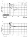
- FIGS. 7A and 7B are simulation waveform diagrams of the variable equalizer circuit of FIG. It is a circuit diagram which shows the structure of the variable equalizer circuit which concerns on a 1st modification. It is a circuit diagram which shows the structure of the variable equalizer circuit which concerns on a 2nd modification. It is a circuit diagram which shows the structure of the variable equalizer circuit which concerns on a 4th modification.
- the state in which the member A is connected to the member B means that the member A and the member B are physically directly connected, or the member A and the member B are electrically connected. The case where it is indirectly connected through another member that does not affect the state is also included.
- the state in which the member C is provided between the member A and the member B refers to the case where the member A and the member C or the member B and the member C are directly connected, as well as an electrical condition. It includes the case of being indirectly connected through another member that does not affect the connection state.
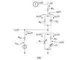
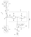
- FIG. 1 is a circuit diagram showing a configuration of a test apparatus 2 including a variable equalizer circuit 100 according to an embodiment.
- the test apparatus 2 is connected to the DUT 1 via the transmission line 3 and determines the quality of the DUT 1 based on a signal output from the DUT 1 or identifies a defective part.
- the DUT 1 includes a driver Dr and an output resistance Ru.
- the driver Dr1 applies a signal under test Vu to one end of the transmission line 3 via the output resistor Ru.
- the terminator 6 includes a termination driver Dr2 and a termination resistor Rd.
- the termination driver Dr2 applies a termination voltage Vd to the other end of the transmission line 3 via a termination resistor Rd.
- the terminator 6 may function as a transmission circuit (driver) that outputs a signal to the DUT 1.
- the receiving circuit 8 receives the signal under test Vu output from the DUT 1.
- the receiving circuit 8 is a comparator or a buffer.
- the test apparatus 2 determines the quality of the DUT 1 by comparing the signal under test received by the receiving circuit 8 with an expected value. Alternatively, the test apparatus 2 measures the amplitude margin and timing margin of the signal under test.
- the waveform of the signal under test output from the DUT 1 is distorted when passing through the transmission line 3 or a connector (not shown) (hereinafter referred to as a transmission line).
- the test apparatus 2 includes a variable equalizer circuit 100 provided in the preceding stage of the receiving circuit 8.
- variable equalizer circuit 100 equalizes the signal Va from the communication partner DUT 1 input to the input terminal P1, attenuates (annetates) the signal Va, and outputs the signal Va to the receiving circuit 8 via the output terminal P2.
- the variable equalizer circuit 100 includes an equalizing unit 10 and a level shifter 20.
- the equalizing unit 10 includes a first resistor R1, a second resistor R2, a first capacitor C1, a second capacitor C2, and at least one shunt resistor Rs.
- the first resistor R1 is a variable resistor whose resistance value is variable, and is provided between the output terminal P2 and a fixed voltage terminal (ground terminal).
- the first capacitor C1 is a variable capacitor having a variable capacitance value, and is provided in parallel with the first resistor R1 between the output terminal P2 and the ground terminal.
- the second resistor R2 is provided between the input terminal P1 and the output terminal P2.
- the second capacitor C2 is provided in parallel with the second resistor R2 between the input terminal P1 and the output terminal P2.
- At least one shunt resistor Rs is provided on a path including the first capacitor C1 and the second capacitor C2 from the input terminal P1 to the ground terminal.
- FIG. 1 shows a third resistor R3 and a fourth resistor Rc as the shunt resistor Rs.
- the third resistor R3 is provided between one end (N1) commonly connected to the second resistor R2 and the second capacitor C2 and the input terminal P1.
- the resistance value of the third resistor R3 is sufficiently larger than the characteristic impedance (50 ⁇ ) of the transmission line 3, and is desirably about 5 to 10 times the characteristic impedance, for example.
- the fourth resistor Rc is provided in series with the first capacitor C1 on a path parallel to the first resistor R1.
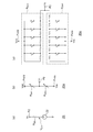
- FIGS. 2A to 2C are circuit diagrams showing configuration examples of variable resistors and variable capacitors.
- FIG. 2A shows a configuration example of the first resistor R1.
- the first resistor R1 includes a first terminal P11, a second terminal P12, a plurality of resistors R1 1 to R1 6 provided in series between the first terminal P11 and the second terminal P12, and a connection between adjacent resistors.
- a plurality of switches SW1 1 to SW1 5 are provided between the point (tap) and the second terminal P12. By switching the plurality of switches SW1 1 to SW1 5 on and off, the resistance value between the first terminal P11 and the second terminal P12 can be switched.
- the switches SW1 1 to SW1 5 are arranged on the fixed voltage terminal (ground terminal) side.
- the number of resistors R1 is arbitrary.
- FIG. 2B shows a configuration example of the first capacitor C1.
- the first capacitor C1 includes a plurality of capacitors C1 1 to C1 4 provided in parallel between the first terminal P21 and the second terminal P22.
- the plurality of switches SW2 1 to SW2 4 are provided in series with the plurality of capacitors C1 1 to C1 4 , respectively. By switching the states of the plurality of switches SW2 1 to SW2 4 , the capacitance value between the first terminal P21 and the second terminal P22 can be switched.
- the switches SW2 1 to SW2 4 are also desirably arranged on the fixed voltage terminal (ground terminal) side.
- the number of capacitors C1 1 to C1 4 is also arbitrary.
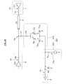
- FIG. 2C is a circuit diagram showing a configuration example of the switches SW1 and SW2 used in FIGS. 2A and 2B.
- the switch SW is a so-called transfer gate, and includes a first transistor M1 of an N-channel MOSFET and a second transistor M2 of a P-channel MOSFET that are provided in parallel between the first terminal P31 and the second terminal P32. .
- the control signal S1 is input to the gate of the first transistor M1, and the control signal # S1 inverted by the inverter 32 is input to the gate of the second transistor M2.
- conduction and interruption between the first terminal P31 and the second terminal P32 are switched.
- only the N-channel MOSFET or only the P-channel MOSFET may be used.
- variable resistors and the variable capacitors is not limited to those shown in FIGS. 2A to 2C, and their topology may be designed according to the required resistance value and capacitance value.
- the level shifter 20 shifts the voltage level of the output terminal P2.
- the receiving circuit 8 is a comparator or a differential amplifier
- the input voltage range is a limited range.
- the level shifter 20 by shifting the potential of the output terminal P2 by the level shifter 20 so as to match the input voltage range of a comparator or the like, high-speed or accurate operation can be expected.
- FIGS. 3A to 3C are circuit diagrams showing configuration examples of the level shifter 20.
- the level shifter 20 in FIG. 3A includes a voltage source 22 that generates the first voltage V SH and a fifth resistor R SH provided between the voltage source 22 and the output terminal P2.
- the level shifter 20, by switching the first voltage V SH, can modulate the level shift amount.
- FIG. 3B is a circuit diagram illustrating another configuration example of the level shifter.
- the level shifter 20a includes a first fixed voltage terminal (power supply terminal) Pvdd to which a first fixed voltage (power supply voltage vdd) is applied, and a second fixed voltage (ground voltage vss) different from the first fixed voltage (power supply voltage vdd). a second fixed voltage terminal (ground terminal) PVSS but applied, the first variable resistor R SH1 provided between the first fixed voltage terminal Pvdd and the output terminal P2, the second fixed voltage terminal PVSS and the output terminal P2 2nd variable resistance RSH2 provided between these.
- R1 // R2 is an operator representing the combined impedance of the resistors R1 and R2 connected in parallel.
- formula (A2) is obtained.
- R SH1 R SH ⁇ (vdd ⁇ vss) / (V SH ⁇ vss)
- R SH2 R SH ⁇ (vdd ⁇ vss) / (Vdd ⁇ V SH ) (A2)
- FIG. 3C is a circuit diagram showing a more specific configuration of the level shifter 20a of FIG.
- the variable resistors shown in FIG. 2A are used as the first variable resistor R SH1 and the second variable resistor R SH2 .
- the plurality of switches SW are preferably provided on the fixed voltage terminals Pvdd and Pvss sides.
- Each switch SW has a parasitic capacitance (not shown).
- the second resistor R2 and the second capacitor C2 act as a peaking filter for the signal Va input to the input terminal P1.
- Capacitance value C 2 of second capacitor C2 is determined such that the overcompensation.
- the first resistor R1 and the first capacitor C1 are variable resistors and variable capacitors, and function to adjust the characteristics of the entire variable equalizer circuit 100 by adjusting them. Specifically by the capacitance value C 1 of the first capacitor C1, it is possible to suppress the overcompensation provided by the second capacitor C2. Here, a relationship of C 2 > C 1 is established between the capacitance values of the first capacitor C1 and the second capacitor C2. Further, the boost amount of the equalizer can be controlled by the resistance value of the first resistor R1.
- the user of the test apparatus can measure or calculate the amount of distortion that the signal output from the DUT 1 receives by the transmission line 3 and the like and the frequency characteristics of the distortion prior to the test. Therefore, the user can determine the circuit constants of the first resistor R1 and the first capacitor C1 so as to cancel the distortion caused by the transmission line 3 and the like.
- the signal input to the input terminal P1 is equalized by the equalizing unit 10 and simultaneously attenuated.
- the level shifter 20 level-shifts the output signal of the equalizing unit 10 and outputs it to the receiving circuit 8.
- FIG. 4 is a circuit diagram showing a configuration of a variable equalizer circuit 300 according to the comparison technique.
- the variable equalizer circuit 300 includes an equalizing unit 310 and a level shifter 320.
- the equalizing unit 310 includes a third resistor R3, a second resistor R2 that is a variable resistor, and a second capacitor C2 that is a variable capacitor.
- variable equalizer circuit 300 of FIG. 4 when the second resistor R2 is configured with a variable resistor as shown in FIG. 2A, the parasitic capacitance CR2 of the switch is connected between the signal path and the ground terminal. Similarly, when the second capacitor C2 is configured with a variable capacitance as shown in FIG. 2B, the parasitic capacitance C2 of the switch is connected between the signal path and the ground terminal.
- These parasitic capacitances C R2 and C C2 act to smooth the signal input to the receiving circuit 8. That is, the original operation of the equalizer circuit is canceled out. This means that the response speed of the circuit is reduced.
- the second resistor R2 and the second capacitor C2 are constituted by fixed elements, and the first resistor R1 and the first capacitor C1 are constituted by variable elements.
- parasitic capacitance C C1 of the parasitic capacitance C R1 and first capacitor C1 of the first resistor R1 since the signal path from the input terminal P1 to the output terminal P2 are not directly connected, to improve the response speed of the circuit it can.
- variable equalizer circuit 100 has the following advantages.
- variable equalizer circuit 100 can change the boost amount and the time constant by adjusting the first capacitor C1 and the first resistor R1.
- variable equalizer circuit 100 Since the variable equalizer circuit 100 includes a resistor, a capacitor, and a transistor, the variable equalizer circuit 100 has a configuration suitable for integration on a semiconductor chip. In addition, since the inductor is not included, there is an advantage that the circuit area can be reduced and the oscillatory behavior is not caused.
- variable equalizer circuit 100 attenuates simultaneously with equalizing, the voltage level input to the receiving circuit 8 can be lowered. Therefore, since the receiving circuit 8 can be configured using high-speed and low-breakdown-voltage transistors, it is possible to receive high-speed signals.
- the influence of the variable equalizer circuit 100 on the impedance matching between the terminator 6 and the DUT 1 can be reduced. Furthermore, the band can be improved by providing the fourth resistor Rc.
- variable equalizer circuit 100 is analyzed qualitatively.
- the output resistance Ru of the DUT 1, the termination resistance Rd of the terminator 6, and the characteristic impedance Zo of the transmission line 3 are impedance matched.
- the impedance of the node N2 is Zo / 2.
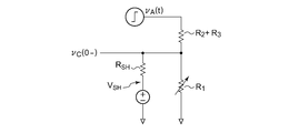
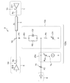
- FIG. 5 is a simplified circuit diagram of the variable equalizer circuit 100 of FIG.
- R 1 is the resistance value of the first resistor R 1
- R 2 is the resistance value of the second resistor R 2
- R 3 is the resistance value of the third resistor R 3
- R c is the resistance value of the fourth resistor Rc
- C 1 the capacitance of the first capacitor C1
- C 2 represents the capacitance value of the second capacitor C2.
- Equation (1) is obtained from Kirchhoff's current law.
- Equation (7) is obtained.
- Equation (7) ′ is obtained.
- V P (s) is eliminated from equation (7) ′ and I C1 (s) is solved, equation (8) is obtained.
- Equation (1) Substituting Equations (2) ′ to (6) ′ and Equation (8) into Equation (1) ′ yields Equation (9).
- Expression (10) is obtained from the left side and the middle side of Expression (9).
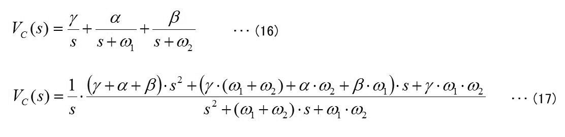
- Equation (16) can be fractionally decomposed as in equation (16), ⁇ , ⁇ , ⁇ , ⁇ 1 and ⁇ 2 are obtained. If ⁇ , ⁇ , ⁇ , ⁇ 1 , and ⁇ 2 are all real numbers, Equation (16) can be subjected to inverse Laplace transform, and a response v C (t) on the time axis can be obtained.
- the reason for partial fractional decomposition as in equation (16) is based on the fact that the response of this circuit is not oscillatory because the variable equalizer circuit 100 of FIG. 1 is composed of resistors and capacitors. By dividing equation (16), equation (17) is obtained.
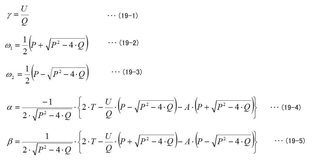
- equations (18-1) to (18-5) are solved, equations (19-1) to (19-5) are obtained.
- Expression (16) is obtained by inverse Laplace transform of Expression (16).
- Expression (20) is defined only in the range of 0 ⁇ t. At t ⁇ 0, the circuit is considered to be in a static state and v C (0 ⁇ ) is calculated.
- FIG. 6 is an equivalent circuit diagram of the variable equalizer circuit in a static state. In the static state, the capacitor can be considered open. 6 and 5, the same voltage and current state should be obtained when 0 ⁇ t. Therefore, when v C (0 ⁇ ) is calculated from the circuit model of FIG. 6, Equation (21) is obtained.
- FIG. 7A and 7B are simulation waveform diagrams of the variable equalizer circuit 100 of FIG. Figure 7 (a) shows a resistance value R 1 of the first resistor R1 2k ⁇ , 4k ⁇ , 6k ⁇ , 8k ⁇ , the waveform when changing the 10 k.OMEGA.
- Other circuit constants are as follows.
- R 2 1.75 k ⁇
- R 3 250 ⁇
- C 2 300 fF
- FIG. 8 is a circuit diagram showing a configuration of a variable equalizer circuit 100a according to the first modification.
- FIG. 9 is a circuit diagram showing a configuration of a variable equalizer circuit 100b according to a second modification.
- the third resistor R3 is omitted from the variable equalizer circuit 100 of FIG.
- the resistance values of the second resistor R2, the first resistor R1, and the fourth resistor Rc are sufficiently larger than the characteristic impedance Zo of the transmission line 3, the variable equalizer circuit 100 does not affect the impedance matching. R3 can be omitted.
- FIG. 10 is a circuit diagram showing a configuration of a variable equalizer circuit 100c according to a fourth modification.
- the variable equalizer circuit 100c of FIG. 10 has a configuration in which the first resistor R1 is omitted from the variable equalizer circuit 100 of FIG. 1, and the resistor R SH of the level shifter 20c is made variable instead.
- a resistance component R SH between the output terminal P2 and a fixed voltage terminal is variably configured.
- the first modification can be combined with the second and third modifications.
- the second modification can be combined with the first, third, and fourth modifications.
- the third modification can be combined with the first, second, and fourth modifications.
- the fourth modification can be combined with the second and third modifications. It is understood by those skilled in the art that various combinations and modifications exist within a range not impairing the effects of the present invention.
- variable equalizer circuit 100 In the embodiment, the case where the variable equalizer circuit 100 is used for the test apparatus 2 has been described. However, the use of the variable equalizer circuit 100 is not limited thereto, and the variable equalizer circuit can be used for various devices that receive signals from the outside. Can be used.
- the present invention can be used for telecommunications.
Landscapes
- Engineering & Computer Science (AREA)
- Physics & Mathematics (AREA)
- General Physics & Mathematics (AREA)
- General Engineering & Computer Science (AREA)
- Computer Networks & Wireless Communication (AREA)
- Signal Processing (AREA)
- Microelectronics & Electronic Packaging (AREA)
- Computer Hardware Design (AREA)
- Dc Digital Transmission (AREA)
- Networks Using Active Elements (AREA)
- Tests Of Electronic Circuits (AREA)
- Filters And Equalizers (AREA)
- Cable Transmission Systems, Equalization Of Radio And Reduction Of Echo (AREA)
Abstract
Description
この態様によれば、被試験デバイスから出力された信号を、伝送線路等に起因する歪みを補正した上で試験することができる。
可変イコライザ回路100は、入力端子P1に入力された通信相手のDUT1からの信号Vaをイコライジングし、同時に減衰(アネテーション)して出力端子P2を介して受信回路8に出力する。
イコライジング部10は、第1抵抗R1、第2抵抗R2、第1キャパシタC1、第2キャパシタC2、少なくともひとつのシャント抵抗Rsを備える。
なお、第1端子P31と第2端子P32の電圧の関係によっては、NチャンネルMOSFETのみとしてもよいし、PチャンネルMOSFETのみとしてもよい。
RSH=RSH1//RSH2
VSH=(vdd・RSH2+vss・RSH1)/(RSH1+RSH2) …(A1)
ここで「R1//R2」は、並列接続された抵抗R1、R2の合成インピーダンスを表す演算子である。
式(A1)を、RSH1、RSH2について解くと、式(A2)を得る。
RSH1=RSH・(vdd-vss)/(VSH-vss)
RSH2=RSH・(vdd-vss)/(Vdd-VSH) …(A2)
R1は、第1抵抗R1の抵抗値を、R2は第2抵抗R2の抵抗値を、R3は第3抵抗R3の抵抗値を、Rcは第4抵抗Rcの抵抗値を、C1は第1キャパシタC1の容量値を、C2は第2キャパシタC2の容量値を示す。


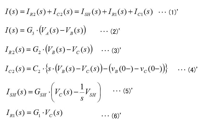


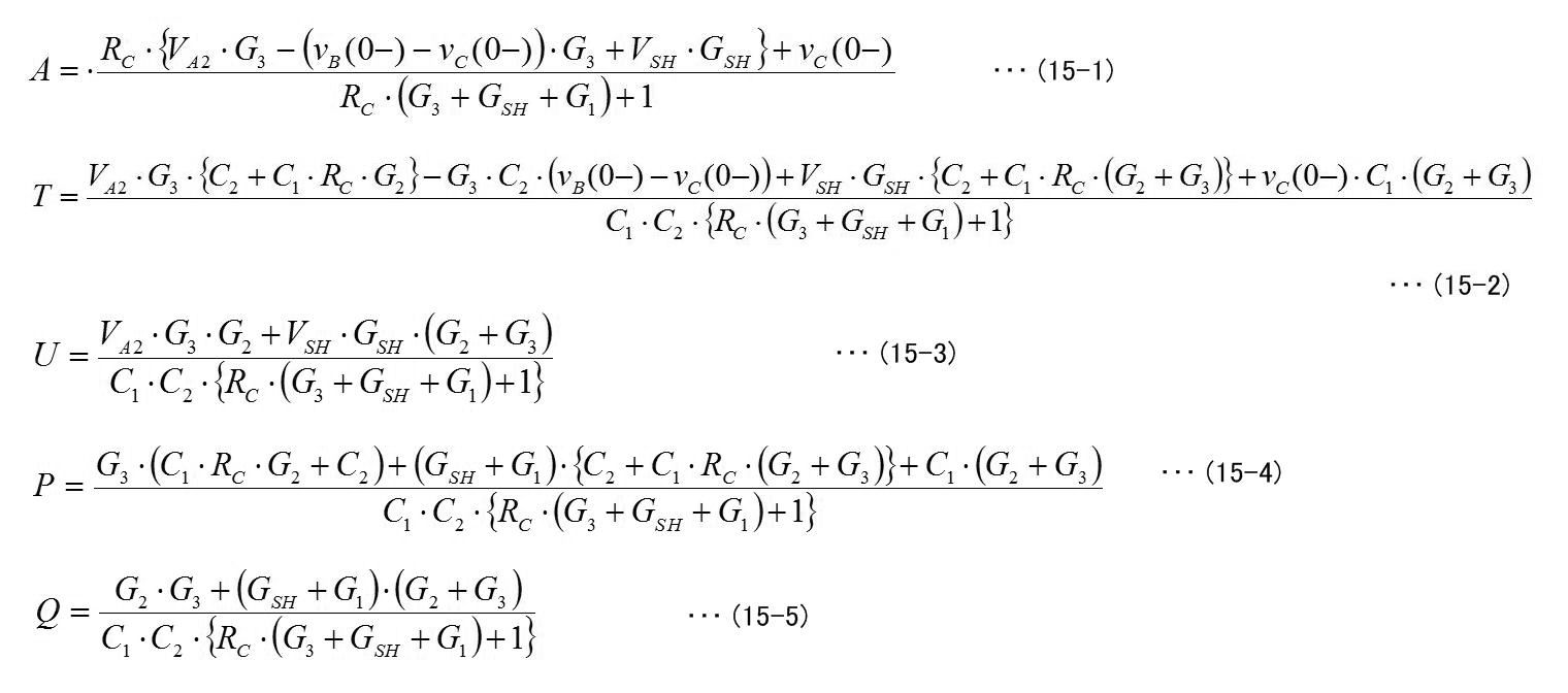



vA(t)が式(11)に示したステップ関数であれば、t=∞においても回路は静的であるため、図6を用いて、式(22)のようにvC(∞)を計算できる。また減衰率ATTは、式(23)で与えられる。
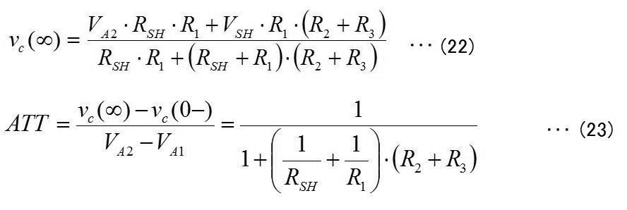
図7(a)は、第1抵抗R1の抵抗値R1を2kΩ、4kΩ、6kΩ、8kΩ、10kΩと変化させたときの波形を示す。その他の回路定数は以下の通りである。
R2=1.75kΩ
R3=250Ω
RC=2kΩ
C1=60fF
C2=300fF
第1抵抗R1の抵抗値R1を変化させることにより、主としてブースト量が制御できることが確認される。
図8は、第1の変形例に係る可変イコライザ回路100aの構成を示す回路図である。図8の可変イコライザ回路100aは、図1の可変イコライザ回路100からレベルシフタ20を省略した構成である。この場合でも、式(2)~(23)は、RSH=∞とすればそのまま成り立つ。レベルシフトしなくても、可変イコライザ回路100aの出力信号が受信回路8の入力電圧範囲に含まれる場合には、レベルシフタ20を省略することができる。
図9は、第2の変形例に係る可変イコライザ回路100bの構成を示す回路図である。図9の可変イコライザ回路100bは、図1の可変イコライザ回路100から第4抵抗Rcを省略した構成となっている。この場合、式(2)~(23)は、Rc=0とすればそのまま成り立つ。
第3の変形例は、図1の可変イコライザ回路100から第3抵抗R3を省略した構成である。第2抵抗R2、第1抵抗R1、第4抵抗Rcの抵抗値が伝送線路3の特性インピーダンスZoに比べて十分に大きい場合、可変イコライザ回路100はインピーダンス整合に影響を及ぼさないため、第3抵抗R3を省略することができる。
図10は、第4の変形例に係る可変イコライザ回路100cの構成を示す回路図である。図10の可変イコライザ回路100cは、図1の可変イコライザ回路100から第1抵抗R1を省略し、その代わりにレベルシフタ20cの抵抗RSHを可変とした構成を有する。レベルシフタ20cは、出力端子P2と固定電圧端子(接地端子もしくは電源端子)間の抵抗成分RSHが可変に構成される。この場合、式(2)~(23)は、R1=∞とすればそのまま成り立つ。
たとえば第1の変形例は、第2、第3の変形例と組み合わせることが可能である。
たとえば第2の変形例は、第1、第3、第4の変形例と組み合わせることが可能である。
たとえば第3の変形例は、第1、第2、第4の変形例と組み合わせることが可能である。
たとえば第4の変形例は、第2、第3の変形例と組み合わせることが可能である。
当業者には、本発明の効果を損なわない範囲において、さまざまな組み合わせ、変形例が存在することが理解される。
Claims (11)
- 通信相手のデバイスから伝送線路を介して受けた信号をイコライジングする可変イコライザ回路であって、
前記伝送線路と接続される入力端子と、
出力端子と、
前記出力端子と固定電圧端子の間に設けられ、その抵抗値が可変に構成される第1抵抗と、
前記出力端子と前記固定電圧端子の間に、前記第1抵抗と並列に設けられ、その容量値が可変に構成される第1キャパシタと、
前記入力端子と前記出力端子の間に設けられた第2抵抗と、
前記入力端子と前記出力端子の間に前記第2抵抗と並列に設けられた第2キャパシタと、
前記入力端子から前記固定電圧端子に至る前記第1キャパシタおよび前記第2キャパシタを含む経路上に設けられたシャント抵抗と、
を備えることを特徴とする可変イコライザ回路。 - 前記シャント抵抗は、
前記第2抵抗および前記第2キャパシタの共通に接続された一端と前記入力端子の間に設けられた第3抵抗を含むことを特徴とする請求項1に記載の可変イコライザ回路。 - 前記シャント抵抗は、
前記第1抵抗と並列な経路上に、前記第1キャパシタと直列に設けられた第4抵抗を含むことを特徴とする請求項1または2に記載の可変イコライザ回路。 - 前記出力端子の電圧レベルをシフトするレベルシフタをさらに備えることを特徴とする請求項1から3のいずれかに記載の可変イコライザ回路。
- 前記レベルシフタは、
第1電圧を発生する電圧源と、
前記電圧源と前記出力端子の間に設けられた第5抵抗と、
を含むことを特徴とする請求項4に記載の可変イコライザ回路。 - 前記レベルシフタは、
第1固定電圧が印加される第1固定電圧端子と、
前記第1固定電圧と異なる第2固定電圧が印加される第2固定電圧端子と、
前記第1固定電圧端子と前記出力端子の間に設けられた第1可変抵抗と、
前記第2固定電圧端子と前記出力端子の間に設けられた第2可変抵抗と、
を含むことを特徴とする請求項4に記載の可変イコライザ回路。 - 通信相手のデバイスから伝送線路を介して受けた信号をイコライジングする可変イコライザ回路であって、
前記伝送線路と接続される入力端子と、
出力端子と、
前記出力端子と固定電圧端子の間に設けられ、その容量値が可変に構成される第1キャパシタと、
前記入力端子と前記出力端子の間に設けられた第2抵抗と、
前記入力端子と前記出力端子の間に前記第2抵抗と並列に設けられた第2キャパシタと、
前記入力端子から前記固定電圧端子に至る前記第1キャパシタおよび前記第2キャパシタを含む経路上に設けられたシャント抵抗と、
前記出力端子の電圧レベルをシフトするレベルシフタであって、前記出力端子と固定電圧端子間の抵抗成分が可変に構成されるレベルシフタと、
を備えることを特徴とする可変イコライザ回路。 - 前記シャント抵抗は、
前記出力端子と前記固定電圧端子の間に、前記第1キャパシタと直列に設けられた第4抵抗を含むことを特徴とする請求項7に記載の可変イコライザ回路。 - 前記シャント抵抗は、
前記第2抵抗および前記第2キャパシタの共通に接続された一端と前記入力端子の間に設けられた第3抵抗を含むことを特徴とする請求項7または8に記載の可変イコライザ回路。 - 前記レベルシフタは、
第1固定電圧が印加される第1固定電圧端子と、
前記第1固定電圧と異なる第2固定電圧が印加される第2固定電圧端子と、
前記第1固定電圧端子と前記出力端子の間に設けられた第1可変抵抗と、
前記第2固定電圧端子と前記出力端子の間に設けられた第2可変抵抗と、
を含むことを特徴とする請求項7から9のいずれかに記載の可変イコライザ回路。 - 被試験デバイスから伝送線路を介して信号を受信し、前記被試験デバイスを検査する試験装置であって、
前記被試験デバイスからの信号をイコライジングする請求項1から10のいずれかに記載の可変イコライザ回路と、
前記可変イコライザ回路の出力信号を受ける受信回路と、
を備えることを特徴とする試験装置。
Priority Applications (5)
| Application Number | Priority Date | Filing Date | Title |
|---|---|---|---|
| KR1020117020889A KR101239487B1 (ko) | 2010-03-31 | 2010-03-31 | 가변 이퀄라이저 회로 및 이를 이용한 시험 장치 |
| PCT/JP2010/002357 WO2011121658A1 (ja) | 2010-03-31 | 2010-03-31 | 可変イコライザ回路およびそれを用いた試験装置 |
| US13/266,330 US20120043968A1 (en) | 2010-03-31 | 2010-03-31 | Variable equalizer circuit |
| JP2011510597A JPWO2011121658A1 (ja) | 2010-03-31 | 2010-03-31 | 可変イコライザ回路およびそれを用いた試験装置 |
| TW100111278A TW201206100A (en) | 2010-03-31 | 2011-03-31 | Variable equalizer circuit and testing apparatus using the same |
Applications Claiming Priority (1)
| Application Number | Priority Date | Filing Date | Title |
|---|---|---|---|
| PCT/JP2010/002357 WO2011121658A1 (ja) | 2010-03-31 | 2010-03-31 | 可変イコライザ回路およびそれを用いた試験装置 |
Publications (1)
| Publication Number | Publication Date |
|---|---|
| WO2011121658A1 true WO2011121658A1 (ja) | 2011-10-06 |
Family
ID=44711456
Family Applications (1)
| Application Number | Title | Priority Date | Filing Date |
|---|---|---|---|
| PCT/JP2010/002357 Ceased WO2011121658A1 (ja) | 2010-03-31 | 2010-03-31 | 可変イコライザ回路およびそれを用いた試験装置 |
Country Status (5)
| Country | Link |
|---|---|
| US (1) | US20120043968A1 (ja) |
| JP (1) | JPWO2011121658A1 (ja) |
| KR (1) | KR101239487B1 (ja) |
| TW (1) | TW201206100A (ja) |
| WO (1) | WO2011121658A1 (ja) |
Cited By (2)
| Publication number | Priority date | Publication date | Assignee | Title |
|---|---|---|---|---|
| US20150304135A1 (en) * | 2012-12-06 | 2015-10-22 | Cortina Systems, Inc. | System and method for ac coupling |
| JP2022524715A (ja) * | 2019-01-31 | 2022-05-10 | テクトロニクス・インコーポレイテッド | 高速入出力マージン試験のためのシステム、方法及び装置 |
Families Citing this family (6)
| Publication number | Priority date | Publication date | Assignee | Title |
|---|---|---|---|---|
| KR101483018B1 (ko) * | 2013-11-20 | 2015-01-19 | 스마트파이 주식회사 | 고속 인터페이스 시스템에서의 장치 및 고속 인터페이스 시스템 |
| US10187031B2 (en) * | 2016-05-10 | 2019-01-22 | Qualcomm Incorporated | Tunable matching network |
| US10050624B2 (en) * | 2016-05-18 | 2018-08-14 | Cavium, Inc. | Process-compensated level-up shifter circuit |
| US11616529B2 (en) * | 2021-02-12 | 2023-03-28 | Macom Technology Solutions Holdings, Inc. | Adaptive cable equalizer |
| US12483449B2 (en) * | 2023-01-31 | 2025-11-25 | Nxp Usa, Inc. | Passive equalizer |
| WO2025228532A1 (en) | 2024-05-02 | 2025-11-06 | Advantest Corporation | Device for equalising attenuation of a signal by a transmission line and system for testing electronic devices |
Citations (3)
| Publication number | Priority date | Publication date | Assignee | Title |
|---|---|---|---|---|
| JPS5412242A (en) * | 1977-06-28 | 1979-01-29 | Nec Home Electronics Ltd | Cable equalizer circuit |
| JPH06331657A (ja) * | 1993-05-19 | 1994-12-02 | Yokogawa Electric Corp | プローブ |
| JP2003168947A (ja) * | 2001-12-03 | 2003-06-13 | Iwatsu Electric Co Ltd | アッテネーター回路 |
Family Cites Families (12)
| Publication number | Priority date | Publication date | Assignee | Title |
|---|---|---|---|---|
| JPH0856179A (ja) * | 1994-08-12 | 1996-02-27 | Miharu Tsushin Kk | Catv用増幅器の電圧制御型可変等化器 |
| JP3576702B2 (ja) * | 1996-06-12 | 2004-10-13 | 富士通株式会社 | 可変ハイパスフィルタ |
| TW480832B (en) * | 1999-12-20 | 2002-03-21 | Koninkl Philips Electronics Nv | An arrangement for receiving a digital signal from a transmission medium |
| WO2003044550A1 (fr) * | 2001-11-20 | 2003-05-30 | Advantest Corporation | Testeur de semi-conducteur |
| US20040061569A1 (en) * | 2002-09-27 | 2004-04-01 | Naom Chaplik | ADSL customer premises subscriber loop equalizer |
| US6937054B2 (en) * | 2003-05-30 | 2005-08-30 | International Business Machines Corporation | Programmable peaking receiver and method |
| JP4261432B2 (ja) * | 2004-07-09 | 2009-04-30 | 株式会社アドバンテスト | 半導体試験装置および半導体試験方法 |
| JP4310280B2 (ja) * | 2005-01-07 | 2009-08-05 | 株式会社アドバンテスト | インピーダンス変換回路、入出力回路及び半導体試験装置 |
| US20080186407A1 (en) * | 2007-02-01 | 2008-08-07 | Magenta Research | Signal Equalizer for Balanced Transmission Line-Based Video Switching |
| US7504906B2 (en) * | 2007-08-02 | 2009-03-17 | Inventec Corporation | Method for manufacturing an equalizer |
| US7924113B2 (en) * | 2008-02-15 | 2011-04-12 | Realtek Semiconductor Corp. | Integrated front-end passive equalizer and method thereof |
| US8698540B2 (en) * | 2008-04-03 | 2014-04-15 | Cognipower, Llc | DC common mode level shifter |
-
2010
- 2010-03-31 US US13/266,330 patent/US20120043968A1/en not_active Abandoned
- 2010-03-31 WO PCT/JP2010/002357 patent/WO2011121658A1/ja not_active Ceased
- 2010-03-31 KR KR1020117020889A patent/KR101239487B1/ko not_active Expired - Fee Related
- 2010-03-31 JP JP2011510597A patent/JPWO2011121658A1/ja not_active Withdrawn
-
2011
- 2011-03-31 TW TW100111278A patent/TW201206100A/zh unknown
Patent Citations (3)
| Publication number | Priority date | Publication date | Assignee | Title |
|---|---|---|---|---|
| JPS5412242A (en) * | 1977-06-28 | 1979-01-29 | Nec Home Electronics Ltd | Cable equalizer circuit |
| JPH06331657A (ja) * | 1993-05-19 | 1994-12-02 | Yokogawa Electric Corp | プローブ |
| JP2003168947A (ja) * | 2001-12-03 | 2003-06-13 | Iwatsu Electric Co Ltd | アッテネーター回路 |
Cited By (4)
| Publication number | Priority date | Publication date | Assignee | Title |
|---|---|---|---|---|
| US20150304135A1 (en) * | 2012-12-06 | 2015-10-22 | Cortina Systems, Inc. | System and method for ac coupling |
| US9515854B2 (en) * | 2012-12-06 | 2016-12-06 | Cortina Systems, Inc. | System and method for AC coupling |
| JP2022524715A (ja) * | 2019-01-31 | 2022-05-10 | テクトロニクス・インコーポレイテッド | 高速入出力マージン試験のためのシステム、方法及び装置 |
| JP7728174B2 (ja) | 2019-01-31 | 2025-08-22 | テクトロニクス・インコーポレイテッド | 試験装置、電気的マージン試験方法及びマージン・テスタ |
Also Published As
| Publication number | Publication date |
|---|---|
| TW201206100A (en) | 2012-02-01 |
| KR101239487B1 (ko) | 2013-03-07 |
| KR20120023598A (ko) | 2012-03-13 |
| US20120043968A1 (en) | 2012-02-23 |
| JPWO2011121658A1 (ja) | 2013-07-04 |
Similar Documents
| Publication | Publication Date | Title |
|---|---|---|
| WO2011121658A1 (ja) | 可変イコライザ回路およびそれを用いた試験装置 | |
| US10447427B2 (en) | Baseline wander correction | |
| JP5165877B2 (ja) | 電子回路及び制御方法 | |
| US9473330B1 (en) | Continuous time linear equalizer with a programmable negative feedback amplification loop | |
| TWI523439B (zh) | 用於通訊頻道上的補償模式轉換之系統與方法 | |
| JP4384207B2 (ja) | 半導体集積回路 | |
| US20100109739A1 (en) | Active guarding for reduction of resistive and capacitive signal loading with adjustable control of compensation level | |
| US11005688B2 (en) | Common-mode control for AC-coupled receivers | |
| CA2848033A1 (en) | Method and system for determining and improving performance of a cable | |
| KR20210148386A (ko) | 전압 드라이버 회로 | |
| US9941958B2 (en) | On-chip test interface for voltage-mode Mach-Zehnder modulator driver | |
| JP4944936B2 (ja) | 差動ハイブリッド回路およびそれを用いた試験装置 | |
| WO2010140190A1 (ja) | 比較判定回路およびそれを用いた試験装置 | |
| JP4848004B2 (ja) | 双方向データ伝送を行う通信回路 | |
| WO2010122603A1 (ja) | ドライバ・コンパレータ回路およびそれを用いた試験装置 | |
| US7501863B2 (en) | Voltage margining with a low power, high speed, input offset cancelling equalizer | |
| US20080049872A1 (en) | Method and device for matching output impedance of a transmitter | |
| JP4977056B2 (ja) | 試験装置 | |
| US11394376B2 (en) | Crosstalk cancellation circuit, transmitter, and transmission and reception system | |
| JP4874210B2 (ja) | 試験装置 | |
| TWI836478B (zh) | 衰減器電路、電子裝置及相關方法 | |
| TWI749401B (zh) | 回音消除電路 | |
| Lee | Application of active inductors in high-speed I/O circuits | |
| Sewter | Electronic equalization of polarization-mode dispersion in 40-GB/S optical systems | |
| Faust | Analog and mixed-signal circuitry for system-assisted high-speed I/O links |
Legal Events
| Date | Code | Title | Description |
|---|---|---|---|
| WWE | Wipo information: entry into national phase |
Ref document number: 2011510597 Country of ref document: JP |
|
| ENP | Entry into the national phase |
Ref document number: 20117020889 Country of ref document: KR Kind code of ref document: A |
|
| WWE | Wipo information: entry into national phase |
Ref document number: 13266330 Country of ref document: US |
|
| 121 | Ep: the epo has been informed by wipo that ep was designated in this application |
Ref document number: 10848841 Country of ref document: EP Kind code of ref document: A1 |
|
| NENP | Non-entry into the national phase |
Ref country code: DE |
|
| 122 | Ep: pct application non-entry in european phase |
Ref document number: 10848841 Country of ref document: EP Kind code of ref document: A1 |