WO2011111585A1 - 無線電力伝送用磁気素子及び電力供給装置 - Google Patents
無線電力伝送用磁気素子及び電力供給装置 Download PDFInfo
- Publication number
- WO2011111585A1 WO2011111585A1 PCT/JP2011/054770 JP2011054770W WO2011111585A1 WO 2011111585 A1 WO2011111585 A1 WO 2011111585A1 JP 2011054770 W JP2011054770 W JP 2011054770W WO 2011111585 A1 WO2011111585 A1 WO 2011111585A1
- Authority
- WO
- WIPO (PCT)
- Prior art keywords
- magnetic
- power transmission
- wireless power
- conductor
- magnetic element
- Prior art date
Links
Images


Classifications
-
- H—ELECTRICITY
- H01—ELECTRIC ELEMENTS
- H01F—MAGNETS; INDUCTANCES; TRANSFORMERS; SELECTION OF MATERIALS FOR THEIR MAGNETIC PROPERTIES
- H01F38/00—Adaptations of transformers or inductances for specific applications or functions
- H01F38/14—Inductive couplings
-
- H—ELECTRICITY
- H02—GENERATION; CONVERSION OR DISTRIBUTION OF ELECTRIC POWER
- H02J—CIRCUIT ARRANGEMENTS OR SYSTEMS FOR SUPPLYING OR DISTRIBUTING ELECTRIC POWER; SYSTEMS FOR STORING ELECTRIC ENERGY
- H02J50/00—Circuit arrangements or systems for wireless supply or distribution of electric power
- H02J50/005—Mechanical details of housing or structure aiming to accommodate the power transfer means, e.g. mechanical integration of coils, antennas or transducers into emitting or receiving devices
-
- H—ELECTRICITY
- H02—GENERATION; CONVERSION OR DISTRIBUTION OF ELECTRIC POWER
- H02J—CIRCUIT ARRANGEMENTS OR SYSTEMS FOR SUPPLYING OR DISTRIBUTING ELECTRIC POWER; SYSTEMS FOR STORING ELECTRIC ENERGY
- H02J50/00—Circuit arrangements or systems for wireless supply or distribution of electric power
- H02J50/70—Circuit arrangements or systems for wireless supply or distribution of electric power involving the reduction of electric, magnetic or electromagnetic leakage fields
-
- H—ELECTRICITY
- H02—GENERATION; CONVERSION OR DISTRIBUTION OF ELECTRIC POWER
- H02J—CIRCUIT ARRANGEMENTS OR SYSTEMS FOR SUPPLYING OR DISTRIBUTING ELECTRIC POWER; SYSTEMS FOR STORING ELECTRIC ENERGY
- H02J50/00—Circuit arrangements or systems for wireless supply or distribution of electric power
- H02J50/10—Circuit arrangements or systems for wireless supply or distribution of electric power using inductive coupling
-
- H—ELECTRICITY
- H02—GENERATION; CONVERSION OR DISTRIBUTION OF ELECTRIC POWER
- H02J—CIRCUIT ARRANGEMENTS OR SYSTEMS FOR SUPPLYING OR DISTRIBUTING ELECTRIC POWER; SYSTEMS FOR STORING ELECTRIC ENERGY
- H02J50/00—Circuit arrangements or systems for wireless supply or distribution of electric power
- H02J50/40—Circuit arrangements or systems for wireless supply or distribution of electric power using two or more transmitting or receiving devices
- H02J50/402—Circuit arrangements or systems for wireless supply or distribution of electric power using two or more transmitting or receiving devices the two or more transmitting or the two or more receiving devices being integrated in the same unit, e.g. power mats with several coils or antennas with several sub-antennas
Definitions
- the present invention relates to a magnetic element for wireless power transmission and a power supply device that transmit power in a non-contact manner by electromagnetic induction.
- Patent Document 1 by embedding a spiral-type planar coil on one surface of a magnetic layer, disposing a magnetic window at the center of the planar coil, and configuring at least a part of the magnetic window with a magnetic material, Proposals have been made that can realize high transmission efficiency and miniaturization.
- the present invention has been made in view of the above problems, and an object of the present invention is to provide a magnetic element and a power supply device for wireless power transmission that can supply power with high transmission efficiency.
- the present invention is a magnetic element for wireless power transmission that induces an induced electromotive force by magnetic coupling,
- a magnetic element for wireless power transmission that induces an induced electromotive force by magnetic coupling
- a cross section that matches the magnetic coupling direction a plurality of conductor portions in which an alternating current flows in the same direction, and a magnetic body portion provided in one or more gaps between the conductor portions, the magnetic coupling direction They are arranged in parallel in the orthogonal direction, and either one of the conductor portion and the magnetic body portion has a protruding region protruding in the magnetic coupling direction than the other.
- the magnetic field generated by the flow of alternating current to the conductor part generates an induced current by interlacing with another conductor part, and this induced current acts as a resistance to the conductor in the protruding region. It can suppress by the magnetic body part provided in the clearance gap between parts. As a result, due to the high magnetic flux density and the reduction of the resistance due to the induced current, it is possible to supply and receive power with high transmission efficiency when used on either the magnetic coupling side or the magnetic coupling side.
- protruding regions in the present invention may be disposed on both sides in the magnetic coupling direction.
- positioned at the other side of the magnetic coupling direction can exhibit the same function as the magnetic body provided in the arrangement direction of the conductor part arrange
- the protruding region in the present invention may be arranged in the whole arrangement direction of the conductor portions.
- the protruding region is present in the entire arrangement direction of the conductor portions, it is possible to supply and receive power with higher transmission efficiency.
- the magnetic part in the present invention may be made of a soft magnetic material.
- the soft magnetic material may be a metallic magnetic material.
- the metallic magnetic material may be an amorphous magnetic material.
- the magnetic element for wireless power transmission includes a long conductor portion, a long magnetic body portion arranged in parallel along the longitudinal direction of the conductor portion, the conductor portion, and the magnetic member.
- One of the body portions has a protruding region in which one end in the width direction protrudes from the other end in the width direction.
- the magnetic field generated by the flow of alternating current to the conductor part generates an induced current by interlacing with another conductor part, and the phenomenon in which this induced current acts as a resistance is observed along the conductor part. Can be suppressed by the magnetic body portions arranged in parallel. As a result, due to the high magnetic flux density and the reduction of the resistance due to the induced current, it is possible to supply and receive power with high transmission efficiency when used on either the magnetic coupling side or the magnetic coupling side.
- the conductor portion and the magnetic body portion may be joined so that at least a part thereof is integrated in an electrically insulated state.
- the conductor portion and the magnetic body portion are integrated by bonding, so that even when the conductor portion and the magnetic body portion receive external force such as vibration or impact, the conductor portion and Since the positional relationship of the magnetic part and the form of the protruding region can be maintained in the initial state, the initial high transmission efficiency can be maintained over a long period of time. Also, when the conductor part generates heat, the heat of the conductor part is efficiently transferred to the magnetic body part through the part where the conductor part is integrally joined. Can do. Thereby, the electric energy which supplies with electricity can be increased rather than the case where the conductor part and the magnetic body part are separated.
- the transmission amount can be increased while preventing overheating of the conductor portion with a simple configuration in which at least a part of the conductor portion and the magnetic body portion are integrated. Furthermore, since the handling is facilitated by the integration of the conductor portion and the magnetic body portion, the assembling work and storage in various devices are facilitated.
- the conductor portion has a coating made of an electrical insulator, and the magnetic body portion is joined to the coating so as to be integrated with the conductor portion. May be. That is, the conductor part may have a coating made of an electrical insulator, and the magnetic part may be bonded to the coating.
- a magnetic part having excellent thermal conductivity can be easily obtained, and the conductor part and the magnetic part can be easily integrated.
- the power supply apparatus of the present invention has a plurality of the above-described wireless power transmission magnetic elements, and these wireless power transmission magnetic elements are arranged on the same plane.
- the magnetic element 1 for wireless power transmission is configured to cause an induced electromotive force by magnetic coupling, and can be used for both power feeding and power receiving.
- the power supply apparatus 10 having a transmission power of about 0.1 W to 500 W and a transmission distance of 1 mm to 10 cm can be exemplified.
- the magnetic element 1 for wireless power transmission is embedded in a body, a power supply device 10 used for a wall-mounted device such as a wall-mounted thin TV, a power supply device 10 used for a mounting device such as a personal computer or a mouse.
- the magnetic element 1 for wireless power transmission can also be applied to the power supply device 10 that exceeds the above transmission power and transmission distance, for example, a power supply device 10 such as a robot or an electric vehicle.
- wall-mounted devices such as flat-screen TVs that are placed on or contacted with the power supply device 10 described above, mounted devices such as personal computers and mice, and small medical devices such as pacemakers embedded in the body.
- the wireless power transmission magnetic element 1 can be applied to a robot, an electric vehicle, or the like.
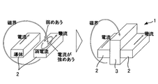
- the conductor portion 2 and the magnetic body portion 3 adjacent to the conductor portion 2 are orthogonal to the magnetic coupling direction in a cross section coinciding with the magnetic coupling direction. Are arranged in parallel in the direction.
- the wireless power transmission magnetic element 1 has a protruding region 61 in which one of the conductor portion 2 and the magnetic body portion 3 protrudes in the magnetic coupling direction more than the other.
- the wireless power transmission magnetic element 1 includes a long conductor portion 2, a long magnetic body portion 3 arranged in parallel along the longitudinal direction of the conductor portion 2, the conductor portion 2, and One of the magnetic body portions 3 has a protruding region 61 in which one end in the width direction protrudes from the other end in the width direction.
- the “magnetic coupling direction” is, for example, magnetically coupled to the magnetic coupling side (feeding side) as in the case where the central portions of the magnetic elements 1 for wireless power transmission having the same size are arranged to face each other.
- the side (power receiving side) is opposed to the strongest magnetically coupled to each other, the center portion of the side to be magnetically coupled and the side to be magnetically coupled in the positional relationship that generates the largest induced electromotive force It is a direction to connect.
- the “orthogonal direction” is almost perpendicular.
- the wireless power transmission magnetic element 1 configured as described above has a protrusion in which one of the conductor portion 2 and the magnetic body portion 3 protrudes in the magnetic coupling direction more than the other.
- the magnetic field ineffective for magnetic coupling around the conductor portion 2 is reduced and the spread of the entire magnetic field is suppressed as compared with the case where such a protruding region 61 is not provided. Is possible.
- the magnetic flux density at the time of magnetic coupling can be increased.
- even when the magnetic element 1 for wireless power transmission is used on either the magnetic coupling side or the magnetic coupling side, it is possible to supply and receive power with high transmission efficiency due to high magnetic flux density.
- the wireless power transmission magnetic element 1 has a configuration in which a plurality of conductor portions 2 are arranged in parallel in a cross section that coincides with the magnetic coupling direction, and a plurality of conductor portions 2 in which an alternating current flows in the same direction.
- the magnetic part 3 is provided in one or more gaps.
- the magnetic body portions 3 are provided in all the gaps between the conductor portions 2 and the conductor portions 2 and the magnetic body portions 3 are alternately arranged.
- a configuration in which an alternating current flows through the plurality of conductor portions 2 in the same direction is such that the long conductor portion 2 and the magnetic body portion 3 are wound from the inner peripheral side to the outer peripheral side.
- annular form from which the radius which matched the center point differs is illustrated.
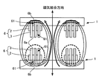
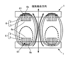
- the magnetic element 1 for wireless power transmission has a conductor assembly 6 as shown in FIG.
- the conductor assembly portion 6 has a flat outer shape, and has a front surface 6a and a back surface 6b that can be a magnetic open surface facing a power receiving side or power supply side device.
- the conductor assembly 6 can be formed with an arbitrary surface shape.
- the conductor assembly portion 6 may have a polygonal surface shape such as a triangle or a quadrangle in top view, or may have an elliptical or circular surface shape.
- the conductor assembly portion 6 includes a long conductor portion 2 and a long magnetic body portion 3.
- the conductor portion 2 and the magnetic body portion 3 are formed in a spiral shape with a gap at a constant interval from the inner peripheral side to the outer peripheral side.
- the conductor assembly portion 6 has a plurality of conductor portions 2 and a plurality of magnetic body portions 3 in a longitudinal section (AA 'line arrow cross section / BB' line arrow cross section) coinciding with the magnetic coupling direction. Are alternately arranged in parallel in a direction perpendicular to the magnetic coupling direction.
- a core portion made of a magnetic material may be disposed on the inner peripheral side of the conductor assembly portion 6.
- the magnetic field can be concentrated on the inner peripheral side of the conductor assembly 6.
- the magnetic element 1 for wireless power transmission may have a form in which the conductor assembly 6 is exposed to the outside, but in order to protect the surface, an insulating resin such as an epoxy resin or a polyimide resin, or a non-magnetic material such as glass.
- a coating film of a protective material made of an electrical insulator may be provided on the front surface 6 a and the back surface 6 b of the conductor assembly portion 6.
- the magnetic part 3 is made of a material having a high magnetic permeability. That is, the magnetic body portion 3 may be made of a soft magnetic material.
- the soft magnetic material may be a metal-based magnetic material.
- the metallic magnetic material may be an amorphous magnetic material.
- the magnetic body portion 3 is formed using a magnetic powder such as ferrite, sendust, amorphous (amorphous), or a magnetic material having fine crystals, which is solidified with a resin, or a rapid solidification method. It is formed by using a magnetic film formed by vapor deposition such as sputtering or vapor deposition or plating on a thin ribbon obtained by the above method or an insulating film.
- Examples of amorphous include Co-based amorphous and Fe-based amorphous, and examples of magnetic materials having fine crystals include Fe-based magnetic materials having fine crystals of 300 angstroms (0.03 ⁇ m) or less.
- Examples of the magnetic film formed by vapor deposition or plating include soft magnetic films such as CoZrNb, CoZrNbTa, FeBN, CoFeB—SiO, CoFeAlO, CoAlPdO, CoFeMn, CoFeN, and FeNi.
- the magnetic body portion 3 has a width that matches the magnetic coupling direction and a thickness that matches the direction orthogonal to the magnetic coupling direction (radial direction of the conductor assembly portion 6).
- the conductor portion 2 has one end portion and the other end portion in the longitudinal direction connected to a pair of terminals (not shown). Each terminal is connected to the power supply device 8 when the magnetic element 1 for wireless power transmission is applied to a power supply device such as the power supply device 10.
- the power supply device 8 can supply AC power to the conductor portion 2 at an arbitrary frequency.
- each terminal is connected to a rectifier.
- the rectifier is used for smoothing AC power formed by electromagnetic induction into DC power to charge a battery, or for operating a drive device.
- the conductor portion 2 is preferably formed of a metal material such as Cu or Al.
- the conductor portion 2 can be formed by vapor phase growth, plating, or etching.
- the conductor portion 2 has a width that matches the magnetic coupling direction and a thickness that matches the direction orthogonal to the magnetic coupling direction (radial direction of the conductor assembly portion 6).
- the magnetic body portion 3 when the magnetic body portion 3 is obtained by solidifying a powder of a magnetic material such as ferrite or amorphous with a resin, that is, when the magnetic body portion 3 has an insulating property, the magnetic body portion 3 and the conductor portion. 2 may be arranged in contact.
- an insulating layer needs to be disposed between the magnetic body portion 3 and the conductor portion 2. Examples of the insulating layer include an insulating resin such as polyethylene terephthalate and an inorganic insulating material such as an oxide.
- the wireless power transmission magnetic element 1 has a protruding region 61 in which one of the width direction end of the magnetic body portion 3 and the width direction end of the conductor portion 2 protrudes from the other.
- the protruding region 61 is set on the entire surface 6 a of the conductor assembly 6.
- region 61 may be set to either one of the surface 6a and the back surface 6b of the conductor assembly part 6, and may be set to a part of surface 6a and the back surface 6b.
- the protruding region 61 may be set to at least a part of at least one of the front surface 6 a and the back surface 6 b of the conductor assembly portion 6.
- the end of the magnetic body portion 3 in the width direction protrudes beyond the end of the conductor portion 2 in the width direction, so that the surface of the magnetic body portion 3 and the side surface of the protruding magnetic body portion 3 are external. It is preferable to be exposed. That is, it is preferable that the exposed area of the magnetic body portion 3 is increased in the protruding region 61.
- the magnetic body portion 3 being a material having a high magnetic permeability, it is easily affected by a magnetic field due to a large exposed area, and as shown in FIG. It is possible to prevent a decrease in the generation efficiency of the magnetic field due to the generation of the induced current due to the magnetic field intermingling between the two.
- the end portion in the width direction of the conductor portion 2 may protrude beyond the end portion in the width direction of the magnetic body portion 3. Even in this case, the magnetic body portion 3 between the adjacent conductor portions 2 and 2 can prevent a decrease in magnetic field generation efficiency due to generation of an induced current in each conductor portion 2 and 2.
- the protrusion length of the magnetic body part 3 or the conductor part 2 is preferably such that Dm / d is 0.2 to 3.0, where Dm is the width of the magnetic body part 3 and d is the width of the conductor part 2. If the protrusion length is too small, it will be difficult to exert the effect of preventing the reduction of the magnetic field generation efficiency. If the protrusion length is excessive, mechanical problems such as contact between the protrusions will occur. It is.
- the wireless power transmission magnetic element 1 configured as described above is applied for power feeding.
- the wireless power transmission magnetic element 1 is provided in a power supply apparatus 10 as shown in FIG.
- the power supply device 10 is formed in a sheet shape so that one or more devices 9 that operate by cordless power supply such as a mobile phone or a personal computer can be placed thereon.
- a large number of magnetic elements 1 for wireless power transmission are arranged on the entire surface of the power supply device 10.
- the wireless power transmission magnetic element 1 is formed by an etching process or a printing process in which a liquid material is jetted.
- the magnetic element 1 for wireless power transmission is preferably arranged in a plane with a uniform distribution density as in a matrix arrangement.
- electric power can be supplied with high transmission efficiency evenly in the entire power supply apparatus 10.
- the power supply device 10 may include a plurality of placement areas in which the distribution density of the wireless power transmission magnetic element 1 is changed.
- the power supply amount can be adjusted depending on the place where the device 9 is placed. For example, if the device 9 is a light-emitting device capable of dimming, the amount of light emission can be adjusted by changing the placement location.
- the magnetic element 1 for wireless power transmission is set so that the surface 6a serving as a magnetic emission surface (magnetic open surface) is aligned with the upper surface (mounting surface) of the power supply device 10.
- the magnetic open surface means a surface on the power feeding side or the power receiving side, and is at least one of the front surface 6a and the back surface 6b of the magnetic element 1 for wireless power transmission.
- the power supply apparatus 10 includes a placement layer 101 that directly contacts the device 9 and fixes and holds the conductor portion 2 and the magnetic body portion 3, a support layer 103 on which the wireless power transmission magnetic element 1 is formed, A shielding layer 104 provided on the lower surface of the support layer 103 and a protective layer 105 provided on the lower surface of the shielding layer 104 are provided.
- the mounting layer 101, the support layer 103, and the protective layer 105 are formed of a nonmagnetic synthetic resin or the like.
- the shielding layer 104 is formed of at least one of a conductive material and a magnetic material, and prevents leakage of a magnetic field from the lower side (back side) of the power supply device 10.
- the support layer 103 is provided with a sheet-like power circuit board (not shown). The power supply circuit board enables high-frequency AC power from the power supply device 8 to be supplied to each wireless power transmission magnetic element 1.
- each wireless power transmission magnet Element 1 when the power supply device 8 is connected to the power supply device 10 in which the magnetic element 1 for wireless power transmission is incorporated and a high-frequency alternating current (alternating current power) is supplied, each wireless power transmission magnet Element 1 generates an alternating magnetic field.
- each wireless power transmission magnetic element 1 is magnetic in one or more gaps between a plurality of conductor portions 2 in which an alternating current flows in the same direction in a cross section that coincides with the magnetic coupling direction.
- the body part 3 is provided, and one of the conductor part 2 and the magnetic body part 3 has a protruding region 61 that protrudes in the magnetic coupling direction from the other. Therefore, as shown in FIG.
- each wireless power transmission magnetic element 1 reduces the magnetic field ineffective for magnetic coupling around the conductor portion 2 as compared with the case where the protruding region 61 is not provided. It is possible to suppress the spread of the magnetic field. As a result, each magnetic element for wireless power transmission 1 can increase the magnetic flux density toward the device 9 placed on the power supply device 10. Thereby, the power supply device 10 including a large number of magnetic elements 1 for wireless power transmission can supply power to the device 9 with high transmission efficiency.
- each of the wireless power transmission magnetic elements 1 the magnetic field generated by the flow of the alternating current to the conductor portion 2 is interlaced with other adjacent conductor portions 2. By doing so, an induced current is generated.
- the phenomenon in which the induced current acts as a resistance is suppressed by the magnetic body portion 3 provided in the gap between the conductor portions 2 and 2 in the protruding region 61. Accordingly, power can be supplied with high transmission efficiency due to the high magnetic flux density and the reduction in resistance due to the induced current.
- the power supply device 10 including these wireless power transmission magnetic elements 1 is supplied with AC power.
- An alternating magnetic field having a frequency corresponding to the frequency is output over the entire surface. Therefore, when the device 9 that operates using the induced electromotive force is placed on the power supply device 10, as shown in FIG. 2, the coil built in the device 9 is magnetically coupled to the alternating magnetic field. Inductive electromotive force is generated. Then, the AC power is rectified and supplied to the control chip or the like.
- the device 9 may include the wireless power transmission magnetic element 1 for power reception. In this case, power supply and power reception can be performed with higher efficiency.
- the wireless power transmission magnetic element 1 of the present embodiment has been described with respect to the configuration in which the protruding region 61 is disposed on the surface 6a of the conductor assembly 6 as shown in FIGS.
- the present invention is not limited to this. That is, as shown in FIG. 5, the magnetic element 1 for wireless power transmission may have the protruding regions 61 disposed on the front surface 6a and the back surface 6b. In this case, as shown in FIG. 6, the wireless power transmission magnetic element 1 can increase the magnetic flux density in the magnetic coupling direction.
- the protruding region 61 may be disposed only on the back surface 6b opposite to the magnetic open surface. Even in this case, as shown in FIG. 8, the wireless power transmission magnetic element 1 can increase the magnetic flux density in the magnetic coupling direction.
- the protruding region 61 may be disposed only on the inner peripheral side of the conductor assembly portion 6. In the magnetic element 1 for wireless power transmission, the protruding region 61 may be arranged only on the outer peripheral side of the conductor assembly 6.
- the magnetic element 1 for wireless power transmission has a protruding region 61 whose protruding length is reduced from the inner peripheral side to the outer peripheral side so that the protruding area of the magnetic body portion 3 on the inner peripheral side of the conductor assembly 6 is maximized. You may do it.
- a plurality of magnetic body portions 3, 3 may be disposed with a gap between the conductor portions 2, 2, or a plurality of conductor portions 2 may be disposed with a gap between the magnetic body portions 3, 3. It may be.
- the wireless power transmission magnetic element 1 may be a combination of the above configurations.
- the magnetic element for wireless power transmission 201 includes a conductor layer 202 through which an alternating current flows and a magnetic layer 203 arranged in parallel to the longitudinal direction of the conductor layer 202.
- the laminated body 204 is provided with the wound body 206, and the end portion in the width direction of the magnetic layer 203 has a protruding region 261 that protrudes from the end portion in the width direction of the conductor layer 202. Note that the protruding region 261 only needs to protrude either from the width direction end of the magnetic layer 203 or the width direction end of the conductor layer 202 from the other.
- the wireless power transmission magnetic element 201 has a wound body 206.
- the wound body 206 has a cylindrical outer shape, and has a side peripheral surface 206a and end surfaces 206b and 206b that are disposed at both ends of the side peripheral surface 206a and can be magnetic open surfaces.
- the wound body 206 can be formed in an arbitrary outer shape, and may be, for example, a polygonal prism shape having an end face 206b such as a triangle or a quadrangle.
- the wound body 206 is formed by winding the strip-shaped laminated body 204 a plurality of times. As a result, the wound body 206 has a configuration in which a plurality of stacked bodies 204 are arranged in parallel to each other in the radial direction in the longitudinal section in the axial direction (cross section taken along line A-A ′).
- the laminate 204 is wound around the outer peripheral surface of a cylindrical core member 207.
- the core member 207 may be a non-magnetic material or a magnetic material, but is a magnetic material in that the magnetic field can be concentrated on the inner peripheral side of the wound body 206 on which the core member 207 is disposed. Preferably there is.
- the laminated body 204 may be wound in a hollow shape without the core member 207.
- the winding shape may be any winding shape such as a circle, an ellipse, and a rectangle.
- the laminate 204 includes a conductor layer 202 and a magnetic layer 203.
- the conductor layer 202 and the magnetic layer 203 are arranged in parallel to each other.
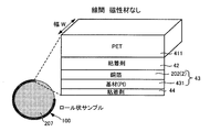
- the laminate 204 includes a magnetic sheet 41 having a magnetic layer 203 interposed between protective sheets 411 and 412 of polyethylene terephthalate (PET), polyimide (PI).
- PET polyethylene terephthalate
- PI polyimide
- a conductor sheet 43 having a conductor layer 202 formed on a base material 431 made of polyimide).
- the wireless power transmission magnetic element 201 may have a form in which the wound body 206 is exposed to the outside, but in order to protect the surface, an insulating resin such as an epoxy resin or a polyimide resin, or a non-magnetic material such as glass.
- an insulating resin such as an epoxy resin or a polyimide resin
- a non-magnetic material such as glass.
- a coating film of a protective material made of an electrical insulator may be provided on the side peripheral surface 206a and the end surface 206b of the wound body 206.
- the magnetic element 201 for wireless power transmission may be filled with a protective material between the magnetic layers 203 and 203 in order to prevent contact and deformation between the magnetic layers 203 and 203 adjacent in the radial direction. .
- the magnetic layer 203 is made of the same material as that of the magnetic part 3 in the first embodiment.
- the magnetic layer 203 is formed in a strip shape having a width perpendicular to the longitudinal direction that is the winding direction (circumferential direction) of the wound body 206 and a thickness that matches the radial direction of the wound body 206.
- the thickness of the magnetic layer 203 is preferably 100 ⁇ m or less. In terms of magnetic properties, there is no problem even if it exceeds 100 ⁇ m, but considering the winding, the thickness of the magnetic layer is preferably 100 ⁇ m or less, and more preferably 50 ⁇ m or less.
- the lower limit value of the thickness of the magnetic layer 203 is preferably 0.1 ⁇ m or more.
- the thickness is less than 0.1 ⁇ m, the magnetic layer is thin and sufficient magnetic properties may not be obtained. Moreover, it is preferable that the thickness of the thin magnetic layer is 0.1 ⁇ m or more because manufacturing management becomes complicated. Considering the thickness of such a magnetic layer, an amorphous material capable of obtaining a ribbon (ribbon) by a rapid solidification method is a preferable material. In particular, if it is Co-based amorphous, the magnetic properties are also good.
- the conductor layer 202 is formed of the same material as that of the conductor portion 2 in the first embodiment.
- the conductor layer 202 is preferably formed of a metal material such as Cu or Al.
- the shape of the conductor layer 202 may be a thin film (ribbon shape) or a thin film such as vapor phase growth or plating.
- the wireless power transmission magnetic element 201 has a protruding region 261.
- the protruding region 261 is set on all of both end faces 206 b and 206 b of the wound body 206.
- region 261 may be set to either one end surface 206b * 206b of the wound body 206, and may be set to a part of end surface 206b.
- the protruding region 261 may be set to at least a part of at least one of the end surfaces 206b and 206b of the wound body 206.
- the wireless power transmission magnetic element 201 configured as described above is provided in a power supply apparatus 210 as shown in FIG.
- the power supply device 210 is formed in a sheet shape or a flat plate shape so that one or more devices 9 that operate by cordless power supply such as a mobile phone or a personal computer can be placed.
- Numerous wireless power transmission magnetic elements 201 are embedded in the entire surface of the power supply apparatus 210.
- the wireless power transmission magnetic element 201 is set such that one end face 206b serving as a magnetic emission surface (magnetic open surface) is an upper surface.
- the power supply device 210 includes a mounting layer 101 that is in direct contact with the device 9, a holding layer 102 that fixes and holds the side peripheral surface 206 a of the wireless power transmission magnetic element 201, and a wireless power transmission magnetic element 201.
- the support layer 103 that supports the end surface 206 b serving as the lower surface, the shielding layer 104 provided on the lower surface of the support layer 103, and the protective layer 105 provided on the lower surface of the magnetic layer 104 are provided.
- the mounting layer 101, the holding layer 102, the support layer 103, and the protective layer 105 are formed of a nonmagnetic synthetic resin or the like.
- the shielding layer 104 is formed of at least one of a conductive material and a magnetic material, and prevents leakage of a magnetic field from the lower side of the power supply device 210. Further, between the shielding layer 104 and the support layer 103, a sheet-like circuit board (not shown) connected to the inner peripheral side and the outer peripheral side of the conductor layer 202 in each wireless power transmission magnetic element 201 is provided. Yes. The circuit board enables high-frequency AC power from the power supply device 8 to be supplied to each wireless power transmission magnetic element 201.
- the magnetic element 1 (201) for wireless power transmission in the first embodiment (second embodiment) described above at least a part of the conductor portion 2 (conductor layer 202) and the magnetic body portion 3 (magnetic body layer 203) is included. You may join so that it may integrate in an electrically insulated state.
- the electrically insulated state can be realized by interposing an insulator between the conductor portion 2 (conductor layer 202) and the magnetic body portion 3 (magnetic body layer 203).
- a method of interposing an insulator a method in which a film made of an insulating material is deposited or plated on at least one of the conductor 2 (conductor layer 202) and the magnetic body 3 (magnetic layer 203) is joined.
- a method of sandwiching an insulating sheet between the conductor 2 (conductor layer 202) and the magnetic body 3 (magnetic layer 203) can be mentioned.
- the insulator and the magnetic part 3 (magnetic layer 203) have higher thermal conductivity than that of the air layer.
- the conductor part 2 (conductor layer 202) and a magnetic body are obtained by integrating at least one part of the conductor part 2 (conductor layer 202) and the magnetic body part 3 (magnetic body layer 203). Even when the portion 3 (magnetic material layer 203) receives external force such as vibration or impact, the positional relationship between the conductor portion 2 (conductor layer 202) and the magnetic material portion 3 (magnetic material layer 203) or the protruding region 61 (261) Thus, the initial high transmission efficiency can be maintained over a long period of time.
- the conductor 2 (conductor layer 202) generates heat
- the heat of the conductor 2 (conductor layer 202) is efficiently applied to the magnetic body 3 (magnetic layer 203) via the part where the heat is integrally joined. Therefore, the heat of the conductor 2 (conductor layer 202) can be efficiently radiated in the magnetic body 3 (magnetic layer 203).
- the electric energy to supply can be increased.
- the magnetic element 1 (201) for wireless power transmission in the above-described first embodiment (second embodiment) has a film in which the conductor portion 2 (conductor layer 202) is made of an electrical insulator, and the magnetic portion 3 ( The magnetic layer 203) may be bonded to the coating so as to be integrated with the conductor 2 (conductor layer 202). That is, the conductor portion 2 (conductor layer 202) may have a coating made of an electrical insulator, and the magnetic body portion 3 (magnetic layer 203) may be bonded to this coating.
- the magnetic element 1 (201) for wireless power transmission is obtained easily. be able to. Moreover, an effect equivalent to the roll coil which is the wound shape in the above-described embodiment can be obtained.
- the transmission state of the wireless power transmission magnetic element 201 having the protruding region 261 is measured as Examples 1 to 3, and the transmission state of the wireless power transmission magnetic element not having the protruding region 261 is measured as Comparative Examples 1 and 2. did.
- Example 1 Specifically, as shown in FIG. 10, an 18 ⁇ m magnetic layer 203 made of an amorphous magnetic alloy mainly composed of iron is interposed between protective sheets 411 and 412 made of 50 ⁇ m polyethylene terephthalate. A magnetic sheet 41 was prepared. Moreover, the conductor sheet 43 in which the conductor layer 202 made of a 35 ⁇ m copper foil was formed on a 25 ⁇ m polyimide substrate 431 was prepared.
- the magnetic sheet 41 was cut into a width of 7 mm and a length of 300 mm. Further, the conductor sheet 43 was cut into a width of 5 mm and a length of 300 mm. The magnetic sheet 41 and the conductor sheet 43 were laminated so that one end in the width direction was aligned and the other end of the magnetic sheet 41 protruded from the conductor sheet 43 by 2 mm. And both sheets 41 * 43 were joined by the adhesive layer of 20 micrometers, and it was set as the laminated body 204.
- a wound body 206 having a protruding region 261 on one side was formed.
- One end of the signal line was connected to the inner peripheral end and the outer peripheral end of the conductor layer 202 in the wound body 206, respectively.
- wound bodies 206 and 206 are prepared, and the wound bodies 206 and 206 are placed on the left and right so that the 2 mm portions of the magnetic sheets 41 and 41 in these wound bodies 206 and 206 face each other. Arranged symmetrically. That is, the wound bodies 206 and 206 are arranged so that the protruding regions 261 face each other. At this time, the distance at which the conductor layers 202 face each other was 5 mm. In addition, the wound bodies 206 and 206 were held so that the axis of the wound bodies 206 and 206 were concentric.
- S-parameter insertion loss S21 was measured.
- S21 represents a signal that passes through the terminal 2 when a signal is input from the terminal 1, and is displayed in decibels. The larger the numerical value, the higher the transmission efficiency.
- Example 2 Prepare the two wound bodies 206 and 206 that are the same as in the first embodiment, and make the wound bodies 206 and 206 symmetrically so that the portions of the wound bodies 206 and 206 that are aligned at one end face each other. Arranged. That is, the wound bodies 206 and 206 are arranged so that the protruding regions 261 do not face each other. At this time, the distance at which the conductor layers 202 face each other was 5 mm. And the insertion loss (S21) of S parameter was measured on the same conditions as Example 1 with the measurement frequency of 300 kHz, 500 kHz, and 1000 kHz.
- Example 3 Next, the same magnetic sheet 41 as in Example 1 was cut into a width of 9 mm and a length of 300 mm. Further, the same conductor sheet 43 as in Example 1 was cut into a width of 5 mm and a length of 300 mm. And the laminated body 204 was formed by aligning the center of the magnetic sheet 41 and the conductor sheet 43, and laminating
- Two wound bodies 206 and 206 were prepared, and the wound bodies 206 and 206 were arranged symmetrically so that one ends of these wound bodies 206 and 206 face each other. At this time, the distance at which the conductor layers 202 face each other was 5 mm. And the insertion loss (S21) of S parameter was measured on the same conditions as Example 1 with the measurement frequency of 300 kHz, 500 kHz, and 1000 kHz.
- the magnetic element 100 for wireless power transmission without the protruding region 261 was created. That is, the same magnetic sheet 41 and conductor sheet 43 as in Example 1 were cut into a width of 5 mm and a length of 300 mm. And the laminated body 204 was formed by laminating
- the laminated body 204 was wound around a winding core member 207 made of cork having a diameter of 13 mm.phi.
- the wound bodies 206 and 206 were arranged symmetrically so that one ends of the two wound bodies 206 and 206 face each other. At this time, the distance at which the conductor layers 202 face each other was 5 mm. And the insertion loss (S21) of S parameter was measured on the same conditions as Example 1 with the measurement frequency of 300 kHz, 500 kHz, and 1000 kHz.
- the magnetic element 100 for wireless power transmission without the magnetic layer 203 was produced. That is, instead of the magnetic sheet 41 of Example 1, a laminate 204 using the protective sheet 411 having the same thickness was formed.
- the laminated body 204 was wound around a winding core member 207 made of cork having a diameter of 13 mm.phi.
- the wound bodies 206 and 206 were arranged symmetrically so that one ends of the two wound bodies 206 and 206 face each other. At this time, the interval between the wound bodies 206 and 206 was set to a distance of 5 mm.
- the insertion loss (S21) of S parameter was measured on the same conditions as Example 1 with the measurement frequency of 300 kHz, 500 kHz, and 1000 kHz.
- the transmission efficiency is higher in Examples 1 to 3 in which the protruding regions 261 exist than in Comparative Example 1 in which the protruding regions 261 do not exist and Comparative Example 2 in which the magnetic layer 203 does not exist. It has been found. From this, it has been clarified that the wireless power transmission magnetic element 201 is provided with the protruding region 261 in which the magnetic layer 203 protrudes in the width direction rather than the conductor layer 202, thereby increasing the transmission efficiency.
- the transmission efficiency of the third embodiment including the wound body 206 having the protruding regions 261 on both sides is higher than that of the first and second embodiments including the wound body 206 having the protruding regions 261 on only one side. It has been found. Furthermore, it has been found that the transmission efficiency is higher in Example 2 in which the protruding regions 261 are not opposed to each other than in Example 1 in which the protruding regions 261 are opposed. As a result, it is important to increase the transmission efficiency that the protruding regions 261 exist on both sides including the magnetic open surface, and the transmission efficiency is improved even if the protruding regions 261 are not arranged on the magnetic open surface side. Became clear.
Landscapes
- Engineering & Computer Science (AREA)
- Power Engineering (AREA)
- Computer Networks & Wireless Communication (AREA)
- Physics & Mathematics (AREA)
- Electromagnetism (AREA)
- Charge And Discharge Circuits For Batteries Or The Like (AREA)
- Soft Magnetic Materials (AREA)
- Near-Field Transmission Systems (AREA)
- Coils Or Transformers For Communication (AREA)
Abstract
Description
前記磁気結合方向に一致する断面において、交流電流が同一方向に流通する複数の導体部と、これら導体部間の1以上の隙間に設けられた磁性体部とが、前記磁気結合方向に対して直交方向に並列配置されており、前記導体部及び前記磁性体部の何れか一方が他方よりも前記磁気結合方向に突出された突出領域を有する。
以下、本発明の好適な第1の実施形態について、図面を参照しつつ説明する。
(無線電力伝送用磁気素子1)
図1に示すように、無線電力伝送用磁気素子1は、磁気結合により誘導起電力を引き起こすように構成されており、給電用及び受電用の何れにも用いることができる。給電用としては、送電電力が0.1W~500W程度で送電距離が1mm~10cmの電力供給装置10を例示することができる。例えば、無線電力伝送用磁気素子1は、壁掛け用薄型テレビ等の壁掛け型の機器に用いられる電力供給装置10、パーソナルコンピュータやマウス等の載置型の機器に用いられる電力供給装置10、体内に埋め込まれるペースメーカ等の小型医療機器に用いられる電力供給装置10に適用可能である。尚、無線電力伝送用磁気素子1は、上記の送電電力及び送電距離を超えた電力供給装置10、例えば、ロボットや電気自動車等の電力供給装置10に適用することも可能である。
磁性体部3は、高透磁率の材料により形成されている。即ち、磁性体部3は、軟磁性材料により形成されていてもよい。軟磁性材料は、金属系磁性材料であってもよい。金属系磁性材料は、アモルファス磁性材であってもよい。具体的には、磁性体部3は、フェライト、センダスト、アモルファス(非晶質)、微細結晶を有する磁性材料等の磁性粉末を樹脂で固めたものを用いて形成されたり、或いは、急冷凝固法等によって得られた薄帯、絶縁フィルム上にスパッタや蒸着等の気相成長またはメッキにより成膜した磁性膜を用いて形成されている。また、アモルファスは、Co系アモルファス、Fe系アモルファスが挙げられ、微細結晶を有する磁性材料は、300オングストローム(0.03μm)以下の微細結晶を有するFe系磁性材料が挙げられる。また、気相成長またはメッキによる磁性膜としては、CoZrNb系、CoZrNbTa系、FeBN系、CoFeB-SiO系、CoFeAlO系、CoAlPdO系、CoFeMn系、CoFeN系、FeNi系等の軟磁性膜が挙げられる。
導体部2は、長手方向の一端部と他端部とが図示しない一対の端子にそれぞれ接続されている。各端子は、無線電力伝送用磁気素子1が電力供給装置10等の給電装置に適用される場合、電源装置8に接続される。電源装置8は、任意の周波数で交流電力を導体部2に供給可能にしている。一方、無線電力伝送用磁気素子1が受電装置に適用される場合には、各端子が整流装置に接続される。整流装置は、電磁誘導により形成された交流電力を直流電力に平滑化してバッテリを充電したり、駆動機器の作動に用いられる。
無線電力伝送用磁気素子1は、磁性体部3の幅方向端部と導体部2の幅方向端部との何れか一方が他方よりも突出された突出領域61を有している。突出領域61は、導体集合部6の表面6aの全部に設定されている。尚、突出領域61は、導体集合部6の表面6a及び裏面6bの何れか一方に設定されていてもよいし、表面6a及び裏面6bの一部に設定されていてもよい。換言すれば、突出領域61は、導体集合部6の表面6a及び裏面6bの少なくとも一方における少なくとも一部に設定されていればよい。
上記のように構成された無線電力伝送用磁気素子1が給電用に適用された場合を説明する。無線電力伝送用磁気素子1は、図1に示すように、電力供給装置10に備えられている。電力供給装置10は、携帯電話やパーソナルコンピュータ等のコードレスの給電により作動する1以上の機器9を載置可能にシート状に形成されている。電力供給装置10の全面には、多数の無線電力伝送用磁気素子1が配置されている。尚、無線電力伝送用磁気素子1は、エッチング処理や液状の材料を噴射する印刷処理により形成されている。
上記の構成において、無線電力伝送用磁気素子1が組み込まれた電力供給装置10に対して電源装置8が接続され、高周波の交流電流(交流電力)が供給されると、各無線電力伝送用磁気素子1が交番磁場を生成する。この際、図2に示すように、各無線電力伝送用磁気素子1は、磁気結合方向に一致する断面において、交流電流が同一方向に流通する複数の導体部2間の1以上の隙間に磁性体部3が設けられ、導体部2及び磁性体部3の何れか一方が他方よりも磁気結合方向に突出された突出領域61を有している。従って、図3に示すように、各無線電力伝送用磁気素子1は、突出領域61が設けられていない場合と比較して、導体部2周辺における磁気結合にとって無効な磁界を減少させると共に、全体的な磁界の広がりを抑制することが可能になる。この結果、各無線電力伝送用磁気素子1は、電力供給装置10に載置された機器9に向かう磁束密度を高めることが可能になる。これにより、多数の無線電力伝送用磁気素子1を備えた電力供給装置10は、機器9に対して高い伝送効率で電力を給電することができる。
以上のように、本実施形態の無線電力伝送用磁気素子1は、図1及び図3に示すように、突出領域61が導体集合部6の表面6aに配置された構成について説明しているが、これに限定されるものではない。即ち、無線電力伝送用磁気素子1は、図5に示すように、突出領域61が表面6aと裏面6bとに配置されていてもよい。この場合には、図6に示すように、無線電力伝送用磁気素子1は、磁気結合方向における磁束密度を高めることが可能になる。
以下、本発明の好適な第2の実施形態について、図面を参照しつつ説明する。尚、第1の実施形態と同一の部材には同一の符号を付記して、その説明を省略する。
図9に示すように、本実施形態に係る無線電力伝送用磁気素子201は、交流電流が流通する導体層202と、導体層202の長手方向に平行に配置された磁性体層203とを有した積層体204の巻回体206を備えていると共に、磁性体層203の幅方向端部が導体層202の幅方向端部よりも突出された突出領域261を有している。尚、突出領域261は、磁性体層203の幅方向端部及び導体層202の幅方向端部の何れか一方が他方よりも突出されていればよい。
磁性体層203は、第1の実施形態における磁性体部3と同様の材料により形成されている。磁性体層203は、巻回体206の巻方向(周方向)である長手方向に直交する幅と、巻回体206の半径方向に一致する厚みとを有した帯状に形成されている。磁性体層203の厚みは、100μm以下が好ましい。磁気特性と言う点では100μmを超えても問題はないが、巻回することを考慮すると磁性体層の厚みは100μm以下が好ましく、さらには50μm以下が好ましい。また、磁性体層203の厚みの下限値は、0.1μm以上が好ましい。0.1μm未満では、磁性層が薄く充分な磁気特性が得られない恐れがあるからである。また、薄い磁性層を均一に作製するのは製造上の管理が煩雑になることから0.1μm以上が好ましい。このような磁性層の厚みを考慮すると、急冷凝固法により薄帯(リボン)を得ることのできるアモルファスが好ましい材料となる。特にCo系アモルファスであれば磁気特性も良好である。
導体層202は、第1の実施形態における導体部2と同様の材料により形成されている。導体層202は、Cu、Al等の金属材料で形成されていることが好ましい。導体層202の形態は、薄帯状(リボン状)の他、気相成長やメッキ等の薄膜であってもよい。
無線電力伝送用磁気素子201は、突出領域261を有している。突出領域261は、巻回体206の両端面206b・206bの全部に設定されている。尚、突出領域261は、巻回体206の何れか一方の端面206b・206bに設定されていてもよいし、端面206bの一部に設定されていてもよい。換言すれば、突出領域261は、巻回体206の少なくとも一方の端面206b・206bの少なくとも一部に設定されていればよい。
上記のように構成された無線電力伝送用磁気素子201は、図9に示すように、電力供給装置210に備えられている。電力供給装置210は、携帯電話やパーソナルコンピュータ等のコードレスの給電により作動する1以上の機器9を載置可能にシート状や平板状に形成されている。電力供給装置210の全面には、多数の無線電力伝送用磁気素子201が埋め込まれている。無線電力伝送用磁気素子201は、磁気的な放出面(磁気開放面)となる一方の端面206bが上面となるように設定されている。
具体的には、図10に示すように、50μmのポリエチレンテレフタラートからなる保護シート411・412間に、鉄を主成分としたアモルファス磁性合金製からなる18μmの磁性体層203が介装された磁性シート41を準備した。また、25μmのポリイミド製の基材431に、35μmの銅箔からなる導体層202が形成された導体シート43を準備した。
実施例1と同一の2個の巻回体206・206を準備し、これらの巻回体206・206における一端を揃えた部分同士が向い合うように、巻回体206・206を左右対称に配置した。即ち、突出領域261同士が対向しないように巻回体206・206を配置した。この際、導体層202同士が対向する間隔は、5mmの距離とした。そして、実施例1と同一の条件で、300kHz、500kHz、及び1000kHzの測定周波数でSパラメータの挿入損失(S21)を測定した。
次に、実施例1と同一の磁性シート41を幅9mm×長さ300mmに切り出した。また、実施例1と同一の導体シート43を幅5mm×長さ300mmに切り出した。そして、磁性シート41と導体シート43との中心を揃え、磁性シート41の両端が銅箔から2mm出るように積層することにより積層体204を形成した。積層体204を径13mmφのコルクからなる巻芯部材207に、6.5回の巻回数で巻き付けることによって、両側に突出領域261が存在する巻回体206を形成した。
次に、突出領域261が存在しない無線電力伝送用磁気素子100を作成した。即ち、実施例1と同一の磁性シート41及び導体シート43を幅5mm×長さ300mmに切り出した。そして、磁性シート41と導体シート43との両端面が同一となるように積層することにより積層体204を形成した。積層体204を径13mmφのコルクからなる巻芯部材207に、6.5回の巻回数で巻き付けることにより巻回体206とした。2個の巻回体206・206における一端同士が向い合うように、巻回体206・206を左右対称に配置した。この際、導体層202同士が対向する間隔は、5mmの距離とした。そして、実施例1と同一の条件で、300kHz、500kHz、及び1000kHzの測定周波数でSパラメータの挿入損失(S21)を測定した。
次に、図11に示すように、磁性体層203が存在しない無線電力伝送用磁気素子100を作成した。即ち、実施例1の磁性シート41の代わりに、同一厚みの保護シート411を用いた積層体204を形成した。積層体204を径13mmφのコルクからなる巻芯部材207に、6.5回の巻回数で巻き付けることにより巻回体206とした。2個の巻回体206・206における一端同士が向い合うように、巻回体206・206を左右対称に配置した。この際、巻回体206・206の間隔は、5mmの距離とした。そして、実施例1と同一の条件で、300kHz、500kHz、及び1000kHzの測定周波数でSパラメータの挿入損失(S21)を測定した。
上記のようにしてSパラメータの挿入損失(S21)を測定した結果を表1に示すと共に図12に示す。

2 導体部
3 磁性体部
6 導体集合部
8 電源装置
9 機器
10 電力供給装置
61 突出領域
201 無線電力伝送用磁気素子
202 導体層
203 磁性体層
204 積層体
Claims (15)
- 磁気結合により誘導起電力を引き起こす無線電力伝送用磁気素子であって、
前記磁気結合方向に一致する断面において、交流電流が同一方向に流通する複数の導体部と、これら導体部間の1以上の隙間に設けられた磁性体部とが、前記磁気結合方向に対して直交方向に並列配置されており、
前記導体部及び前記磁性体部の何れか一方が他方よりも前記磁気結合方向に突出された突出領域を有することを特徴とする無線電力伝送用磁気素子。 - 前記突出領域は、前記磁気結合方向の両側に配置されていることを特徴とする請求項1に記載の無線電力伝送用磁気素子。
- 前記突出領域は、前記導体部の配列方向の全体に配置されていることを特徴とする請求項2に記載の無線電力伝送用磁気素子。
- 前記磁性体部は、軟磁性材料により形成されていることを特徴とする請求項3に記載の無線電力伝送用磁気素子。
- 前記軟磁性材料は、金属系磁性材料であることを特徴とする請求項4に記載の無線電力伝送用磁気素子。
- 前記金属系磁性材料は、アモルファス磁性材であることを特徴とする請求項5に記載の無線電力伝送用磁気素子。
- 前記導体部と前記磁性体部とは、少なくとも一部が電気的絶縁状態で一体化するように接合されていることを特徴とする請求項4に記載の無線電力伝送用磁気素子。
- 前記導体部が電気的絶縁体からなる被膜を有し、該皮膜に前記磁性体部が接合されていることを特徴とする請求項7に記載の無線電力伝送用磁気素子。
- 前記突出領域は、前記導体部の配列方向の全体に配置されていることを特徴とする請求項1に記載の無線電力伝送用磁気素子。
- 前記磁性体部は、アモルファス磁性材により形成されていることを特徴とする請求項1に記載の無線電力伝送用磁気素子。
- 前記導体部と前記磁性体部とは、電気的絶縁状態で一体化するように接合されていることを特徴とする請求項1に記載の無線電力伝送用磁気素子。
- 長尺状の導体部と、
前記導体部の長手方向に沿うように並列配置された長尺状の磁性体部と、
前記導体部及び前記磁性体部の何れか一方の幅方向端部が他方の幅方向端部よりも突出された突出領域とを有することを特徴とする無線電力伝送用磁気素子。 - 前記導体部と前記磁性体部とは、少なくとも一部が電気的絶縁状態で一体化するように接合されていることを特徴とする請求項12に記載の無線電力伝送用磁気素子。
- 前記導体部が電気的絶縁体からなる被膜を有し、該皮膜に前記磁性体部が接合されていることを特徴とする請求項13に記載の無線電力伝送用磁気素子。
- 請求項1乃至14の何れか1項に記載の無線電力伝送用磁気素子を複数有し、これら無線電力伝送用磁気素子を同一平面上に位置するように配置したことを特徴とする電力供給装置。
Priority Applications (5)
| Application Number | Priority Date | Filing Date | Title |
|---|---|---|---|
| DK11753244.0T DK2546843T3 (en) | 2010-03-09 | 2011-03-02 | Magnetic element for wireless power transfer and power supply arrangement |
| KR1020127026202A KR20130014546A (ko) | 2010-03-09 | 2011-03-02 | 무선 전력 전송용 자기 소자 및 전력 공급 장치 |
| US13/583,525 US9390849B2 (en) | 2010-03-09 | 2011-03-02 | Magnetic element for wireless power transmission and power supply device |
| CN201180013298.4A CN102792401B (zh) | 2010-03-09 | 2011-03-02 | 无线电力传输用磁元件和电力供给装置 |
| EP11753244.0A EP2546843B1 (en) | 2010-03-09 | 2011-03-02 | Magnetic element for wireless power transmission and power supply device |
Applications Claiming Priority (2)
| Application Number | Priority Date | Filing Date | Title |
|---|---|---|---|
| JP2010-052049 | 2010-03-09 | ||
| JP2010052049 | 2010-03-09 |
Publications (1)
| Publication Number | Publication Date |
|---|---|
| WO2011111585A1 true WO2011111585A1 (ja) | 2011-09-15 |
Family
ID=44563389
Family Applications (1)
| Application Number | Title | Priority Date | Filing Date |
|---|---|---|---|
| PCT/JP2011/054770 WO2011111585A1 (ja) | 2010-03-09 | 2011-03-02 | 無線電力伝送用磁気素子及び電力供給装置 |
Country Status (7)
| Country | Link |
|---|---|
| US (1) | US9390849B2 (ja) |
| EP (1) | EP2546843B1 (ja) |
| JP (1) | JP5364745B2 (ja) |
| KR (1) | KR20130014546A (ja) |
| CN (1) | CN102792401B (ja) |
| DK (1) | DK2546843T3 (ja) |
| WO (1) | WO2011111585A1 (ja) |
Cited By (4)
| Publication number | Priority date | Publication date | Assignee | Title |
|---|---|---|---|---|
| JP2013080785A (ja) * | 2011-10-03 | 2013-05-02 | Nissan Motor Co Ltd | 非接触給電装置 |
| JP2013243250A (ja) * | 2012-05-21 | 2013-12-05 | Kobe Steel Ltd | 非接触給電用コイル |
| EP2728968A1 (en) * | 2012-01-05 | 2014-05-07 | Nitto Denko Corporation | Wireless power supply-type light-emitting element, and light-emitting device |
| JP2015109061A (ja) * | 2013-10-23 | 2015-06-11 | 東芝テック株式会社 | チェックアウト端末 |
Families Citing this family (16)
| Publication number | Priority date | Publication date | Assignee | Title |
|---|---|---|---|---|
| JP2012204440A (ja) | 2011-03-24 | 2012-10-22 | Nitto Denko Corp | 無線電力伝送用磁気素子及びその製造方法 |
| WO2013019122A1 (en) * | 2011-07-08 | 2013-02-07 | Auckland Uniservices Limited | Interoperability of magnetic structures for inductive power transfer systems |
| JP5965148B2 (ja) * | 2012-01-05 | 2016-08-03 | 日東電工株式会社 | 無線電力伝送を用いたモバイル端末用受電モジュール及び当該モバイル端末用受電モジュールを備えたモバイル端末用充電池 |
| JP2015015452A (ja) * | 2013-06-06 | 2015-01-22 | Tdk株式会社 | ワイヤレス電力伝送用コイル装置 |
| US9123466B2 (en) | 2013-11-11 | 2015-09-01 | Eaton Corporation | Wireless power transfer systems containing foil-type transmitter and receiver coils |
| KR101762778B1 (ko) | 2014-03-04 | 2017-07-28 | 엘지이노텍 주식회사 | 무선 충전 및 통신 기판 그리고 무선 충전 및 통신 장치 |
| WO2015161053A1 (en) * | 2014-04-16 | 2015-10-22 | Witricity Corporation | Wireless energy transfer for mobile device applications |
| US9892849B2 (en) | 2014-04-17 | 2018-02-13 | Witricity Corporation | Wireless power transfer systems with shield openings |
| JP6365108B2 (ja) * | 2014-08-20 | 2018-08-01 | Tdk株式会社 | コイルユニット |
| JP6365109B2 (ja) * | 2014-08-20 | 2018-08-01 | Tdk株式会社 | コイルユニット |
| JP6365110B2 (ja) * | 2014-08-20 | 2018-08-01 | Tdk株式会社 | コイルユニット |
| CN104682576B (zh) * | 2015-03-01 | 2017-08-29 | 华南理工大学 | 添加自适应双端阻抗变换网络的谐振式无线电能传输系统 |
| CN108292552B (zh) * | 2015-10-26 | 2020-11-06 | 鲲腾科技有限公司 | 具有自闭合磁路的磁结构 |
| KR20170058704A (ko) * | 2015-11-19 | 2017-05-29 | 삼성전자주식회사 | 전자 장치 및 그의 액세서리 장치 |
| DE102016103042A1 (de) * | 2016-02-22 | 2017-08-24 | Ipt Technology Gmbh | Spuleneinheit einer Vorrichtung zur induktiven Übertragung elektrischer Energie |
| JP7131815B2 (ja) * | 2018-09-14 | 2022-09-06 | 国立大学法人信州大学 | ワイヤレス電力伝送コイルユニット |
Citations (7)
| Publication number | Priority date | Publication date | Assignee | Title |
|---|---|---|---|---|
| JPH0390371U (ja) * | 1989-12-28 | 1991-09-13 | ||
| JPH11176677A (ja) * | 1997-12-09 | 1999-07-02 | Tokin Corp | コードレスパワーステーション |
| JP2004047700A (ja) | 2002-07-11 | 2004-02-12 | Jfe Steel Kk | 非接触充電器用平面磁気素子 |
| JP2006217731A (ja) * | 2005-02-03 | 2006-08-17 | Tokyo Univ Of Science | 非接触電力供給システム |
| WO2009081934A1 (ja) * | 2007-12-25 | 2009-07-02 | Panasonic Electric Works Co., Ltd. | 平面コイル及びこれを用いた非接触電力伝送機器 |
| JP2010041906A (ja) * | 2008-07-10 | 2010-02-18 | Nec Tokin Corp | 非接触電力伝送装置、軟磁性体シート及びそれを用いたモジュール |
| WO2011030539A1 (ja) * | 2009-09-11 | 2011-03-17 | パナソニック株式会社 | 電磁誘導コイルユニットおよび電磁誘導装置 |
Family Cites Families (12)
| Publication number | Priority date | Publication date | Assignee | Title |
|---|---|---|---|---|
| JPS6120724Y2 (ja) * | 1980-12-05 | 1986-06-21 | ||
| US5062197A (en) * | 1988-12-27 | 1991-11-05 | General Electric Company | Dual-permeability core structure for use in high-frequency magnetic components |
| US5198647A (en) * | 1989-11-28 | 1993-03-30 | Mitsubishi Denki Kabushiki Kaisha | Plural-coil non-contact ic card having pot cores and shielding walls |
| JPH0982553A (ja) * | 1995-09-12 | 1997-03-28 | Sanyo Electric Co Ltd | コイルの巻回方法及びコイル |
| JP2000150238A (ja) * | 1998-11-13 | 2000-05-30 | Alps Electric Co Ltd | 平面型磁気素子及び平面型磁気素子の製造方法 |
| JP2000200725A (ja) * | 1998-12-29 | 2000-07-18 | Tokin Corp | 非接触電力伝送装置 |
| JP2003173921A (ja) * | 2001-12-07 | 2003-06-20 | Kawasaki Steel Corp | 非接触充電器用の平面磁気素子 |
| JP2007081239A (ja) * | 2005-09-15 | 2007-03-29 | Toshiba Corp | 磁気デバイスおよびそれを用いたスイッチング電源 |
| JP4960710B2 (ja) * | 2007-01-09 | 2012-06-27 | ソニーモバイルコミュニケーションズ株式会社 | 無接点電力伝送コイル、携帯端末及び端末充電装置、平面コイルの磁性体層形成装置及び磁性体層形成方法 |
| JP2008294385A (ja) * | 2007-04-24 | 2008-12-04 | Panasonic Electric Works Co Ltd | 非接触電力伝送機器及びその受電用コイルブロックの製造方法 |
| JP5118394B2 (ja) * | 2007-06-20 | 2013-01-16 | パナソニック株式会社 | 非接触電力伝送機器 |
| KR20100051095A (ko) | 2007-08-07 | 2010-05-14 | 에모리 유니버시티 | π-알릴 전이금속 착화합물 형성을 통한 합성 뉴클레오사이드의 제조 |
-
2011
- 2011-03-02 US US13/583,525 patent/US9390849B2/en not_active Expired - Fee Related
- 2011-03-02 DK DK11753244.0T patent/DK2546843T3/en active
- 2011-03-02 WO PCT/JP2011/054770 patent/WO2011111585A1/ja active Application Filing
- 2011-03-02 EP EP11753244.0A patent/EP2546843B1/en not_active Not-in-force
- 2011-03-02 KR KR1020127026202A patent/KR20130014546A/ko not_active Application Discontinuation
- 2011-03-02 JP JP2011045231A patent/JP5364745B2/ja not_active Expired - Fee Related
- 2011-03-02 CN CN201180013298.4A patent/CN102792401B/zh not_active Expired - Fee Related
Patent Citations (7)
| Publication number | Priority date | Publication date | Assignee | Title |
|---|---|---|---|---|
| JPH0390371U (ja) * | 1989-12-28 | 1991-09-13 | ||
| JPH11176677A (ja) * | 1997-12-09 | 1999-07-02 | Tokin Corp | コードレスパワーステーション |
| JP2004047700A (ja) | 2002-07-11 | 2004-02-12 | Jfe Steel Kk | 非接触充電器用平面磁気素子 |
| JP2006217731A (ja) * | 2005-02-03 | 2006-08-17 | Tokyo Univ Of Science | 非接触電力供給システム |
| WO2009081934A1 (ja) * | 2007-12-25 | 2009-07-02 | Panasonic Electric Works Co., Ltd. | 平面コイル及びこれを用いた非接触電力伝送機器 |
| JP2010041906A (ja) * | 2008-07-10 | 2010-02-18 | Nec Tokin Corp | 非接触電力伝送装置、軟磁性体シート及びそれを用いたモジュール |
| WO2011030539A1 (ja) * | 2009-09-11 | 2011-03-17 | パナソニック株式会社 | 電磁誘導コイルユニットおよび電磁誘導装置 |
Non-Patent Citations (1)
| Title |
|---|
| See also references of EP2546843A4 |
Cited By (6)
| Publication number | Priority date | Publication date | Assignee | Title |
|---|---|---|---|---|
| JP2013080785A (ja) * | 2011-10-03 | 2013-05-02 | Nissan Motor Co Ltd | 非接触給電装置 |
| EP2728968A1 (en) * | 2012-01-05 | 2014-05-07 | Nitto Denko Corporation | Wireless power supply-type light-emitting element, and light-emitting device |
| EP2728968A4 (en) * | 2012-01-05 | 2014-05-21 | Nitto Denko Corp | WIRELESS POWER SUPPLY TYPE LIGHT EMITTING ELEMENT AND LIGHT EMITTING DEVICE |
| US9030098B2 (en) | 2012-01-05 | 2015-05-12 | Nitto Denko Corporation | Wireless electric power supply type light-emitting element and light-emitting device |
| JP2013243250A (ja) * | 2012-05-21 | 2013-12-05 | Kobe Steel Ltd | 非接触給電用コイル |
| JP2015109061A (ja) * | 2013-10-23 | 2015-06-11 | 東芝テック株式会社 | チェックアウト端末 |
Also Published As
| Publication number | Publication date |
|---|---|
| EP2546843A4 (en) | 2014-06-11 |
| US9390849B2 (en) | 2016-07-12 |
| DK2546843T3 (en) | 2016-03-21 |
| CN102792401B (zh) | 2016-06-29 |
| JP5364745B2 (ja) | 2013-12-11 |
| JP2011211176A (ja) | 2011-10-20 |
| EP2546843B1 (en) | 2016-01-20 |
| US20130002041A1 (en) | 2013-01-03 |
| CN102792401A (zh) | 2012-11-21 |
| KR20130014546A (ko) | 2013-02-07 |
| EP2546843A1 (en) | 2013-01-16 |
Similar Documents
| Publication | Publication Date | Title |
|---|---|---|
| JP5364745B2 (ja) | 無線電力伝送用磁気素子及び電力供給装置 | |
| US10218222B2 (en) | Non-contact charging module having a wireless charging coil and a magnetic sheet | |
| KR102553219B1 (ko) | 차량용 무선전력 송신모듈 | |
| JP5839257B2 (ja) | コイル部品並びにそれを用いた給電装置及び充電装置 | |
| JP5917496B2 (ja) | 磁性シートとそれを用いた非接触受電装置、電子機器および非接触充電装置 | |
| EP2980949A1 (en) | Thin-film coil component and charging apparatus and method for manufacturing the component | |
| JP2010041906A (ja) | 非接触電力伝送装置、軟磁性体シート及びそれを用いたモジュール | |
| KR20160089425A (ko) | 무선 충전 코일 | |
| TW201112569A (en) | Electronic device having an inductive receiver coil with ultra-thin shielding layer and method | |
| WO2017038797A1 (ja) | フレキシブルプリント配線板及び非接触充電システム | |
| KR101878353B1 (ko) | 무선전력 송신장치 및 이를 구비한 무선 충전장치 | |
| JP2013175621A (ja) | 磁性シート、伝送コイル部品及び非接触充電装置 | |
| JP6032528B2 (ja) | 伝送コイル部品及び非接触充電装置 | |
| JP5709042B2 (ja) | コイル部品並びにそれを用いた受電装置及び給電装置 | |
| EP3016203A1 (en) | Receiving antenna and wireless power receiving apparatus comprising same | |
| WO2019111848A1 (ja) | コイルモジュール | |
| JP5700289B2 (ja) | 伝送コイル装置並びにそれを用いた受電装置及び給電装置 | |
| JP6048787B2 (ja) | 磁性シート、伝送コイル部品及び非接触充電装置 | |
| WO2016158272A1 (ja) | コイル、アンテナ装置、非接触給電モジュール、電子機器および非接触給電システム | |
| WO2017047498A1 (ja) | フレキシブルプリント配線板及び非接触充電システム | |
| KR101878354B1 (ko) | 무선충전용 방열유닛 및 이를 구비한 무선전력 수신장치 | |
| JP6066256B2 (ja) | 磁性シート、伝送コイル部品及び非接触充電装置 | |
| US12081041B2 (en) | Shielding structures for wireless charging systems | |
| KR20180128539A (ko) | 무선전력 송신모듈 | |
| TW201616524A (zh) | 薄膜線圈元件、充電裝置以及製作元件的方法 |
Legal Events
| Date | Code | Title | Description |
|---|---|---|---|
| WWE | Wipo information: entry into national phase |
Ref document number: 201180013298.4 Country of ref document: CN |
|
| 121 | Ep: the epo has been informed by wipo that ep was designated in this application |
Ref document number: 11753244 Country of ref document: EP Kind code of ref document: A1 |
|
| WWE | Wipo information: entry into national phase |
Ref document number: 13583525 Country of ref document: US Ref document number: 2011753244 Country of ref document: EP |
|
| NENP | Non-entry into the national phase |
Ref country code: DE |
|
| ENP | Entry into the national phase |
Ref document number: 20127026202 Country of ref document: KR Kind code of ref document: A |