WO2011111192A1 - Procédé de formation d'électrode de cellule solaire, et cellule solaire - Google Patents
Procédé de formation d'électrode de cellule solaire, et cellule solaire Download PDFInfo
- Publication number
- WO2011111192A1 WO2011111192A1 PCT/JP2010/054033 JP2010054033W WO2011111192A1 WO 2011111192 A1 WO2011111192 A1 WO 2011111192A1 JP 2010054033 W JP2010054033 W JP 2010054033W WO 2011111192 A1 WO2011111192 A1 WO 2011111192A1
- Authority
- WO
- WIPO (PCT)
- Prior art keywords
- electrode
- conductor
- printing
- containing resin
- resin pattern
- Prior art date
Links
- 238000000034 method Methods 0.000 title claims abstract description 92
- 238000007639 printing Methods 0.000 claims abstract description 51
- 238000007650 screen-printing Methods 0.000 claims abstract description 47
- 239000011347 resin Substances 0.000 claims abstract description 33
- 229920005989 resin Polymers 0.000 claims abstract description 33
- 239000004020 conductor Substances 0.000 claims abstract description 32
- 238000001035 drying Methods 0.000 claims abstract description 24
- 238000010304 firing Methods 0.000 claims abstract description 10
- 239000007791 liquid phase Substances 0.000 claims description 7
- 239000011248 coating agent Substances 0.000 claims description 5
- 238000000576 coating method Methods 0.000 claims description 5
- 230000015572 biosynthetic process Effects 0.000 claims description 2
- 238000010030 laminating Methods 0.000 claims 2
- 239000000758 substrate Substances 0.000 description 31
- 229910052751 metal Inorganic materials 0.000 description 27
- 239000002184 metal Substances 0.000 description 27
- 238000004519 manufacturing process Methods 0.000 description 14
- 238000010586 diagram Methods 0.000 description 11
- 238000010248 power generation Methods 0.000 description 7
- 229910000679 solder Inorganic materials 0.000 description 7
- 238000006243 chemical reaction Methods 0.000 description 5
- 239000000463 material Substances 0.000 description 4
- 229910052709 silver Inorganic materials 0.000 description 4
- XUIMIQQOPSSXEZ-UHFFFAOYSA-N Silicon Chemical compound [Si] XUIMIQQOPSSXEZ-UHFFFAOYSA-N 0.000 description 3
- 229910052710 silicon Inorganic materials 0.000 description 3
- 239000010703 silicon Substances 0.000 description 3
- BQCADISMDOOEFD-UHFFFAOYSA-N Silver Chemical compound [Ag] BQCADISMDOOEFD-UHFFFAOYSA-N 0.000 description 2
- 229910052802 copper Inorganic materials 0.000 description 2
- 230000000694 effects Effects 0.000 description 2
- 229910052737 gold Inorganic materials 0.000 description 2
- 229910052759 nickel Inorganic materials 0.000 description 2
- 229910052697 platinum Inorganic materials 0.000 description 2
- 239000002994 raw material Substances 0.000 description 2
- 230000035939 shock Effects 0.000 description 2
- 239000004332 silver Substances 0.000 description 2
- 229910052725 zinc Inorganic materials 0.000 description 2
- 239000006071 cream Substances 0.000 description 1
- 230000003247 decreasing effect Effects 0.000 description 1
- 230000018109 developmental process Effects 0.000 description 1
- 239000007772 electrode material Substances 0.000 description 1
- 230000007613 environmental effect Effects 0.000 description 1
- 239000007888 film coating Substances 0.000 description 1
- 238000009501 film coating Methods 0.000 description 1
- 229910021645 metal ion Inorganic materials 0.000 description 1
- 229910052763 palladium Inorganic materials 0.000 description 1
- 238000003825 pressing Methods 0.000 description 1
- 230000007261 regionalization Effects 0.000 description 1
- 229910001220 stainless steel Inorganic materials 0.000 description 1
Images


Classifications
-
- H—ELECTRICITY
- H01—ELECTRIC ELEMENTS
- H01L—SEMICONDUCTOR DEVICES NOT COVERED BY CLASS H10
- H01L31/00—Semiconductor devices sensitive to infrared radiation, light, electromagnetic radiation of shorter wavelength or corpuscular radiation and specially adapted either for the conversion of the energy of such radiation into electrical energy or for the control of electrical energy by such radiation; Processes or apparatus specially adapted for the manufacture or treatment thereof or of parts thereof; Details thereof
- H01L31/02—Details
- H01L31/0224—Electrodes
- H01L31/022408—Electrodes for devices characterised by at least one potential jump barrier or surface barrier
- H01L31/022425—Electrodes for devices characterised by at least one potential jump barrier or surface barrier for solar cells
-
- Y—GENERAL TAGGING OF NEW TECHNOLOGICAL DEVELOPMENTS; GENERAL TAGGING OF CROSS-SECTIONAL TECHNOLOGIES SPANNING OVER SEVERAL SECTIONS OF THE IPC; TECHNICAL SUBJECTS COVERED BY FORMER USPC CROSS-REFERENCE ART COLLECTIONS [XRACs] AND DIGESTS
- Y02—TECHNOLOGIES OR APPLICATIONS FOR MITIGATION OR ADAPTATION AGAINST CLIMATE CHANGE
- Y02E—REDUCTION OF GREENHOUSE GAS [GHG] EMISSIONS, RELATED TO ENERGY GENERATION, TRANSMISSION OR DISTRIBUTION
- Y02E10/00—Energy generation through renewable energy sources
- Y02E10/50—Photovoltaic [PV] energy
Definitions
- the present invention relates to a method for forming an electrode of a solar battery cell and a solar battery cell, and in particular, in the formation of a light receiving surface side electrode, the electrode of the solar battery cell in which the line width of the grid electrode is narrower and thicker than in the past.
- the present invention relates to a forming method and a solar battery cell.
- the screen printing method is widely used for forming the light receiving surface side electrode of the solar cell.
- a stainless steel wire knitted in a net shape called a screen mesh is stretched on a printing plate frame and fixed in a tensioned state by pulling on all sides.
- a plate film is made on the screen mesh to block the eyes other than the required image line.
- the screen plate thus produced is set on a screen printer. Thereafter, the ink paste is put in the plate frame and spread, and the squeegee is moved while pressing the inner surface of the screen plate with a rubber plate called a squeegee.
- the ink paste passes through the screen mesh where there is no plate film and is pushed onto the substrate placed under the plate, and an electrode pattern having the same shape as the portion without the plate film is formed on the substrate. .
- the electrode pattern printed on the substrate is baked after drying to become an electrode.
- the electrode pattern can be easily formed in a desired shape by using a printing plate.
- Typical dimensions for forming the electrodes are a line width of 100 to 200 ⁇ m and a thickness of 10 to 20 ⁇ m.
- the rapid spread of solar cells is expected in the future, and there is concern about the shortage of silicon raw materials.
- it is required to generate larger electric power with the same amount of raw materials as before by improving the power generation efficiency of the solar cell.
- the unit price per power generation amount of the solar cell can be lowered and the number of production can be increased.
- an electrode for collecting and flowing charges generated by photoelectric conversion is necessary.
- This electrode is generally installed on the light receiving surface side unless a special method is used, and also serves as an obstacle that blocks the light receiving surface. Therefore, this electrode must be formed with a minimum area, and it is necessary to maximize the area of the portion that contributes to power generation on the light-receiving surface and to increase the obtained current.
- an electrode pattern of a grid electrode which is a collecting electrode
- screen printing if an attempt is made to form an electrode pattern with a narrow line width and a thick line, the screen mesh is likely to be clogged with ink paste.
- the electrode pattern In order to prevent clogging, the electrode pattern must be made thin, but as a result, the cross-sectional area of the grid electrode is reduced and the resistance of the grid electrode itself is increased. The efficiency cannot be increased and the characteristics of the solar battery cell cannot be improved.
- Patent Document 1 discloses a method of coating an electrode pattern by applying cream solder on a conductive paste.
- Patent Document 2 discloses a method of directly drawing an electrode having a thin high aspect ratio on a substrate.
- Patent Document 3 electrode pattern formation by screen printing is divided into two times, and the first time, the portion corresponding to both ends of the desired line width is thinly printed (bordered) to fix the line width, and the second time. Has disclosed a method of filling the gap between them.
- the current solar cell substrate has been reduced in thickness to less than half that used in the past, and if this is solder dipped, thermal shock when immersed in a solder bath The probability of occurrence of cracks and cracks is increased, and a decrease in yield is inevitable.
- the invention described in Patent Document 1 also uses a technique in which the electrode forming surface of the substrate is brought into contact with the solder flow. Therefore, when this technique is applied to a silicon substrate, the same thermal shock problem as described above occurs. .
- Patent Document 2 The invention described in Patent Document 2 is far from mass productivity in substrate processing, which is said to be one sheet per 1 to 2 seconds for each process at present, and a large number of drawing devices are necessary for mass production of solar cells. Not right.
- Patent Document 3 has the advantage that all of the electrode pattern forming process is screen printing, so that it can be formed on the same printing line, but the second printing is performed so as not to protrude from the border printing. In order to finish an electrode pattern with a narrow line width, an advanced alignment technique is required.
- the screen printing method can be used to simultaneously reduce the grid electrode line width and increase the thickness. Then there was a limit.
- a method using the same or the same type of screen plate is convenient from the viewpoint of alignment, etc., but when implemented with the current ink paste, the line width increases each time the printing is repeated. Therefore, there is a need for an ink paste that has improved flowability from the screen plate while suppressing its fluidity.
- the development of such special ink pastes requires a lot of time and effort, and the printing process is inevitably accompanied by an increase in materials used and an increase in price, and a significant increase in manufacturing costs can be avoided. Absent.
- the present invention has been made in view of the above, and a method for forming an electrode of a solar cell that can easily form an electrode having a thin line width and a large thickness at a speed comparable to that of a conventional screen printing method, and It aims at obtaining a photovoltaic cell.
- the present invention uses a screen plate having a mask opened in an electrode shape, and screen-prints a resin containing a conductor, thereby receiving light from a solar battery cell.
- the method for forming an electrode of a solar battery cell according to the present invention has an effect that an electrode having a narrow line width and a large thickness can be easily formed at a speed comparable to that of a conventional screen printing method.
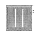
- FIG. 1 is a diagram showing electrodes formed by the electrode forming method for solar battery cells according to Embodiment 1.
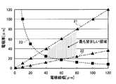
- FIG. FIG. 2 is a diagram showing a correlation between the line width and the thickness of the electrode of the solar battery cell according to Embodiment 1.
- FIG. 3 is a diagram illustrating an example of a general work process of the screen printing method.
- FIG. 4 is a diagram illustrating a configuration example of the screen plate.
- FIG. 5 is a diagram showing a flow of a method for forming an electrode of a solar battery cell according to Embodiment 1.
- FIG. 6 is a diagram illustrating a method for forming an electrode of a solar battery cell according to the second embodiment.
- FIG. 7 is a diagram illustrating a method for forming an electrode of a solar battery cell according to Embodiment 3.
- FIG. FIG. 1 is a diagram showing electrodes formed by the electrode forming method for solar battery cells according to Embodiment 1 of the present invention.
- the grid electrode 24 and the bus electrode 25 are disposed on the light receiving surface of the substrate 6 of the solar cell so as to be orthogonal to each other.
- the line width of the grid electrode 24 according to the present embodiment is preferably 10 to 90 ⁇ m, and more preferably 40 to 80 ⁇ m.
- the line width of the grid electrode 24 is preferably 10 to 90 ⁇ m because it is difficult to form an electrode with a line width of less than 10 ⁇ m from the viewpoint of processing accuracy due to problems such as disconnection in current general screen printing machines.
- the line width is increased, the light receiving area cannot be secured. With the progress of conventional screen printing methods, subdivision is gradually possible, and if the width is 40 ⁇ m or more, a practical electrode pattern can be formed without disconnection.
- a line width that can secure a light receiving area a line width of 40 to 80 ⁇ m is particularly desirable.
- the thickness of the grid electrode 24 has an appropriate value depending on the line width, but is about 0.3 to 1.0 in terms of aspect ratio (thickness / width).
- the required aspect ratio differs depending on the designed line width. However, if the aspect ratio is in the range of about 0.3 to 1.0, the resistance value of the electrode itself can be reduced without disconnection. The material is stable at the original value, and the formed electrode pattern does not collapse or the adhesion strength does not decrease. Thereby, the yield of a photovoltaic cell can be improved.
- an electrode having a line width of 10 to 90 ⁇ m when the aspect ratio is 0.3 or less, an increase in the disconnection probability due to a decrease in the electrode thickness or an increase in electrode resistance due to a decrease in the electrode cross-sectional area occurs.
- the electrode structure is excessively speci fi c, and particularly in the case of an ultra fine line width of 50 ⁇ m or less, the formed electrode pattern collapses or the adhesion strength of the grid electrode. There is a possibility that the probability of occurrence of the decrease will increase and it will not be possible to serve as an electrode.
- a resin that can be used at present is a resin containing silver. If the cross-sectional area of the silver electrode falls below a certain value, it affects the characteristics of the solar cell. As the resistance value of the electrode increases. Therefore, an electrode having a shape satisfying the range of a line width of 10 to 90 ⁇ m and an aspect ratio (thickness / width) of 0.3 to 1.0 can be adopted as an actual electrode when the cross-sectional area is small. It can be difficult. For this reason, it is preferable that the grid electrode 24 has a cross-sectional area of a certain value or more.
- FIG. 2 shows a correlation between the line width and the thickness of the electrode of the solar battery cell according to the present embodiment.
- the grid electrode 24 preferably has a line width of 10 to 90 ⁇ m, an aspect ratio (thickness / width) of 0.3 to 1, and a cross-sectional area of a certain value or more, and more preferably an electrode width of 40 to 80 ⁇ m. Therefore, in FIG. 2, between the line 21 indicating the aspect ratio 1 and the line 22 indicating the aspect ratio 0.3 and above the line 23 indicating that a certain electrode area has a certain value, the electrode It is most desirable to form the grid electrode 24 with a width and thickness so as to fall within a region having a width of 40 to 80 ⁇ m. Specific examples include a thickness of 40 ⁇ m / line width of 40 ⁇ m (aspect ratio of 1) and a thickness of 30 ⁇ m / line width of 80 ⁇ m (aspect ratio of 0.375).
- the ink paste it is necessary for the ink paste to pass through the screen mesh, and it is an ink paste that secures the fluidity of the screen mesh so as not to be clogged. It was extremely difficult to make it 3 or more.
- the electrode pattern of the grid electrode is printed and dried using a conventional screen printing method, and then the dried electrode is used using a screen plate having a narrower line width than the screen plate used first.
- An electrode having a desired line width and thickness is formed by printing, drying and firing on the pattern.
- an electrode pattern with a narrow line width can be formed by the first printing, but it cannot be printed to a desired thickness
- the desired electrode is finally obtained by making up for the insufficient thickness by the second printing.
- the second printing uses a screen plate with a narrower line width than the first printing, so the electrode width does not widen when using the same plate, and the line width specified in the first printing is not changed. Only the thickness can be formed thick.
- this method is not limited to the two-time stacking, and the number of times may be further repeated as long as a screen plate having a thinner line width than the previous one is used.
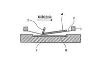
- FIG. 3 shows an example of a general work process of the screen printing method. Screen printing is performed by using a printing plate frame 1 (screen plate) on which a screen mesh 2 is stretched and a squeegee 5.
- a printing plate frame 1 screen plate
- a screen mesh 2 is stretched and a squeegee 5.
- Fig. 4 shows the configuration of the screen version.
- the screen mesh 2 is fixed to the printing plate frame 1 in a state where the screen mesh 2 is pulled in all directions and is not loosened.
- a plate film 3 is formed on the screen mesh 2, and mesh portions other than necessary image lines (here, shapes corresponding to the grid electrodes 24 and the bus electrodes 25) are closed.
- the ink paste 4 is put into the printing plate frame 1 and spread on the screen mesh 2 on the screen plate set in the screen printing machine. Furthermore, the squeegee 5 is moved while pressurizing the inner surface of the screen plate with the squeegee 5. As a result, the ink paste 4 passes through the screen mesh 2 where there is no plate film 3 and is pushed out onto the substrate 6 placed on the stage 7 and placed under the plate. The electrode pattern is printed with. The electrode pattern printed on the substrate 6 is baked after drying to become an electrode.
- FIG. 5 is a diagram showing a flow of the electrode forming method of the solar battery cell according to the present embodiment.
- the process up to the drying step is performed by the same screen printing method as in the prior art, and the electrode pattern 8 is formed of a resin containing a conductor (FIG. 5A).
- a screen plate 1 having a narrower line width than that used for the first printing is set on the substrate.
- the ink paste 4 is put in the plate frame and spread on the screen mesh.
- the ink paste used for the second printing may be the same as that used for the first printing, or may be used exclusively for the second printing (FIG. 5B).
- the squeegee 5 is moved while pressurizing the inner surface of the screen plate 1 with the squeegee 5 which is a rubber plate (FIG. 5C).
- the ink paste 4 passes through the screen mesh 2 where the plate film 3 does not exist, and is pushed onto the electrode pattern 8 of the substrate 6 placed on the stage 7 and placed under the screen plate 1 (FIG. 5 ( d)).
- the electrode pattern printed in a superimposed manner is baked after being dried to form an electrode.
- the line width of the first screen plate is 60 ⁇ m and the line width of the second screen plate is 20 ⁇ m. Version specifications other than the line width are optimized for each.
- the finished electrode line width for the first time was 80 ⁇ m
- the finished electrode line width when printed with the screen plate for the second printing alone was less than 30 ⁇ m. Therefore, even if a positional deviation of 25 ⁇ m occurs between the first printed / dried substrate and the second printing screen plate, the line width does not increase. In fact, no increase in line width was observed in the plane of the substrate on which the electrode patterns were printed using these screen plates.
- the first electrode thickness was 22 ⁇ m
- the electrode thickness was 8 ⁇ m. These figures are reasonable because the aspect ratio obtained with conventional screen printing methods is less than 0.3.
- the electrode thickness actually obtained was 28 ⁇ m, and a desired electrode could be obtained with an aspect ratio of 0.3 or more.
- the current value per unit area is improved by 0.4 mA in comparison between the conventional solar cell in which the electrode is formed by only one printing and the solar cell manufactured by using the method of the present embodiment.
- the photoelectric conversion efficiency per substrate was improved by about 0.3%. That is, the energy consumed by the resistance of the grid electrode itself can be reduced.
- solar cells can be manufactured using the same production line as before if the printing / drying process is performed a plurality of times. Moreover, if only an apparatus related to the printing / drying process is added, solar cells can be produced without reducing the production capacity. In any case, since the know-how of the screen printing method already obtained can be utilized, it is advantageous for the production of solar cells.
- the first and second electrode patterns are created on the same plate using a screen plate printed on two sheets, and printing is performed using the same ink paste while matching the timing of drying.
- the same production capacity as before can be maintained.
- an electrode having a thin line width and a large thickness can be formed without requiring an advanced manufacturing technique.
- the electrode pattern dimensions are on the order of several tens of ⁇ m, and it is sufficient that the accuracy is in the order of microns on the device characteristics.
- processing that satisfies such conditions can be easily performed. Can be realized.
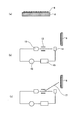
- FIG. FIG. 6 is a diagram showing a method for forming an electrode of a solar battery cell according to Embodiment 2 of the present invention. Processing up to the firing step is performed by the same screen printing method as in the prior art (FIG. 6A).
- the electrode pattern that has been fired by screen printing is connected to the cathode side of the power source, and the substrate 6 is immersed in the solution 10 in which the metal is dissolved. To do.
- a metal plate 9 is connected to the anode side of the power source, and is similarly immersed in the solution 10 to pass a current under predetermined conditions (FIG. 6B).
- the metal ions contained in the solution 10 are reduced, and the metal film 11 is deposited on the electrode pattern (FIG. 6C).
- the substrate 6 is placed so that the electrode pattern faces the opposite side of the metal plate 9, but the orientation is arbitrary as long as the metal film 11 can be uniformly deposited on the electrode pattern. .
- the grid electrode is printed and baked by using a screen printing method as usual, and then temporarily formed, and then the same or different metal as the electrode material is grown on the electrode in a liquid phase.
- a screen printing method as usual, and then temporarily formed, and then the same or different metal as the electrode material is grown on the electrode in a liquid phase.
- an electrode having a desired line width and thickness is formed.
- it is possible to form an electrode pattern with a thin line width by screen printing it is not possible to increase the thickness to the desired thickness, so by compensating for the insufficient thickness by liquid phase growth of the metal, the desired line width, Thick electrodes can be formed.
- a metal film is coated and grown in a liquid phase on the electrode pattern of a grid electrode that is thin and thin by screen printing, and the metal film grows selectively only in the electrode pattern portion. Therefore, alignment as in the first embodiment in which screen printing is performed twice is unnecessary.
- the electrode line width after printing is 80 ⁇ m and the metal film is 5 ⁇ m
- the shape at the time of printing finish is an electrode line width of 80 ⁇ m and an electrode thickness of 22 ⁇ m, as in the first printing finish in the first embodiment.
- the electrode line width after coating is 85 ⁇ m
- the electrode thickness is 27 ⁇ m
- a desired electrode pattern can be obtained with an aspect ratio of 0.3 or more. I was able to.
- the current value per unit area is 0.7 mA in comparison between the conventional solar cell in which the electrode pattern is formed by only one printing and the solar cell manufactured by using the method of the present embodiment.
- the photoelectric conversion efficiency per substrate was improved by about 0.5%. That is, the energy consumed by the resistance of the grid electrode itself can be reduced.
- a solar battery cell with improved photoelectric conversion efficiency can be manufactured by adding only a liquid phase metal film coating step to the conventional manufacturing method.
- this method increases the line width by the thickness of the metal film compared to the printing / firing method, but the resistance value of the electrode itself can be kept low by covering it with a dense metal film. Great effect on performance improvement.
- the metal coated on the electrode is limited to a specific type as long as it can be grown in a liquid phase (Au, Ag, Pt, Cu, Ni, Zn, Pd, etc.).
- the metal may be the same as or different from the metal used for screen printing.
- an electrode having a thin line width and a large thickness can be formed without requiring an advanced manufacturing technique. Productivity comparable to that can be realized.
- FIG. 7 is a diagram showing a method for forming an electrode of a solar battery cell according to Embodiment 3 of the present invention. Processing up to the drying step is performed by a screen printing method similar to the conventional one (FIG. 7A). This substrate is set in an apparatus capable of directly drawing at high speed using a fast-drying metal-containing ink. The metal-containing ink is pressurized from the ink tank 15 through the pump 16 and reaches the ink head 12 to be ejected from the ink head 12 as minute ink droplets 17 (FIG. 7B).
- the ink droplet 17 pushed out from the ink head 12 is charged by the deflection electrode 13 and at the same time, the trajectory is bent as necessary, and landed on a desired position (on the electrode pattern) of the substrate 6 (FIG. 7 (c). )). After the electrode patterns are drawn in an overlapping manner, the substrate 6 is baked. In order to prevent ink clogging, the ink droplets 17 are always ejected from the ink head 12, and normally, the ink droplets 17 are collected from the ink collection port 14 and sent to the ink tank 15 again. It is preferable to adopt a method in which only the deflection electrode 13 changes the trajectory of the ink droplet 17. By collecting the ink droplets 17, the metal-containing ink can be reused to reduce the environmental load.
- the electrode pattern of the grid electrode is printed and dried using a screen printing method as usual, and then a high-viscosity and quick-drying metal-containing ink is printed on the dried electrode pattern at high speed.
- a desired electrode pattern is formed by direct drawing and firing later.
- screen printing can form electrodes with narrow line widths, it cannot be printed as thick as desired, so the final thickness can be compensated by direct drawing of high-viscosity, quick-drying metal-containing ink.
- an electrode having a desired line width and thickness can be formed.
- the alignment between the dried electrode after screen printing and the line drawing can be controlled by the voltage applied to the deflection electrode, and the alignment accuracy is approximately ⁇ 10 ⁇ m.
- the electrode line width after printing is 80 ⁇ m and the amount of ink droplets is 50 pl (picoliter).
- the shape at the time of printing finish is an electrode line width of 80 ⁇ m and an electrode thickness of 22 ⁇ m, as in the first printing finish in the first embodiment.
- the shape after drawing with the fine ink droplets 17 did not change when the electrode line width was 80 ⁇ m, the electrode thickness was 27 ⁇ m, and a desired electrode pattern could be obtained with an aspect ratio of 0.3 or more.
- the current value per unit area is 0.5 mA.
- the photoelectric conversion efficiency per substrate was improved by about 0.4%. That is, the energy consumed by the resistance of the grid electrode itself can be reduced.
- the ink is extruded at a high pressure using the pump 16
- high-viscosity ink can be used, and also by rapidly extruding the ink, quick-drying ink can be used.
- the ink droplets 17 produced by the ink head 12 can be generated at a rate of 100 droplets or more per second, drawing can be performed at high speed, and productivity is very high as in screen printing.
- the metal contained in the ink is a metal (Au, Ag, Pt, Cu, Ni, Zn, which can be uniformly dispersed in the fast-drying ink and has excellent electrical conductivity.
- Pd is not limited to a specific type. If high productivity (manufacturing speed) is unnecessary, it is possible to draw a line by a dispensing method.
- an electrode having a thin line width and a large thickness can be formed without requiring an advanced manufacturing technique. Productivity comparable to that can be realized.
- the method for forming an electrode of a solar battery cell according to the present invention is useful in that an electrode having a thin line width and a large thickness can be easily formed at a speed comparable to that of a conventional screen printing method. .
Landscapes
- Engineering & Computer Science (AREA)
- Life Sciences & Earth Sciences (AREA)
- Sustainable Development (AREA)
- Sustainable Energy (AREA)
- Physics & Mathematics (AREA)
- Condensed Matter Physics & Semiconductors (AREA)
- Electromagnetism (AREA)
- General Physics & Mathematics (AREA)
- Computer Hardware Design (AREA)
- Microelectronics & Electronic Packaging (AREA)
- Power Engineering (AREA)
- Photovoltaic Devices (AREA)
Abstract
La présente invention concerne : un procédé de formation d'une électrode de cellule solaire, permettant à une électrode ayant une largeur de trait étroite et une grande épaisseur de pouvoir être aisément formée à une vitesse comparable aux vitesses des procédés de sérigraphie classiques ; l'invention concerne également une cellule solaire. L'invention concerne spécifiquement un procédé de formation d'une électrode de cellule solaire, comprenant : une étape d'impression, permettant de former sur un côté de surface recevant la lumière d'une cellule solaire un motif de résine contenant un conducteur ayant la forme d'une électrode par sérigraphie d'une résine contenant un conducteur en utilisant une planche tramée pourvue d'un masque doté d'une ouverture ayant la forme d'une électrode ; une étape de séchage, permettant de sécher le motif de résine contenant un conducteur ; et une étape de cuisson, permettant de cuire le motif de résine contenant un conducteur. L'étape d'impression et l'étape de séchage sont réalisées plusieurs fois, tout en réduisant la largeur d'ouverture du masque, de façon à stratifier une pluralité de motifs de résine contenant un conducteur, puis les motifs de résine contenant un conducteur sont cuits, formant ainsi une électrode.
Priority Applications (1)
| Application Number | Priority Date | Filing Date | Title |
|---|---|---|---|
| PCT/JP2010/054033 WO2011111192A1 (fr) | 2010-03-10 | 2010-03-10 | Procédé de formation d'électrode de cellule solaire, et cellule solaire |
Applications Claiming Priority (1)
| Application Number | Priority Date | Filing Date | Title |
|---|---|---|---|
| PCT/JP2010/054033 WO2011111192A1 (fr) | 2010-03-10 | 2010-03-10 | Procédé de formation d'électrode de cellule solaire, et cellule solaire |
Publications (1)
| Publication Number | Publication Date |
|---|---|
| WO2011111192A1 true WO2011111192A1 (fr) | 2011-09-15 |
Family
ID=44563034
Family Applications (1)
| Application Number | Title | Priority Date | Filing Date |
|---|---|---|---|
| PCT/JP2010/054033 WO2011111192A1 (fr) | 2010-03-10 | 2010-03-10 | Procédé de formation d'électrode de cellule solaire, et cellule solaire |
Country Status (1)
| Country | Link |
|---|---|
| WO (1) | WO2011111192A1 (fr) |
Cited By (2)
| Publication number | Priority date | Publication date | Assignee | Title |
|---|---|---|---|---|
| WO2017013866A1 (fr) * | 2015-07-22 | 2017-01-26 | 信越化学工業株式会社 | Machine d'impression sérigraphique, procédé d'impression sérigraphique et procédé de formation d'électrode pour cellule solaire |
| WO2018109849A1 (fr) | 2016-12-13 | 2018-06-21 | 信越化学工業株式会社 | Cellule solaire de type à électrode de surface arrière hautement efficace, module de cellules solaires et système de génération d'énergie solaire |
Citations (7)
| Publication number | Priority date | Publication date | Assignee | Title |
|---|---|---|---|---|
| JPH0563218A (ja) * | 1991-08-30 | 1993-03-12 | Canon Inc | 太陽電池及びその製造方法 |
| JPH06318724A (ja) * | 1993-05-07 | 1994-11-15 | Canon Inc | 電極及び光起電力素子 |
| JPH11103084A (ja) * | 1997-09-26 | 1999-04-13 | Sanyo Electric Co Ltd | 太陽電池素子の製造方法及び太陽電池素子 |
| JP2005353691A (ja) * | 2004-06-08 | 2005-12-22 | Sharp Corp | 電極、太陽電池、これらの製造方法 |
| JP2007134387A (ja) * | 2005-11-08 | 2007-05-31 | Sharp Corp | 光電変換素子およびその電極形成方法 |
| WO2009041182A1 (fr) * | 2007-09-27 | 2009-04-02 | Murata Manufacturing Co., Ltd. | Pâte d'électrode à base de ag, cellule de batterie solaire et procédé de fabrication de la cellule de batterie solaire |
| JP2009283558A (ja) * | 2008-05-20 | 2009-12-03 | Sharp Corp | 太陽電池およびその製造方法、それを備えた太陽電池システム |
-
2010
- 2010-03-10 WO PCT/JP2010/054033 patent/WO2011111192A1/fr active Application Filing
Patent Citations (7)
| Publication number | Priority date | Publication date | Assignee | Title |
|---|---|---|---|---|
| JPH0563218A (ja) * | 1991-08-30 | 1993-03-12 | Canon Inc | 太陽電池及びその製造方法 |
| JPH06318724A (ja) * | 1993-05-07 | 1994-11-15 | Canon Inc | 電極及び光起電力素子 |
| JPH11103084A (ja) * | 1997-09-26 | 1999-04-13 | Sanyo Electric Co Ltd | 太陽電池素子の製造方法及び太陽電池素子 |
| JP2005353691A (ja) * | 2004-06-08 | 2005-12-22 | Sharp Corp | 電極、太陽電池、これらの製造方法 |
| JP2007134387A (ja) * | 2005-11-08 | 2007-05-31 | Sharp Corp | 光電変換素子およびその電極形成方法 |
| WO2009041182A1 (fr) * | 2007-09-27 | 2009-04-02 | Murata Manufacturing Co., Ltd. | Pâte d'électrode à base de ag, cellule de batterie solaire et procédé de fabrication de la cellule de batterie solaire |
| JP2009283558A (ja) * | 2008-05-20 | 2009-12-03 | Sharp Corp | 太陽電池およびその製造方法、それを備えた太陽電池システム |
Cited By (10)
| Publication number | Priority date | Publication date | Assignee | Title |
|---|---|---|---|---|
| WO2017013866A1 (fr) * | 2015-07-22 | 2017-01-26 | 信越化学工業株式会社 | Machine d'impression sérigraphique, procédé d'impression sérigraphique et procédé de formation d'électrode pour cellule solaire |
| CN107848314A (zh) * | 2015-07-22 | 2018-03-27 | 信越化学工业株式会社 | 丝网印刷机、丝网印刷方法及太阳能电池的电极形成方法 |
| KR20180032554A (ko) * | 2015-07-22 | 2018-03-30 | 신에쓰 가가꾸 고교 가부시끼가이샤 | 스크린 인쇄기, 스크린 인쇄 방법 및 태양전지의 전극 형성 방법 |
| JPWO2017013866A1 (ja) * | 2015-07-22 | 2018-04-19 | 信越化学工業株式会社 | スクリーン印刷機、スクリーン印刷方法及び太陽電池の電極形成方法 |
| JP2019214207A (ja) * | 2015-07-22 | 2019-12-19 | 信越化学工業株式会社 | スクリーン印刷機、スクリーン印刷方法及び太陽電池の電極形成方法 |
| US11101391B2 (en) | 2015-07-22 | 2021-08-24 | Shin-Etsu Chemical Co., Ltd. | Screen printing apparatus, screen printing method, and electrode formation method of solar battery |
| KR102393056B1 (ko) * | 2015-07-22 | 2022-04-29 | 신에쓰 가가꾸 고교 가부시끼가이샤 | 스크린 인쇄기, 스크린 인쇄 방법 및 태양전지의 전극 형성 방법 |
| WO2018109849A1 (fr) | 2016-12-13 | 2018-06-21 | 信越化学工業株式会社 | Cellule solaire de type à électrode de surface arrière hautement efficace, module de cellules solaires et système de génération d'énergie solaire |
| KR20190089842A (ko) | 2016-12-13 | 2019-07-31 | 신에쓰 가가꾸 고교 가부시끼가이샤 | 고효율 이면 전극형 태양전지 셀, 태양전지 모듈, 및 태양광 발전 시스템 |
| US10896989B2 (en) | 2016-12-13 | 2021-01-19 | Shin-Etsu Chemical Co., Ltd. | High efficiency back contact type solar cell, solar cell module, and photovoltaic power generation system |
Similar Documents
| Publication | Publication Date | Title |
|---|---|---|
| CN105895853B (zh) | 一种储能器件及其制备方法 | |
| JP6525944B6 (ja) | リチウムイオン電池電極フィルムの多孔率の変化を生み出す方法 | |
| Mariani et al. | The role of printing techniques for large-area dye sensitized solar cells | |
| CN104538496B (zh) | 一种高效硅异质结太阳能电池电镀电极制备方法 | |
| CN101743639B (zh) | 用于半导体部件的接触结构及其制造方法 | |
| TW200918325A (en) | AEROSOL JET® printing system for photovoltaic applications | |
| KR101377210B1 (ko) | 전기 도금을 이용한 다공성 박막의 제조방법 | |
| CN102555562A (zh) | 一种太阳能电池片的印刷工艺 | |
| JP5288633B2 (ja) | 太陽電池の電極形成システムおよび太陽電池の電極形成方法 | |
| CN104659134B (zh) | 形成导电电极图案的方法和制造包括其的太阳电池的方法 | |
| EP2936560B1 (fr) | Procédé de fabrication d'un ensemble de cellules solaires à couche mince | |
| CN105120599A (zh) | 一种线路板的孤立线的阻抗控制方法 | |
| CN110678004A (zh) | 一种充电桩用pcb板的制作方法 | |
| WO2011111192A1 (fr) | Procédé de formation d'électrode de cellule solaire, et cellule solaire | |
| JP6439641B2 (ja) | 導電性パターンの形成方法及び導電性パターン | |
| CN110190140A (zh) | 可溶性掩膜真空镀制备光伏电池栅线电极的方法 | |
| CN106981418A (zh) | 电极图案的形成方法及电子元器件的制造方法 | |
| DE102009053416A1 (de) | Verfahren zur Herstellung und Verschaltung einer Solarzellanordnung | |
| WO2013120013A1 (fr) | Appareil d'impression sérigraphique comportant des barres de support et leurs procédés d'utilisation | |
| CN102582261B (zh) | 喷墨头的制造方法及电极形成方法 | |
| CN103192619B (zh) | 一种太阳能电池片的印刷方法 | |
| JP2005166914A (ja) | 太陽電池の製造方法 | |
| CN102821548A (zh) | 一种防止静电喷涂掉板的板边图形工具制作方法 | |
| CN208466367U (zh) | 一种涂布机 | |
| JPH0897448A (ja) | 太陽電池の電極形成方法 |
Legal Events
| Date | Code | Title | Description |
|---|---|---|---|
| 121 | Ep: the epo has been informed by wipo that ep was designated in this application |
Ref document number: 10847422 Country of ref document: EP Kind code of ref document: A1 |
|
| NENP | Non-entry into the national phase |
Ref country code: DE |
|
| 122 | Ep: pct application non-entry in european phase |
Ref document number: 10847422 Country of ref document: EP Kind code of ref document: A1 |
|
| NENP | Non-entry into the national phase |
Ref country code: JP |