WO2011108476A1 - 薄膜太陽電池、その製造方法、および薄膜太陽電池製造用のレーザ加工装置 - Google Patents
薄膜太陽電池、その製造方法、および薄膜太陽電池製造用のレーザ加工装置 Download PDFInfo
- Publication number
- WO2011108476A1 WO2011108476A1 PCT/JP2011/054446 JP2011054446W WO2011108476A1 WO 2011108476 A1 WO2011108476 A1 WO 2011108476A1 JP 2011054446 W JP2011054446 W JP 2011054446W WO 2011108476 A1 WO2011108476 A1 WO 2011108476A1
- Authority
- WO
- WIPO (PCT)
- Prior art keywords
- laser
- processing line
- processing
- layer
- substrate
- Prior art date
- Legal status (The legal status is an assumption and is not a legal conclusion. Google has not performed a legal analysis and makes no representation as to the accuracy of the status listed.)
- Ceased
Links
Images

















Classifications
-
- H—ELECTRICITY
- H10—SEMICONDUCTOR DEVICES; ELECTRIC SOLID-STATE DEVICES NOT OTHERWISE PROVIDED FOR
- H10F—INORGANIC SEMICONDUCTOR DEVICES SENSITIVE TO INFRARED RADIATION, LIGHT, ELECTROMAGNETIC RADIATION OF SHORTER WAVELENGTH OR CORPUSCULAR RADIATION
- H10F19/00—Integrated devices, or assemblies of multiple devices, comprising at least one photovoltaic cell covered by group H10F10/00, e.g. photovoltaic modules
- H10F19/30—Integrated devices, or assemblies of multiple devices, comprising at least one photovoltaic cell covered by group H10F10/00, e.g. photovoltaic modules comprising thin-film photovoltaic cells
- H10F19/31—Integrated devices, or assemblies of multiple devices, comprising at least one photovoltaic cell covered by group H10F10/00, e.g. photovoltaic modules comprising thin-film photovoltaic cells having multiple laterally adjacent thin-film photovoltaic cells deposited on the same substrate
- H10F19/33—Patterning processes to connect the photovoltaic cells, e.g. laser cutting of conductive or active layers
-
- Y—GENERAL TAGGING OF NEW TECHNOLOGICAL DEVELOPMENTS; GENERAL TAGGING OF CROSS-SECTIONAL TECHNOLOGIES SPANNING OVER SEVERAL SECTIONS OF THE IPC; TECHNICAL SUBJECTS COVERED BY FORMER USPC CROSS-REFERENCE ART COLLECTIONS [XRACs] AND DIGESTS
- Y02—TECHNOLOGIES OR APPLICATIONS FOR MITIGATION OR ADAPTATION AGAINST CLIMATE CHANGE
- Y02E—REDUCTION OF GREENHOUSE GAS [GHG] EMISSIONS, RELATED TO ENERGY GENERATION, TRANSMISSION OR DISTRIBUTION
- Y02E10/00—Energy generation through renewable energy sources
- Y02E10/50—Photovoltaic [PV] energy
Definitions
- the present invention relates to a thin film solar cell in which a plurality of processing lines are formed in each of a plurality of layers formed on a substrate, a manufacturing method thereof, and a laser processing apparatus for manufacturing a thin film solar cell.
- a transparent conductive film 101 is formed on the substrate 100.
- a plurality of processing lines 110 are formed on the transparent conductive film 101.
- a photoelectric conversion layer 102 is formed so as to cover the transparent conductive film 101 and the processing line 110.
- a plurality of processing lines 120 are formed on the photoelectric conversion layer 102.
- the back electrode layer 103 is formed so as to cover the photoelectric conversion layer 102 and the processing line 120.
- a plurality of processing lines 130 also referred to as separation lines
- a plurality of solar cells 108 connected in series are formed on the substrate 100.
- the integration interval P of the solar cells 108 is about 5 mm to about 15 mm.
- the region W1 including the processing lines 110, 120, and 130 does not contribute to power generation.
- the photoelectric conversion layer (102) or the back electrode layer (103) is formed on the substrate 100 at a high temperature.
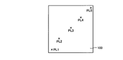
- the relationship between the elapsed time after the photoelectric conversion layer 102 was formed on the substrate 100 and the temperature change (room temperature environment) at any position PL1 to PL5 on the substrate 100 was measured.
- a glass substrate 1000 mm ⁇ 1400 mm ⁇ 4 mm was used.
- photoelectric conversion layer 102 is formed on transparent conductive film 101 at a high temperature.
- a temperature difference similar to the above occurs between the outer peripheral side of the substrate 100 and the center side of the substrate 100. Due to the temperature difference, a difference occurs in the degree of thermal expansion between the outer peripheral side of the substrate 100 and the center side of the substrate 100.
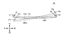
- the plurality of processing lines 110 formed on the transparent conductive film 101 are curved for a predetermined time.
- the back electrode layer 103 is also formed at a high temperature, the plurality of processing lines 120 formed on the photoelectric conversion layer 102 are curved for a predetermined time.
- the processing line 120 may be formed to overlap the processing line 110 due to the curvature.
- the characteristics of the thin film solar cell 1000 may be deteriorated or poor electrical connection may occur (the same applies to the processing line 120 and the processing line 130).
- the photoelectric conversion layer 102 is an important layer that affects the characteristics of the thin film solar cell, and it is extremely important to perform the next step in a short time after the formation of the photoelectric conversion layer 102.
- the present invention provides a thin-film solar cell in which a plurality of processing lines are formed at predetermined intervals and without overlapping each other on each of a plurality of layers formed on a substrate without reducing manufacturing efficiency, a method for manufacturing the same, And it aims at providing the laser processing apparatus for thin film solar cell manufacture.
- a laser processing apparatus for manufacturing a thin-film solar cell according to the first aspect of the present invention is stacked above the first layer so as to follow a plurality of first processing lines formed side by side on the first layer on the substrate.
- a laser processing apparatus for manufacturing a thin-film solar cell that forms a second processing line in the second layer formed, and a stage and a laser beam irradiated to the substrate placed on the stage and on one side
- a laser head relatively movable toward the other side; a first measuring device disposed on the one side of the laser head and movable relative to the substrate together with the laser head; and the laser head
- the second measuring device is disposed on the other side of the laser, and is movable relative to the substrate together with the laser head.
- the first measuring device measures positional information of the first first processing line in front of the moving direction of the laser head, and the control device is configured such that the first second processing line is the first first.
- the second measuring device measures the position information of the second first processing line in front of the moving direction of the laser head, and the control device is configured such that the second second processing line is the second second.
- the irradiation position of the laser beam is controlled based on the position information of the second first processing line so as to be formed along one processing line.
- a laser processing apparatus for manufacturing a thin-film solar cell according to a second aspect of the present invention is stacked above the first layer so as to follow a plurality of first processing lines formed side by side on the first layer on the substrate.
- a laser processing apparatus for manufacturing a thin-film solar cell that forms a second processing line in the second layer formed, and a stage and a laser beam irradiated to the substrate placed on the stage and on one side
- a laser head relatively movable toward the other side, a measuring device arranged on the one side of the laser head and movable relative to the substrate together with the laser head, and a control device, And when the laser head moves toward the one side, the measuring device measures position information of the first first processing line in front of the moving direction of the laser head, and the control device The irradiation position of the laser beam is controlled based on the position information of the first processing line so that the second processing line is formed along the first processing line.
- the control device causes the first first first so that the second second processing line is formed along
- a laser processing apparatus for manufacturing a thin film solar cell according to a third aspect of the present invention is stacked above the first layer so as to follow a plurality of first processing lines formed side by side on the first layer on the substrate.
- a laser processing apparatus for manufacturing a thin-film solar cell that forms a second processing line in the second layer formed, and a stage and a laser beam irradiated to the substrate placed on the stage and on one side
- a laser head that is relatively movable toward the other side, and a measuring device that is disposed on a side where the first processing lines of the laser head are arranged and is relatively movable with respect to the substrate together with the laser head;
- a control device, and the laser head irradiates the laser beam while moving toward the one side or the other side to form the second processing line along the first processing line.
- the measuring device measures positional information of the second first processing line located on the side of the laser head in the direction in which the first processing lines are arranged, and the laser head is positioned on the one side or the other side.
- the control device is configured to control the second processing line based on the position information of the second first processing line so that the second processing line is formed along the second first processing line.
- the irradiation position of the laser beam is controlled.
- a method of manufacturing a thin-film solar cell includes a first step of forming a first processing line by scanning a laser beam with respect to a first layer on a substrate, the first layer, A second step of forming a second layer above the first processing line; and scanning the laser beam toward a predetermined direction with respect to the second layer, and the front of the laser beam in the scanning direction.
- the position information of the first processing line is measured, and the irradiation position of the laser beam is controlled based on the position information so that the second processing line is formed on the second layer along the first processing line.
- a method for manufacturing a thin-film solar cell includes a first processing line formed in a plurality of rows by scanning a laser beam with respect to a first layer on a substrate, and the first layer. And a first step of preparing a laminate having a second layer formed above the first processing line, and the first layer while scanning the laser beam toward one side with respect to the second layer.
- the two layers are irradiated with the laser light, the positional information of the first processing line is measured in front of the scanning direction of the laser light, and the first second processing line is first on the second layer.
- a method for manufacturing a thin-film solar cell includes a first processing line formed in a plurality of rows by scanning a laser beam on a first layer on a substrate, and the first layer. And a first step of preparing a laminate having a second layer formed above the first processing line, and the laser on the second layer while scanning the laser beam on the second layer.
- a third step of forming a second second processing line in the second layer along the second layer Provided.
- the second processing line is stacked above the first layer so as to be along the first processing line formed in the first layer on the substrate.
- a method of manufacturing a thin-film solar cell formed on the second layer wherein the first step of measuring the position information of the first processing line outside the laser processing apparatus, and the substrate with respect to the laser processing apparatus A second step of relatively moving the substrate to place the substrate inside the laser processing apparatus; and scanning the laser beam with respect to the second layer, and the second processing line on the second layer.
- the thin-film solar cell based on the eighth aspect of the present invention is manufactured using a laser processing apparatus for manufacturing a thin-film solar cell based on the first aspect.
- the thin-film solar cell based on the ninth aspect of the present invention is manufactured using the method for manufacturing a thin-film solar cell based on the fourth aspect.
- a thin film solar cell in which a plurality of processing lines are formed at predetermined intervals and without overlapping each other on each of the plurality of layers formed on the substrate without reducing the manufacturing efficiency, and the manufacture thereof A method and a laser processing apparatus for manufacturing a thin film solar cell can be obtained.
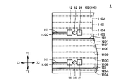
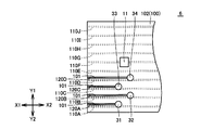
- FIG. 1 is a plan view showing an overall configuration of a laser processing apparatus for manufacturing a thin film solar cell according to Embodiment 1 (and Embodiments 2 to 6). It is a 1st top view which shows a mode that the processing line is formed in the photoelectric converting layer on a board
- FIG. 1 It is a top view which shows the positional relationship of a laser head and a measuring apparatus regarding the other form (2nd modification) of the laser processing apparatus for thin film solar cell manufacture which concerns on Embodiment 1.
- FIG. 2 It is a top view which shows that the positional relationship of a laser head and a measuring apparatus shifted
- FIG. The top view which shows the processing line formed in the state from which the positional relationship of a laser head and a measuring apparatus shifted
- FIG. It is a 1st top view which shows a mode that the processing line is formed in the photoelectric converting layer on a board
- FIG. It is a 2nd top view which shows a mode that the processing line is formed in the photoelectric converting layer on a board
- FIG. It is a 3rd top view which shows a mode that the processing line is formed in the photoelectric converting layer on a board
- FIG. It is a top view which shows the area
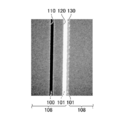
- FIG. It is an enlarged plan view (photograph) which shows the thin film solar cell manufactured based on the Example of the laser processing apparatus for thin film solar cell manufacture which concerns on Embodiment 3.
- FIG. It is an enlarged plan view (photograph) which shows the thin film solar cell manufactured based on the comparative example regarding the laser processing apparatus for thin film solar cell manufacture which concerns on Embodiment 3.
- FIG. 1st top view which shows a mode that the processing line is formed in the photoelectric converting layer on a board
- FIG. It is a 2nd top view which shows a mode that the processing line is formed in the photoelectric converting layer on a board
- FIG. 1st top view which shows a mode that the processing line is formed in the photoelectric converting layer on a board
- FIG. 2nd top view which shows a mode that the processing line is formed in the photoelectric converting layer on a board
- FIG. 1 It is a 3rd top view which shows a mode that the processing line is formed in the photoelectric converting layer on a board
- FIG. It is a top view which shows the modification of the laser processing apparatus for thin film solar cell manufacture which concerns on Embodiment 6.
- FIG. It is a perspective view which shows the whole structure of the laser processing apparatus for thin film solar cell manufacture which concerns on Embodiment 7 (and the modification of Embodiment 7).
- FIG. It is a top view which shows that the position of the board
- FIG. It is sectional drawing which shows the structure of a general thin film solar cell. It is a top view which shows the arbitrary positions on a board
- thin film solar cells thin film solar cell manufacturing methods, and thin film solar cell manufacturing laser processing apparatuses (hereinafter sometimes simply referred to as laser processing apparatuses) according to the embodiments of the present invention, refer to the drawings. While explaining. In the description of each embodiment, when referring to the number, amount, or the like, the scope of the present invention is not necessarily limited to the number, amount, or the like unless otherwise specified. In the description of each embodiment, the same parts and corresponding parts are denoted by the same reference numerals, and redundant description may not be repeated.
- a laser processing apparatus 1 includes laser heads 31 and 32, a measurement apparatus 11 (first measurement apparatus), a measurement apparatus 21 (second measurement apparatus), measurement apparatuses 12 and 22, a head drive mechanism 71, 72, a head support device 75, fibers 81 and 82, a laser oscillator 86, a control device 80, an image processing unit 88, a base 70, a stage drive unit 74, a stage 76, and a fixing member 78.
- the laser oscillated from the laser oscillator 86 is transmitted to the laser head 31 through the fiber 81.
- the laser oscillated from the laser oscillator 86 may be transmitted to the laser head 31 by a so-called spatial transmission method.
- the laser is emitted from the laser head 31 (toward the depth side of the paper in the direction perpendicular to the paper).
- the laser is a YAG laser, a YVO4 laser, or the like.
- the measuring device 11 is arranged on one side of the laser head 31, for example, on the arrow X1 direction side.
- the measuring device 21 is arranged on the other side of the laser head 31, for example, on the arrow X2 direction side.
- the measuring devices 11 and 21 include imaging means such as a camera.
- the laser head 31 and the measuring devices 11 and 21 are supported from above (front side in the direction perpendicular to the paper surface) by the head support device 75.
- the head driving mechanism 71 moves the laser head 31 and the measuring devices 11 and 21 to the arrow Y1 direction side and the arrow Y2 direction side.
- the fiber 82, the laser head 32, the measuring devices 12 and 22, and the head driving mechanism 72 are configured in the same manner as the fiber 81, the laser head 31, the measuring devices 11 and 21, and the head driving mechanism 71.
- the substrate 100 is placed on the stage 76.
- the stage 76 may include a support pin (not shown) or the like in order to adjust the flatness of the substrate 100.
- the substrate 100 is fixed at a predetermined position by the fixing member 78.
- the stage drive unit 74 moves the stage 76 to the arrow X1 direction side and the arrow X2 direction side.
- the stage driving unit 74 can move the substrate 100 below the laser heads 31 and 32 and below the measuring devices 11, 21, 12, and 22 to the arrow X1 direction side and the arrow X2 direction side.
- the substrate 100 is prepared.
- the substrate 100 is a glass substrate having insulating properties and translucency.
- the substrate 100 moves to the arrow X2 direction side.
- a transparent conductive film 101 (first layer) (see FIG. 32) is formed on the substrate 100 by thermal CVD or sputtering.
- the transparent conductive film 101 is made of SnO 2 , ITO, ZnO, or the like.
- the substrate 100 passes below the laser heads 31 and 32 that are irradiating the laser beam.
- Laser light processes the transparent conductive film 101.
- a processing line 110 (see FIG. 32) extending along the arrow X1 and X2 directions is formed in the transparent conductive film.
- the laser heads 31 and 32 move by a predetermined distance in the direction of the arrow Y1.
- the substrate 100 moves to the arrow X2 direction side.
- the substrate 100 passes below the laser heads 31 and 32 that are irradiating the laser beam.
- another processing line 110 extending along the arrow X1 and X2 directions is formed.
- the measuring devices 11, 21, 12 and 22 may be omitted as an apparatus used for forming the processing line 110 of the transparent conductive film 101.
- the substrate 100 and the laser heads 31 and 32 repeat the above operation a plurality of times.
- a plurality of processing lines 110 extending along the arrow X1 and X2 directions are formed in the transparent conductive film 101 so as to be arranged substantially parallel to the arrow Y1 direction.
- a photoelectric conversion layer 102 (second layer) (see FIG. 32) is formed by plasma CVD or the like so as to cover the transparent conductive film 101 and the plurality of processing lines 110.
- the photoelectric conversion layer 102 includes a p layer, an i layer, and an n layer that are sequentially stacked.
- the substrate 100 on which the photoelectric conversion layer 102 is formed moves to the arrow X2 direction side.
- the substrate 100 passes below the measuring device 11.
- the measuring device 11 scans the photoelectric conversion layer 102 in the arrow X1 direction side.
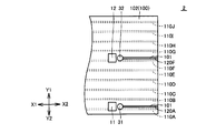
- the measuring device 11 measures position information of the processing line 110A (first first processing line) on the arrow X1 direction side of the laser head 31.
- the measuring device 11 may measure position information on the processing line 110A intermittently (partially) from the viewpoint of processing speed or information amount. For example, when the size of the substrate 100 is 1000 mm ⁇ 1400 mm, the measuring device 11 may measure position information at three or more locations or five or more locations on the processing line 110A. The number of measurement points may be selected according to the required processing accuracy (design value).
- the position information of the processing line 110A is input to the control device 80 through the image processing unit 88 (FIG. 1).
- the laser head 31 irradiates laser light.
- the laser light processes the photoelectric conversion layer 102 along the processing line 110A.
- the control device 80 (FIG. 1) controls the irradiation position of the laser beam based on the position information of the processing line 110A.
- the control device 80 controls the irradiation position of the laser beam so that the processing line 120A does not overlap with the processing line 110A.
- the control device 80 controls the irradiation position of the laser beam so that the interval between the processing line 120A and the processing line 110A is as narrow as possible (as designed).
- the control device 80 controls the irradiation position of the laser beam by moving the laser head 31 to the arrow Y1 direction side or the arrow Y2 direction side.
- a processing line 120A (first second processing line) extending along the arrow X1 and X2 direction side is formed in the photoelectric conversion layer 102.
- the irradiation position of the laser light may be controlled.
- the step of measuring the position information of the processing line 110A by the measuring device 11 and the step of controlling the irradiation position of the laser beam are as short as possible (substantially) even if they are separate steps. The same step) may be performed.
- the laser head 32 and the measuring device 21 operate in the same manner as the laser head 31 and the measuring device 11.
- the laser head 32 and the measuring device 11 form a processing line 120F that extends along the arrow X1 and X2 directions.
- the laser head 31 and the measuring devices 11 and 21 move in the direction of the arrow Y1 until they reach the side of the processing line 110B.
- the laser head 32 and the measuring devices 12 and 22 move to the arrow Y1 direction side until they reach the side of the processing line 110G.
- the substrate 100 on which the processing lines 120A and 120F are formed moves to the arrow X1 direction side.
- the substrate 100 passes below the measuring device 21.
- the measuring device 21 scans the photoelectric conversion layer 102 in the arrow X2 direction side.
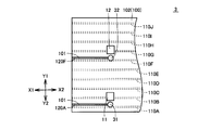
- the measuring device 21 measures position information of the processing line 110B (second first processing line) on the arrow X2 direction side of the laser head 31.
- the position information of the processing line 110B is input to the control device 80 through the image processing unit 88 (FIG. 1).
- the laser head 31 When the substrate 100 moves in the direction of the arrow X1, the laser head 31 emits laser light.
- the laser light processes the photoelectric conversion layer 102 along the processing line 110B.
- the control device 80 (FIG. 1) controls the irradiation position of the laser beam based on the position information of the processing line 110B.
- the control device 80 controls the irradiation position of the laser beam so that the processing line 120B does not overlap with the processing line 110B.
- the control device 80 controls the irradiation position of the laser beam so that the interval between the processing line 120B and the processing line 110B is as narrow as possible (as designed).
- the control device 80 controls the irradiation position of the laser beam by moving the laser head 31 to the arrow Y1 direction side or the arrow Y2 direction side.
- a processing line 120B (second second processing line) extending along the arrow X1 and X2 direction side is formed on the photoelectric conversion layer 102.
- the irradiation position of the laser light may be controlled.
- the step of measuring the position information of the processing line 110B by the measuring device 21 and the step of controlling the irradiation position of the laser beam are as short as possible (substantially) even if they are separate steps. It may be performed in the same step).
- the laser head 32 and the measuring device 22 operate in the same manner as the laser head 31 and the measuring device 21.
- the laser head 32 and the measuring device 22 form a processing line 120G extending along the arrow X1 and X2 directions.
- the laser head 31 and the measuring devices 11 and 21 repeat the above operation for the processing lines 110C to 110E.
- the laser head 32 and the measuring devices 12 and 22 repeat the above operation for the processing lines 110H to 110J.
- the thin film solar cell according to the present embodiment is obtained.
- the back electrode layer 103 is formed on the photoelectric conversion layer 102 and the second processing line 120.
- the back electrode layer 103 is formed by laminating a transparent electrode layer such as ZnO, ITO, or SnO 2 and a metal layer such as Ag or AL by a method such as sputtering or vacuum deposition.
- the back electrode layer 103 may have a thickness of about 100 nm to about 500 nm.
- a third processing line is formed on the back electrode layer 103.
- the third processing line can be formed by the same method as the second processing line described above. In forming the third processing line, either the first processing line or the second processing line may be used as the position information measurement target.
- the processing line As the processing line, the first processing line, the second processing line, and the third processing line are formed in parallel in this order. With this configuration, it is possible to electrically connect the transparent conductive film 101 of one solar battery cell and the other back electrode layer 103 adjacent to each other with the first to third processing lines interposed therebetween, and a plurality of solar batteries An integrated thin film solar cell in which cells are connected in series is obtained.
- the second process line is formed along the first first process line means the first first Not only the case where the second processing line is formed at a position close to the processing line but also the case where the second processing line is formed at a position away from the first first processing line is included.
- one of the first processing lines (the second one), which is formed side by side with the first first processing line, up to several (preferably the second) counted from the first first processing line side.
- the case where the second processing line is formed at a position close to the first processing line) is also included.
- the first processing line adjacent to the first first processing line is changed to the second first processing line. It is preferable to form a second processing line so as to be close to the line, and it is more preferable to form the second processing line so as to be close to the first first processing line.
- the measuring device 11 When the substrate 100 moves to the arrow X2 direction side, the measuring device 11 operates. When the substrate 100 moves in the direction of the arrow X1, the measuring device 21 operates. The measuring devices 11 and 21 operate according to the moving direction of the substrate 100. According to the laser processing apparatus 1, a processing line can be formed quickly.
- the processing line on the photoelectric conversion layer is formed without overlapping the processing line on the transparent conductive film.
- the processing line on the photoelectric conversion layer is formed so that the distance from the processing line on the transparent conductive film is as narrow as possible (as designed).
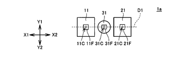
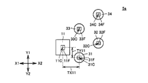
- Embodiment 1 (First Modification of Embodiment 1) With reference to FIG. 4, the laser processing apparatus 1a which concerns on the 1st modification of Embodiment 1 is demonstrated.
- an irradiation image 31F is formed on the irradiation object (transparent conductive film or the like).
- the irradiation image 31F has a center 31C.
- the measuring device 11 has an imaging range 11F on the irradiated object.
- the imaging range 11F has a center 11C.
- the measuring device 21 has an imaging range 21F on the irradiated object.
- the measuring device 21 has a center 21C.
- the center 31C of the irradiation image 31F, the center 11C of the imaging range 11F, and the center 21C of the imaging range 21F may be arranged on the same straight line D1.
- the laser head 31 and the measuring devices 11 and 21 are preferably arranged so that the straight line D1 and the moving direction of the substrate 100 (arrow X1 direction side or arrow X2 direction side) are parallel.
- the laser processing apparatus 1a can form a processing line with higher accuracy.
- the interval between the positions of the centers 11C, 21C, and 31C and the straight line D1 may be set in advance as an offset amount for the control device 80.
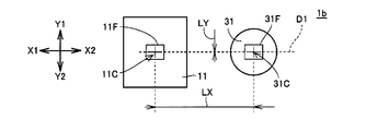
- the laser processing apparatus 1b which concerns on the 2nd modification of Embodiment 1 is demonstrated.
- the laser processing apparatus 1b may further include a correcting unit 89.
- the relative positional relationship between the laser head 31 and the measuring apparatuses 11 and 21 may be shifted. There may be a deviation in the relative positional relationship with the measuring devices 11 and 21 due to a change in the temperature of the environment in which the laser processing device 1b is installed.
- a predetermined interval LX is set between the center 31C of the laser head 31 and the center 11C of the measuring apparatus 11 on the arrow X1 and X2 direction side.
- the interval LX (FIG. 5) changes to the interval LX + ⁇ due to a predetermined external factor.
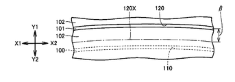
- the interval LY (FIG. 5) changes to the interval LY + ⁇ . Due to these changes, the position of the processing line to be formed also changes.
- the processing line 120 actually formed on the photoelectric conversion layer 102 is the distance ⁇ in the arrow Y1 direction side with respect to the position of the desired processing line 120X that should be originally formed on the photoelectric conversion layer 102. It is formed by shifting only.
- the correction unit 89 gives the difference to the control device 80 as an offset amount. Set as. Based on the offset amount, the control device 80 corrects the irradiation position of the laser beam.
- the correction may be performed every time one processing line is formed from the viewpoint of processing accuracy.
- the correction may be performed every time one substrate (100) is manufactured from the viewpoint of manufacturing time.
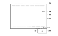
- a non-power generation region 106 is formed at the peripheral edge of the substrate 100 in the laser processing apparatus 1b.
- a power generation region 104 is formed at the center of the substrate 100.
- the correcting unit 89 may correct the irradiation position of the laser beam in the non-power generation area 106.
- the width of the non-power generation region 106 is about 5 mm to about 15 mm.
- the correcting unit 89 acquires position information of the predetermined reference point 51 on the non-power generation region 106 for securing an insulating area from the measuring device 11 (FIG. 1).
- the correction unit 89 inputs the position information of the reference point 51 (can be set at an arbitrary position) to the control device 80 (FIG. 1).
- the control device 80 controls the irradiation position of the laser beam irradiated from the laser head 31 (FIG. 1) based on the position information of the reference point 51.
- the laser beam is emitted toward the reference point 51.
- the correction unit 89 compares the position information of the reference point 51 acquired from the measuring device 11 with the actual position information of the formed processing line (point). When the position information of the reference point 51 acquired from the measuring device 11 and the actual position information of the formed processing line (point) do not match, the correction unit 89 offsets the difference to the control device 80. Enter as a quantity. Based on the offset amount, the control device 80 corrects the irradiation position of the laser beam.
- laser processing apparatus 1b may further include a dummy substrate 200.
- the correction unit 89 acquires position information of the predetermined reference point 52 on the dummy substrate 200 from the measurement apparatus 11 (FIG. 1).
- the correction means 89 inputs the position information of the reference point 52 to the control device 80 (FIG. 1).
- the control device 80 controls the irradiation position of the laser beam emitted from the laser head 31 (FIG. 1) based on the position information of the reference point 52 (can be set at an arbitrary position).
- the laser beam is emitted toward the reference point 52.
- the correction unit 89 compares the position information of the reference point 52 acquired from the measuring apparatus 11 with the actual position information of the formed processing line (point). When the position information of the reference point 52 acquired from the measuring device 11 and the actual position information of the formed processing line (point) do not match, the correction unit 89 offsets the difference to the control device 80. Enter as a quantity. Based on the offset amount, the control device 80 corrects the irradiation position of the laser beam.
- the timing for correction is preferably about once a day in consideration of device operation. However, for example, if a state in which no substrate is received from the previous process occurs, correction may be performed on the final substrate received each time. Furthermore, if the data acquisition for positional deviation correction is performed a plurality of times, the accuracy can be improved more stably.
- the laser processing apparatus 1b further includes the correcting unit 89, it is possible to stably form a processing line with higher accuracy.
- Embodiment 1 With reference to FIG. 1, in the above-described first embodiment, the description has been made based on the mode in which the substrate 100 is moved in the directions of the arrows X1 and X2.
- the substrate 100 may be fixed, and the laser heads 31, 32 and the measuring devices 11, 21, 12, 22 may be moved to the arrow X1, X2, Y1, Y2 direction side.
- the measuring devices 11 and 21 may be movable with the laser head 31 with respect to the substrate 100 or may be movable integrally with the laser head 31.
- the laser head 31 and the measuring devices 11 and 21 may be relatively movable, and may be configured to be controlled separately.
- the laser head 31 and the measuring devices 11 and 21 may be configured so that the positions of the laser head 31 and the measuring devices 11 and 21 can be finely adjusted regardless of whether they move together or move separately. All of these are the same in the relationship between the measuring devices 12 and 22 and the laser head 32.
- the laser processing apparatus 1 has been described based on the aspect in which the processing line of the photoelectric conversion layer 102 is formed with respect to the processing locus of the transparent conductive film 101.
- the laser processing apparatus 1 may form a processing line for the back electrode layer 103 (corresponding to the second layer) with respect to the processing locus of the photoelectric conversion layer 102 (corresponding to the first layer), or may be transparent conductive.
- a processing line for the back electrode layer 103 (corresponding to the second layer) may be formed with respect to the trajectory of the film 101.
- the back electrode layer 103 is configured by laminating a transparent conductive layer such as ZnO, ITO, or SnO 2 and a metal layer such as Ag or AL.
- the back electrode layer may have a thickness of about 100 nm to about 500 nm.
- the laser processing device 2 includes a measuring device 11 and a measuring device 12.
- the laser processing device 2 does not include the measuring devices 21 and 22 (see FIG. 2).
- the measuring device 11 is disposed on the arrow X1 direction (one side) of the laser head 31.
- the measuring device 12 is disposed on the arrow X1 direction side of the laser head 32.
- the substrate 100 is prepared.
- a transparent conductive film 101 is formed on the substrate 100.
- processing lines 110A to 110J extending along the arrow X1 and X2 directions are formed on the transparent conductive film 101.
- the photoelectric conversion layer 102 is formed so as to cover the transparent conductive film 101 and the processing lines 110A to 110J.
- the substrate 100 over which the photoelectric conversion layer 102 is formed moves to the arrow X2 direction side.
- the measuring device 11 measures position information of the processing line 110A (first first processing line) on the arrow X1 direction side of the laser head 31.
- the position information of the processing line 110A is input to the control device 80 through the image processing unit 88 (FIG. 1).
- the control device 80 controls the irradiation position of the laser beam so that the processing line 120A does not overlap with the processing line 110A.
- the control device 80 controls the irradiation position of the laser beam so that the interval between the processing line 120A and the processing line 110A is as narrow as possible (as designed).
- a processing line 120A first second processing line
- X1, X2 direction side is formed on the photoelectric conversion layer 102.
- the laser head 32 and the measuring device 12 operate in the same manner as the laser head 31 and the measuring device 11.
- the laser head 32 and the measuring device 12 form a processing line 120F that extends along the arrow X1 and X2 directions.
- the laser head 31 and the measuring device 11 move in the direction of the arrow Y1 until they reach the side of the processing line 110B (adjacent to the processing line 110A).
- the laser head 32 and the measuring device 12 move to the arrow Y1 direction side until reaching the side of the processing line 110G (adjacent to the processing line 110F).
- the substrate 100 on which the processing lines 120A and 120F are formed moves to the arrow X1 direction side.
- the laser head 31 emits laser light.
- the laser beam processes the photoelectric conversion layer 102 located above the processing line 110B.
- the control device 80 uses the positional information of the processing line 110A (measured when the measuring device 11 is scanning in the direction of the arrow X1). Based on this, the irradiation position of the laser beam is controlled.
- a processing line 120B (second second processing line) extending along the arrow X1 and X2 direction side is formed in the photoelectric conversion layer 102.
- the laser head 32 and the measuring device 12 operate in the same manner as the laser head 31 and the measuring device 11.
- the laser head 32 and the measuring device 11 form a processing line 120G that extends along the arrow X1 and X2 directions.
- the laser head 31 and the measuring device 11 repeat the above operation for the processing lines 110C to 110E.
- the laser head 32 and the measuring device 12 repeat the above operation for the processing lines 110H to 110J.
- the thin film solar cell according to the present embodiment is obtained.
- the second first processing line for example, 110B adjacent to the first first processing line.
- the second processing line (for example, 120B) is formed at a position close to the second processing line.
- the second processing line is used. It is also possible to form the second processing line (120C) based on the positional information measured for the first first processing line (110A) that is not adjacent to the first processing line (110C).
- a second first processing line and a second processing line that are formed close to each other are formed. It is desirable that the number of first processing lines existing between the first first processing line in which the position information referred to in measurement is measured is one or less.
- the integration interval P of general solar cells 108 is about 5 mm to 15 mm.
- the distance between the processing line 110A and the processing line 110B (adjacent to the processing line 110A) is also about 5 mm to about 15 mm. Since the interval is small, the photoelectric conversion layer 102 (or the transparent conductive film 101) in the vicinity of the processing line 110A and the photoelectric conversion layer 102 (or the transparent conductive film 101) in the vicinity of the processing line 110B are close to each other. Even if the processing lines 110A and 110B are curved, the processing lines 110A and 110B draw substantially similar trajectories.
- the processing line 120B is formed based on the position information of the processing line 110A, the processing line 120B is formed without overlapping the processing line 110B formed below the processing line 120B.
- the processing line 120B is formed (as designed) so that the distance from the processing line 110B is as narrow as possible.
- the number of measuring apparatuses can be reduced as compared with the laser processing apparatus 1 in the first embodiment described above, so that the equipment cost can be reduced.
- the processing tact can be improved because the moving distance in the direction of the arrows X1 and X2 is smaller than that of the laser processing apparatus 1, and the apparatus size in the directions of the arrows X1 and X2 can be made compact. The footprint can be reduced.
- a laser processing apparatus 2a according to a modification of the second embodiment will be described. Similar to the first modification of the first embodiment, the center 31C of the laser head 31 and the center 11C of the measuring apparatus 11 are preferably arranged on the same straight line D1. In this case, the laser head 31 and the measuring device 11 are preferably arranged so that the straight line D1 is parallel to the moving direction of the substrate 100 (arrow X1 direction side or arrow X2 direction side). The laser processing apparatus 2a can form a processing line with higher accuracy.
- the interval between the positions of the centers 11C and 31C and the straight line D1 may be set in advance as an offset amount for the control device 80.
- the laser processing apparatus 2 may include a correcting unit 89.
- the substrate 100 may be fixed, and the laser heads 31 and 32 and the measuring devices 11 and 12 may be moved in the directions of the arrows X1, X2, Y1, and Y2. .
- the measuring device 11 may be movable together with the laser head 31 with respect to the substrate 100 or may be movable integrally with the laser head 31.
- the laser head 31 and the measuring device 11 may be relatively movable, and may be configured to be controlled separately.
- the laser head 31 and the measuring device 11 may be configured so that the positions of the laser head 31 and the measuring device 11 can be finely adjusted regardless of whether they move together or separately. All of these are the same in the relationship between the measuring device 12 and the laser head 32.
- the laser processing apparatus 2 may form a processing line for the photoelectric conversion layer and the back electrode layer.
- the laser processing device 3 includes a measuring device 11 and a measuring device 12.
- the measuring device 11 is disposed on the arrow Y1 direction side of the laser head 31.
- the distance TY11 between the measuring apparatus 11 and the laser head 31 on the arrow Y1 direction side is preferably substantially the same as the distance (RY11) on the arrow Y1 direction side of each processing line 110A to 110J.
- the measuring device 12 and the laser head 32 are configured similarly to the measuring device 11 and the laser head 31.
- the substrate 100 is prepared.
- a transparent conductive film 101 is formed on the substrate 100.
- processing lines 110A to 110J extending along the arrow X1 and X2 directions are formed in the transparent conductive film 101.
- the photoelectric conversion layer 102 is formed so as to cover the transparent conductive film 101 and the processing lines 110A to 110J.
- the substrate 100 on which the photoelectric conversion layer 102 is formed moves to the arrow X2 direction side.
- the substrate 100 passes below the measuring device 11.
- the measuring device 11 obtains position information with respect to the photoelectric conversion layer 102 with respect to the arrow X1 direction side.
- the measuring device 11 measures position information of the processing line 110A (first first processing line).
- the position information of the processing line 110A is input to the control device 80 through the image processing unit 88 (FIG. 1).
- the measuring device 12 operates in the same manner as the measuring device 11.
- the measuring device 11 measures position information of the processing line 110F.
- the laser head 31 moves in the direction of the arrow Y1 until it reaches the side of the processing line 110A.
- the measuring device 11 moves in the direction of the arrow Y1 until it reaches the side of the processing line 110B (second first processing line) (adjacent to the processing line 110A).
- the laser head 32 moves to the arrow Y1 direction side until it reaches the side of the processing line 110F.
- the measuring device 12 moves to the arrow Y1 direction side until it reaches the side of the processing line 110G.
- the control device 80 uses the positional information of the processing line 110A (measured when the measuring device 11 is scanning in the direction of the arrow X1). Based on this, the irradiation position of the laser beam is controlled.
- a processing line 120A first second processing line extending along the arrow X1 and X2 direction side is formed in the photoelectric conversion layer 102.
- the measuring apparatus 11 obtains position information for the photoelectric conversion layer 102 with respect to the arrow X2 direction side.
- the measuring device 11 measures position information of the processing line 110B (second first processing line).
- the laser head 32 and the measuring device 12 operate in the same manner as the laser head 31 and the measuring device 11.
- the laser head 32 forms a processing line 120F extending along the arrow X1 and X2 directions.
- the measuring device 12 measures position information of the processing line 110G.
- the laser head 31 moves to the arrow Y1 direction side until reaching the side of the processing line 110B.
- the measuring device 11 moves to the arrow Y1 direction side until it reaches the side of the processing line 110C.
- the laser head 32 moves to the arrow Y1 direction side until reaching the side of the processing line 110G.
- the measuring device 12 moves to the arrow Y1 direction side until it reaches the side of the processing line 110H.
- the laser head 31 repeats the same operation as described above for the processing lines 110C to 110E.
- the measuring device 11 repeats the above operation for the processing lines 110D and 110E.
- the laser head 32 repeats the same operation as described above for the processing lines 110H to 110J.
- the measuring device 12 repeats the above operation for the processing lines 110I and 110J. As described above, the thin film solar cell according to the present embodiment is obtained.
- the second processing line (at the position close to the first first processing line (110A)). 120A) is formed, but the second processing line (120A) is formed based on positional information measured for a second first processing line (for example, 110C) different from the first first processing line (110A). It is also possible to do.
- a first first processing line and a second processing line that are formed close to each other are formed. It is preferable that the number of the first processing lines existing between the second first processing line in which the position information referred to in the measurement is measured is one or less.
- the arrow X1, X2 side is smaller than the laser processing apparatus 1 in the first embodiment and the laser processing apparatus 2 in the second embodiment because the movement distance on the arrow X1, X2 side is shorter.
- the arrow Y1, Y2 side is increased by the pitch, but the effect of reducing the size of the arrow X1, X2 side is greater)
- the apparatus can be made compact and the equipment cost can be reduced.
- the number of measuring apparatuses can be reduced, and the equipment cost can be reduced.
- the center 31C of the laser head 31 and the center 11C of the measuring device 11 are preferably arranged on substantially the same straight line D1.
- the interval between the positions of the centers 11C and 31C and the straight line D1 may be set in advance as an offset amount for the control device 80.
- the laser processing device 3 may be configured such that the interval TY11 between the laser head 31 and the measuring device 11 can be adjusted. It is possible to flexibly cope with the production of solar cells 108 having different integration intervals P (see FIG. 32).
- the laser processing apparatus 3 may include a correcting unit 89.
- the substrate 100 may be fixed, and the laser heads 31 and 32 and the measuring devices 11 and 12 may be moved in the directions of the arrows X1, X2, Y1, and Y2.
- the measuring apparatus 11 may be movable with the laser head 31 with respect to the substrate 100 or may be movable integrally with the laser head 31.
- the laser head 31 and the measuring device 11 may be relatively movable, and may be configured to be controlled separately.
- the laser head 31 and the measuring device 11 may be configured so that the positions of the laser head 31 and the measuring device 11 can be finely adjusted regardless of whether they move together or separately. All of these are the same in the relationship between the measuring device 12 and the laser head 32.
- Either one of the laser head 31 and the laser head 32 may be used, or a configuration of three or more heads may be used.
- the laser processing device 3 may form a processing line for the photoelectric conversion layer and the back electrode layer.
- a glass substrate (about 1000 mm ⁇ about 1400 mm ⁇ about 4.0 mm) having insulating properties and transparency was prepared as the substrate 100 (see FIG. 32).
- a transparent conductive film 101 was formed on the substrate 100 using a thermal CVD method. It waited until the temperature of the board
- a YAG laser having a fundamental wavelength was processed on the transparent conductive film 101 through the glass surface.
- a plurality of processing lines 110 (separation lines) arranged substantially in parallel were formed.
- the surface of the transparent conductive film 101 and the inside of the processing line 110 were washed with pure water to which ultrasonic vibration was applied.
- the photoelectric conversion layer 102 was formed to cover the transparent conductive film 101 and the plurality of processing lines 110 using a plasma CVD apparatus.
- the photoelectric conversion layer 102 includes an a-Si: Hp layer that is an amorphous layer, an a-Si: Hi layer, an a-Si: Hn layer that is a microcrystalline silicon layer, a ⁇ c-Si: Hp layer, A ⁇ c-Si: Hi layer and a ⁇ c-Si: Hn layer were sequentially deposited at a temperature of about 180 ° C.
- the photoelectric conversion layers may all be made of the same type of silicon-based semiconductor, or may be made of different types of silicon-based semiconductor.
- the first photoelectric conversion layer, the second photoelectric conversion layer, and the third photoelectric conversion layer each include a p-type semiconductor layer, an i-type semiconductor layer, and an n-type semiconductor layer, and each semiconductor layer is made of a silicon-based semiconductor.
- Each semiconductor layer included in the photoelectric conversion layer may be made of the same kind of silicon-based semiconductor, or may be made of different types of silicon-based semiconductor.
- the p-type semiconductor layer and the i-type semiconductor layer may be formed of amorphous silicon, and the n-type semiconductor layer may be formed of microcrystalline silicon.
- the p-type semiconductor layer and the n-type semiconductor layer may be formed of silicon carbide or silicon germanium, and the i-type semiconductor layer may be formed of silicon.
- each of the p-type, i-type, and n-type semiconductor layers may have a single-layer structure or a multi-layer structure. In the case of a multi-layer structure, each layer may be composed of different types of silicon-based semiconductors.
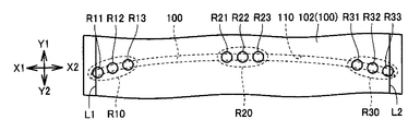
- measurement apparatus 11 includes position information on region R10 on one end side of processing line 110, position information on region R20 near the center of processing line 110, and region on the other end side of processing line 110. R30 position information was measured.
- the region R10 is near the region where the alignment line L1 formed near the end on the arrow X1 direction side on the substrate 100 and the processing line 110 intersect.
- the region R30 is near the region where the alignment line L2 formed near the end on the arrow X2 direction side on the substrate 100 and the processing line 110 intersect.
- the measuring device 11 measured position information of three locations (positions R11, R12, R13) as position information of the region R10.
- the measuring device 11 measured position information of three locations (positions R21, R22, R23) as position information of the region R20.
- the measuring device 11 measured position information at three locations (positions R31, R32, R33) as position information of the region R30.
- Three points are measured at each of the measurement positions R10, R20, and R30, and are acquired as multi-point data in preparation for a recognition error (reading error) due to scratches or dirt on the glass substrate that is the substrate 100. Further, it is preferable to read three or more points to determine whether the acquired data is an abnormal value.
- a second harmonic YVO4 laser was processed on the photoelectric conversion layer 102 through the glass surface.
- a plurality of processing lines 120 (contact lines) were formed on the photoelectric conversion layer 102 so as to be arranged substantially in parallel with an interval (P1) of about 120 ⁇ m.
- P1 an interval of about 120 ⁇ m.
- the back electrode layer 103 was formed to cover the photoelectric conversion layer 102 and the plurality of processing lines 120.
- the back electrode layer 103 was formed by sequentially laminating ZnO and Ag at a temperature of about 140 ° C. using a magnetron sputtering method.
- the position information of the processing line 120 was measured. Based on the positional information on the processing line 120, the second tide wave YVO4 laser was processed on the back electrode layer 103 through the glass surface. A plurality of processing lines 130 (separation lines) were formed on the back electrode layer 103 so as to be arranged substantially in parallel with a spacing (P2) of about 120 ⁇ m. When the temperature of the substrate 100 at this time was measured, the highest value was about 28 ° C. (equal to room temperature).
- the processing line 110, the processing line 120, and the processing line 130 are formed without overlapping each other.
- the processing line 110, the processing line 120, and the processing line 130 are formed without overlapping each other. It was proved that a thin film solar cell can be obtained.
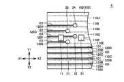
- the laser processing apparatus 4 includes adjacent laser heads 31 to 34.
- the positions of the laser heads 31 to 34 can be controlled independently by the control device.
- the laser heads 31 and 32 are arranged at an interval TY31 on the arrow Y1 direction side.
- the laser heads 32 and 33 are arranged at an interval TY32 on the arrow Y1 direction side.
- the laser heads 33 and 34 are arranged on the arrow Y1 direction side with an interval TY33.
- the intervals TY31, TY32, and TY33 are preferably substantially the same as the interval (RY11) on the arrow Y1 direction side of each processing line 110A to 110J.
- the measuring apparatus 11 is arranged on the arrow X1 direction (one side) of the laser head 32.
- the measuring device 21 is disposed on the arrow X2 direction (the other side) of the laser head 32.
- the substrate 100 is prepared.
- a transparent conductive film 101 is formed on the substrate 100.
- processing lines 110A to 110J extending along the directions of the arrows X1 and X2 are formed on the transparent conductive film 101.
- the photoelectric conversion layer 102 is formed so as to cover the transparent conductive film 101 and the processing lines 110A to 110J.
- the substrate 100 over which the photoelectric conversion layer 102 is formed moves to the arrow X2 direction side.
- the measuring device 11 measures the position information of the processing line 110B on the arrow X1 direction side from the laser heads 31-34.
- the position information of the processing line 110B is input to the control device 80 through the image processing unit 88 (FIG. 1).
- the laser heads 31 to 34 emit laser light.
- the laser light processes the photoelectric conversion layer 102 located above the processing lines 110A to 110D.
- the control device 80 (FIG. 1) controls the irradiation position of the laser beam based on the position information of the processing line 110B.
- the control device 80 controls the irradiation position of the laser beam so that the processing line 120A does not overlap with the processing line 110A.
- the control device 80 controls the irradiation position of the laser beam so that the interval between the processing line 120A and the processing line 110A is as narrow as possible (as designed).
- control device 80 controls the irradiation position of the laser beam so that the processing lines 120B to 120D do not overlap with the processing lines 110B to 110D, respectively.
- the control device 80 controls the irradiation position of the laser beam so that the intervals between the processing lines 120B to 120D and the processing lines 110B to 110D are as narrow as possible (as designed values).
- processing lines 120A to 120D extending along the directions of the arrows X1 and X2 are formed on the photoelectric conversion layer 102.
- the measuring devices 11 and 21 move in the direction of the arrow Y1 until they reach the side of the processing line 110F.
- the laser head 31 moves to the arrow Y1 direction side until it reaches the side of the processing line 110E.
- the laser heads 32 to 34 move in the direction of the arrow Y1 until they reach the sides of the processing lines 110F to 110H, respectively.
- the laser heads 31 to 34 and the measuring devices 11 and 21 may move in the direction of the arrow Y1 until they reach the sides of the other four processing lines.
- the laser heads 31 to 34 emit laser light.
- the laser beam processes the photoelectric conversion layer 102 located above the processing lines 110E to 110H.
- the control device 80 (FIG. 1) controls the irradiation position of the laser beam based on the position information of the processing line 110F.
- the control device 80 controls the irradiation position of the laser beam so that the processing lines 120E to 120H are not formed overlapping the processing lines 110E to 110H, respectively.
- the control device 80 controls the irradiation position of the laser beam so that the distance between the processing lines 120E to 120H and the processing lines 110E to 110H is as narrow as possible (as designed).
- Process lines 120E to 120H extending along the arrow X1 and X2 directions are formed on the photoelectric conversion layer 102.
- the laser heads 31 to 34 and the measuring apparatuses 11 and 21 repeat the above operation for other processing lines. As described above, the thin film solar cell according to the present embodiment is obtained.
- the integration interval P of general solar cells 108 is about 5 mm to 15 mm.
- the interval between the processing lines 110A to 110D is also about 5 mm to about 15 mm. Since the interval is small, the temperature difference of the photoelectric conversion layer 102 (or the transparent conductive film 101) in the vicinity of the processing lines 110A to 110D is small. Even if the processing lines 110A to 110D are curved, the processing lines 110A to 110D draw substantially similar trajectories.
- the processing lines 120A to 120D are formed based on the position information of the processing line 110B, the processing lines 120A to 120D are formed without overlapping the processing lines 110A to 110D formed below the processing lines 120A to 120D. .
- the processing lines 120A to 120D are formed so that the distance from the processing lines 110A to 110D formed below the processing lines 120A to 120D is as narrow as possible (as designed).
- the measuring devices 11 and 21 are arranged in the same straight line as the laser head 32 (arrow X1, X2 direction side), the measuring device 21 may be arranged on the arrow X1, X2 direction side of the adjacent laser head 33.
- There is no restriction on the number of laser heads there are four laser heads close to each other, and there may be a plurality of units.
- a method of providing a close beam such as a method of spiriting a beam with an optical system using a diffraction grating, may be realized by means already known.
- the laser processing apparatus 4 compared with the laser processing apparatus 1 in the first embodiment and the laser processing apparatus 2 in the second embodiment, when the number of beams is the same, the number of measuring apparatuses can be reduced, and the equipment cost is reduced. Can be suppressed.
- An interval TY11 on the arrow Y1 direction side between the center 31C of the laser head 31 and the center 11C of the measuring device 11 is set in advance as an offset amount with respect to the center 31C of the laser head 31 of the control device 80 (FIG. 1). It is good to leave.
- An interval TX11 on the arrow X1 direction side between the center 31C of the laser head 31 and the center 11C of the measuring device 11 may be set in advance as an offset amount with respect to the center 31C of the laser head 31 of the control device 80.
- the interval TY21 on the arrow Y1 direction side between the center 31C of the laser head 31 and the center 21C of the measuring device 21 may be set in advance as an offset amount with respect to the control device 80 (FIG. 1).
- An interval TX21 on the arrow X1 direction side between the center 31C of the laser head 31 and the center 21C of the measuring device 21 may be set in advance as an offset amount with respect to the control device 80.
- the center 32C of the irradiation image 32F in the laser head 32, the center 33C of the irradiation image 33F in the laser head 33, and the center 34C of the irradiation image 34F in the laser head 34 are offset amounts with respect to the control device 80. It is good to set in advance.
- the laser processing apparatus 4 may include a correcting unit 89.
- the substrate 100 may be fixed, and the laser heads 31 to 34 and the measuring devices 11 and 21 may be moved in the directions of the arrows X1, X2, Y1, and Y2. .
- the measuring devices 11 and 21 may be movable together with the laser heads 31 to 34 with respect to the substrate 100, or may be movable integrally with the laser heads 31 to 34.
- the laser heads 31 to 34 and the measuring devices 11 and 21 may be relatively movable, and may be configured to be separately controlled in position.
- the laser heads 31 to 34 and the measuring devices 11 and 21 may be configured so that the positions of the laser heads 31 to 34 and the measuring devices 11 and 21 can be finely adjusted regardless of whether they move together or separately.
- the laser processing device 4 may form a processing line for the photoelectric conversion layer and the back electrode layer.
- the measuring devices 11 and 21 may measure position information of the processing line 110B (or processing line 110C) located closest to the center on the arrow Y1 direction side among the processing lines 110A to 110D. Higher processing accuracy can be obtained.
- the aspect of forming the processing line (120) along the processing lines 110A to 110D and the processing lines 110E to 110H that are adjacent to each other has been described.
- the present invention can also be implemented in such a manner that the processing lines (120) are formed for the processing lines (110) that are not adjacent to each other.
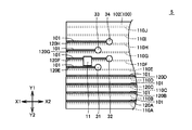
- the laser processing device 5 includes a measuring device 11.
- the laser processing device 5 does not include the measuring device 21 (see FIG. 19).
- the measuring device 11 is disposed on the arrow X1 direction (one side) of the laser head 32.
- the substrate 100 is prepared.
- a transparent conductive film 101 is formed on the substrate 100.
- processing lines 110A to 110J extending along the directions of the arrows X1 and X2 are formed on the transparent conductive film 101.
- the photoelectric conversion layer 102 is formed so as to cover the transparent conductive film 101 and the processing lines 110A to 110J.
- the substrate 100 on which the photoelectric conversion layer 102 is formed moves to the arrow X2 direction side.
- the measuring device 11 measures the position information of the processing line 110B on the arrow X1 direction side from the laser heads 31-34.
- the position information of the processing line 110B is input to the control device 80 through the image processing unit 88 (FIG. 1).
- the control device 80 controls the irradiation position of the laser beam based on the position information of the processing line 110B.
- process lines 120A to 120D extending along arrow X1 and X2 directions are formed on the photoelectric conversion layer 102.
- the measuring device 11 moves to the arrow Y1 direction side until reaching the side of the processing line 110F.
- the laser head 31 moves to the arrow Y1 direction side until it reaches the side of the processing line 110E.
- the laser heads 32 to 34 move in the direction of the arrow Y1 until they reach the sides of the processing lines 110F to 110H, respectively.
- the control device 80 uses the positional information of the processing line 110B (measured when the measuring device 11 is scanning in the direction of the arrow X1). Based on this, the irradiation position of the laser beam is controlled.
- the processing lines 120E to 120H extending along the arrow X1 and X2 directions are formed on the photoelectric conversion layer 102.
- the laser heads 31 to 34 and the measuring device 11 repeat the above operation for other processing lines. As described above, the thin film solar cell according to the present embodiment is obtained.
- the integration interval P of general solar cells 108 is about 5 mm to 15 mm.
- the intervals between the processing lines 110A to 110H are also about 5 mm to about 15 mm. Since the interval is small, the temperature difference of the photoelectric conversion layer 102 (or the transparent conductive film 101) in the vicinity of the processing lines 110A to 110H is small. Even if the processing lines 110A to 110H are curved, the processing lines 110A to 110H draw substantially similar trajectories.
- the processing lines 120E to 120H are formed based on the position information of the processing line 110B, the processing lines 120E to 120H are formed without overlapping the processing lines 110E to 110H formed below the processing lines 120E to 120H. .
- the processing lines 120E to 120H are formed so that the distance from the processing lines 110E to 110H formed below the processing lines 120E to 120H is as narrow as possible (as designed).
- the number of measuring apparatuses can be reduced as compared with the laser processing apparatus 4 in the above-described fourth embodiment, so that the equipment cost can be reduced.
- the processing tact can be improved because the moving distance in the direction of the arrows X 1 and X 2 is shorter than that of the laser processing device 4.
- the apparatus size in the direction of the arrows X1 and X2 can be made compact and the footprint can be reduced.
- the interval TY11 on the arrow Y1 direction side between the center 31C of the laser head 31 and the center 11C of the measuring device 11 may be set in advance as an offset amount for the control device 80.
- An interval TX11 on the arrow X1 direction side between the center 31C of the laser head 31 and the center 11C of the measuring device 11 may be set in advance as an offset amount with respect to the control device 80 (FIG. 1).
- the center 32C of the irradiation image 32F in the laser head 32, the center 33C of the irradiation image 33F in the laser head 33, and the center 34C of the irradiation image 34F in the laser head 34 are offset amounts with respect to the control device 80. It is good to set in advance.
- the laser processing apparatus 5 may include a correcting unit 89.
- the substrate 100 may be fixed and the laser heads 31 to 34 and the measuring device 11 may be configured to be movable in the directions of the arrows X1, X2, Y1, and Y2. Good.
- the measuring device 11 may be movable together with the laser heads 31 to 34 with respect to the substrate 100, or may be movable integrally with the laser heads 31 to 34.
- the laser heads 31 to 34 and the measuring device 11 may be relatively movable, or may be configured to be separately controlled in position.
- the laser heads 31 to 34 and the measuring device 11 may be configured so that the positions of the laser heads 31 to 34 and the measuring device 11 can be finely adjusted regardless of whether they move together or separately.
- the laser processing apparatus in this embodiment may form a processing line for the photoelectric conversion layer and the back electrode layer.
- the measuring device 11 may measure position information of the processing line 110B (or processing line 110C) positioned closest to the center on the arrow Y1 direction side among the processing lines 110A to 110D. It is possible to obtain an average value of information on a plurality of machining positions and obtain high machining accuracy.
- the machining line (120) is machined along the machining lines 110A to 110D and the machining lines 110E to 110H that are adjacent to each other has been described.
- the invention can also be implemented in such a manner that the processing lines (120) are formed for the processing lines (110) that are not adjacent to each other.
- the laser processing device 6 includes a measuring device 11.
- the laser processing device 6 does not include the measuring device 21 (see FIG. 19).
- the measuring apparatus 11 is arranged on the arrow Y1 direction side of the laser heads 31 to 34.
- the distance TY11 between the laser head 32 and the measuring apparatus 11 on the arrow Y1 direction side may be substantially the same as four times the distance (RY11) on the arrow Y1 direction side of each processing line 110A to 110J (interval RY41).
- the substrate 100 is prepared.
- a transparent conductive film 101 is formed on the substrate 100.
- processing lines 110A to 110J extending along the directions of the arrows X1 and X2 are formed on the transparent conductive film 101.
- the photoelectric conversion layer 102 is formed so as to cover the transparent conductive film 101 and the processing lines 110A to 110J.
- the substrate 100 on which the photoelectric conversion layer 102 is formed moves to the arrow X2 direction side.
- the substrate 100 passes below the measuring device 11.
- the measuring device 11 scans the photoelectric conversion layer 102 in the arrow X1 direction side.
- the measuring device 11 measures position information of the processing line 110B.
- the position information of the processing line 110B is input to the control device 80 through the image processing unit 88 (FIG. 1).
- the measuring device 11 moves to the arrow Y1 direction side until it reaches the side of the processing line 110F.
- the laser head 31 moves to the arrow Y1 direction side until reaching the side of the processing line 110A.
- the laser heads 32 to 34 move in the direction of the arrow Y1 until they reach the sides of the processing lines 110B to 110D, respectively.
- the control device 80 uses the positional information of the processing line 110B (measured when the measuring device 11 is scanning in the direction of the arrow X1). Based on this, the irradiation position of the laser beam is controlled. In this way, processing lines 120A to 120D extending along the arrow X1 and X2 directions are formed on the photoelectric conversion layer 102.
- the measuring device 11 scans the photoelectric conversion layer 102 in the direction of the arrow X2.
- the measuring device 11 measures position information of the processing line 110F.
- the measuring device 11 moves to the arrow Y1 direction side until reaching the side of the processing line 110J.
- the laser head 31 moves to the arrow Y1 direction side until it reaches the side of the processing line 110E.
- the laser heads 32 to 34 move in the direction of the arrow Y1 until they reach the sides of the processing lines 110F to 110H, respectively.
- the laser heads 31 to 34 repeat the same operation as described above for other processing lines.
- the measuring device 11 repeats the above operation for other processing lines.
- the thin film solar cell according to the present embodiment is obtained.
- the number of measuring apparatuses can be reduced as compared with the control apparatus in the fourth embodiment, so that the equipment cost can be reduced.
- the movement distance on the arrow X1, X2 side is smaller, so the size on the arrow X1, X2 side can be reduced (arrow Y1).
- Y2 side is increased by the pitch, but the effect of reducing the size of the arrows X1 and X2 is greater), and the apparatus can be made compact and the equipment cost can be reduced.
- the interval TY11 on the arrow Y1 direction side between the center 31C of the laser head 31 and the center 11C of the measuring device 11 may be set in advance as an offset amount for the control device 80.
- An interval TX11 on the arrow X1 direction side between the center 31C of the laser head 31 and the center 11C of the measuring device 11 may be set in advance as an offset amount with respect to the control device 80 (FIG. 1).
- the center 32C of the irradiation image 32F in the laser head 32, the center 33C of the irradiation image 33F in the laser head 33, and the center 34C of the irradiation image 34F in the laser head 34 are offset amounts with respect to the control device 80. It is good to set in advance.
- the laser processing apparatus 6 may include a correcting unit 89.
- the substrate 100 may be fixed, and the laser heads 31 to 34 and the measuring device 11 may be moved in the directions of the arrows X1, X2, Y1, and Y2.
- the measuring device 11 may be movable together with the laser heads 31 to 34 with respect to the substrate 100, or may be movable integrally with the laser heads 31 to 34.
- the laser heads 31 to 34 and the measuring device 11 may be relatively movable, or may be configured to be separately controlled in position.
- the laser heads 31 to 34 and the measuring device 11 may be configured so that the positions of the laser heads 31 to 34 and the measuring device 11 can be finely adjusted regardless of whether they move together or separately.
- the laser processing apparatus 6 may form a processing line for the photoelectric conversion layer and the back electrode layer.
- the measuring device 11 may measure position information of the processing line 110B (or processing line 110C) positioned closest to the center on the arrow Y1 direction side among the processing lines 110A to 110D. It is possible to obtain an average value of information on a plurality of machining positions and obtain high machining accuracy.
- the processing line (120) is formed along the processing lines 110A to 110D and the processing lines 110E to 110H that are adjacent to each other.
- the present invention can also be implemented in such a manner that the processing lines (120) are formed for the processing lines (110) that are not adjacent to each other.
- the laser processing device 7 includes a laser head 31, a laser processing device 87, a measuring device 24, a transport device 90, a fiber 81, a laser oscillator 86, a control device 80, and an image processing unit 88.
- the laser oscillated from the laser oscillator 86 is transmitted to the laser head 31 through the fiber 81.
- the laser oscillated from the laser oscillator 86 may be transmitted to the laser head 31 by a so-called spatial transmission method.
- the laser is emitted from the laser head 31 (downward in the drawing).
- the laser is, for example, a YAG laser or a YVO4 laser.
- the substrate 100 is placed on the transfer device 90.
- the transfer device 90 may include support pins (not shown) and the like in order to adjust the flatness of the substrate 100.
- the substrate 100 is fixed at a predetermined position by a predetermined fixing member (not shown).
- the transfer device 90 moves the substrate 100 to the arrow X1 direction side.
- the substrate 100 passes through the inlet portion 92, the inside 93, and the outlet portion 94 of the laser processing apparatus 87 in the arrow X1 direction side.
- the measuring device 24 is arranged on the side of the entrance portion 92 in the direction of the arrow X2.
- the measuring device 24 is disposed above the transport device 90.
- the measuring device 24 includes imaging means such as a camera.
- the resolution of the imaging means is preferably 20 ⁇ m or less.
- the resolution of the imaging means is 10 ⁇ m or less.
- the laser head 31 is supported above the conveying device 90 in the inside 93 of the laser processing device 87.
- the laser head 31 is movable in the directions of arrows Y1 and Y2.
- the substrate 100 is prepared.
- a transparent conductive film 101 is formed on the surface of the substrate 100.
- a plurality of processing lines 110 (first processing lines) arranged substantially in parallel toward the arrow Y1 direction are formed.
- a photoelectric conversion layer 102 is formed so as to cover the transparent conductive film 101 and the processing line 110.
- the substrate 100 is placed on the transfer device 90 (on the entrance 92 side).
- the substrate 100 moves to the arrow X1 direction side.
- the substrate 100 passes under the measuring device 24.
- the measuring device 24 obtains information for the photoelectric conversion layer 102 with respect to the arrow X2 direction side.
- the measuring device 24 measures position information of the processing line 110.
- the position information measured by the measuring device 24 is input to the control device 80 through the image processing unit 88.
- the substrate 100 moves to the inside 93 of the laser processing apparatus 87.
- the substrate 100 passes below the laser head 31.
- the laser head 31 irradiates the laser.
- the laser beam processes the photoelectric conversion layer 102 located above the processing line 110.
- the control device 80 controls the irradiation position of the laser light based on the position information of the processing line 110.
- the irradiation position of the laser beam is controlled by moving the laser head 31 in the directions of the arrows Y1 and Y2.
- the control device 80 controls the irradiation position of the laser beam so that the processing line 120 does not overlap with the processing line 110.
- the control device 80 controls the irradiation position of the laser beam so that the interval between the processing line 120 and the processing line 110 is as narrow as possible (as designed). In this way, the processing line 120 extending along the arrow X1 and X2 directions is formed on the photoelectric conversion layer 102.
- the processing line 120 can be continuously formed on the plurality of substrates 100 (the upper photoelectric conversion layer 102) by including the transfer device 90. Regardless of the apparatus configuration in the laser apparatus, it is possible to adapt to all apparatuses.
- the laser processing apparatus 7a which concerns on the modification of Embodiment 7 is demonstrated.
- the laser processing apparatus 7a may further include a correcting unit 89.
- measurement apparatus 24 (FIG. 29) adds position information of end surface 100T of substrate 100, position information of alignment line L1, and position of alignment line L2. Information is measured.
- each position information measured by the measurement device 24 (a portion indicated by a solid line in FIG. 31) and a position where the substrate 100 is actually disposed (a portion indicated by a dotted line in FIG. 31). May not match (displace).
- the position where the substrate 100 is actually arranged is indicated by a processing line 110z, an end face 100Tz, an alignment line L1z, and an alignment line L2z.
- the correction means 89 suppresses the deviation that occurs as described above. Specifically, the correction unit 89 calculates the difference between the inclination of the processing line 110 in the XY plane (hereinafter referred to as inclination) measured by the measuring device 24 and the actual processing line 110z.
- the inclination of the processing line 110 is calculated by (coordinate A1-coordinate A2).
- the inclination of the processing line 110z is calculated by (coordinate A1z ⁇ coordinate A2z).
- the correcting unit 89 calculates the difference between the inclination of the end face 100T measured by the measuring device 24 and the actual inclination of the end face 100Tz.
- the correcting unit 89 calculates the difference between the inclination of the alignment line L1 measured by the measuring device 24 and the actual inclination of the alignment line L1z.
- the correcting unit 89 calculates the difference between the inclination of the alignment line L2 measured by the measuring device 24 and the actual inclination of the alignment line L2z.
- the correction unit 89 inputs the difference between the four inclinations calculated as described above to the control device 80 as an offset amount. Based on the offset amount, the control device 80 corrects the irradiation position of the laser beam. Since the laser processing apparatus 7a further includes the correction unit 89, it is possible to form a processing line with higher accuracy.
Landscapes
- Laser Beam Processing (AREA)
- Photovoltaic Devices (AREA)
Abstract
レーザ加工装置(1)は、レーザヘッド(31)、測定装置(11,21)および制御装置(80)を備える。レーザヘッド(31)の、一方側に測定装置(11)が、他方側に測定装置(21)が配置される。基板(100)上の第2層に対して、レーザヘッド(31)が一方側に移動するとき、測定装置(11)はレーザヘッド(31)の移動方向前方において第1加工ラインの位置情報を測定し、レーザヘッド(31)が他方側に移動するとき、測定装置(21)はレーザヘッド(31)の移動方向前方において第1加工ラインの位置情報を測定する。制御装置(80)が上記位置情報に基づきレーザ光の照射位置を制御する。第1加工ラインに沿う第2加工ラインが第2層上に形成される。レーザ加工装置(1)によれば、基板上に形成される複数の層のそれぞれに、製造効率を落とさずに複数の加工ラインが所定の間隔で且つ相互に重ならずに形成される。
Description
この発明は、基板上に形成される複数の層のそれぞれに、複数の加工ラインが形成される薄膜太陽電池、その製造方法、および薄膜太陽電池製造用のレーザ加工装置に関する。
図32を参照して、一般的な薄膜太陽電池1000の製造方法について説明する。基板100上に、透明導電膜101が成膜される。透明導電膜101にレーザ光を照射することにより、透明導電膜101上に複数の加工ライン110(分離ラインとも称される)が形成される。透明導電膜101および加工ライン110を覆うように、光電変換層102が成膜される。光電変換層102にレーザ光を照射することにより、光電変換層102上に複数の加工ライン120(コンタクトラインとも称される)が形成される。
光電変換層102および加工ライン120を覆うように、裏面電極層103が成膜される。裏面電極層103にレーザ光を照射することにより、裏面電極層103上に複数の加工ライン130(分離ラインとも称される)が形成される。基板100上に、直列接続された複数の太陽電池セル108が形成される。太陽電池セル108の集積間隔Pは、約5mm~約15mmである。上記同様の製造方法が、特開2007-48835号公報(特許文献1)に開示されている。
加工ライン110,120,130を(平面視において)含む領域W1は、発電に寄与しない。領域W1を小さくするためには、加工ライン110と加工ライン120との間隔P1、または、加工ライン120と加工ライン130との間隔P2を狭くする必要がある。間隔P1,P2を狭くするためには、レーザ光が、所望の位置に高い精度で照射される必要がある。
本発明者は、上述の技術について検討を行い、以下のような課題またはその源泉を見出した。図33を参照して、光電変換層(102)または裏面電極層(103)は、基板100上に高い温度で成膜される。基板100に光電変換層102が成膜された後の経過時間と、基板100上の任意の位置PL1~PL5における温度変化(室温環境)との関係を測定した。基板100として、ガラス基板(1000mm×1400mm×4mm)を使用した。
図34を参照して(一例:自然冷却)、成膜完了直後(0分)においては、位置PL1~PL5に温度差は生じていない。成膜完了後、すぐに(約1~2分後)、基板100の外周側(位置PL1,PL5)と、基板100の中央側(位置PL2~PL4)との間に温度差が生じる。成膜完了後約30分が経過しても、基板100の外周側(位置PL1,PL5)と、基板100の中央側(位置PL2~PL4)との間には、約20℃の温度差が生じている。
図35を参照して、光電変換層102は、透明導電膜101上に高い温度で成膜される。基板100の外周側と、基板100の中央側との間には、上記同様の温度差が生じる。当該温度差により、基板100の外周側と、基板100の中央側との間において、熱膨張の程度に差が生じる。その結果、透明導電膜101上に形成された複数の加工ライン110は、所定の時間、湾曲する。同様に、裏面電極層103も高い温度で成膜されるため、光電変換層102上に形成された複数の加工ライン120は、所定の時間、湾曲する。
図36を参照して、当該湾曲により、加工ライン120が加工ライン110に重なって形成される場合がある。加工ライン120と加工ライン110とが重なると、薄膜太陽電池1000の特性が低下したり、電気的な接続の不良が発生したりする(加工ライン120と加工ライン130についても同様である)。加工ライン120と加工ライン110とが重なることを抑制するために、基板100の温度が低くなる(加工ライン110の湾曲が回復する)のを待つことも不可能ではないが、時間を要するため製造効率が低下する。これに対し、光電変換層102は薄膜太陽電池の特性に影響を与える重要な層であり、光電変換層102の形成後に短時間で次の工程を行なうことが極めて重要となる。
本発明は、基板上に形成される複数の層のそれぞれに、製造効率を落とさずに複数の加工ラインが所定の間隔で且つ相互に重ならずに形成される薄膜太陽電池、その製造方法、および薄膜太陽電池製造用のレーザ加工装置を提供することを目的とする。
本発明の第1の局面に基づく薄膜太陽電池製造用のレーザ加工装置は、基板上の第1層に並べて形成された複数の第1加工ラインに沿うように、上記第1層の上方に積層された第2層に第2加工ラインを形成する薄膜太陽電池製造用のレーザ加工装置であって、ステージと、レーザ光を照射し、上記ステージに載置された上記基板に対して一方側および他方側に向かって相対的に移動可能なレーザヘッドと、上記レーザヘッドの上記一方側に配置され、上記レーザヘッドとともに上記基板に対して相対的に移動可能な第1測定装置と、上記レーザヘッドの上記他方側に配置され、上記レーザヘッドとともに上記基板に対して相対的に移動可能な第2測定装置と、制御装置と、を備え、上記レーザヘッドが上記一方側に向かって移動するとき、上記第1測定装置は、上記レーザヘッドの移動方向前方において第1の上記第1加工ラインの位置情報を測定し、上記制御装置は、第1の上記第2加工ラインが第1の上記第1加工ラインに沿って形成されるように、第1の上記第1加工ラインの上記位置情報に基づいて上記レーザ光の照射位置を制御し、上記レーザヘッドが上記他方側に向かって移動するとき、上記第2測定装置は、上記レーザヘッドの移動方向前方において第2の上記第1加工ラインの上記位置情報を測定し、上記制御装置は、第2の上記第2加工ラインが第2の上記第1加工ラインに沿って形成されるように、第2の上記第1加工ラインの上記位置情報に基づいて上記レーザ光の上記照射位置を制御する。
本発明の第2の局面に基づく薄膜太陽電池製造用のレーザ加工装置は、基板上の第1層に並べて形成された複数の第1加工ラインに沿うように、上記第1層の上方に積層された第2層に第2加工ラインを形成する薄膜太陽電池製造用のレーザ加工装置であって、ステージと、レーザ光を照射し、上記ステージに載置された上記基板に対して一方側および他方側に向かって相対的に移動可能なレーザヘッドと、上記レーザヘッドの上記一方側に配置され、上記レーザヘッドとともに上記基板に対して相対的に移動可能な測定装置と、制御装置と、を備え、上記レーザヘッドが上記一方側に向かって移動するとき、上記測定装置は、上記レーザヘッドの移動方向前方において第1の上記第1加工ラインの位置情報を測定し、上記制御装置は、第1の上記第2加工ラインが第1の上記第1加工ラインに沿って形成されるように、第1の上記第1加工ラインの上記位置情報に基づいて上記レーザ光の照射位置を制御し、上記レーザヘッドが上記他方側に向かって移動するとき、上記制御装置は、第2の上記第2加工ラインが第2の上記第1加工ラインに沿って形成されるように、第1の上記第1加工ラインの上記位置情報に基づいて上記レーザ光の上記照射位置を制御する。
本発明の第3の局面に基づく薄膜太陽電池製造用のレーザ加工装置は、基板上の第1層に並べて形成された複数の第1加工ラインに沿うように、上記第1層の上方に積層された第2層に第2加工ラインを形成する薄膜太陽電池製造用のレーザ加工装置であって、ステージと、レーザ光を照射し、上記ステージに載置された上記基板に対して一方側および他方側に向かって相対的に移動可能なレーザヘッドと、上記レーザヘッドの上記第1加工ラインが並ぶ方向側に配置され、上記レーザヘッドとともに上記基板に対して相対的に移動可能な測定装置と、制御装置と、を備え、上記レーザヘッドが上記一方側または上記他方側に向かって移動しながら上記レーザ光を照射して第1の上記第1加工ラインに沿って上記第2加工ラインを形成するとき、上記測定装置は、上記レーザヘッドの上記第1加工ラインが並ぶ方向側に位置する第2の上記第1加工ラインの位置情報を測定し、上記レーザヘッドが上記一方側または上記他方側に向かって移動するとき、上記制御装置は、上記第2加工ラインが第2の上記第1加工ラインに沿って形成されるように、第2の上記第1加工ラインの上記位置情報に基づいて上記レーザ光の照射位置を制御する。
本発明の第4の局面に基づく薄膜太陽電池の製造方法は、基板上の第1層に対してレーザ光を走査することにより第1加工ラインを形成する第1工程と、上記第1層および上記第1加工ラインの上方に第2層を形成する第2工程と、上記第2層に対して所定の方向側に向かって上記レーザ光を走査するとともに、該レーザ光の走査方向前方において上記第1加工ラインの位置情報を測定し、上記第2層に第2加工ラインが上記第1加工ラインに沿って形成されるように、上記位置情報に基づいて上記レーザ光の照射位置を制御する第3工程と、を備える。
本発明の第5の局面に基づく薄膜太陽電池の製造方法は、基板上の第1層に対してレーザ光を走査することにより複数並ぶように形成された第1加工ラインと、上記第1層および上記第1加工ラインの上方に形成された第2層と、を有する積層体を準備する第1工程と、上記第2層に対して一方側に向かって上記レーザ光を走査しながら上記第2層に該レーザ光を照射するとともに、該レーザ光の走査方向前方において第1の上記第1加工ラインの位置情報を測定し、上記第2層に第1の第2加工ラインが第1の上記第1加工ラインに沿って形成されるように、第1の上記第1加工ラインの上記位置情報に基づいて上記レーザ光の照射位置を制御する第2工程と、上記第2層に対して他方側に向かって上記レーザ光を走査しながら上記第2層に該レーザ光を照射するとともに、上記第2層に第2の第2加工ラインが第2の上記第1加工ラインに沿って形成されるように、上記第2工程において測定した第1の上記第1加工ラインの上記位置情報に基づいて上記レーザ光の上記照射位置を制御する第3工程と、を備える。
本発明の第6の局面に基づく薄膜太陽電池の製造方法は、基板上の第1層に対してレーザ光を走査することにより複数並ぶように形成された第1加工ラインと、上記第1層および上記第1加工ラインの上方に形成された第2層と、を有する積層体を準備する第1工程と、上記第2層に対して上記レーザ光を走査しながら上記第2層に該レーザ光を照射し、第1の上記第1加工ラインに沿って上記第2層に第1の第2加工ラインを形成するとともに、第2の上記第1加工ラインの位置情報を測定する第2工程と、第2の上記第1加工ラインの上記位置情報に基づいて上記レーザ光の照射位置を制御して上記第2層に対して上記レーザ光を走査し、第2の上記第1加工ラインに沿って上記第2層に第2の第2加工ラインを形成する第3工程と、を備える。
本発明の第7の局面に基づく薄膜太陽電池の製造方法は、基板上の第1層に形成された第1加工ラインに沿うように、第2加工ラインを上記第1層の上方に積層された第2層に形成する薄膜太陽電池の製造方法であって、上記第1加工ラインの位置情報を、レーザ加工装置の外部において測定する第1工程と、上記基板を上記レーザ加工装置に対して相対的に移動させ、上記基板を上記レーザ加工装置の内部に配置させる第2工程と、上記第2層に対してレーザ光を走査するとともに、上記第2層に上記第2加工ラインが上記第1加工ラインに沿って形成されるように、上記位置情報に基づいて上記レーザ光の照射位置を制御する第3工程と、を備える。
本発明の第8の局面に基づく薄膜太陽電池は、上記第1の局面に基づく薄膜太陽電池製造用のレーザ加工装置を使用して製造される。
本発明の第9の局面に基づく薄膜太陽電池は、上記第4の局面に基づく薄膜太陽電池の製造方法を使用して製造される。
本発明によれば、基板上に形成される複数の層のそれぞれに、製造効率を落とさずに複数の加工ラインが所定の間隔で且つ相互に重ならずに形成される薄膜太陽電池、その製造方法、および薄膜太陽電池製造用のレーザ加工装置を得ることができる。
本発明に基づいた各実施の形態における薄膜太陽電池、薄膜太陽電池の製造方法および薄膜太陽電池製造用のレーザ加工装置(以下、単にレーザ加工装置と称する場合がある)について、以下、図面を参照しながら説明する。各実施の形態の説明において、個数、量などに言及する場合、特に記載がある場合を除き、本発明の範囲は必ずしもその個数、量などに限定されない。各実施の形態の説明において、同一の部品、相当部品に対しては、同一の参照番号を付し、重複する説明は繰り返さない場合がある。
[実施の形態1]
(レーザ加工装置1の構成)
図1~図3を参照して、本実施の形態における薄膜太陽電池製造用のレーザ加工装置1について説明する。図1を参照して、レーザ加工装置1は、レーザヘッド31,32、測定装置11(第1測定装置),測定装置21(第2測定装置),測定装置12,22、ヘッド駆動機構71,72、ヘッド支持装置75、ファイバ81,82、レーザ発振器86、制御装置80、画像処理ユニット88、ベース70、ステージ駆動部74、ステージ76、および固定部材78を備えている。
(レーザ加工装置1の構成)
図1~図3を参照して、本実施の形態における薄膜太陽電池製造用のレーザ加工装置1について説明する。図1を参照して、レーザ加工装置1は、レーザヘッド31,32、測定装置11(第1測定装置),測定装置21(第2測定装置),測定装置12,22、ヘッド駆動機構71,72、ヘッド支持装置75、ファイバ81,82、レーザ発振器86、制御装置80、画像処理ユニット88、ベース70、ステージ駆動部74、ステージ76、および固定部材78を備えている。
レーザ発振器86から発振されたレーザは、ファイバ81を通ってレーザヘッド31に伝送される。レーザ発振器86から発振されたレーザは、いわゆる空間伝送方式によりレーザヘッド31に伝送されてもよい。レーザは、レーザヘッド31から(紙面垂直方向の紙面奥行き側に向かって)出射される。レーザとは、YAGレーザまたはYVO4レーザ等である。
測定装置11は、レーザヘッド31の一方側として、たとえば矢印X1方向側に配置されている。測定装置21は、レーザヘッド31の他方側として、たとえば矢印X2方向側に配置されている。測定装置11,21は、カメラ等の撮像手段を含んでいる。
レーザヘッド31および測定装置11,21は、ヘッド支持装置75により上方(紙面垂直方向の紙面手前側)から支持されている。ヘッド駆動機構71は、レーザヘッド31および測定装置11,21を、矢印Y1方向側および矢印Y2方向側に移動させる。
ファイバ82、レーザヘッド32、測定装置12,22、およびヘッド駆動機構72は、ファイバ81、レーザヘッド31、測定装置11,21、およびヘッド駆動機構71と同様に構成される。
ステージ76上には、基板100が載置される。ステージ76は、基板100の平面度を調節するために、支持ピン(不図示)など備えているとよい。基板100は、固定部材78により所定の位置に固定される。ステージ駆動部74は、ステージ76を、矢印X1方向側および矢印X2方向側に移動させる。ステージ駆動部74により、基板100は、レーザヘッド31,32の下方、測定装置11,21,12,22の下方を、矢印X1方向側および矢印X2方向側に移動可能である。
(レーザ加工装置1による薄膜太陽電池の製造方法)
まず、基板100が準備される。基板100は、絶縁性および透光性を有するガラス基板等である。基板100は、矢印X2方向側に移動する。熱CVD法またはスパッタ法等により、基板100上に透明導電膜101(第1層)(図32参照)が成膜される。透明導電膜101は、SnO2、ITO、またはZnO等である。
まず、基板100が準備される。基板100は、絶縁性および透光性を有するガラス基板等である。基板100は、矢印X2方向側に移動する。熱CVD法またはスパッタ法等により、基板100上に透明導電膜101(第1層)(図32参照)が成膜される。透明導電膜101は、SnO2、ITO、またはZnO等である。
基板100は、レーザ光を照射しているレーザヘッド31,32の下方を通過する。レーザ光は、透明導電膜101に対して加工を行なう。透明導電膜に、矢印X1,X2方向側に沿って延びる加工ライン110(図32参照)が形成される。
基板100がレーザヘッド31,32の下方を矢印X1方向側に通過した後、レーザヘッド31,32は、矢印Y1方向側に所定の距離だけ移動する。基板100は、矢印X2方向側に移動する。基板100は、レーザ光を照射しているレーザヘッド31,32の下方を通過する。透明導電膜101上に、矢印X1,X2方向側に沿って延びる他の加工ライン110が形成される。この際、透明導電膜101の加工ライン110の形成に用いる装置としては、測定装置11、21、12および22を省いてもかまわない。
基板100およびレーザヘッド31,32は、上記の動作を複数回繰り返す。透明導電膜101に、矢印X1,X2方向側に沿って延びる複数の加工ライン110が、矢印Y1方向側に向かって略平行に並んで形成される。
透明導電膜101および複数の加工ライン110を覆うように、プラズマCVD法等により、光電変換層102(第2層)(図32参照)を成膜する。光電変換層102は、順次積層されたp層、i層およびn層により構成される。
(矢印X2方向側)
図2を参照して、光電変換層102が成膜された基板100は、矢印X2方向側に移動する。基板100は、測定装置11の下方を通過する。測定装置11は、光電変換層102に対して矢印X1方向側に走査する。測定装置11は、レーザヘッド31よりも矢印X1方向側において、加工ライン110A(第1の第1加工ライン)の位置情報を測定する。
図2を参照して、光電変換層102が成膜された基板100は、矢印X2方向側に移動する。基板100は、測定装置11の下方を通過する。測定装置11は、光電変換層102に対して矢印X1方向側に走査する。測定装置11は、レーザヘッド31よりも矢印X1方向側において、加工ライン110A(第1の第1加工ライン)の位置情報を測定する。
測定装置11は、処理速度または情報量等の観点から、加工ライン110A上の位置情報を間欠的(部分的)に測定するとよい。たとえば、測定装置11は、基板100の大きさが1000mm×1400mmである場合、加工ライン110A上の3箇所以上、または5箇所以上の位置情報を測定するとよい。求める加工精度(設計値)に合わせて、測定ポイント数を選択するとよい。加工ライン110Aの位置情報は、画像処理ユニット88(図1)を通して、制御装置80に入力される。
基板100が矢印X2方向側に移動するとき、レーザヘッド31はレーザ光を照射している。レーザ光は、加工ライン110Aに沿うように光電変換層102に対して加工を行なう。レーザ光が光電変換層102に対して加工を行なうとき、制御装置80(図1)は、加工ライン110Aの位置情報に基づいて、レーザ光の照射位置を制御する。
制御装置80は、加工ライン120Aが加工ライン110Aと重なって形成されないように、レーザ光の照射位置を制御する。制御装置80は、加工ライン120Aと加工ライン110Aとの間隔が極力狭くなるように(設計値通りに)、レーザ光の照射位置を制御する。制御装置80は、レーザヘッド31を矢印Y1方向側または矢印Y2方向側に移動させることにより、レーザ光の照射位置を制御する。こうして、矢印X1,X2方向側に沿って延びる加工ライン120A(第1の第2加工ライン)が、光電変換層102に形成される。
測定装置11が加工ライン110Aの位置情報を測定した後すぐに、レーザ光の照射位置は制御されるとよい。換言すると、測定装置11が加工ライン110Aの位置情報を測定する工程と、レーザ光の照射位置が制御される工程とは、別々の工程であったとしても、可能な限り短い時間の間(略同一の工程)に行なわれるとよい。
レーザヘッド32および測定装置21は、レーザヘッド31および測定装置11と同様に動作する。レーザヘッド32および測定装置11により、矢印X1,X2方向側に沿って延びる加工ライン120Fが形成される。
加工ライン120A,120Fが形成された後、レーザヘッド31および測定装置11,21は、加工ライン110Bの側方に到達するまで、矢印Y1方向側に移動する。レーザヘッド32および測定装置12,22は、加工ライン110Gの側方に到達するまで、矢印Y1方向側に移動する。
(矢印X1方向側)
図3を参照して、加工ライン120A,120Fが形成された基板100は、矢印X1方向側に移動する。基板100は、測定装置21の下方を通過する。測定装置21は、光電変換層102に対して矢印X2方向側に走査する。測定装置21は、レーザヘッド31よりも矢印X2方向側において、加工ライン110B(第2の第1加工ライン)の位置情報を測定する。加工ライン110Bの位置情報は、画像処理ユニット88(図1)を通して、制御装置80に入力される。
図3を参照して、加工ライン120A,120Fが形成された基板100は、矢印X1方向側に移動する。基板100は、測定装置21の下方を通過する。測定装置21は、光電変換層102に対して矢印X2方向側に走査する。測定装置21は、レーザヘッド31よりも矢印X2方向側において、加工ライン110B(第2の第1加工ライン)の位置情報を測定する。加工ライン110Bの位置情報は、画像処理ユニット88(図1)を通して、制御装置80に入力される。
基板100が矢印X1方向側に移動するとき、レーザヘッド31はレーザ光を照射している。レーザ光は、加工ライン110Bに沿うように光電変換層102に対して加工を行なう。レーザ光が光電変換層102に対して加工を行なうとき、制御装置80(図1)は、加工ライン110Bの位置情報に基づいてレーザ光の照射位置を制御する。
制御装置80は、加工ライン120Bが加工ライン110Bと重なって形成されないように、レーザ光の照射位置を制御する。制御装置80は、加工ライン120Bと加工ライン110Bとの間隔が極力狭くなるように(設計値通りに)、レーザ光の照射位置を制御する。制御装置80は、レーザヘッド31を矢印Y1方向側または矢印Y2方向側に移動させることにより、レーザ光の照射位置を制御する。こうして、矢印X1,X2方向側に沿って延びる加工ライン120B(第2の第2加工ライン)が、光電変換層102上に形成される。
測定装置21が加工ライン110Bの位置情報を測定した後すぐに、レーザ光の照射位置は制御されるとよい。換言すると、測定装置21が加工ライン110Bの位置情報を測定する工程と、レーザ光の照射位置が制御される工程とは、別々の工程であったとしても、可能な限り短い時間の間(略同一の工程)において行なわれるとよい。
レーザヘッド32および測定装置22は、レーザヘッド31および測定装置21と同様に動作する。レーザヘッド32および測定装置22により、矢印X1,X2方向側に沿って延びる加工ライン120Gが形成される。
レーザヘッド31および測定装置11,21は、上記の動作を加工ライン110C~110Eに対して繰り返す。レーザヘッド32および測定装置12,22は、上記の動作を加工ライン110H~110Jに対して繰り返す。以上のようにして、本実施の形態に係る薄膜太陽電池が得られる。
第2加工ライン120が形成された後、光電変換層102上および第2加工ライン120上に裏面電極層103が形成される。裏面電極層103は、たとえばスパッタ法や真空蒸着法等の方法により、ZnO、ITOまたはSnO2等の透明電極層と、AgまたはAL等の金属層とを積層することにより形成される。裏面電極層103は、約100nm~約500nmの厚さにするとよい。
次に、裏面電極層103に第3加工ラインを形成する。第3加工ラインは、上述した第2加工ラインと同様の方法により形成することができる。第3加工ライン形成においては、第1加工ラインまたは第2加工ラインの何れを位置情報の測定の対象としてもよい。
加工ラインとしては、第1加工ライン、第2加工ラインおよび第3加工ラインがこの順に略平行に並べて形成される。この構成により、第1から第3加工ラインを間に介して隣接する一方の太陽電池セルの透明導電膜101と他方の裏面電極層103とを電気的に接続することができ、複数の太陽電池セルが直列接続された集積型の薄膜太陽電池が得られる。
なお、本実施の形態1および以降の他のすべての実施の形態を含む本願発明において、「第1の第1加工ラインに沿って第2加工ラインを形成する」とは、第1の第1加工ラインに近接した位置に第2加工ラインを形成する場合に限らず、第1の第1加工ラインから離れた位置に第2加工ラインを形成する場合も含まれる。たとえば、第1の第1加工ラインと並んで形成された、第1の第1加工ライン側から数えて数本目(望ましくは2本目)までのうちの何れかの第1加工ライン(第2の第1加工ライン)に近接する位置に第2加工ラインを形成する場合も含まれる。ここで、第1の第1加工ラインと第2加工ラインとの相対的な加工位置精度向上のためには、第1の第1加工ラインと隣り合う第1加工ラインを第2の第1加工ラインとし、該ラインに近接するように第2加工ラインを形成することが望ましく、第1の第1加工ラインに近接するように第2加工ラインを形成することがさらに望ましい。
(効果)
基板100が矢印X2方向側に移動するとき、測定装置11が動作する。基板100が矢印X1方向側に移動するとき、測定装置21が動作する。基板100の移動方向に応じて測定装置11,21が動作する。レーザ加工装置1によれば、迅速に加工ラインを形成することができる。
基板100が矢印X2方向側に移動するとき、測定装置11が動作する。基板100が矢印X1方向側に移動するとき、測定装置21が動作する。基板100の移動方向に応じて測定装置11,21が動作する。レーザ加工装置1によれば、迅速に加工ラインを形成することができる。
レーザ加工装置1によれば、光電変換層上の加工ラインは、透明導電膜上の加工ラインと重なることなく形成される。光電変換層上の加工ラインは、透明導電膜上の加工ラインとの間隔が極力狭くなるように(設計値通りに)形成される。
[実施の形態1の他の形態]
(実施の形態1の第1変形例)
図4を参照して、実施の形態1の第1変形例に係るレーザ加工装置1aについて説明する。レーザヘッド31からレーザ光が照射されることにより、被照射物(透明導電膜等)上に照射像31Fが形成される。照射像31Fは、中心31Cを有している。測定装置11は、被照射物上において撮像範囲11Fを有している。撮像範囲11Fは、中心11Cを有している。測定装置21は、被照射物上において撮像範囲21Fを有している。測定装置21は、中心21Cを有している。
(実施の形態1の第1変形例)
図4を参照して、実施の形態1の第1変形例に係るレーザ加工装置1aについて説明する。レーザヘッド31からレーザ光が照射されることにより、被照射物(透明導電膜等)上に照射像31Fが形成される。照射像31Fは、中心31Cを有している。測定装置11は、被照射物上において撮像範囲11Fを有している。撮像範囲11Fは、中心11Cを有している。測定装置21は、被照射物上において撮像範囲21Fを有している。測定装置21は、中心21Cを有している。
レーザ加工装置1aにおいては、照射像31Fの中心31Cと、撮像範囲11Fの中心11Cと、撮像範囲21Fの中心21Cとは、同一の直線D1上に配置されているとよい。この場合、当該直線D1と、基板100の移動方向(矢印X1方向側または矢印X2方向側)とが平行になるように、レーザヘッド31および測定装置11,21が配置されているとよい。レーザ加工装置1aは、より精度の高い加工ラインを形成することが可能となる。
照射像31Fの中心31Cと、撮像範囲11Fの中心11Cと、撮像範囲21Fの中心21Cとを同一の直線D1上に配置することが物理的に困難である場合もある。この場合、制御装置80に対し、各中心11C,21C,31Cの位置と、上記直線D1との間隔を、オフセット量として予め設定しておくとよい。
(実施の形態1の第2変形例)
図1を参照して、実施の形態1の第2変形例に係るレーザ加工装置1bについて説明する。レーザ加工装置1bは、補正手段89をさらに備えているとよい。レーザ加工装置1bを長時間使用していると、レーザヘッド31と、測定装置11,21との相対的な位置関係にずれが生じる場合がある。レーザ加工装置1bが設置されている環境の温度変化等により、測定装置11,21との相対的な位置関係にずれが生じる場合もある。
図1を参照して、実施の形態1の第2変形例に係るレーザ加工装置1bについて説明する。レーザ加工装置1bは、補正手段89をさらに備えているとよい。レーザ加工装置1bを長時間使用していると、レーザヘッド31と、測定装置11,21との相対的な位置関係にずれが生じる場合がある。レーザ加工装置1bが設置されている環境の温度変化等により、測定装置11,21との相対的な位置関係にずれが生じる場合もある。
図5を参照して、具体的に説明する。レーザ加工装置1bの起動時には、レーザヘッド31の中心31Cと、測定装置11の中心11Cとの間には、矢印X1,X2方向側に、所定の間隔LXが設定されている。レーザヘッド31の中心31Cと、測定装置11の中心11Cとの間には、矢印Y1,Y2方向側に、所定の間隔LY(=0)が設定されている(レーザヘッド31の中心31Cと、測定装置11の中心11Cとは、略同一の直線D1上に配置されている)。
図6を参照して、所定の外部要因により、上記間隔LX(図5)は、間隔LX+αに変化する。上記間隔LY(図5)は、間隔LY+βに変化する。これらの変化により、形成される加工ラインの位置も変化する。
図7を参照して、たとえば、上記間隔LY(図5)が、間隔LY+β(図6)に変化したとする。この場合、光電変換層102上に実際に形成された加工ライン120は、本来、光電変換層102上に形成されるべき所望の加工ライン120Xの位置に対し、矢印Y1方向側に距離βの分だけずれて形成される。
補正手段89は、上記のように生じるずれを抑制する。具体的には、補正手段89は、測定装置11から、実際に形成された加工ライン120の矢印Y1方向側におけるエッジ部(または中心部)の位置情報を取得する。補正手段89は、取得した位置情報と、本来、光電変換層102上に形成されるべき所望の加工ライン120Xの位置情報とを対比する。たとえば、加工ライン110と所望の加工ライン110Xの中心間の距離と実際に形成された加工ライン110との中心間の距離との差(=距離β)とを対比する。
補正手段89は、取得した位置情報と、本来、光電変換層102上に形成されるべき所望の加工ライン120Xの位置情報とが一致していない場合、制御装置80に対し、その差分をオフセット量として設定する。当該オフセット量に基づき、制御装置80はレーザ光の照射位置を補正する。当該補正は、加工精度の観点からは、1つの加工ラインが形成される毎に行なわれるとよい。当該補正は、製造時間の観点からは、1つの基板(100)を製造する毎に行なわれてもよい。
(非発電領域106上における補正)
図8を参照して、レーザ加工装置1bにおける基板100の周縁部には、非発電領域106が形成されている。基板100の中央部には、発電領域104が形成されている。補正手段89は、非発電領域106において、レーザ光の照射位置を補正してもよい。非発電領域106の幅は、約5mm~約15mmである。
図8を参照して、レーザ加工装置1bにおける基板100の周縁部には、非発電領域106が形成されている。基板100の中央部には、発電領域104が形成されている。補正手段89は、非発電領域106において、レーザ光の照射位置を補正してもよい。非発電領域106の幅は、約5mm~約15mmである。
より具体的に説明する。補正手段89は、測定装置11(図1)から、絶縁エリアを確保する為の非発電領域106上における所定の基準点51の位置情報を取得する。補正手段89は、基準点51(任意の位置に設定可能)の位置情報を制御装置80(図1)に入力する。制御装置80は、基準点51の位置情報に基づいて、レーザヘッド31(図1)から照射されるレーザ光の照射位置を制御する。レーザ光は、基準点51に向かって照射される。
補正手段89は、測定装置11から取得した基準点51の位置情報と、形成された加工ライン(点)の実際の位置情報とを対比する。補正手段89は、測定装置11から取得した基準点51の位置情報と、形成された加工ライン(点)の実際の位置情報とが一致していない場合、制御装置80に対し、その差分をオフセット量として入力する。当該オフセット量に基づき、制御装置80はレーザ光の照射位置を補正する。
(ダミー基板200上における補正)
図8を参照して、レーザ加工装置1bは、ダミー基板200をさらに備えていてもよい。補正手段89は、測定装置11(図1)から、ダミー基板200上における所定の基準点52の位置情報を取得する。補正手段89は、基準点52の位置情報を制御装置80(図1)に入力する。制御装置80は、基準点52(任意の位置に設定可能)の位置情報に基づいて、レーザヘッド31(図1)から照射されるレーザ光の照射位置を制御する。レーザ光は、基準点52に向かって照射される。
図8を参照して、レーザ加工装置1bは、ダミー基板200をさらに備えていてもよい。補正手段89は、測定装置11(図1)から、ダミー基板200上における所定の基準点52の位置情報を取得する。補正手段89は、基準点52の位置情報を制御装置80(図1)に入力する。制御装置80は、基準点52(任意の位置に設定可能)の位置情報に基づいて、レーザヘッド31(図1)から照射されるレーザ光の照射位置を制御する。レーザ光は、基準点52に向かって照射される。
補正手段89は、測定装置11から取得した基準点52の位置情報と、形成された加工ライン(点)の実際の位置情報とを対比する。補正手段89は、測定装置11から取得した基準点52の位置情報と、形成された加工ライン(点)の実際の位置情報とが一致していない場合、制御装置80に対し、その差分をオフセット量として入力する。当該オフセット量に基づき、制御装置80はレーザ光の照射位置を補正する。
補正するタイミングとして、装置稼動を考慮して、1日1回程度であることが好ましい。ただし、たとえば、前工程からの基板の受け入れが無い状態が生じれば、受け入れの最終基板に対して、その都度補正を行えば良いことになる。さらに、位置ずれ補正のデータ取得を複数回行えば、より安定して精度をあげることができる。
レーザ加工装置1bは、補正手段89をさらに備えていることにより、より精度の高い加工ラインを安定して形成することが可能となる。
(実施の形態1のその他の変形例)
図1を参照して、上述の実施の形態1においては、基板100を矢印X1,X2方向側に移動させる態様に基づいて説明した。基板100を固定し、レーザヘッド31,32および測定装置11,21,12,22を、矢印X1,X2,Y1,Y2方向側に移動させてもよい。測定装置11,21は、基板100に対して、レーザヘッド31とともに移動可能であってもよく、レーザヘッド31と一体的に移動可能であってもよい。レーザヘッド31と測定装置11,21とは相対的に移動可能であってもよく、別々に位置制御されるように構成されてもよい。レーザヘッド31と測定装置11,21とは、一体的に移動する場合であっても、別々に移動する場合であっても、それぞれの位置を微調整可能に構成するとよい。これらはすべて、測定装置12,22とレーザヘッド32との関係においても同様である。
図1を参照して、上述の実施の形態1においては、基板100を矢印X1,X2方向側に移動させる態様に基づいて説明した。基板100を固定し、レーザヘッド31,32および測定装置11,21,12,22を、矢印X1,X2,Y1,Y2方向側に移動させてもよい。測定装置11,21は、基板100に対して、レーザヘッド31とともに移動可能であってもよく、レーザヘッド31と一体的に移動可能であってもよい。レーザヘッド31と測定装置11,21とは相対的に移動可能であってもよく、別々に位置制御されるように構成されてもよい。レーザヘッド31と測定装置11,21とは、一体的に移動する場合であっても、別々に移動する場合であっても、それぞれの位置を微調整可能に構成するとよい。これらはすべて、測定装置12,22とレーザヘッド32との関係においても同様である。
上述の実施の形態1においては、レーザヘッド31およびレーザヘッド32からレーザがそれぞれ出射される場合について説明しているが、いずれか1つであってもよい。また、レーザヘッドが3つ以上にて構成されても構わない。
上述の実施の形態1においては、レーザ加工装置1が、透明導電膜101の加工軌跡に対して光電変換層102の加工ラインを形成するという態様に基づいて説明した。レーザ加工装置1は、光電変換層102(第1層に相当する)の加工軌跡に対して、裏面電極層103(第2層に相当する)の加工ラインを形成してもよいし、透明導電膜101の軌跡に対して、裏面電極層103(第2層に相当する)の加工ラインを形成してもよい。裏面電極層103は、たとえばZnO、ITOまたはSnO2等の透明導電層と、AgまたはAL等の金属層とを積層することにより構成される。裏面電極層は、約100nm~約500nmの厚さにするとよい。
[実施の形態2]
図9および図10を参照して、本実施の形態における薄膜太陽電池のレーザ加工装置2について説明する。ここでは、上述の実施の形態1におけるレーザ加工装置1との相違点についてのみ説明する。
図9および図10を参照して、本実施の形態における薄膜太陽電池のレーザ加工装置2について説明する。ここでは、上述の実施の形態1におけるレーザ加工装置1との相違点についてのみ説明する。
図9を参照して、レーザ加工装置2は、測定装置11および測定装置12を備えている。レーザ加工装置2は、測定装置21,22(図2参照)を備えていない。測定装置11は、レーザヘッド31の矢印X1方向(一方)側に配置されている。測定装置12は、レーザヘッド32の矢印X1方向側に配置されている。
(レーザ加工装置2による薄膜太陽電池の製造方法)
上述の実施の形態1と同様に、まず、基板100が準備される。基板100上に透明導電膜101が成膜される。レーザヘッド31,32により、透明導電膜101上に、矢印X1,X2方向側に沿って延びる加工ライン110A~110Jが形成される。透明導電膜101および加工ライン110A~110Jを覆うように、光電変換層102が成膜される。
上述の実施の形態1と同様に、まず、基板100が準備される。基板100上に透明導電膜101が成膜される。レーザヘッド31,32により、透明導電膜101上に、矢印X1,X2方向側に沿って延びる加工ライン110A~110Jが形成される。透明導電膜101および加工ライン110A~110Jを覆うように、光電変換層102が成膜される。
(矢印X2方向側)
実施の形態1と同様に、光電変換層102が成膜された基板100は、矢印X2方向側に移動する。測定装置11は、レーザヘッド31よりも矢印X1方向側において、加工ライン110A(第1の第1加工ライン)の位置情報を測定する。加工ライン110Aの位置情報は、画像処理ユニット88(図1)を通して、制御装置80に入力される。
実施の形態1と同様に、光電変換層102が成膜された基板100は、矢印X2方向側に移動する。測定装置11は、レーザヘッド31よりも矢印X1方向側において、加工ライン110A(第1の第1加工ライン)の位置情報を測定する。加工ライン110Aの位置情報は、画像処理ユニット88(図1)を通して、制御装置80に入力される。
制御装置80は、加工ライン120Aが加工ライン110Aと重なって形成されないように、レーザ光の照射位置を制御する。制御装置80は、加工ライン120Aと加工ライン110Aとの間隔が極力狭くなるように(設計値通りに)、レーザ光の照射位置を制御する。こうして、矢印X1,X2方向側に沿って延びる加工ライン120A(第1の第2加工ライン)が、光電変換層102上に形成される。
レーザヘッド32および測定装置12は、レーザヘッド31および測定装置11と同様に動作する。レーザヘッド32および測定装置12により、矢印X1,X2方向側に沿って延びる加工ライン120Fが形成される。
加工ライン120A,120Fが形成された後、レーザヘッド31および測定装置11は、(加工ライン110Aに隣り合う)加工ライン110Bの側方に到達するまで、矢印Y1方向側に移動する。レーザヘッド32および測定装置12は、(加工ライン110Fに隣り合う)加工ライン110Gの側方に到達するまで、矢印Y1方向側に移動する。
(矢印X1方向側)
図10を参照して、加工ライン120A,120Fが形成された基板100は、矢印X1方向側に移動する。基板100が矢印X1方向側に移動するとき、レーザヘッド31はレーザ光を照射している。レーザ光は、加工ライン110Bの上方に位置する光電変換層102に対して加工を行なう。
図10を参照して、加工ライン120A,120Fが形成された基板100は、矢印X1方向側に移動する。基板100が矢印X1方向側に移動するとき、レーザヘッド31はレーザ光を照射している。レーザ光は、加工ライン110Bの上方に位置する光電変換層102に対して加工を行なう。
レーザ光が光電変換層102に対して加工を行なうとき、制御装置80(図1)は、(測定装置11が矢印X1方向側に走査しているときに測定した)加工ライン110Aの位置情報に基づいて、レーザ光の照射位置を制御する。こうして、矢印X1,X2方向側に沿って延びる加工ライン120B(第2の第2加工ライン)が、光電変換層102に形成される。
レーザヘッド32および測定装置12は、レーザヘッド31および測定装置11と同様に動作する。レーザヘッド32および測定装置11により、矢印X1,X2方向側に沿って延びる加工ライン120Gが形成される。
レーザヘッド31および測定装置11は、上記の動作を加工ライン110C~110Eに対して繰り返す。レーザヘッド32および測定装置12は、上記の動作を加工ライン110H~110Jに対して繰り返す。以上のようにして、本実施の形態に係る薄膜太陽電池が得られる。
上記の実施の形態2においては、第1の第1加工ライン(例えば110A)について測定された位置情報に基づいて、第1の第1加工ラインと隣り合う第2の第1加工ライン(例えば110B)に近接する位置に第2加工ライン(例えば120B)を形成したが、第2の第1加工ライン(例えば110C)に近接する位置に第2加工ライン(例えば120C)を形成する場合、第2の第1加工ライン(110C)と隣り合わない第1の第1加工ライン(110A)について測定された位置情報に基づいて、上記第2加工ライン(120C)を形成することも可能である。なお、第2加工ラインと第1の第1加工ラインの相対的な位置精度の観点から、第2加工ラインが近接して形成される第2の第1加工ラインと、第2加工ラインを形成する際に参照される位置情報が測定された第1の第1加工ラインとの間に存在する第1加工ラインは、1本以下であることが望ましい。
(効果)
冒頭の説明のとおり、一般的な太陽電池セル108(図32参照)の集積間隔Pは、約5mm~15mmである。加工ライン110Aと、(加工ライン110Aに隣り合う)加工ライン110Bとの間隔も、約5mm~約15mmである。当該間隔が小さいため、加工ライン110A付近における光電変換層102(または透明導電膜101)と、加工ライン110B付近における光電変換層102(または透明導電膜101)との分布は近い。加工ライン110A,110Bが湾曲していたとしても、加工ライン110A,110Bは略同様の軌跡を描く。
冒頭の説明のとおり、一般的な太陽電池セル108(図32参照)の集積間隔Pは、約5mm~15mmである。加工ライン110Aと、(加工ライン110Aに隣り合う)加工ライン110Bとの間隔も、約5mm~約15mmである。当該間隔が小さいため、加工ライン110A付近における光電変換層102(または透明導電膜101)と、加工ライン110B付近における光電変換層102(または透明導電膜101)との分布は近い。加工ライン110A,110Bが湾曲していたとしても、加工ライン110A,110Bは略同様の軌跡を描く。
加工ライン110Aの位置情報に基づいて加工ライン120Bを形成したとしても、加工ライン120Bは、加工ライン120Bの下方に形成された加工ライン110Bと重なることなく形成される。加工ライン120Bは、加工ライン110Bとの間隔が極力狭くなるように(設計値通りに)形成される。
レーザ加工装置2によれば、上述の実施の形態1におけるレーザ加工装置1に比べて測定装置の数が少なくてすむので設備費用を削減できる。レーザ加工装置2によれば、レーザ加工装置1に比べて矢印X1,X2方向側の移動距離が少ない分、処理タクトを向上させることができ、矢印X1,X2方向側の装置サイズをコンパクトにできフットプリントを小さくできる。
[実施の形態2の変形例]
図11を参照して、実施の形態2の変形例に係るレーザ加工装置2aについて説明する。実施の形態1の第1変形例と同様に、レーザヘッド31の中心31Cと、測定装置11の中心11Cとは、同一の直線D1上に配置されているとよい。この場合、当該直線D1と、基板100の移動方向(矢印X1方向側または矢印X2方向側)とが平行になるように、レーザヘッド31および測定装置11が配置されているとよい。レーザ加工装置2aは、より精度の高い加工ラインを形成することが可能となる。
図11を参照して、実施の形態2の変形例に係るレーザ加工装置2aについて説明する。実施の形態1の第1変形例と同様に、レーザヘッド31の中心31Cと、測定装置11の中心11Cとは、同一の直線D1上に配置されているとよい。この場合、当該直線D1と、基板100の移動方向(矢印X1方向側または矢印X2方向側)とが平行になるように、レーザヘッド31および測定装置11が配置されているとよい。レーザ加工装置2aは、より精度の高い加工ラインを形成することが可能となる。
レーザヘッド31の中心31Cと、測定装置11の中心11Cとを同一の直線D1上に配置することが物理的に困難である場合もある。この場合、制御装置80に対し、各中心11C,31Cの位置と、上記直線D1との間隔を、オフセット量として予め設定しておくとよい。
(実施の形態2のその他の変形例)
上述の実施の形態1の第2変形例と同様に、レーザ加工装置2は、補正手段89を備えているとよい。上述の実施の形態1のその他の変形例と同様に、基板100を固定し、レーザヘッド31,32および測定装置11,12を、矢印X1,X2,Y1,Y2方向側に移動させてもよい。
上述の実施の形態1の第2変形例と同様に、レーザ加工装置2は、補正手段89を備えているとよい。上述の実施の形態1のその他の変形例と同様に、基板100を固定し、レーザヘッド31,32および測定装置11,12を、矢印X1,X2,Y1,Y2方向側に移動させてもよい。
測定装置11は、基板100に対して、レーザヘッド31とともに移動可能であってもよく、レーザヘッド31と一体的に移動可能であってもよい。レーザヘッド31と測定装置11とは相対的に移動可能であってもよく、別々に位置制御されるように構成されてもよい。レーザヘッド31と測定装置11とは、一体的に移動する場合であっても、別々に移動する場合であっても、それぞれの位置を微調整可能に構成するとよい。これらはすべて、測定装置12とレーザヘッド32との関係においても同様である。
レーザヘッド31およびレーザヘッド32は、いずれか1つであってもよいし、レーザヘッドが3つ以上にて構成されても構わない。レーザ加工装置2は、光電変換層および裏面電極層に対して加工ラインを形成してもよい。
[実施の形態3]
図12および図13を参照して、本実施の形態における薄膜太陽電池のレーザ加工装置3について説明する。ここでは、上述の実施の形態1におけるレーザ加工装置1との相違点についてのみ説明する。
図12および図13を参照して、本実施の形態における薄膜太陽電池のレーザ加工装置3について説明する。ここでは、上述の実施の形態1におけるレーザ加工装置1との相違点についてのみ説明する。
図12を参照して、レーザ加工装置3は、測定装置11および測定装置12を備えている。測定装置11は、レーザヘッド31の矢印Y1方向側に配置されている。
測定装置11と、レーザヘッド31との矢印Y1方向側の間隔TY11は、各加工ライン110A~110Jの矢印Y1方向側の間隔(RY11)と略同一であることが好ましい。測定装置12およびレーザヘッド32は、測定装置11およびレーザヘッド31と同様に構成される。
(レーザ加工装置3による薄膜太陽電池の製造方法)
上述の実施の形態1と同様に、まず、基板100が準備される。基板100上に透明導電膜101が成膜される。レーザヘッド31,32により、透明導電膜101に、矢印X1,X2方向側に沿って延びる加工ライン110A~110Jが形成される。透明導電膜101および加工ライン110A~110Jを覆うように、光電変換層102が成膜される。
上述の実施の形態1と同様に、まず、基板100が準備される。基板100上に透明導電膜101が成膜される。レーザヘッド31,32により、透明導電膜101に、矢印X1,X2方向側に沿って延びる加工ライン110A~110Jが形成される。透明導電膜101および加工ライン110A~110Jを覆うように、光電変換層102が成膜される。
(矢印X2方向側)
光電変換層102が成膜された基板100は、矢印X2方向側に移動する。基板100は、測定装置11の下方を通過する。測定装置11は、光電変換層102に対して矢印X1方向側に対する位置情報を入手する。測定装置11は、加工ライン110A(第1の第1加工ライン)の位置情報を測定する。加工ライン110Aの位置情報は、画像処理ユニット88(図1)を通して制御装置80に入力される。
光電変換層102が成膜された基板100は、矢印X2方向側に移動する。基板100は、測定装置11の下方を通過する。測定装置11は、光電変換層102に対して矢印X1方向側に対する位置情報を入手する。測定装置11は、加工ライン110A(第1の第1加工ライン)の位置情報を測定する。加工ライン110Aの位置情報は、画像処理ユニット88(図1)を通して制御装置80に入力される。
測定装置12は、測定装置11と同様に動作する。測定装置11は、加工ライン110Fの位置情報を測定する。
基板100が測定装置11の下方を通過した後、レーザヘッド31は、加工ライン110Aの側方に到達するまで、矢印Y1方向側に移動する。測定装置11は、(加工ライン110Aに隣り合う)加工ライン110B(第2の第1加工ライン)の側方に到達するまで、矢印Y1方向側に移動する。
同様に、レーザヘッド32は、加工ライン110Fの側方に到達するまで、矢印Y1方向側に移動する。測定装置12は、加工ライン110Gの側方に到達するまで、矢印Y1方向側に移動する。
(矢印X1方向側)
図13を参照して、基板100は、矢印X1方向側に移動する。基板100が矢印X1方向側に移動するとき、レーザヘッド31はレーザ光を照射している。レーザ光は、加工ライン110Aに沿うように光電変換層102に対して加工を行なう。
図13を参照して、基板100は、矢印X1方向側に移動する。基板100が矢印X1方向側に移動するとき、レーザヘッド31はレーザ光を照射している。レーザ光は、加工ライン110Aに沿うように光電変換層102に対して加工を行なう。
レーザ光が光電変換層102に対して加工を行なうとき、制御装置80(図1)は、(測定装置11が矢印X1方向側に走査しているときに測定した)加工ライン110Aの位置情報に基づいて、レーザ光の照射位置を制御する。こうして、矢印X1,X2方向側に沿って延びる加工ライン120A(第1の第2加工ライン)が、光電変換層102に形成される。
基板100が矢印X1方向側に移動するとき、測定装置11は、光電変換層102に対して矢印X2方向側に対する位置情報を入手する。測定装置11は、加工ライン110B(第2の第1加工ライン)の位置情報を測定する。
レーザヘッド32および測定装置12は、レーザヘッド31および測定装置11と同様に動作する。レーザヘッド32により、矢印X1,X2方向側に沿って延びる加工ライン120Fが形成される。測定装置12は、加工ライン110Gの位置情報を測定する。
加工ライン120A,120Fが形成された後、レーザヘッド31は、加工ライン110Bの側方に到達するまで、矢印Y1方向側に移動する。測定装置11は、加工ライン110Cの側方に到達するまで、矢印Y1方向側に移動する。
同様に、レーザヘッド32は、加工ライン110Gの側方に到達するまで、矢印Y1方向側に移動する。測定装置12は、加工ライン110Hの側方に到達するまで、矢印Y1方向側に移動する。
(矢印X2方向側)
図14を参照して、基板100は、矢印X2方向側に移動する。レーザヘッド31,32および測定装置11,12は、上記同様に動作する。
図14を参照して、基板100は、矢印X2方向側に移動する。レーザヘッド31,32および測定装置11,12は、上記同様に動作する。
レーザヘッド31は、上記同様の動作を加工ライン110C~110Eに対して繰り返す。測定装置11は、上記の動作を加工ライン110D,110Eに対して繰り返す。レーザヘッド32は、上記同様の動作を加工ライン110H~110Jに対して繰り返す。測定装置12は、上記の動作を加工ライン110I,110Jに対して繰り返す。以上のようにして、本実施の形態に係る薄膜太陽電池が得られる。
上記の実施の形態3においては、第1の第1加工ライン(例えば110A)について測定された位置情報に基づいて、第1の第1加工ライン(110A)に近接する位置に第2加工ライン(120A)を形成したが、第1の第1加工ライン(110A)と異なる第2の第1加工ライン(例えば110C)について測定された位置情報に基づいて、上記第2加工ライン(120A)を形成することも可能である。なお、第2加工ラインと第1の第1加工ラインの相対的な位置精度の観点から、第2加工ラインが近接して形成される第1の第1加工ラインと、第2加工ラインを形成する際に参照される位置情報が測定された第2の第1加工ラインとの間に存在する第1加工ラインは、1本以下であることが望ましい。
(効果)
レーザ加工装置3によれば、上述の実施の形態1におけるレーザ加工装置1および実施の形態2におけるレーザ加工装置2に比べて、矢印X1,X2側の移動距離が少ない分、矢印X1,X2側のサイズを小さくでき(矢印Y1,Y2側はピッチ分大きくなるが、矢印X1,X2側のサイズの小さくできる効果の方が大きい)、装置をコンパクトにすることができ設備コストを低減できる。また、データを取得するのにも時間的な余裕があり、データ処理が容易となる。実施の形態1におけるレーザ加工装置1と比べると、測定装置の数が少なくてすみ、設備コストを少なくできる。
レーザ加工装置3によれば、上述の実施の形態1におけるレーザ加工装置1および実施の形態2におけるレーザ加工装置2に比べて、矢印X1,X2側の移動距離が少ない分、矢印X1,X2側のサイズを小さくでき(矢印Y1,Y2側はピッチ分大きくなるが、矢印X1,X2側のサイズの小さくできる効果の方が大きい)、装置をコンパクトにすることができ設備コストを低減できる。また、データを取得するのにも時間的な余裕があり、データ処理が容易となる。実施の形態1におけるレーザ加工装置1と比べると、測定装置の数が少なくてすみ、設備コストを少なくできる。
[実施の形態3の変形例]
図15を参照して、実施の形態3の変形例に係るレーザ加工装置3aについて説明する。レーザヘッド31の中心31Cと、測定装置11の中心11Cとは、略同一の直線D1上に配置されているとよい。
図15を参照して、実施の形態3の変形例に係るレーザ加工装置3aについて説明する。レーザヘッド31の中心31Cと、測定装置11の中心11Cとは、略同一の直線D1上に配置されているとよい。
レーザヘッド31の中心31Cと、測定装置11の中心11Cとを同一の直線D1上に配置することが物理的に困難である場合もある。この場合、制御装置80に対し、各中心11C,31Cの位置と、上記直線D1との間隔を、オフセット量として予め設定しておくとよい。
(実施の形態3のその他の変形例)
図12を参照して、レーザ加工装置3は、レーザヘッド31と測定装置11との間隔TY11が調節可能なように構成されているとよい。集積間隔P(図32参照)が異なる太陽電池セル108を製造することにも、柔軟に対応することができる。
図12を参照して、レーザ加工装置3は、レーザヘッド31と測定装置11との間隔TY11が調節可能なように構成されているとよい。集積間隔P(図32参照)が異なる太陽電池セル108を製造することにも、柔軟に対応することができる。
上述の実施の形態1の第2変形例と同様に、レーザ加工装置3は、補正手段89を備えているとよい。上述の実施の形態1のその他の変形例と同様に、基板100を固定し、レーザヘッド31,32および測定装置11,12を、矢印X1,X2,Y1,Y2方向側に移動させてもよい。測定装置11は、基板100に対して、レーザヘッド31とともに移動可能であってもよく、レーザヘッド31と一体的に移動可能であってもよい。レーザヘッド31と測定装置11とは相対的に移動可能であってもよく、別々に位置制御されるように構成されてもよい。レーザヘッド31と測定装置11とは、一体的に移動する場合であっても、別々に移動する場合であっても、それぞれの位置を微調整可能に構成するとよい。これらはすべて、測定装置12とレーザヘッド32との関係においても同様である。
レーザヘッド31およびレーザヘッド32は、いずれか1つであってもよいし、3ヘッド以上の構成でも良い。レーザ加工装置3は、光電変換層および裏面電極層に対して加工ラインを形成してもよい。
上記の実施の形態3においては、加工精度の観点から、それぞれが隣り合っている加工ライン110A~110Cに沿って第2加工ラインを形成するという態様について説明したが、本発明は、それぞれが隣り合わない加工ライン(110)に沿って加工ライン(120)を形成するような態様に実施されることも可能である。
[実施の形態3に基づく実施例]
図16および図17を参照して、実施の形態3に基づく実施例(実験例)について説明する。
図16および図17を参照して、実施の形態3に基づく実施例(実験例)について説明する。
まず(図32を参照して、)基板100として、絶縁性および透明性を有するガラス基板(約1000mm×約1400mm×約4.0mm)を準備した。基板100上に、熱CVD法を使用して透明導電膜101を成膜した。基板100および透明導電膜101の温度が室温になるまで待機した。
基本波長のYAGレーザを、ガラス面を通して透明導電膜101に対して加工を行なった。略平行に並ぶ複数の加工ライン110(分離ライン)を形成した。透明導電膜101の表面および加工ライン110の内部を超音波振動を付与した純水にて洗浄した。
プラズマCVD装置を用いて、透明導電膜101および複数の加工ライン110を覆うように光電変換層102を成膜した。光電変換層102は、非晶質層であるa-Si:Hp層と、a-Si:Hi層と、微結晶シリコン層であるa-Si:Hn層と、μc-Si:Hp層と、μc-Si:Hi層と、μc-Si:Hn層とを、約180℃の温度にて順次積層することにより成膜した。
光電変換層は、全て同種のシリコン系半導体からなってもよく、互いに異なる種類のシリコン系半導体からなってもよい。第1光電変換層、第2光電変換層及び第3光電変換層は、それぞれ、p型半導体層、i型半導体層及びn型半導体層を含んでおり、各半導体層は、シリコン系半導体からなる。光電変換層に含まれる各半導体層は、全て同種のシリコン系半導体からなってもよく、互いに異なる種類のシリコン系半導体からなってもよい。
たとえば、p型半導体層とi型半導体層を非晶質シリコンで形成し、n型半導体層を微結晶シリコンで形成してもよい。また、たとえば、p型半導体層とn型半導体層をシリコンカーバイド又はシリコンゲルマニウムで形成し、i型半導体層をシリコンで形成してもよい。また、p型、i型及びn型の各半導体層は、1層構造であっても複数層構造であってもよい。複数層構造である場合は、各層は、互いに異なる種類のシリコン系半導体からなってもよい。
図16を参照して、測定装置11は、加工ライン110の一端側の領域R10の位置情報と、加工ライン110の中央部付近の領域R20の位置情報と、加工ライン110の他端側の領域R30の位置情報とを測定した。
領域R10は、基板100上の矢印X1方向側の端部付近に形成されているアライメント用ラインL1と、加工ライン110とが交差している領域付近である。領域R30は、基板100上の矢印X2方向側の端部付近に形成されているアライメント用ラインL2と、加工ライン110とが交差している領域付近である。
測定装置11は、領域R10の位置情報として3箇所(位置R11,R12,R13)の位置情報を測定した。測定装置11は、領域R20の位置情報として3箇所(位置R21,R22,R23)の位置情報を測定した。測定装置11は、領域R30の位置情報として3箇所(位置R31,R32,R33)の位置情報を測定した。それぞれ、測定位置R10,R20,R30で各3点測定するのは、基板100であるガラス基板の傷、汚れなどにより、認識エラー(読み取りエラー)に備えて、複数点データとして取得する。また、取得したデータが異常値であるのかを判定するのには3点以上読み取ることが好ましい。
加工ライン110の位置情報に基づいて、第2高調波のYVO4レーザを、ガラス面を通して光電変換層102に対して加工を行なった。複数の加工ライン120(コンタクトライン)が、光電変換層102上に、間隔(P1)約120μmをもって略並行に並んで形成された。この時の基板100の温度を測定したところ、最も高い値が約55℃であった。
光電変換層102上に加工ライン120を形成した後、光電変換層102および複数の加工ライン120を覆うように、裏面電極層103を成膜した。裏面電極層103は、マグネトロンスパッタ法を使用して、ZnOとAgとを、約140℃の温度にて順次積層することにより成膜した。
加工ライン110の場合と同様に、加工ライン120の位置情報を測定した。加工ライン120の位置情報に基づいて、第2高潮波のYVO4レーザを、ガラス面を通して裏面電極層103に対して加工を行なった。複数の加工ライン130(分離ライン)が、裏面電極層103上に、間隔(P2)約120μmをもって略平行に並んで形成された。この時の基板100の温度を測定したところ、最も高い値が約28℃(室温に等しい)であった。
図17を参照して、加工ライン110と、加工ライン120と、加工ライン130とが、相互に重ならずに形成されていることが読み取れる。
[実施の形態3に関する比較例]
上述の実施の形態3に基づく実施例において、測定装置11の動作を停止して、同様の実験を行なった。図18を参照して、加工ライン120の位置が紙面右方に偏って形成されていることが読み取れる。加工ライン120と、加工ライン130とが重なって形成されていることが読み取れる。この際、各基板温度は上述の実施例と同じとした。
上述の実施の形態3に基づく実施例において、測定装置11の動作を停止して、同様の実験を行なった。図18を参照して、加工ライン120の位置が紙面右方に偏って形成されていることが読み取れる。加工ライン120と、加工ライン130とが重なって形成されていることが読み取れる。この際、各基板温度は上述の実施例と同じとした。
図17および図18から、実施の形態3における薄膜太陽電池のレーザ加工装置および製造方法によれば、加工ライン110と、加工ライン120と、加工ライン130とが、相互に重ならずに形成される薄膜太陽電池を得ることができることが証明された。
[実施の形態4]
図19および図20を参照して、本実施の形態における薄膜太陽電池のレーザ加工装置4について説明する。ここでは、上述の実施の形態1との相違点についてのみ説明する。
図19および図20を参照して、本実施の形態における薄膜太陽電池のレーザ加工装置4について説明する。ここでは、上述の実施の形態1との相違点についてのみ説明する。
図19を参照して、レーザ加工装置4は、近接したレーザヘッド31~34を備えている。レーザヘッド31~34は制御装置によって各々独立して位置制御可能である。レーザヘッド31,32は、矢印Y1方向側に、間隔TY31を空けて並んでいる。レーザヘッド32,33は、矢印Y1方向側に、間隔TY32を空けて並んでいる。レーザヘッド33,34は、矢印Y1方向側に、間隔TY33を空けて並んでいる。間隔TY31,TY32,TY33は、各加工ライン110A~110Jの矢印Y1方向側の間隔(RY11)と略同一であるとよい。
測定装置11は、レーザヘッド32の矢印X1方向(一方)側に配置されている。測定装置21は、レーザヘッド32の矢印X2方向(他方)側に配置されている。
(レーザ加工装置4による薄膜太陽電池の製造方法)
上述の実施の形態1と同様に、まず、基板100が準備される。基板100上に透明導電膜101が成膜される。レーザヘッド31~34により、透明導電膜101上に、矢印X1,X2方向側に沿って延びる加工ライン110A~110Jが形成される。透明導電膜101および加工ライン110A~110Jを覆うように、光電変換層102が成膜される。
上述の実施の形態1と同様に、まず、基板100が準備される。基板100上に透明導電膜101が成膜される。レーザヘッド31~34により、透明導電膜101上に、矢印X1,X2方向側に沿って延びる加工ライン110A~110Jが形成される。透明導電膜101および加工ライン110A~110Jを覆うように、光電変換層102が成膜される。
(矢印X2方向側)
実施の形態1と同様に、光電変換層102が成膜された基板100は、矢印X2方向側に移動する。測定装置11は、レーザヘッド31~34よりも矢印X1方向側において、加工ライン110Bの位置情報を測定する。加工ライン110Bの位置情報は、画像処理ユニット88(図1)を通して、制御装置80に入力される。
実施の形態1と同様に、光電変換層102が成膜された基板100は、矢印X2方向側に移動する。測定装置11は、レーザヘッド31~34よりも矢印X1方向側において、加工ライン110Bの位置情報を測定する。加工ライン110Bの位置情報は、画像処理ユニット88(図1)を通して、制御装置80に入力される。
基板100が矢印X2方向側に移動するとき、レーザヘッド31~34はレーザ光を照射している。レーザ光は、加工ライン110A~110Dの上方に位置する光電変換層102に対して加工を行なう。レーザ光が光電変換層102に対して加工を行なうとき、制御装置80(図1)は、加工ライン110Bの位置情報に基づいて、レーザ光の照射位置を制御する。
制御装置80は、加工ライン120Aが加工ライン110Aと重なって形成されないように、レーザ光の照射位置を制御する。制御装置80は、加工ライン120Aと加工ライン110Aとの間隔が極力狭くなるように(設計値通りに)、レーザ光の照射位置を制御する。
同様に、制御装置80は、それぞれ、加工ライン120B~120Dが加工ライン110B~110Dと重なって形成されないように、レーザ光の照射位置を制御する。制御装置80は、それぞれ、加工ライン120B~120Dと加工ライン110B~110Dとの間隔が極力狭くなるように(設計値通りに)、レーザ光の照射位置を制御する。
こうして、矢印X1,X2方向側に沿って延びる加工ライン120A~120Dが、光電変換層102上に形成される。加工ライン120A~120Dが形成された後、測定装置11,21は、加工ライン110Fの側方に到達するまで、矢印Y1方向側に移動する。レーザヘッド31は、加工ライン110Eの側方に到達するまで、矢印Y1方向側に移動する。同様に、レーザヘッド32~34は、それぞれ、加工ライン110F~110Hの側方に到達するまで、矢印Y1方向側に移動する。
本実施の形態においては、レーザヘッド31~34および測定装置11,21は、他の4つの加工ラインの側方に到達するまで、矢印Y1方向側に移動してもよい。
(矢印X1方向側)
図20を参照して、加工ライン120A~120Dが形成された基板100は、矢印X1方向側に移動する。測定装置21は、レーザヘッド31~34よりも矢印X2方向側において、加工ライン110Fの位置情報を測定する。
図20を参照して、加工ライン120A~120Dが形成された基板100は、矢印X1方向側に移動する。測定装置21は、レーザヘッド31~34よりも矢印X2方向側において、加工ライン110Fの位置情報を測定する。
基板100が矢印X1方向側に移動するとき、レーザヘッド31~34はレーザ光を照射している。レーザ光は、加工ライン110E~110Hの上方に位置する光電変換層102に対して加工を行なう。レーザ光が光電変換層102に対して加工を行なうとき、制御装置80(図1)は、加工ライン110Fの位置情報に基づいて、レーザ光の照射位置を制御する。
制御装置80は、それぞれ、加工ライン120E~120Hが加工ライン110E~110Hと重なって形成されないように、レーザ光の照射位置を制御する。制御装置80は、それぞれ、加工ライン120E~120Hと加工ライン110E~110Hとの間隔が極力狭くなるように(設計値通りに)、レーザ光の照射位置を制御する。
矢印X1,X2方向側に沿って延びる加工ライン120E~120Hが、光電変換層102上に形成される。レーザヘッド31~34および測定装置11,21は、上記の動作を他の加工ラインに対して繰り返す。以上のようにして、本実施の形態に係る薄膜太陽電池が得られる。
(効果)
冒頭の説明のとおり、一般的な太陽電池セル108(図32参照)の集積間隔Pは、約5mm~15mmである。各加工ライン110A~110Dの間隔も、約5mm~約15mmである。当該間隔が小さいため、加工ライン110A~110D付近における光電変換層102(または透明導電膜101)の温度差は小さい。加工ライン110A~110Dが湾曲していたとしても、加工ライン110A~110Dは略同様の軌跡を描く。
冒頭の説明のとおり、一般的な太陽電池セル108(図32参照)の集積間隔Pは、約5mm~15mmである。各加工ライン110A~110Dの間隔も、約5mm~約15mmである。当該間隔が小さいため、加工ライン110A~110D付近における光電変換層102(または透明導電膜101)の温度差は小さい。加工ライン110A~110Dが湾曲していたとしても、加工ライン110A~110Dは略同様の軌跡を描く。
加工ライン110Bの位置情報に基づいて加工ライン120A~120Dを形成したとしても、加工ライン120A~120Dは、加工ライン120A~120Dの下方に形成された加工ライン110A~110Dと重なることなく形成される。加工ライン120A~120Dは、加工ライン120A~120Dの下方に形成された加工ライン110A~110Dとの間隔が極力狭くなるように(設計値通りに)形成される。
測定装置11、21はレーザヘッド32と同一直線状(矢印X1,X2方向側)に配置したが、測定装置21をとなりのレーザヘッド33の矢印X1,X2方向側に配置しても構わない。レーザヘッド数の数に制約も受けず、近接した4つのレーザヘッドがあり、そのユニットが複数あっても構わない。レーザヘッドを複数も持たせているが、例えば、回折格子を用いた光学系でビームをスピリットさせる方法など、近接したビームを持たせる方法はすでに既知である手段により実現しても構わない。
レーザ加工装置4によれば、上述の実施の形態1におけるレーザ加工装置1および実施の形態2におけるレーザ加工装置2と比較して、同一のビーム数の場合、測定装置数を少なくでき、設備コストを抑えることが可能となる。
[実施の形態4の変形例]
図21を参照して、実施の形態4の変形例に係るレーザ加工装置4aについて説明する。
図21を参照して、実施の形態4の変形例に係るレーザ加工装置4aについて説明する。
レーザヘッド31の中心31Cと、測定装置11の中心11Cとの矢印Y1方向側の間隔TY11を、制御装置80(図1)のレーザヘッド31の中心31Cに対して、オフセット量として予め設定しておくとよい。レーザヘッド31の中心31Cと、測定装置11の中心11Cとの矢印X1方向側の間隔TX11を、制御装置80のレーザヘッド31の中心31Cに対して、オフセット量として予め設定しておくとよい。
レーザヘッド31の中心31Cと、測定装置21の中心21Cとの矢印Y1方向側の間隔TY21を、制御装置80(図1)に対して、オフセット量として予め設定しておくとよい。レーザヘッド31の中心31Cと、測定装置21の中心21Cとの矢印X1方向側の間隔TX21を、制御装置80に対して、オフセット量として予め設定しておくとよい。
レーザヘッド32における照射像32Fの中心32C、レーザヘッド33における照射像33Fの中心33C、およびレーザヘッド34における照射像34Fの中心34Cについても、上記同様に、制御装置80に対して、オフセット量として予め設定しておくとよい。
(実施の形態4のその他の変形例)
上述の実施の形態1の第2変形例と同様に、レーザ加工装置4は、補正手段89を備えているとよい。上述の実施の形態1のその他の変形例と同様に、基板100を固定し、レーザヘッド31~34および測定装置11,21を、矢印X1,X2,Y1,Y2方向側に移動させてもよい。
上述の実施の形態1の第2変形例と同様に、レーザ加工装置4は、補正手段89を備えているとよい。上述の実施の形態1のその他の変形例と同様に、基板100を固定し、レーザヘッド31~34および測定装置11,21を、矢印X1,X2,Y1,Y2方向側に移動させてもよい。
測定装置11,21は、基板100に対して、レーザヘッド31~34とともに移動可能であってもよく、レーザヘッド31~34と一体的に移動可能であってもよい。レーザヘッド31~34と測定装置11,21とは相対的に移動可能であってもよく、別々に位置制御されるように構成されてもよい。レーザヘッド31~34と測定装置11,21とは、一体的に移動する場合であっても、別々に移動する場合であっても、それぞれの位置を微調整可能に構成するとよい。レーザ加工装置4は、光電変換層および裏面電極層に対して加工ラインを形成してもよい。
測定装置11,21は、加工ライン110A~110Dのうち、矢印Y1方向側において最も中央寄りに位置する加工ライン110B(または加工ライン110C)の位置情報を測定するとよい。より高い加工精度を得ることができる。
上記の実施の形態4においては、加工精度の観点から、それぞれが隣り合っている加工ライン110A~110Dおよび加工ライン110E~110Hに沿って加工ライン(120)を形成するという態様について説明したが、本発明は、それぞれが隣り合わない加工ライン(110)について加工ライン(120)を形成するような態様に実施されることも可能である。
[実施の形態5]
図22および図23を参照して、本実施の形態における薄膜太陽電池のレーザ加工装置5について説明する。ここでは、上述の実施の形態4との相違点についてのみ説明する。
図22および図23を参照して、本実施の形態における薄膜太陽電池のレーザ加工装置5について説明する。ここでは、上述の実施の形態4との相違点についてのみ説明する。
図22を参照して、レーザ加工装置5は、測定装置11を備えている。レーザ加工装置5は、測定装置21(図19参照)を備えていない。測定装置11は、レーザヘッド32の矢印X1方向(一方)側に配置されている。
(レーザ加工装置5による薄膜太陽電池の製造方法)
上述の実施の形態4と同様に、まず、基板100が準備される。基板100上に透明導電膜101が成膜される。レーザヘッド31~34により、透明導電膜101上に、矢印X1,X2方向側に沿って延びる加工ライン110A~110Jが形成される。透明導電膜101および加工ライン110A~110Jを覆うように、光電変換層102が成膜される。
上述の実施の形態4と同様に、まず、基板100が準備される。基板100上に透明導電膜101が成膜される。レーザヘッド31~34により、透明導電膜101上に、矢印X1,X2方向側に沿って延びる加工ライン110A~110Jが形成される。透明導電膜101および加工ライン110A~110Jを覆うように、光電変換層102が成膜される。
(矢印X2方向側)
上述の実施の形態4と同様に、光電変換層102が成膜された基板100は、矢印X2方向側に移動する。測定装置11は、レーザヘッド31~34よりも矢印X1方向側において、加工ライン110Bの位置情報を測定する。加工ライン110Bの位置情報は、画像処理ユニット88(図1)を通して、制御装置80に入力される。
上述の実施の形態4と同様に、光電変換層102が成膜された基板100は、矢印X2方向側に移動する。測定装置11は、レーザヘッド31~34よりも矢印X1方向側において、加工ライン110Bの位置情報を測定する。加工ライン110Bの位置情報は、画像処理ユニット88(図1)を通して、制御装置80に入力される。
制御装置80は、加工ライン110Bの位置情報に基づいて、レーザ光の照射位置を制御する。実施の形態4と同様に、矢印X1,X2方向側に沿って延びる加工ライン120A~120Dが、光電変換層102上に形成される。
加工ライン120A~120Dが形成された後、測定装置11は、加工ライン110Fの側方に到達するまで、矢印Y1方向側に移動する。レーザヘッド31は、加工ライン110Eの側方に到達するまで、矢印Y1方向側に移動する。同様に、レーザヘッド32~34は、それぞれ、加工ライン110F~110Hの側方に到達するまで、矢印Y1方向側に移動する。
(矢印X1方向側)
図23を参照して、加工ライン120A~120Dが形成された基板100は、矢印X1方向側に移動する。基板100が矢印X1方向側に移動するとき、レーザヘッド31~34はレーザ光を照射している。レーザ光は、加工ライン110E~110Hの上方に位置する光電変換層102に対して加工を行なう。
図23を参照して、加工ライン120A~120Dが形成された基板100は、矢印X1方向側に移動する。基板100が矢印X1方向側に移動するとき、レーザヘッド31~34はレーザ光を照射している。レーザ光は、加工ライン110E~110Hの上方に位置する光電変換層102に対して加工を行なう。
レーザ光が光電変換層102に対して加工を行なうとき、制御装置80(図1)は、(測定装置11が矢印X1方向側に走査しているときに測定した)加工ライン110Bの位置情報に基づいて、レーザ光の照射位置を制御する。こうして、矢印X1,X2方向側に沿って延びる加工ライン120E~120Hが、光電変換層102上に形成される。
レーザヘッド31~34および測定装置11は、上記の動作を他の加工ラインに対して繰り返す。以上のようにして、本実施の形態に係る薄膜太陽電池が得られる。
(効果)
冒頭の説明のとおり、一般的な太陽電池セル108(図32参照)の集積間隔Pは、約5mm~15mmである。各加工ライン110A~110Hの間隔も、約5mm~約15mmである。当該間隔が小さいため、加工ライン110A~110H付近における光電変換層102(または透明導電膜101)の温度差は小さい。加工ライン110A~110Hが湾曲していたとしても、加工ライン110A~110Hは、略同様の軌跡を描く。
冒頭の説明のとおり、一般的な太陽電池セル108(図32参照)の集積間隔Pは、約5mm~15mmである。各加工ライン110A~110Hの間隔も、約5mm~約15mmである。当該間隔が小さいため、加工ライン110A~110H付近における光電変換層102(または透明導電膜101)の温度差は小さい。加工ライン110A~110Hが湾曲していたとしても、加工ライン110A~110Hは、略同様の軌跡を描く。
加工ライン110Bの位置情報に基づいて加工ライン120E~120Hを形成したとしても、加工ライン120E~120Hは、加工ライン120E~120Hの下方に形成された加工ライン110E~110Hと重なることなく形成される。加工ライン120E~120Hは、加工ライン120E~120Hの下方に形成された加工ライン110E~110Hとの間隔が極力狭くなるように(設計値通りに)形成される。
レーザ加工装置5によれば、上述の実施の形態4におけるレーザ加工装置4に比べて測定装置の数が少なくてすむので設備費用を削減できる。レーザ加工装置5によれば、レーザ加工装置4に比べて矢印X1,X2方向側の移動距離が少ない分、処理タクトを向上させることができる。矢印X1,X2方向側の装置サイズをコンパクトにできフットプリントを小さくできる。
[実施の形態5の他の構成]
図24を参照して、実施の形態5の変形例に係るレーザ加工装置5aについて説明する。
図24を参照して、実施の形態5の変形例に係るレーザ加工装置5aについて説明する。
レーザヘッド31の中心31Cと、測定装置11の中心11Cとの矢印Y1方向側の間隔TY11を、制御装置80に対して、オフセット量として予め設定しておくとよい。レーザヘッド31の中心31Cと、測定装置11の中心11Cとの矢印X1方向側の間隔TX11を、制御装置80(図1)に対して、オフセット量として予め設定しておくとよい。
レーザヘッド32における照射像32Fの中心32C、レーザヘッド33における照射像33Fの中心33C、およびレーザヘッド34における照射像34Fの中心34Cについても、上記同様に、制御装置80に対して、オフセット量として予め設定しておくとよい。
(実施の形態5のその他の変形例)
上述の実施の形態1の第2変形例と同様に、レーザ加工装置5は、補正手段89を備えているとよい。上述の実施の形態1のその他の変形例と同様に、基板100を固定し、レーザヘッド31~34および測定装置11を、矢印X1,X2,Y1,Y2方向側に移動可能に構成してもよい。
上述の実施の形態1の第2変形例と同様に、レーザ加工装置5は、補正手段89を備えているとよい。上述の実施の形態1のその他の変形例と同様に、基板100を固定し、レーザヘッド31~34および測定装置11を、矢印X1,X2,Y1,Y2方向側に移動可能に構成してもよい。
測定装置11は、基板100に対して、レーザヘッド31~34とともに移動可能であってもよく、レーザヘッド31~34と一体的に移動可能であってもよい。レーザヘッド31~34と測定装置11とは相対的に移動可能であってもよく、別々に位置制御されるように構成されてもよい。レーザヘッド31~34と測定装置11とは、一体的に移動する場合であっても、別々に移動する場合であっても、それぞれの位置を微調整可能に構成するとよい。本実施の形態におけるレーザ加工装置は、光電変換層および裏面電極層に対して加工ラインを形成してもよい。
測定装置11は、加工ライン110A~110Dのうち、矢印Y1方向側において最も中央寄りに位置する加工ライン110B(または加工ライン110C)の位置情報を測定するとよい。複数加工位置の情報を平均的な値を取得し、高い加工精度を得ることができる。
上記の実施の形態5においては、加工精度の観点から、それぞれが隣り合っている加工ライン110A~110Dおよび加工ライン110E~110Hに沿って加工ライン(120)加工するという態様について説明したが、本発明は、それぞれが隣り合わない加工ライン(110)について加工ライン(120)を形成するような態様に実施されることも可能である。
[実施の形態6]
図25および図26を参照して、本実施の形態における薄膜太陽電池のレーザ加工装置6について説明する。ここでは、上述の実施の形態4との相違点についてのみ説明する。
図25および図26を参照して、本実施の形態における薄膜太陽電池のレーザ加工装置6について説明する。ここでは、上述の実施の形態4との相違点についてのみ説明する。
図25を参照して、レーザ加工装置6は、測定装置11を備えている。レーザ加工装置6は、測定装置21(図19参照)を備えていない。測定装置11は、レーザヘッド31~34の矢印Y1方向側に配置されている。
レーザヘッド32と測定装置11との矢印Y1方向側の間隔TY11は、各加工ライン110A~110Jの矢印Y1方向側の間隔(RY11)の4倍(間隔RY41)と略同一であるとよい。
(レーザ加工装置6による薄膜太陽電池の製造方法)
上述の実施の形態4と同様に、まず、基板100が準備される。基板100上に透明導電膜101が成膜される。レーザヘッド31~34により、透明導電膜101上に、矢印X1,X2方向側に沿って延びる加工ライン110A~110Jが形成される。透明導電膜101および加工ライン110A~110Jを覆うように、光電変換層102が成膜される。
上述の実施の形態4と同様に、まず、基板100が準備される。基板100上に透明導電膜101が成膜される。レーザヘッド31~34により、透明導電膜101上に、矢印X1,X2方向側に沿って延びる加工ライン110A~110Jが形成される。透明導電膜101および加工ライン110A~110Jを覆うように、光電変換層102が成膜される。
(矢印X2方向側)
光電変換層102が成膜された基板100は、矢印X2方向側に移動する。基板100は、測定装置11の下方を通過する。測定装置11は、光電変換層102に対して矢印X1方向側に走査する。測定装置11は、加工ライン110Bの位置情報を測定する。加工ライン110Bの位置情報は、画像処理ユニット88(図1)を通して制御装置80に入力される。
光電変換層102が成膜された基板100は、矢印X2方向側に移動する。基板100は、測定装置11の下方を通過する。測定装置11は、光電変換層102に対して矢印X1方向側に走査する。測定装置11は、加工ライン110Bの位置情報を測定する。加工ライン110Bの位置情報は、画像処理ユニット88(図1)を通して制御装置80に入力される。
基板100が測定装置11の下方を通過した後、測定装置11は、加工ライン110Fの側方に到達するまで、矢印Y1方向側に移動する。レーザヘッド31は、加工ライン110Aの側方に到達するまで、矢印Y1方向側に移動する。同様に、レーザヘッド32~34は、それぞれ、加工ライン110B~110Dの側方に到達するまで、矢印Y1方向側に移動する。
(矢印X1方向側)
図26を参照して、基板100は、矢印X1方向側に移動する。基板100が矢印X1方向側に移動するとき、レーザヘッド31~34はレーザ光を照射している。レーザ光は、加工ライン110A~110Dの上方に位置する光電変換層102に対して加工を行なう。
図26を参照して、基板100は、矢印X1方向側に移動する。基板100が矢印X1方向側に移動するとき、レーザヘッド31~34はレーザ光を照射している。レーザ光は、加工ライン110A~110Dの上方に位置する光電変換層102に対して加工を行なう。
レーザ光が光電変換層102に対して加工を行なうとき、制御装置80(図1)は、(測定装置11が矢印X1方向側に走査しているときに測定した)加工ライン110Bの位置情報に基づいて、レーザ光の照射位置を制御する。こうして、矢印X1,X2方向側に沿って延びる加工ライン120A~120Dが、光電変換層102上に形成される。
基板100が矢印X1方向側に移動するとき、測定装置11は、光電変換層102に対して矢印X2方向側に走査する。測定装置11は、加工ライン110Fの位置情報を測定する。
加工ライン120A~120Dが形成された後、測定装置11は、加工ライン110Jの側方に到達するまで、矢印Y1方向側に移動する。レーザヘッド31は、加工ライン110Eの側方に到達するまで、矢印Y1方向側に移動する。同様に、レーザヘッド32~34は、それぞれ、加工ライン110F~110Hの側方に到達するまで、矢印Y1方向側に移動する。
(矢印X2方向側)
図27を参照して、基板100は、矢印X2方向側に移動する。レーザヘッド31~34および測定装置11は、上記同様に動作する。
図27を参照して、基板100は、矢印X2方向側に移動する。レーザヘッド31~34および測定装置11は、上記同様に動作する。
レーザヘッド31~34は、上記同様の動作を他の加工ラインに対して繰り返す。測定装置11は、上記の動作を他の加工ラインに対して繰り返す。以上のようにして、本実施の形態に係る薄膜太陽電池が得られる。
(効果)
本実施の形態におけるレーザ加工装置によれば、実施の形態4における制御装置に比べて測定装置の数が少なくてすむので設備費用を削減できる。上述の実施の形態4におけるレーザ加工装置4および実施の形態5におけるレーザ加工装置5に比べて、矢印X1,X2側の移動距離が少ない分、矢印X1,X2側のサイズを小さくでき(矢印Y1,Y2側はピッチ分大きくなるが、矢印X1,X2側のサイズの小さくできる効果の方が大きい)、装置をコンパクトにすることができ設備コストを低減できる。また、データを取得するのにも時間的な余裕があり、データ処理が容易となる。
本実施の形態におけるレーザ加工装置によれば、実施の形態4における制御装置に比べて測定装置の数が少なくてすむので設備費用を削減できる。上述の実施の形態4におけるレーザ加工装置4および実施の形態5におけるレーザ加工装置5に比べて、矢印X1,X2側の移動距離が少ない分、矢印X1,X2側のサイズを小さくでき(矢印Y1,Y2側はピッチ分大きくなるが、矢印X1,X2側のサイズの小さくできる効果の方が大きい)、装置をコンパクトにすることができ設備コストを低減できる。また、データを取得するのにも時間的な余裕があり、データ処理が容易となる。
[実施の形態6の他の構成]
図28を参照して、実施の形態6の変形例に係るレーザ加工装置6aについて説明する。
図28を参照して、実施の形態6の変形例に係るレーザ加工装置6aについて説明する。
レーザヘッド31の中心31Cと、測定装置11の中心11Cとの矢印Y1方向側の間隔TY11を、制御装置80に対して、オフセット量として予め設定しておくとよい。レーザヘッド31の中心31Cと、測定装置11の中心11Cとの矢印X1方向側の間隔TX11を、制御装置80(図1)に対して、オフセット量として予め設定しておくとよい。
レーザヘッド32における照射像32Fの中心32C、レーザヘッド33における照射像33Fの中心33C、およびレーザヘッド34における照射像34Fの中心34Cについても、上記同様に、制御装置80に対して、オフセット量として予め設定しておくとよい。
(実施の形態6のその他の変形例)
上述の実施の形態1の第2変形例と同様に、レーザ加工装置6は、補正手段89を備えているとよい。上述の実施の形態1のその他の変形例と同様に、基板100を固定し、レーザヘッド31~34および測定装置11を、矢印X1,X2,Y1,Y2方向側に移動させてもよい。
上述の実施の形態1の第2変形例と同様に、レーザ加工装置6は、補正手段89を備えているとよい。上述の実施の形態1のその他の変形例と同様に、基板100を固定し、レーザヘッド31~34および測定装置11を、矢印X1,X2,Y1,Y2方向側に移動させてもよい。
測定装置11は、基板100に対して、レーザヘッド31~34とともに移動可能であってもよく、レーザヘッド31~34と一体的に移動可能であってもよい。レーザヘッド31~34と測定装置11とは相対的に移動可能であってもよく、別々に位置制御されるように構成されてもよい。レーザヘッド31~34と測定装置11とは、一体的に移動する場合であっても、別々に移動する場合であっても、それぞれの位置を微調整可能に構成するとよい。レーザ加工装置6は、光電変換層および裏面電極層に対して加工ラインを形成してもよい。
測定装置11は、加工ライン110A~110Dのうち、矢印Y1方向側において最も中央寄りに位置する加工ライン110B(または加工ライン110C)の位置情報を測定するとよい。複数加工位置の情報を平均的な値を取得し、高い加工精度を得ることができる。
上記の実施の形態6においては、加工精度の観点から、それぞれが隣り合っている加工ライン110A~110Dおよび加工ライン110E~110Hに沿って加工ライン(120)を形成するという態様について説明したが、本発明は、それぞれが隣り合わない加工ライン(110)について加工ライン(120)が形成されるような態様に実施されることも可能である。
[実施の形態7]
(レーザ加工装置7の構成)
図29を参照して、本実施の形態における薄膜太陽電池のレーザ加工装置7について説明する。レーザ加工装置7は、レーザヘッド31、レーザ加工装置87、測定装置24、搬送装置90、ファイバ81、レーザ発振器86、制御装置80、および画像処理ユニット88を備えている。
(レーザ加工装置7の構成)
図29を参照して、本実施の形態における薄膜太陽電池のレーザ加工装置7について説明する。レーザ加工装置7は、レーザヘッド31、レーザ加工装置87、測定装置24、搬送装置90、ファイバ81、レーザ発振器86、制御装置80、および画像処理ユニット88を備えている。
レーザ発振器86から発振されたレーザは、ファイバ81を通ってレーザヘッド31に伝送される。レーザ発振器86から発振されたレーザは、いわゆる空間伝送方式によりレーザヘッド31に伝送されてもよい。レーザは、レーザヘッド31から(紙面下方に向かって)出射される。レーザとは、たとえばYAGレーザまたはYVO4レーザ等である。
基板100は、搬送装置90上に載置される。搬送装置90は、基板100の平面度を調節するために、支持ピン(不図示)などを備えているとよい。基板100は、所定の固定部材(不図示)により所定の位置に固定される。搬送装置90は、基板100を矢印X1方向側に移動させる。基板100は、レーザ加工装置87の入口部92、内部93、および出口部94を矢印X1方向側に通過する。
測定装置24は、入口部92の矢印X2方向側に配置されている。測定装置24は、搬送装置90の上方に配置されている。測定装置24は、カメラ等の撮像手段を含んでいる。当該撮像手段の分解能は、20μm以下であるとよい。好適には、当該撮像手段の分解能は10μm以下であるとよい。
レーザヘッド31は、レーザ加工装置87の内部93において、搬送装置90の上方に支持されている。レーザヘッド31は、矢印Y1,Y2方向側に移動可能となっている。
(レーザ加工装置7による薄膜太陽電池の製造方法)
まず、基板100が準備される。基板100の表面には、透明導電膜101が成膜されている。透明導電膜101上には、矢印Y1方向側に向かって略平行に並ぶ複数の加工ライン110(第1加工ライン)が形成されている。透明導電膜101および加工ライン110を覆うように、光電変換層102が成膜されている。
まず、基板100が準備される。基板100の表面には、透明導電膜101が成膜されている。透明導電膜101上には、矢印Y1方向側に向かって略平行に並ぶ複数の加工ライン110(第1加工ライン)が形成されている。透明導電膜101および加工ライン110を覆うように、光電変換層102が成膜されている。
基板100は、(入口部92側の)搬送装置90上に載置される。基板100は、矢印X1方向側に移動する。基板100は、測定装置24の下方を通過する。測定装置24は、光電変換層102に対して矢印X2方向側に対する情報を入手する。測定装置24は、加工ライン110の位置情報を測定する。測定装置24により測定された位置情報は、画像処理ユニット88を通して制御装置80に入力される。
基板100は、レーザ加工装置87の内部93に移動する。基板100は、レーザヘッド31の下方を通過する。基板100がレーザヘッド31の下方を通過するとき、レーザヘッド31はレーザを照射している。レーザ光は、加工ライン110の上方に位置する光電変換層102に対して加工を行なう。
レーザ光が光電変換層102に対して加工を行なうとき、制御装置80は、加工ライン110の位置情報に基づいて、レーザ光の照射位置を制御する。レーザ光の照射位置は、レーザヘッド31を矢印Y1,Y2方向側に移動させることにより制御される。
制御装置80は、加工ライン120が加工ライン110と重なって形成されないように、レーザ光の照射位置を制御する。制御装置80は、加工ライン120と加工ライン110との間隔が極力狭くなるように(設計値通りに)、レーザ光の照射位置を制御する。こうして、矢印X1,X2方向側に沿って延びる加工ライン120が、光電変換層102上に形成される。
(効果)
レーザ加工装置7によれば、搬送装置90を備えていることにより、複数の基板100(上の光電変換層102)に対して連続的に加工ライン120を形成することができる。レーザ装置内の装置構成に係らず、全ての装置に対して、適応することが可能となる。
レーザ加工装置7によれば、搬送装置90を備えていることにより、複数の基板100(上の光電変換層102)に対して連続的に加工ライン120を形成することができる。レーザ装置内の装置構成に係らず、全ての装置に対して、適応することが可能となる。
[実施の形態7の変形例]
図29を参照して、実施の形態7の変形例に係るレーザ加工装置7aについて説明する。レーザ加工装置7aは、補正手段89をさらに備えているとよい。
図29を参照して、実施の形態7の変形例に係るレーザ加工装置7aについて説明する。レーザ加工装置7aは、補正手段89をさらに備えているとよい。
図30を参照して、測定装置24(図29)により、加工ライン110の位置情報に加えて、基板100の端面100Tの位置情報、アライメント用ラインL1の位置情報、およびアライメント用ラインL2の位置情報が測定される。
図31を参照して、測定装置24により測定された上記の各位置情報(図31において実線で示す部分)と、実際に基板100が配置されている位置(図31において点線で示す部分)とは、一致していない(ずれている)場合がある。実際に基板100が配置されている位置は、加工ライン110z、端面100Tz、アライメント用ラインL1z、およびアライメント用ラインL2zにより示される。
補正手段89は、上記のように生じるずれを抑制する。具体的には、補正手段89は、測定装置24により測定された加工ライン110のXY平面における傾き(以下、傾きと称する)と、実際の加工ライン110zの傾きとの差を算出する。加工ライン110の傾きは、(座標A1-座標A2)により算出される。加工ライン110zの傾きは、(座標A1z-座標A2z)により算出される。
同様に、補正手段89は、測定装置24により測定された端面100Tの傾きと、実際の端面100Tzの傾きとの差を算出する。補正手段89は、測定装置24により測定されたアライメント用ラインL1の傾きと、実際のアライメント用ラインL1zの傾きとの差を算出する。補正手段89は、測定装置24により測定されたアライメント用ラインL2の傾きと、実際のアライメント用ラインL2zの傾きとの差を算出する。
補正手段89は、上記のようにして算出された4つの傾きの差を、制御装置80に対し、オフセット量として入力する。当該オフセット量に基づき、制御装置80はレーザ光の照射位置を補正する。レーザ加工装置7aは、補正手段89をさらに備えていることにより、より精度の高い加工ラインを形成することが可能となる。
以上、本発明に係る各実施の形態について説明したが、今回開示された各実施の形態はすべての点で例示であって制限的なものではないと考えられるべきである。本発明の範囲は請求の範囲によって示され、請求の範囲と均等の意味および範囲内でのすべての変更が含まれることが意図される。
1~7,1a~7a,1b レーザ加工装置、11,12,21,22,24 測定装置、11C,21C,31C,32C,33C,34C 中心、11F,21F 撮像範囲、31~34 レーザヘッド、31F~34F 照射像、51,52 基準点、70 ベース、71,72 ヘッド駆動機構、74 ステージ駆動部、75 ヘッド支持装置、76 ステージ、78 固定部材、80 制御装置、81,82 ファイバ、86 レーザ発振器、87 レーザ加工装置、88 画像処理ユニット、89 補正手段、90 搬送装置、92 入口部、93 内部、94 出口部、100 基板、100T,100Tz 端面、101 透明導電膜、102 光電変換層、103 裏面電極層、104 発電領域、106 非発電領域、108 太陽電池セル、110,110A~110J 加工ライン(第1加工ライン)、120,120A~120H 加工ライン(第2加工ライン)、120X,130 加工ライン、200 ダミー基板、1000 薄膜太陽電池、A1,A1z,A2,A2z 座標、D1 直線、L1,L1z,L2,L2z アライメント用ライン、LX,LY,P1,P2,RY41,TY11,TY21,TY31,TY32,TY33 間隔、P 集積間隔、PL1~PL5,R11~R13,R21~R23,R31~R33 位置、R10,R20,R30,W1 領域、X1,X2,Y1,Y2 矢印、β 距離。
Claims (15)
- 基板(100)上の第1層(101)に並べて形成された複数の第1加工ライン(110)に沿うように、前記第1層(101)の上方に積層された第2層(102)に第2加工ライン(120)を形成する薄膜太陽電池製造用のレーザ加工装置であって、
ステージ(76)と、
レーザ光を照射し、前記ステージ(76)に載置された前記基板(100)に対して一方(X1)側および他方(X2)側に向かって相対的に移動可能なレーザヘッド(31)と、
前記レーザヘッド(31)の前記一方(X1)側に配置され、前記レーザヘッド(31)とともに前記基板(100)に対して相対的に移動可能な第1測定装置(11)と、
前記レーザヘッド(31)の前記他方(X2)側に配置され、前記レーザヘッド(31)とともに前記基板(100)に対して相対的に移動可能な第2測定装置(21)と、
制御装置(80)と、
を備え、
前記レーザヘッド(31)が前記一方(X1)側に向かって移動するとき、前記第1測定装置(11)は、前記レーザヘッド(31)の移動方向前方において第1の前記第1加工ライン(110A)の位置情報を測定し、前記制御装置(80)は、第1の前記第2加工ライン(120A)が第1の前記第1加工ライン(110A)に沿って形成されるように、第1の前記第1加工ライン(110A)の前記位置情報に基づいて前記レーザ光の照射位置を制御し、
前記レーザヘッド(31)が前記他方(X2)側に向かって移動するとき、前記第2測定装置(21)は、前記レーザヘッド(31)の移動方向前方において第2の前記第1加工ライン(110B)の前記位置情報を測定し、前記制御装置(80)は、第2の前記第2加工ライン(120B)が第2の前記第1加工ライン(110B)に沿って形成されるように、第2の前記第1加工ライン(110B)の前記位置情報に基づいて前記レーザ光の前記照射位置を制御する、
薄膜太陽電池製造用のレーザ加工装置。 - 基板(100)上の第1層(101)に並べて形成された複数の第1加工ライン(110)に沿うように、前記第1層(101)の上方に積層された第2層(102)に第2加工ライン(120)を形成する薄膜太陽電池製造用のレーザ加工装置であって、
ステージ(76)と、
レーザ光を照射し、前記ステージ(76)に載置された前記基板(100)に対して一方(X1)側および他方(X2)側に向かって相対的に移動可能なレーザヘッド(31)と、
前記レーザヘッド(31)の前記一方(X1)側に配置され、前記レーザヘッド(31)とともに前記基板(100)に対して相対的に移動可能な測定装置(11)と、
制御装置(80)と、
を備え、
前記レーザヘッド(31)が前記一方(X1)側に向かって移動するとき、前記測定装置(11)は、前記レーザヘッド(31)の移動方向前方において第1の前記第1加工ライン(110A)の位置情報を測定し、前記制御装置(80)は、第1の前記第2加工ライン(120A)が第1の前記第1加工ライン(110A)に沿って形成されるように、第1の前記第1加工ライン(110A)の前記位置情報に基づいて前記レーザ光の照射位置を制御し、
前記レーザヘッド(31)が前記他方(X2)側に向かって移動するとき、前記制御装置(80)は、第2の前記第2加工ライン(120B)が第2の前記第1加工ライン(110B)に沿って形成されるように、第1の前記第1加工ライン(110A)の前記位置情報に基づいて前記レーザ光の前記照射位置を制御する、
薄膜太陽電池製造用のレーザ加工装置。 - 基板(100)上の第1層(101)に並べて形成された複数の第1加工ライン(110)に沿うように、前記第1層(101)の上方に積層された第2層(102)に第2加工ライン(120)を形成する薄膜太陽電池製造用のレーザ加工装置であって、
ステージ(76)と、
レーザ光を照射し、前記ステージ(76)に載置された前記基板(100)に対して一方(X1)側および他方(X2)側に向かって相対的に移動可能なレーザヘッド(31)と、
前記レーザヘッド(31)の前記第1加工ライン(110)が並ぶ方向側に配置され、前記レーザヘッド(31)とともに前記基板(100)に対して相対的に移動可能な測定装置(11)と、
制御装置(80)と、
を備え、
前記レーザヘッド(31)が前記一方(X1)側または前記他方(X2)側に向かって移動しながら前記レーザ光を照射して第1の前記第1加工ライン(110)に沿って前記第2加工ライン(120)を形成するとき、前記測定装置(11)は、前記レーザヘッド(31)の前記第1加工ライン(110)が並ぶ方向側に位置する第2の前記第1加工ライン(110)の位置情報を測定し、
前記レーザヘッド(31)が前記一方(X1)側または前記他方(X2)側に向かって移動するとき、前記制御装置(80)は、前記第2加工ライン(120)が第2の前記第1加工ライン(110)に沿って形成されるように、第2の前記第1加工ライン(110)の前記位置情報に基づいて前記レーザ光の照射位置を制御する、
薄膜太陽電池製造用のレーザ加工装置。 - 前記第1加工ライン(110)が並ぶ方向に間隔を空けて並ぶ他のレーザヘッド(32,33,34)をさらに備え、
前記レーザヘッドが所定数の複数で構成され、
複数の前記レーザヘッド(31,32,33,34)から照射されている前記レーザ光は、前記所定数と同じ数だけ隣接して並ぶ前記第1加工ライン(110A~110D)に沿うように前記第2層(102)に対してそれぞれ走査され、
前記レーザ光の前記照射位置は、前記制御装置(80)により、前記所定数と同じ数だけ並ぶ前記第1加工ライン(110A~110D)のうちから選択された一の前記第1加工ライン(110B)の前記位置情報に基づきそれぞれ制御され、
前記第2層(102)には、前記所定数と同じ数だけ並ぶ前記第2加工ライン(120A~120D)が、前記所定数の前記第1加工ライン(110A~110D)それぞれに沿って形成される、
請求項1に記載の薄膜太陽電池製造用のレーザ加工装置。 - 前記制御装置(80)により選択される一の前記第1加工ライン(110B)は、前記所定数と同じ数だけ隣接して並ぶ前記第1加工ライン(110A~110D)のうち、前記第1加工ラインが並ぶ方向において最も中心寄りに位置する前記第1加工ライン(110B)である、
請求項4に記載の薄膜太陽電池製造用のレーザ加工装置。 - 補正手段(89)をさらに備え、
前記補正手段(89)は、前記レーザ光が照射されることにより形成される加工ラインの実際の位置と、本来前記レーザ光が照射されることにより形成されるべき前記加工ラインの所望の位置とを対比し、
前記補正手段(89)は、前記実際の位置と、前記所望の位置とが一致していない場合、前記実際の位置と、前記所望の位置とが一致するように前記レーザ光の前記照射位置を補正する、
請求項1に記載の薄膜太陽電池製造用のレーザ加工装置。 - 前記基板(100)は非発電領域(106)を有し、
前記補正手段(89)は、前記レーザヘッド(31)に前記非発電領域(106)上に向かって前記レーザ光を照射させることにより、前記実際の位置と、前記所望の位置とを対比する、
請求項6に記載の薄膜太陽電池製造用のレーザ加工装置。 - ダミー基板(200)をさらに備え、
前記補正手段(89)は、前記レーザヘッド(31)に前記ダミー基板(200)上に向かって前記レーザ光を照射させることにより、前記実際の位置と、前記所望の位置とを対比する、
請求項6に記載の薄膜太陽電池製造用のレーザ加工装置。 - 基板(100)上の第1層(101)に対してレーザ光を走査することにより第1加工ライン(110)を形成する第1工程と、
前記第1層(101)および前記第1加工ライン(110)の上方に第2層(102)を形成する第2工程と、
前記第2層(102)に対して所定の方向側に向かって前記レーザ光を走査するとともに、該レーザ光の走査方向前方において前記第1加工ライン(110)の位置情報を測定し、前記第2層(102)に第2加工ライン(120)が前記第1加工ライン(110)に沿って形成されるように、前記位置情報に基づいて前記レーザ光の照射位置を制御する第3工程と、
を備える、
薄膜太陽電池の製造方法。 - 基板(100)上の第1層(101)に対してレーザ光を走査することにより複数並ぶように形成された第1加工ライン(110)と、前記第1層(101)および前記第1加工ライン(110)の上方に形成された第2層(102)と、を有する積層体を準備する第1工程と、
前記第2層(102)に対して一方(X1)側に向かって前記レーザ光を走査しながら前記第2層(102)に該レーザ光を照射するとともに、該レーザ光の走査方向前方において第1の前記第1加工ライン(110A)の位置情報を測定し、前記第2層(102)に第1の第2加工ライン(120A)が第1の前記第1加工ライン(110A)に沿って形成されるように、第1の前記第1加工ライン(110A)の前記位置情報に基づいて前記レーザ光の照射位置を制御する第2工程と、
前記第2層(102)に対して他方(X2)側に向かって前記レーザ光を走査しながら前記第2層(102)に該レーザ光を照射するとともに、前記第2層(102)に第2の第2加工ライン(120B)が第2の前記第1加工ライン(110B)に沿って形成されるように、前記第2工程において測定した第1の前記第1加工ライン(110A)の前記位置情報に基づいて前記レーザ光の前記照射位置を制御する第3工程と、
を備える、
薄膜太陽電池の製造方法。 - 基板(100)上の第1層(101)に対してレーザ光を走査することにより複数並ぶように形成された第1加工ライン(110)と、前記第1層(101)および前記第1加工ライン(110)の上方に形成された第2層(102)と、を有する積層体を準備する第1工程と、
前記第2層(102)に対して前記レーザ光を走査しながら前記第2層(102)に該レーザ光を照射し、第1の前記第1加工ライン(110)に沿って前記第2層(102)に第1の第2加工ライン(120)を形成するとともに、第2の前記第1加工ライン(110)の位置情報を測定する第2工程と、
第2の前記第1加工ライン(110)の前記位置情報に基づいて前記レーザ光の照射位置を制御して前記第2層(102)に対して前記レーザ光を走査し、第2の前記第1加工ライン(110)に沿って前記第2層(102)に第2の第2加工ライン(120)を形成する第3工程と、
を備える、
薄膜太陽電池の製造方法。 - 前記第2層(102)に対して所定の方向に向かって前記レーザ光が走査されるときには、所定数の複数の前記レーザ光が走査され、
複数の前記レーザ光の前記照射位置は、前記所定数と同じ数だけ並ぶ前記第1加工ライン(110A~110D)のうちから選択された一の前記第1加工ライン(110B)の前記位置情報に基づきそれぞれ制御され、
前記第2層(102)には、前記所定数と同じ数だけ並ぶ前記第2加工ライン(120A~120D)が、前記所定数の前記第1加工ライン(110A~110D)それぞれに沿って形成される、
請求項9に記載の薄膜太陽電池の製造方法。 - 基板(100)上の第1層(101)に形成された第1加工ライン(110)に沿うように、第2加工ライン(120)を前記第1層(101)の上方に積層された第2層(102)に形成する薄膜太陽電池の製造方法であって、
前記第1加工ライン(110)の位置情報を、レーザ加工装置(87)の外部において測定する第1工程と、
前記基板(100)を前記レーザ加工装置(87)に対して相対的に移動させ、前記基板(100)を前記レーザ加工装置(87)の内部に配置させる第2工程と、
前記第2層(102)に対してレーザ光を走査するとともに、前記第2層(102)に前記第2加工ライン(120)が前記第1加工ライン(110)に沿って形成されるように、前記位置情報に基づいて前記レーザ光の照射位置を制御する第3工程と、
を備える、
薄膜太陽電池の製造方法。 - 請求項1に記載の薄膜太陽電池製造用のレーザ加工装置を使用して製造された、
薄膜太陽電池。 - 請求項9に記載の薄膜太陽電池の製造方法を使用して製造された、
薄膜太陽電池。
Applications Claiming Priority (2)
| Application Number | Priority Date | Filing Date | Title |
|---|---|---|---|
| JP2010-047799 | 2010-03-04 | ||
| JP2010047799A JP5284299B2 (ja) | 2010-03-04 | 2010-03-04 | 薄膜太陽電池の製造方法、および薄膜太陽電池製造用のレーザ加工装置 |
Publications (1)
| Publication Number | Publication Date |
|---|---|
| WO2011108476A1 true WO2011108476A1 (ja) | 2011-09-09 |
Family
ID=44542128
Family Applications (1)
| Application Number | Title | Priority Date | Filing Date |
|---|---|---|---|
| PCT/JP2011/054446 Ceased WO2011108476A1 (ja) | 2010-03-04 | 2011-02-28 | 薄膜太陽電池、その製造方法、および薄膜太陽電池製造用のレーザ加工装置 |
Country Status (2)
| Country | Link |
|---|---|
| JP (1) | JP5284299B2 (ja) |
| WO (1) | WO2011108476A1 (ja) |
Cited By (1)
| Publication number | Priority date | Publication date | Assignee | Title |
|---|---|---|---|---|
| JP6291136B1 (ja) * | 2016-10-14 | 2018-03-14 | 信越化学工業株式会社 | 太陽電池の製造方法及び太陽電池の製造システム |
Families Citing this family (3)
| Publication number | Priority date | Publication date | Assignee | Title |
|---|---|---|---|---|
| CN103050567A (zh) * | 2011-10-12 | 2013-04-17 | 太阳海科技股份有限公司 | 用于制造薄膜太阳能电池的划线方法 |
| JP6230870B2 (ja) * | 2013-10-18 | 2017-11-15 | 株式会社ディスコ | レーザー加工装置 |
| JP7219590B2 (ja) * | 2018-10-30 | 2023-02-08 | 浜松ホトニクス株式会社 | レーザ加工装置 |
Citations (7)
| Publication number | Priority date | Publication date | Assignee | Title |
|---|---|---|---|---|
| JPH07263726A (ja) * | 1994-03-23 | 1995-10-13 | Fuji Electric Co Ltd | 薄膜太陽電池の製造方法 |
| JPH11298017A (ja) * | 1998-04-14 | 1999-10-29 | Kanegafuchi Chem Ind Co Ltd | 集積型薄膜光電変換装置の製造方法 |
| JP2001168068A (ja) * | 1999-12-10 | 2001-06-22 | Canon Inc | 堆積膜加工装置および加工方法および本方法により加工された堆積膜 |
| JP2002261314A (ja) * | 2001-03-05 | 2002-09-13 | Kanegafuchi Chem Ind Co Ltd | 薄膜光電変換モジュールの製造方法 |
| JP2004170455A (ja) * | 2002-11-15 | 2004-06-17 | Mitsubishi Heavy Ind Ltd | レーザ加工装置、レーザ加工システム及び太陽電池 |
| JP2009076714A (ja) * | 2007-09-21 | 2009-04-09 | Fuji Electric Holdings Co Ltd | 薄膜太陽電池の製造方法 |
| JP2009297742A (ja) * | 2008-06-13 | 2009-12-24 | V Technology Co Ltd | レーザ加工装置 |
-
2010
- 2010-03-04 JP JP2010047799A patent/JP5284299B2/ja not_active Expired - Fee Related
-
2011
- 2011-02-28 WO PCT/JP2011/054446 patent/WO2011108476A1/ja not_active Ceased
Patent Citations (7)
| Publication number | Priority date | Publication date | Assignee | Title |
|---|---|---|---|---|
| JPH07263726A (ja) * | 1994-03-23 | 1995-10-13 | Fuji Electric Co Ltd | 薄膜太陽電池の製造方法 |
| JPH11298017A (ja) * | 1998-04-14 | 1999-10-29 | Kanegafuchi Chem Ind Co Ltd | 集積型薄膜光電変換装置の製造方法 |
| JP2001168068A (ja) * | 1999-12-10 | 2001-06-22 | Canon Inc | 堆積膜加工装置および加工方法および本方法により加工された堆積膜 |
| JP2002261314A (ja) * | 2001-03-05 | 2002-09-13 | Kanegafuchi Chem Ind Co Ltd | 薄膜光電変換モジュールの製造方法 |
| JP2004170455A (ja) * | 2002-11-15 | 2004-06-17 | Mitsubishi Heavy Ind Ltd | レーザ加工装置、レーザ加工システム及び太陽電池 |
| JP2009076714A (ja) * | 2007-09-21 | 2009-04-09 | Fuji Electric Holdings Co Ltd | 薄膜太陽電池の製造方法 |
| JP2009297742A (ja) * | 2008-06-13 | 2009-12-24 | V Technology Co Ltd | レーザ加工装置 |
Cited By (2)
| Publication number | Priority date | Publication date | Assignee | Title |
|---|---|---|---|---|
| JP6291136B1 (ja) * | 2016-10-14 | 2018-03-14 | 信越化学工業株式会社 | 太陽電池の製造方法及び太陽電池の製造システム |
| US10756223B2 (en) | 2016-10-14 | 2020-08-25 | Shin-Etsu Chemical Co., Ltd. | Manufacturing method of solar cell with high photoelectric conversion efficiency and solar cell with high photoelectric conversion efficiency |
Also Published As
| Publication number | Publication date |
|---|---|
| JP5284299B2 (ja) | 2013-09-11 |
| JP2011187467A (ja) | 2011-09-22 |
Similar Documents
| Publication | Publication Date | Title |
|---|---|---|
| CN102343484B (zh) | 利用多重光束及各适当的雷射光学头的雷射制程 | |
| US7964820B2 (en) | Process for laser scribing | |
| CN101232059A (zh) | 用于使薄层太阳能模块形成结构的方法 | |
| KR20090086527A (ko) | 솔라패널의 라인 스크라이브를 위한 레이저 빔 얼라인먼트 방법과 장치 | |
| EP2480342B1 (en) | System and method for tracking and removing coating from an edge of a substrate | |
| US8329496B2 (en) | Dithered scanned laser beam for scribing solar cell structures | |
| CN102498580A (zh) | 横向等值线的划线、缝缀、以及简化的激光器与扫描器控制 | |
| US20120202313A1 (en) | Method and apparatus for forming the separating lines of a photovoltaic module with series-connected cells | |
| JP5284299B2 (ja) | 薄膜太陽電池の製造方法、および薄膜太陽電池製造用のレーザ加工装置 | |
| JP4713100B2 (ja) | 光電変換装置の製造方法及び光電変換装置 | |
| WO2010095671A1 (ja) | 太陽電池パネルのレーザ加工方法 | |
| JP2006041322A5 (ja) | ||
| WO2013189605A2 (en) | Laser scribing system | |
| US20110139755A1 (en) | Multi-wavelength laser-scribing tool | |
| JP5514617B2 (ja) | 薄膜光電変換モジュールの製造方法およびスクライブ装置 | |
| JP2008283023A (ja) | 光電変換装置の製造方法 | |
| JPH10303444A (ja) | 太陽電池の製造方法 | |
| JP2002261315A (ja) | 薄膜光電変換モジュールの製造方法 | |
| JP2011013110A (ja) | 膜厚測定装置及び膜厚測定方法 | |
| CN102576972B (zh) | 从基底的边缘去除涂层的系统和方法 | |
| JPH11298017A (ja) | 集積型薄膜光電変換装置の製造方法 | |
| KR101362739B1 (ko) | 레이저 가공 장치 | |
| JP2011156583A (ja) | 光電変換装置の製造方法および光ビーム照射加工装置 | |
| JP2013131705A (ja) | 薄膜太陽電池の製造方法および製造装置 | |
| TW201841380A (zh) | 用於處理在太陽能電池的製造中使用的基板的設備、用於太陽能電池製造的系統以及用於處理在太陽能電池的製造中使用的基板的方法 |
Legal Events
| Date | Code | Title | Description |
|---|---|---|---|
| 121 | Ep: the epo has been informed by wipo that ep was designated in this application |
Ref document number: 11750586 Country of ref document: EP Kind code of ref document: A1 |
|
| NENP | Non-entry into the national phase |
Ref country code: DE |
|
| 122 | Ep: pct application non-entry in european phase |
Ref document number: 11750586 Country of ref document: EP Kind code of ref document: A1 |