WO2011105538A1 - シリコン粉末を用いた太陽電池セルの製造方法 - Google Patents
シリコン粉末を用いた太陽電池セルの製造方法 Download PDFInfo
- Publication number
- WO2011105538A1 WO2011105538A1 PCT/JP2011/054255 JP2011054255W WO2011105538A1 WO 2011105538 A1 WO2011105538 A1 WO 2011105538A1 JP 2011054255 W JP2011054255 W JP 2011054255W WO 2011105538 A1 WO2011105538 A1 WO 2011105538A1
- Authority
- WO
- WIPO (PCT)
- Prior art keywords
- layer
- powder
- silicon
- type silicon
- conductivity type
- Prior art date
Links
- XUIMIQQOPSSXEZ-UHFFFAOYSA-N Silicon Chemical compound [Si] XUIMIQQOPSSXEZ-UHFFFAOYSA-N 0.000 title claims abstract description 114
- 239000011863 silicon-based powder Substances 0.000 title claims abstract description 54
- 238000004519 manufacturing process Methods 0.000 title claims abstract description 20
- 238000000034 method Methods 0.000 title claims abstract description 13
- 229910052710 silicon Inorganic materials 0.000 claims abstract description 58
- 239000010703 silicon Substances 0.000 claims abstract description 58
- 239000000843 powder Substances 0.000 claims abstract description 35
- 238000002844 melting Methods 0.000 claims abstract description 13
- 230000008018 melting Effects 0.000 claims abstract description 13
- 238000001816 cooling Methods 0.000 claims abstract description 8
- 238000010438 heat treatment Methods 0.000 claims abstract description 7
- 239000011888 foil Substances 0.000 claims description 29
- 239000011856 silicon-based particle Substances 0.000 claims description 6
- 239000002245 particle Substances 0.000 claims description 4
- 239000000498 cooling water Substances 0.000 claims description 3
- 239000002019 doping agent Substances 0.000 claims description 3
- 238000010304 firing Methods 0.000 claims description 3
- 238000005096 rolling process Methods 0.000 claims description 3
- 238000003860 storage Methods 0.000 description 4
- 238000009792 diffusion process Methods 0.000 description 3
- 239000002994 raw material Substances 0.000 description 3
- XLYOFNOQVPJJNP-UHFFFAOYSA-N water Substances O XLYOFNOQVPJJNP-UHFFFAOYSA-N 0.000 description 3
- IJGRMHOSHXDMSA-UHFFFAOYSA-N Atomic nitrogen Chemical compound N#N IJGRMHOSHXDMSA-UHFFFAOYSA-N 0.000 description 2
- 239000007788 liquid Substances 0.000 description 2
- 238000009751 slip forming Methods 0.000 description 2
- 239000007790 solid phase Substances 0.000 description 2
- 239000000758 substrate Substances 0.000 description 2
- RYGMFSIKBFXOCR-UHFFFAOYSA-N Copper Chemical compound [Cu] RYGMFSIKBFXOCR-UHFFFAOYSA-N 0.000 description 1
- 229910052782 aluminium Inorganic materials 0.000 description 1
- XAGFODPZIPBFFR-UHFFFAOYSA-N aluminium Chemical compound [Al] XAGFODPZIPBFFR-UHFFFAOYSA-N 0.000 description 1
- 229910021417 amorphous silicon Inorganic materials 0.000 description 1
- 230000015572 biosynthetic process Effects 0.000 description 1
- 238000005229 chemical vapour deposition Methods 0.000 description 1
- 239000011889 copper foil Substances 0.000 description 1
- 238000005520 cutting process Methods 0.000 description 1
- 239000011261 inert gas Substances 0.000 description 1
- 239000007791 liquid phase Substances 0.000 description 1
- 229910052751 metal Inorganic materials 0.000 description 1
- 239000002184 metal Substances 0.000 description 1
- 229910021424 microcrystalline silicon Inorganic materials 0.000 description 1
- 229910021421 monocrystalline silicon Inorganic materials 0.000 description 1
- 229910052757 nitrogen Inorganic materials 0.000 description 1
- 229910021420 polycrystalline silicon Inorganic materials 0.000 description 1
- 239000004065 semiconductor Substances 0.000 description 1
- 238000005245 sintering Methods 0.000 description 1
- 238000007740 vapor deposition Methods 0.000 description 1
- 238000010792 warming Methods 0.000 description 1
Images

Classifications
-
- H—ELECTRICITY
- H01—ELECTRIC ELEMENTS
- H01L—SEMICONDUCTOR DEVICES NOT COVERED BY CLASS H10
- H01L31/00—Semiconductor devices sensitive to infrared radiation, light, electromagnetic radiation of shorter wavelength or corpuscular radiation and specially adapted either for the conversion of the energy of such radiation into electrical energy or for the control of electrical energy by such radiation; Processes or apparatus specially adapted for the manufacture or treatment thereof or of parts thereof; Details thereof
- H01L31/18—Processes or apparatus specially adapted for the manufacture or treatment of these devices or of parts thereof
- H01L31/1804—Processes or apparatus specially adapted for the manufacture or treatment of these devices or of parts thereof comprising only elements of Group IV of the Periodic Table
-
- C—CHEMISTRY; METALLURGY
- C23—COATING METALLIC MATERIAL; COATING MATERIAL WITH METALLIC MATERIAL; CHEMICAL SURFACE TREATMENT; DIFFUSION TREATMENT OF METALLIC MATERIAL; COATING BY VACUUM EVAPORATION, BY SPUTTERING, BY ION IMPLANTATION OR BY CHEMICAL VAPOUR DEPOSITION, IN GENERAL; INHIBITING CORROSION OF METALLIC MATERIAL OR INCRUSTATION IN GENERAL
- C23C—COATING METALLIC MATERIAL; COATING MATERIAL WITH METALLIC MATERIAL; SURFACE TREATMENT OF METALLIC MATERIAL BY DIFFUSION INTO THE SURFACE, BY CHEMICAL CONVERSION OR SUBSTITUTION; COATING BY VACUUM EVAPORATION, BY SPUTTERING, BY ION IMPLANTATION OR BY CHEMICAL VAPOUR DEPOSITION, IN GENERAL
- C23C24/00—Coating starting from inorganic powder
- C23C24/08—Coating starting from inorganic powder by application of heat or pressure and heat
- C23C24/10—Coating starting from inorganic powder by application of heat or pressure and heat with intermediate formation of a liquid phase in the layer
-
- H—ELECTRICITY
- H01—ELECTRIC ELEMENTS
- H01L—SEMICONDUCTOR DEVICES NOT COVERED BY CLASS H10
- H01L31/00—Semiconductor devices sensitive to infrared radiation, light, electromagnetic radiation of shorter wavelength or corpuscular radiation and specially adapted either for the conversion of the energy of such radiation into electrical energy or for the control of electrical energy by such radiation; Processes or apparatus specially adapted for the manufacture or treatment thereof or of parts thereof; Details thereof
- H01L31/04—Semiconductor devices sensitive to infrared radiation, light, electromagnetic radiation of shorter wavelength or corpuscular radiation and specially adapted either for the conversion of the energy of such radiation into electrical energy or for the control of electrical energy by such radiation; Processes or apparatus specially adapted for the manufacture or treatment thereof or of parts thereof; Details thereof adapted as photovoltaic [PV] conversion devices
- H01L31/06—Semiconductor devices sensitive to infrared radiation, light, electromagnetic radiation of shorter wavelength or corpuscular radiation and specially adapted either for the conversion of the energy of such radiation into electrical energy or for the control of electrical energy by such radiation; Processes or apparatus specially adapted for the manufacture or treatment thereof or of parts thereof; Details thereof adapted as photovoltaic [PV] conversion devices characterised by potential barriers
- H01L31/068—Semiconductor devices sensitive to infrared radiation, light, electromagnetic radiation of shorter wavelength or corpuscular radiation and specially adapted either for the conversion of the energy of such radiation into electrical energy or for the control of electrical energy by such radiation; Processes or apparatus specially adapted for the manufacture or treatment thereof or of parts thereof; Details thereof adapted as photovoltaic [PV] conversion devices characterised by potential barriers the potential barriers being only of the PN homojunction type, e.g. bulk silicon PN homojunction solar cells or thin film polycrystalline silicon PN homojunction solar cells
-
- Y—GENERAL TAGGING OF NEW TECHNOLOGICAL DEVELOPMENTS; GENERAL TAGGING OF CROSS-SECTIONAL TECHNOLOGIES SPANNING OVER SEVERAL SECTIONS OF THE IPC; TECHNICAL SUBJECTS COVERED BY FORMER USPC CROSS-REFERENCE ART COLLECTIONS [XRACs] AND DIGESTS
- Y02—TECHNOLOGIES OR APPLICATIONS FOR MITIGATION OR ADAPTATION AGAINST CLIMATE CHANGE
- Y02E—REDUCTION OF GREENHOUSE GAS [GHG] EMISSIONS, RELATED TO ENERGY GENERATION, TRANSMISSION OR DISTRIBUTION
- Y02E10/00—Energy generation through renewable energy sources
- Y02E10/50—Photovoltaic [PV] energy
- Y02E10/547—Monocrystalline silicon PV cells
-
- Y—GENERAL TAGGING OF NEW TECHNOLOGICAL DEVELOPMENTS; GENERAL TAGGING OF CROSS-SECTIONAL TECHNOLOGIES SPANNING OVER SEVERAL SECTIONS OF THE IPC; TECHNICAL SUBJECTS COVERED BY FORMER USPC CROSS-REFERENCE ART COLLECTIONS [XRACs] AND DIGESTS
- Y02—TECHNOLOGIES OR APPLICATIONS FOR MITIGATION OR ADAPTATION AGAINST CLIMATE CHANGE
- Y02P—CLIMATE CHANGE MITIGATION TECHNOLOGIES IN THE PRODUCTION OR PROCESSING OF GOODS
- Y02P70/00—Climate change mitigation technologies in the production process for final industrial or consumer products
- Y02P70/50—Manufacturing or production processes characterised by the final manufactured product
Definitions
- the present invention relates to a method for producing a silicon solar battery cell using silicon powder as a raw material.
- a single crystal silicon type, a polycrystalline silicon type, a microcrystalline silicon type, an amorphous silicon type, and the like are known as types of silicon solar cells.
- a high-purity silicon wafer is used as a semiconductor substrate, or a silicon film is formed on an insulating or conductive substrate using a CVD method or a vapor deposition method to form a PN junction or a PIN junction.
- An object of the present invention is to provide a method of manufacturing a solar battery cell capable of mass-producing solar battery cells by a simple process and at a low cost.
- the method for producing a solar battery cell of the present invention provides a silicon powder of a first conductivity type, arranges the powder in a layer form to form a silicon powder layer, and heats the powder layer above the melting point of silicon.
- the first conductivity type silicon layer is formed by melting and cooling, a second conductivity type silicon powder is prepared, and the powder is arranged in layers on the first conductivity type silicon layer.
- a two-conductivity type silicon powder layer is formed and heated to a temperature equal to or higher than the melting point of silicon, whereby the powder layer is melted and cooled to form a second-conductivity type silicon layer.
- the method for manufacturing a photovoltaic cell prepares a first silicon powder, arranges the powder in layers, forms a silicon powder layer, and compresses the powder layer by applying heat and pressure. Then, firing is performed to form a first conductivity type silicon layer, a second silicon powder is prepared, and the powder is arranged on the first conductivity type silicon layer to form a second silicon powder layer. Then, by applying heat and pressure, the powder layer is fired while being compressed to form a second conductivity type silicon layer.
- solar cells can be manufactured from silicon powder.
- a first conductive type silicon powder layer is formed, and heat is applied to melt and cool the powder layer, thereby forming a first conductive type silicon layer, and a second conductive type silicon layer is formed on the silicon layer.
- the powder layer is melted and cooled to form a second conductivity type silicon layer. Therefore, solar cells with a PN junction can be easily and continuously formed.
- the powder layer may be fired while being compressed by applying heat and pressure.
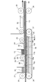
- FIG. 1 is a cross-sectional view of a solar cell manufacturing apparatus according to a first embodiment of the present invention.
- FIG. 4 is a cross-sectional view of a solar cell manufacturing apparatus according to a second embodiment of the present invention.
- P-type silicon powder 11 and N-type silicon powder 12 are prepared.
- the silicon particles of these powders 11 and 12 are substantially spherical, have a particle size of about 0.1-10 ⁇ m, and have a solar cell grade (7 nine level) purity.
- These powders 11 and 12 can be mass-produced by a method for producing high-purity silicon using a rotating crucible of the present inventors (Japanese Patent Application No. 2010-35714).
- the P-type silicon powder 11 is accommodated in the storage unit 21, and the N-type silicon powder 12 is stored in the storage unit 22.
- a transparent insulating foil 13 and a transparent electrode foil 14 bonded thereto are fixed on the plate 35 by rollers 23, 24, 25, 26 and a heat-resistant metal belt 27 at a constant speed below the reservoirs 21 and 22. Sent in the direction. Openings 21 a and 22 a are provided below the storage portions 21 and 22, and the layers are disposed in layers on the transparent electrode foil 14 in which the P-type silicon powder 11 is bonded onto the transparent insulating foil 13 from the opening 21 a.
- the P-type silicon powder layer 11a arranged in layers on the transparent electrode foil 14 is sent in the direction of the arrow in the figure, and heat is applied directly under the heater 28, which is lower than the melting point of silicon (1412 ° C.) 600-1350. Heated to ° C. Then, pressure is applied by the rolling roller 29, and the P-type silicon powder layer 11a in a heated state is fired while being pressed. Thus, by applying heat and pressure, the P-type silicon powder layer 11a is baked while being compressed, and the P-type silicon powder layer 11a becomes a P-type silicon layer 11b which is pressure-sintered.
- silicon particles having a particle size of about 0.1-10 ⁇ m are bonded to each other by diffusion bonding, and a strong bonded state is formed both electrically and mechanically.
- the N-type silicon powder 12 When the P-type silicon layer 11b moves below the reservoir 22, the N-type silicon powder 12 is disposed on the P-type silicon layer 11b, and when the P-type silicon layer 11b passes through the opening 22a, the N-type silicon powder layer 12a becomes the P-type silicon layer 11b. Formed in layers on top. Then, heat is applied directly under the heater 30, heated to 600 to 1350 ° C., and pressure is applied by the rolling roller 31. As a result, the N-type silicon powder layer 12a is baked while being compressed to become a pressure-sintered N-type silicon layer 12b, and the silicon particles are bonded to each other by diffusion bonding. At the same time, the silicon particles of the P-type silicon layer 11b are also bonded by diffusion bonding, and a PN junction is formed at the interface between both layers.
- An electrode foil (aluminum foil or copper foil or the like) 15 is disposed on the upper surface side of the N-type silicon layer 12b, and is joined to the upper surface of the N-type silicon layer 12b by heating with a heater 32. As a result, a PN junction is formed between the P-type silicon layer 11b and the N-type silicon layer 12b, and both the layers 11b and 12b are sandwiched between the two electrode foils 13 and 15, and are formed on the transparent insulating foil 13. Fixed solar cells are continuously formed.
- the manufacturing process of the solar cell is preferably performed in an inert gas atmosphere such as vacuum or Ar.
- the said Example uses the P-type silicon powder 11 and the N-type silicon powder 12 which were doped beforehand as a raw material.
- non-doped silicon powder may be used as a raw material
- a dopant may be added from the dopant inlets 33 and 34
- the P-type or N-type may be doped in the process of pressure firing.
- an I-type silicon layer obtained by pressure-sintering non-doped silicon powder may be provided between the P-type silicon layer 11b and the N-type silicon layer 12b to form a PIN-type junction.
- a P-type silicon powder 11 and an N-type silicon powder 12 are prepared, and a transparent insulating foil 13 and a transparent electrode foil 14 bonded to the rollers 23 and 22 are stored at a constant speed below the storage portions 21 and 22 containing these. It is the same as in the first embodiment that 24, 25, 26 and the belt 27 are sent on the plate 35 in the direction of the arrow in the figure. Accordingly, the P-type silicon powder layer 11a is formed in layers on the transparent electrode foil 14 bonded on the transparent insulating foil 13 from the opening 21a, and the N-type silicon powder layer 12a is formed in layers on the P-type silicon layer 11b from the opening 22a. It is formed.
- the powder layer 11a When the P-type silicon powder layer 11a enters under the heater 41, the powder layer 11a is preheated to 1300 to 1400 ° C., and is heated to 1500 ° C., which is equal to or higher than the melting point (1420 ° C.) of silicon. It is heated above. As a result, the temperature of the powder layer 11a gradually rises due to preheating, bubbles and the like are removed, and the powder layer 11a is melted to exceed the melting point by laser irradiation to be in a liquid state. And it cools with the liquid nitrogen or the water cooling roll 43, and becomes the solid-phase P-type silicon layer 11b. In the P-type silicon layer 11b, silicon is monocrystalline, polycrystalline, or amorphous.
- an N-type silicon powder layer 12a is formed in a layered manner on the P-type silicon layer 11b in the reservoir 22 of the N-type silicon powder 12. Then, in the same manner as described above, preheating is performed by the heater 44, melting is performed by laser irradiation of the laser irradiation device 45, and the liquid phase state is obtained. The cooling roll 46 cools the solid phase N-type silicon layer 12b. At the same time, a PN junction is formed at the interface between the P-type silicon layer 12a and the N-type silicon layer 12b.
- the plate 35 includes a water cooling pipe 35a and a vacuum suction pipe 35b.
- the insulating foil 13 and the electrode foil 14 are cooled by cooling water in the water cooling pipe 35a while adsorbing the insulating foil 13 and the electrode foil 14 by the vacuum suction pipe 35b. Cool down. Therefore, even if the silicon powder layers 11a and 12a are formed on the electrode foil 14 bonded to the insulating foil 13, and the silicon powder layers 11a and 12a are heated at a temperature of 1500 ° C. or more by laser irradiation, the insulating foil 13 and the electrode The temperature of the foil 14 is kept at the temperature of the cooling water and they are not damaged.
- the electrode foil 15 can be tightly fixed to the N-type silicon layer 12b by placing the electrode foil 15 on the upper portion after the formation of the N-type silicon layer 12b and heating it with the heater 32.
- a solar battery cell having P-type and N-type silicon layers 11b and 12b between 15 can be formed by a simple process.
- the present invention enables the production of solar cells from silicon powder. Thereby, a photovoltaic cell can be mass-produced with a simple process and low cost.
Landscapes
- Engineering & Computer Science (AREA)
- Chemical & Material Sciences (AREA)
- Power Engineering (AREA)
- Manufacturing & Machinery (AREA)
- Electromagnetism (AREA)
- General Physics & Mathematics (AREA)
- Computer Hardware Design (AREA)
- Microelectronics & Electronic Packaging (AREA)
- Physics & Mathematics (AREA)
- Condensed Matter Physics & Semiconductors (AREA)
- Chemical Kinetics & Catalysis (AREA)
- Materials Engineering (AREA)
- Mechanical Engineering (AREA)
- Metallurgy (AREA)
- Organic Chemistry (AREA)
- Photovoltaic Devices (AREA)
- Silicon Compounds (AREA)
Abstract
簡素なプロセスで且つ低コストで太陽電池セルを量産可能な、太陽電池セルの製造方法を提供する。第1導電型のシリコン粉末(11)を準備し、前記粉末を層状に配置してシリコン粉末層(11a)を形成し、シリコンの融点以上に加熱することで、前記粉末層を溶融し、冷却することで、第1導電型のシリコン層(11b)を形成し、第2導電型のシリコン粉末(12)を準備し、前記粉末を前記第1導電型のシリコン層(11b)上に層状に配置して第2導電型のシリコン粉末層(12a)を形成し、シリコンの融点以上に加熱することで、前記粉末層を溶融し、冷却することで、第2導電型のシリコン層(12b)を形成する。
Description
本発明は、シリコン粉末を原料とするシリコン太陽電池セルの製造方法に関する。
従来からシリコン太陽電池の形式として、単結晶シリコン型、多結晶シリコン型、微結晶シリコン型、アモルファスシリコン型等が知られている。これらは、高純度シリコンウエハを半導体基板として利用し、或いは絶縁性または導電性基板上にCVD法或いは蒸着法等を用いてシリコン膜を形成し、PN接合或いはPIN接合を形成するものである。
現在、地球温暖化防止の観点等から、太陽電池の普及が要請されているが、そのコスト低減が課題であることは周知のとおりである。
本発明は、簡素なプロセスで且つ低コストで太陽電池セルを量産可能な、太陽電池セルの製造方法を提供することを目的とする。
本発明の太陽電池セルの製造方法は、第1導電型のシリコン粉末を準備し、前記粉末を層状に配置してシリコン粉末層を形成し、シリコンの融点以上に加熱することで、前記粉末層を溶融し、冷却することで、第1導電型のシリコン層を形成し、第2導電型のシリコン粉末を準備し、前記粉末を前記第1導電型のシリコン層上に層状に配置して第2導電型のシリコン粉末層を形成し、シリコンの融点以上に加熱することで、前記粉末層を溶融し、冷却することで、第2導電型のシリコン層を形成する、ことを特徴とする。
また、本発明の太陽電池セルの製造方法は、第1のシリコン粉末を準備し、前記粉末を層状に配置してシリコン粉末層を形成し、熱と圧力を加えることで、前記粉末層を圧縮しつつ焼成し、第1導電型のシリコン層となし、第2のシリコン粉末を準備し、前記粉末を前記第1導電型のシリコン層上に層状に配置して第2のシリコン粉末層を形成し、熱と圧力を加えることで、前記粉末層を圧縮しつつ焼成し、第2導電型のシリコン層となす、ことを特徴とする。
本発明によれば、シリコン粉末から太陽電池セルを製造可能である。第1導電型のシリコン粉末層を形成し、熱を加えることで、粉末層を溶融し、冷却することで、第1導電型のシリコン層を形成し、該シリコン層上に第2導電型のシリコン粉末層を形成し、熱を加えることで、該粉末層を溶融し、冷却することで、第2導電型のシリコン層を形成するので、PN接合を備えた太陽電池セルを連続的に簡易なプロセスで製造できる。また、熱と圧力を加えることで、前記粉末層を圧縮しつつ焼成するようにしてもよい。
以下、本発明の第1実施例について、図1を参照して説明する。まず、P型シリコン粉末11およびN型シリコン粉末12を準備する。これら粉末11,12のシリコン粒子は略球形であり、0.1-10μm程度の粒径を有し、太陽電池級(7ナインレベル)の純度を有する。これら粉末11,12は、本発明者等の回転ルツボを用いた高純度シリコンの製造方法(特願2010-35714)等により量産が可能である。
P型シリコン粉末11は貯留部21に収容され、N型シリコン粉末12は貯留部22に収容される。貯留部21,22の下側には透明絶縁箔13とこれに接合した透明電極箔14とが一定速度でローラ23,24,25,26および耐熱金属ベルト27によりプレート35上を図中の矢印方向に送られる。貯留部21,22の下側には開口21a,22aを備え、開口21aからP型シリコン粉末11を透明絶縁箔13上に接合した透明電極箔14上に層状に配置する。
透明電極箔14上に層状に配置したP型シリコン粉末層11aは、図中の矢印方向に送られ、ヒータ28の直下で熱が加えられ、シリコンの融点(1412℃)よりも低い600-1350℃に加熱される。そして、圧延ローラ29により圧力が加えられ、熱を加えた状態のP型シリコン粉末層11aを加圧しつつ焼成する。このように、熱と圧力を加えることで、P型シリコン粉末層11aを圧縮しつつ焼成し、P型シリコン粉末層11aは加圧燒結したP型シリコン層11bとなる。P型シリコン層11bでは、0.1-10μm程度の粒径を有するシリコン粒子が相互に拡散接合で接合され、電気的にも機械的にも強固な接合状態が形成される。
P型シリコン層11bが貯留部22の下に移動すると、N型シリコン粉末12がP型シリコン層11bの上に配置され、開口22aを通過すると、N型シリコン粉末層12aがP型シリコン層11b上に層状に形成される。そして、ヒータ30の直下で熱が加えられ、600-1350℃に加熱され、圧延ローラ31により圧力が加えられる。これにより、N型シリコン粉末層12aは圧縮しつつ焼成され、加圧燒結したN型シリコン層12bになり、シリコン粒子が相互に拡散接合で接合される。同時に、P型シリコン層11bのシリコン粒子とも拡散接合で接合し、両層の界面にPN接合が形成される。
N型シリコン層12bの上面側には電極箔(アルミ箔または銅箔等)15が配置され、ヒータ32で加熱することで、N型シリコン層12bの上面と接合する。これにより、P型シリコン層11bとN型シリコン層12bとの間にPN接合が形成され、両層11b,12bが2層の電極箔13,15の間に挟まれ、透明絶縁箔13上に固定した太陽電池セルが連続的に形成される。
従って、これを適当な寸法で切り出すことで、太陽電池パネルを量産することができる。この太陽電池パネルの厚みを全体で40μm以下程度とすることで、軽量で且つフレキシブルな太陽電池パネルとすることができる。上記太陽電池の製造工程は真空またはAr等の不活性ガス雰囲気下で行うことが好ましい。
なお、上記実施例は、原料として予めドーピングしたP型シリコン粉末11およびN型シリコン粉末12を用いている。しかしながら、原料としてノンドープのシリコン粉末を用い、ドーパント注入口33,34からドーパントを加え、加圧焼成の過程でP型またはN型にドープするようにしてもよい。
また、P型シリコン層11bとN型シリコン層12bとの間にノンドープのシリコン粉末を加圧焼結したI型シリコン層を設け、PIN型の接合としてもよい。
次に、本発明の第2実施例について、図2を参照して説明する。P型シリコン粉末11およびN型シリコン粉末12を準備し、これらを収容した貯留部21,22の下側には透明絶縁箔13とこれに接合した透明電極箔14とが一定速度でローラ23,24,25,26およびベルト27によりプレート35上を図中の矢印方向に送られることは第1実施例と同様である。従って、開口21aからP型シリコン粉末層11aが透明絶縁箔13上に接合した透明電極箔14上に層状に形成され、開口22aからN型シリコン粉末層12aがP型シリコン層11b上に層状に形成される。
P型シリコン粉末層11aがヒータ41の下に入ると、粉末層11aは1300-1400℃に予備加熱され、レーザ照射装置42によるレーザ加熱によりシリコンの融点(1420℃)以上の温度である1500℃以上に加熱される。これにより、粉末層11aは予備加熱により緩やかに温度上昇し、気泡等が取り除かれ、レーザ照射により融点を超え溶融し液相状態となる。そして、液体窒素または水冷却ロール43により冷却され、固相のP型シリコン層11bとなる。P型シリコン層11bではシリコンは単結晶または多結晶或いは非晶質をなしている。
次に、N型シリコン粉末12の貯留部22にてN型シリコン粉末層12aがP型シリコン層11b上に層状に形成される。そして、上述と同様に、ヒータ44により予備加熱し、レーザ照射装置45のレーザ照射により溶融し液相状態となり、冷却ロール46により冷却され、固相のN型シリコン層12bとなる。同時に、P型シリコン層12aとN型シリコン層12bとの界面にはPN接合が形成される。
プレート35は内部に水冷配管35aと真空吸着配管35bとを備え、該真空吸着配管35bにより絶縁箔13と電極箔14を吸着しつつ、水冷配管35a中の冷却水により絶縁箔13と電極箔14を冷却する。従って、絶縁箔13に接合した電極箔14上にシリコン粉末層11a,12aを形成し、シリコン粉末層11a,12aの加熱をレーザ照射で1500℃以上の温度で行っても、絶縁箔13と電極箔14の温度は冷却水の温度に保たれ、これらは損傷することがない。
このため、N型シリコン層12bの形成後電極箔15をその上部に配置し、ヒータ32で加熱することで、電極箔15をN型シリコン層12bに密着固定することができ、電極箔14,15間にP型とN型のシリコン層11b,12bを備えた太陽電池セルを簡素なプロセスで形成できる。
これまで本発明の一実施例について説明したが、本発明は上述の実施形態に限定されず、その技術的思想の範囲内において種々異なる形態にて実施されてよいことは言うまでもない。
本発明は、シリコン粉末から太陽電池セルの製造を可能とするものである。これにより、簡素なプロセスで且つ低コストで、太陽電池セルを量産することができる。
Claims (9)
- 第1導電型のシリコン粉末を準備し、
前記粉末を層状に配置してシリコン粉末層を形成し、
シリコンの融点以上に加熱することで、前記粉末層を溶融し、冷却することで、第1導電型のシリコン層を形成し、
第2導電型のシリコン粉末を準備し、
前記粉末を前記第1導電型のシリコン層上に層状に配置して第2導電型のシリコン粉末層を形成し、
シリコンの融点以上に加熱することで、前記粉末層を溶融し、冷却することで、第2導電型のシリコン層を形成する、太陽電池セルの製造方法。 - 絶縁箔に接合した電極箔上に前記シリコン粉末層を形成し、
プレート内部に水冷配管と真空吸着配管とを備え、該真空吸着配管により前記絶縁箔と前記電極箔を吸着しつつ、前記水冷配管中の冷却水により前記絶縁箔と前記電極箔を冷却しつつ、前記シリコン粉末層の加熱を前記プレート上で行う、請求項1に記載の太陽電池セルの製造方法。 - 前記加熱はヒータを用いて前記粉末層を予備加熱し、さらにレーザ照射により溶融する、請求項1に記載の太陽電池セルの製造方法。
- 第1のシリコン粉末を準備し、
前記粉末を層状に配置してシリコン粉末層を形成し、
熱と圧力を加えることで、前記粉末層を圧縮しつつ焼成し、第1導電型のシリコン層となし、
第2のシリコン粉末を準備し、
前記粉末を前記第1導電型のシリコン層上に層状に配置して第2のシリコン粉末層を形成し、
熱と圧力を加えることで、前記粉末層を圧縮しつつ焼成し、第2導電型のシリコン層となす、太陽電池セルの製造方法。 - 前記シリコン粉末の粒子は0.1-10μmの粒径を有する、請求項4に記載の太陽電池セルの製造方法。
- 前記熱はヒータを用いて発生し、前記粉末層を600-1200℃に加熱する、請求項4に記載の太陽電池セルの製造方法。
- 前記圧力は圧延ローラを用いて発生し、熱を加えた状態の前記粉末層を加圧しつつ焼成する、請求項4に記載の太陽電池セルの製造方法。
- 前記粉末のシリコン粒子は予めP型またはN型にドープしたものである、請求項4に記載の太陽電池セルの製造方法。
- 前記粉末のシリコン粒子はノンドープであり、ドーパントを加えて加圧焼成の過程で、P型またはN型にドープする、請求項4に記載の太陽電池セルの製造方法。
Priority Applications (4)
| Application Number | Priority Date | Filing Date | Title |
|---|---|---|---|
| CN201180010870.1A CN102834926B (zh) | 2010-02-25 | 2011-02-25 | 使用了硅粉末的太阳能电池单体的制造方法 |
| EP11747494.0A EP2541616B1 (en) | 2010-02-25 | 2011-02-25 | Method for manufacturing solar cell using silicon powder |
| JP2012501876A JP5761172B2 (ja) | 2010-02-25 | 2011-02-25 | シリコン粉末を用いた太陽電池セルの製造方法 |
| US13/591,628 US8603850B2 (en) | 2010-02-25 | 2012-08-22 | Method for manufacturing solar cell using silicon powder |
Applications Claiming Priority (2)
| Application Number | Priority Date | Filing Date | Title |
|---|---|---|---|
| JP2010039497 | 2010-02-25 | ||
| JP2010-039497 | 2010-02-25 |
Related Child Applications (1)
| Application Number | Title | Priority Date | Filing Date |
|---|---|---|---|
| US13/591,628 Continuation US8603850B2 (en) | 2010-02-25 | 2012-08-22 | Method for manufacturing solar cell using silicon powder |
Publications (1)
| Publication Number | Publication Date |
|---|---|
| WO2011105538A1 true WO2011105538A1 (ja) | 2011-09-01 |
Family
ID=44506935
Family Applications (1)
| Application Number | Title | Priority Date | Filing Date |
|---|---|---|---|
| PCT/JP2011/054255 WO2011105538A1 (ja) | 2010-02-25 | 2011-02-25 | シリコン粉末を用いた太陽電池セルの製造方法 |
Country Status (5)
| Country | Link |
|---|---|
| US (1) | US8603850B2 (ja) |
| EP (1) | EP2541616B1 (ja) |
| JP (1) | JP5761172B2 (ja) |
| CN (1) | CN102834926B (ja) |
| WO (1) | WO2011105538A1 (ja) |
Families Citing this family (2)
| Publication number | Priority date | Publication date | Assignee | Title |
|---|---|---|---|---|
| US11764315B2 (en) * | 2020-09-16 | 2023-09-19 | Maxeon Solar Pte. Ltd. | Solar cell separation with edge coating |
| CN115224238B (zh) * | 2022-09-20 | 2022-11-29 | 河南锂动电源有限公司 | 一种锂离子电池负极极片及其制作方法和激光碳化装置 |
Citations (3)
| Publication number | Priority date | Publication date | Assignee | Title |
|---|---|---|---|---|
| JP2002151713A (ja) * | 2000-08-29 | 2002-05-24 | Kyocera Corp | 太陽電池素子基板及びその製造方法 |
| JP2009246041A (ja) * | 2008-03-28 | 2009-10-22 | Mitsubishi Electric Corp | 太陽電池およびその製造方法 |
| JP2010035714A (ja) | 2008-08-01 | 2010-02-18 | Canon Inc | X線画像診断装置および制御方法 |
Family Cites Families (17)
| Publication number | Priority date | Publication date | Assignee | Title |
|---|---|---|---|---|
| DE3035563C2 (de) * | 1980-09-20 | 1984-10-11 | Licentia Patent-Verwaltungs-Gmbh, 6000 Frankfurt | Verfahren zum Herstellen einer polykristallinen Silizium-Solarzelle |
| DE3536743C2 (de) * | 1985-10-15 | 1994-11-10 | Siemens Ag | Verfahren zum Herstellung von großflächigen Siliziumkristallkörpern für Solarzellen |
| JPH06268242A (ja) * | 1993-03-17 | 1994-09-22 | Matsushita Electric Ind Co Ltd | シリコン基板の製造方法および結晶質シリコン太陽電池 |
| ATE175625T1 (de) * | 1993-06-11 | 1999-01-15 | Isovolta | Verfahren zur herstellung fotovoltaischer module sowie eine vorrichtung zur durchführung dieses verfahrens |
| DE19652818A1 (de) * | 1996-12-18 | 1998-07-02 | Priesemuth W | Verfahren zum Herstellen einer Solarzelle sowie Solarzelle |
| JP2001516324A (ja) * | 1997-03-04 | 2001-09-25 | アストロパワー,インコーポレイテッド | 柱状結晶粒状多結晶太陽電池基材及び改良された製造方法 |
| JP2001250967A (ja) * | 2000-03-03 | 2001-09-14 | Canon Inc | 光起電力素子及び光起電力素子の製造方法 |
| JP4140247B2 (ja) * | 2002-03-04 | 2008-08-27 | 独立行政法人産業技術総合研究所 | シート型β−FeSi2素子 |
| DE10239845C1 (de) * | 2002-08-29 | 2003-12-24 | Day4 Energy Inc | Elektrode für fotovoltaische Zellen, fotovoltaische Zelle und fotovoltaischer Modul |
| US8192648B2 (en) * | 2003-04-14 | 2012-06-05 | S'tile | Method for forming a sintered semiconductor material |
| US8405183B2 (en) * | 2003-04-14 | 2013-03-26 | S'Tile Pole des Eco-Industries | Semiconductor structure |
| US20080305619A1 (en) * | 2007-05-03 | 2008-12-11 | Francesco Lemmi | Method of forming group iv semiconductor junctions using laser processing |
| JP4990738B2 (ja) * | 2007-11-09 | 2012-08-01 | 株式会社ブリヂストン | 太陽電池の製造方法 |
| US20090208770A1 (en) * | 2008-02-14 | 2009-08-20 | Ralf Jonczyk | Semiconductor sheets and methods for fabricating the same |
| US20090280336A1 (en) * | 2008-05-08 | 2009-11-12 | Ralf Jonczyk | Semiconductor sheets and methods of fabricating the same |
| JP2010206161A (ja) * | 2009-02-04 | 2010-09-16 | Sony Corp | 成膜方法および半導体装置の製造方法 |
| JP2011116616A (ja) | 2009-10-29 | 2011-06-16 | Sanki Dengyo Kk | 回転ルツボ装置を用いた高純度シリコンの製造方法 |
-
2011
- 2011-02-25 WO PCT/JP2011/054255 patent/WO2011105538A1/ja active Application Filing
- 2011-02-25 EP EP11747494.0A patent/EP2541616B1/en not_active Not-in-force
- 2011-02-25 JP JP2012501876A patent/JP5761172B2/ja not_active Expired - Fee Related
- 2011-02-25 CN CN201180010870.1A patent/CN102834926B/zh not_active Expired - Fee Related
-
2012
- 2012-08-22 US US13/591,628 patent/US8603850B2/en not_active Expired - Fee Related
Patent Citations (3)
| Publication number | Priority date | Publication date | Assignee | Title |
|---|---|---|---|---|
| JP2002151713A (ja) * | 2000-08-29 | 2002-05-24 | Kyocera Corp | 太陽電池素子基板及びその製造方法 |
| JP2009246041A (ja) * | 2008-03-28 | 2009-10-22 | Mitsubishi Electric Corp | 太陽電池およびその製造方法 |
| JP2010035714A (ja) | 2008-08-01 | 2010-02-18 | Canon Inc | X線画像診断装置および制御方法 |
Non-Patent Citations (1)
| Title |
|---|
| See also references of EP2541616A4 * |
Also Published As
| Publication number | Publication date |
|---|---|
| JPWO2011105538A1 (ja) | 2013-06-20 |
| EP2541616A4 (en) | 2014-01-29 |
| JP5761172B2 (ja) | 2015-08-12 |
| CN102834926A (zh) | 2012-12-19 |
| EP2541616A1 (en) | 2013-01-02 |
| CN102834926B (zh) | 2015-07-22 |
| EP2541616B1 (en) | 2016-05-04 |
| US8603850B2 (en) | 2013-12-10 |
| US20130045559A1 (en) | 2013-02-21 |
Similar Documents
| Publication | Publication Date | Title |
|---|---|---|
| US8105923B2 (en) | Sintered semiconductor material | |
| US8110285B2 (en) | Self-supported film and silicon wafer obtained by sintering | |
| US9493358B2 (en) | Photovoltaic module including integrated photovoltaic cells | |
| US20150236173A1 (en) | Photovaltaic device conducting layer | |
| JPWO2011048797A1 (ja) | 結晶型太陽電池パネルの製造方法 | |
| US8420515B2 (en) | Method of producing a solar cell | |
| US11152556B2 (en) | Flexible and conformable thermoelectric compositions | |
| JP5761172B2 (ja) | シリコン粉末を用いた太陽電池セルの製造方法 | |
| CN101570321A (zh) | 一种高性能纳米结构BixSbyTe3-z热电材料的制备方法 | |
| TWI506807B (zh) | 太陽能電池製造方法 | |
| US4602422A (en) | Flash compression process for making photovoltaic cells | |
| TW202143514A (zh) | 熱電變換體、熱電變換模組、及熱電變換體之製造方法 | |
| JP4869196B2 (ja) | 回転式拡散装置および光電変換装置の製造方法 | |
| JP2013177264A (ja) | Si微細粒子による薄膜層の形成方法、半導体装置および半導体装置の製造方法、並びに太陽電池および太陽電池の製造方法。 | |
| JP2006156584A (ja) | 結晶シリコン粒子への不純物の拡散方法および光電変換装置ならびに光発電装置 | |
| US9741881B2 (en) | Photovoltaic module including integrated photovoltaic cells | |
| US9620664B2 (en) | Coating of graphite tooling for manufacture of semiconductors | |
| JP4869195B2 (ja) | 光電変換装置の製造方法 | |
| RU2520480C1 (ru) | Способ получения слоев карбида кремния | |
| KR20200017848A (ko) | 웨이퍼 없는 수직 적층형 태양전지와 그 제조방법 | |
| JP2009194011A (ja) | 半導体ウエハの不純物拡散方法及び半導体基体の製造方法 | |
| CN117702268A (zh) | 一种单晶硅棒及其制得的硅片、电池和电池组件 | |
| JP5532240B2 (ja) | 半導体粒子の製造方法 | |
| JP2007173425A (ja) | 光電変換装置の製造方法および光発電装置 | |
| CN102082197A (zh) | 局限液相磊晶层形成方法 |
Legal Events
| Date | Code | Title | Description |
|---|---|---|---|
| WWE | Wipo information: entry into national phase |
Ref document number: 201180010870.1 Country of ref document: CN |
|
| 121 | Ep: the epo has been informed by wipo that ep was designated in this application |
Ref document number: 11747494 Country of ref document: EP Kind code of ref document: A1 |
|
| WWE | Wipo information: entry into national phase |
Ref document number: 2012501876 Country of ref document: JP |
|
| NENP | Non-entry into the national phase |
Ref country code: DE |
|
| WWE | Wipo information: entry into national phase |
Ref document number: 2011747494 Country of ref document: EP |