WO2011105315A1 - フィルタ、デュープレクサ、通信モジュール、通信装置 - Google Patents
フィルタ、デュープレクサ、通信モジュール、通信装置 Download PDFInfo
- Publication number
- WO2011105315A1 WO2011105315A1 PCT/JP2011/053629 JP2011053629W WO2011105315A1 WO 2011105315 A1 WO2011105315 A1 WO 2011105315A1 JP 2011053629 W JP2011053629 W JP 2011053629W WO 2011105315 A1 WO2011105315 A1 WO 2011105315A1
- Authority
- WO
- WIPO (PCT)
- Prior art keywords
- filter
- inductor
- parallel
- resonator
- ladder
- Prior art date
- Legal status (The legal status is an assumption and is not a legal conclusion. Google has not performed a legal analysis and makes no representation as to the accuracy of the status listed.)
- Ceased
Links
Images




Classifications
-
- H—ELECTRICITY
- H03—ELECTRONIC CIRCUITRY
- H03H—IMPEDANCE NETWORKS, e.g. RESONANT CIRCUITS; RESONATORS
- H03H9/00—Networks comprising electromechanical or electro-acoustic elements; Electromechanical resonators
- H03H9/46—Filters
- H03H9/54—Filters comprising resonators of piezoelectric or electrostrictive material
- H03H9/58—Multiple crystal filters
- H03H9/60—Electric coupling means therefor
- H03H9/605—Electric coupling means therefor consisting of a ladder configuration
-
- H—ELECTRICITY
- H03—ELECTRONIC CIRCUITRY
- H03H—IMPEDANCE NETWORKS, e.g. RESONANT CIRCUITS; RESONATORS
- H03H9/00—Networks comprising electromechanical or electro-acoustic elements; Electromechanical resonators
- H03H9/46—Filters
- H03H9/54—Filters comprising resonators of piezoelectric or electrostrictive material
- H03H9/542—Filters comprising resonators of piezoelectric or electrostrictive material including passive elements
-
- H—ELECTRICITY
- H03—ELECTRONIC CIRCUITRY
- H03H—IMPEDANCE NETWORKS, e.g. RESONANT CIRCUITS; RESONATORS
- H03H9/00—Networks comprising electromechanical or electro-acoustic elements; Electromechanical resonators
- H03H9/46—Filters
- H03H9/54—Filters comprising resonators of piezoelectric or electrostrictive material
- H03H9/56—Monolithic crystal filters
- H03H9/566—Electric coupling means therefor
- H03H9/568—Electric coupling means therefor consisting of a ladder configuration
-
- H—ELECTRICITY
- H03—ELECTRONIC CIRCUITRY
- H03H—IMPEDANCE NETWORKS, e.g. RESONANT CIRCUITS; RESONATORS
- H03H9/00—Networks comprising electromechanical or electro-acoustic elements; Electromechanical resonators
- H03H9/46—Filters
- H03H9/64—Filters using surface acoustic waves
- H03H9/6423—Means for obtaining a particular transfer characteristic
- H03H9/6433—Coupled resonator filters
- H03H9/6483—Ladder SAW filters
-
- H—ELECTRICITY
- H03—ELECTRONIC CIRCUITRY
- H03H—IMPEDANCE NETWORKS, e.g. RESONANT CIRCUITS; RESONATORS
- H03H9/00—Networks comprising electromechanical or electro-acoustic elements; Electromechanical resonators
- H03H9/70—Multiple-port networks for connecting several sources or loads, working on different frequencies or frequency bands, to a common load or source
- H03H9/703—Networks using bulk acoustic wave devices
- H03H9/706—Duplexers
-
- H—ELECTRICITY
- H03—ELECTRONIC CIRCUITRY
- H03H—IMPEDANCE NETWORKS, e.g. RESONANT CIRCUITS; RESONATORS
- H03H9/00—Networks comprising electromechanical or electro-acoustic elements; Electromechanical resonators
- H03H9/70—Multiple-port networks for connecting several sources or loads, working on different frequencies or frequency bands, to a common load or source
- H03H9/72—Networks using surface acoustic waves
- H03H9/725—Duplexers
-
- H—ELECTRICITY
- H03—ELECTRONIC CIRCUITRY
- H03H—IMPEDANCE NETWORKS, e.g. RESONANT CIRCUITS; RESONATORS
- H03H7/00—Multiple-port networks comprising only passive electrical elements as network components
- H03H7/01—Frequency selective two-port networks
- H03H7/0123—Frequency selective two-port networks comprising distributed impedance elements together with lumped impedance elements
-
- H—ELECTRICITY
- H03—ELECTRONIC CIRCUITRY
- H03H—IMPEDANCE NETWORKS, e.g. RESONANT CIRCUITS; RESONATORS
- H03H7/00—Multiple-port networks comprising only passive electrical elements as network components
- H03H7/01—Frequency selective two-port networks
- H03H7/0138—Electrical filters or coupling circuits
-
- H—ELECTRICITY
- H03—ELECTRONIC CIRCUITRY
- H03H—IMPEDANCE NETWORKS, e.g. RESONANT CIRCUITS; RESONATORS
- H03H7/00—Multiple-port networks comprising only passive electrical elements as network components
- H03H7/01—Frequency selective two-port networks
- H03H7/075—Ladder networks, e.g. electric wave filters
-
- H—ELECTRICITY
- H03—ELECTRONIC CIRCUITRY
- H03H—IMPEDANCE NETWORKS, e.g. RESONANT CIRCUITS; RESONATORS
- H03H7/00—Multiple-port networks comprising only passive electrical elements as network components
- H03H7/46—Networks for connecting several sources or loads, working on different frequencies or frequency bands, to a common load or source
- H03H7/463—Duplexers
Definitions
- the present disclosure relates to a filter, a duplexer, a communication module, and a communication device.
- Patent Documents 1 and 2 disclose a configuration in which an inductor is added to a ladder type filter to improve filter characteristics.
- the filter disclosed in the present application includes a plurality of main resonators connected to a series arm, a plurality of sub-resonators connected to a parallel arm, and at least one main resonator among the plurality of main resonators.
- a sub-resonator comprising: a connected main inductor; and a sub-inductor connected to at least one sub-resonator among the plurality of sub-resonators, wherein the main resonator and the sub-inductor are connected in parallel.
- the main inductor is arranged so that the main inductor is not connected to the path between the two.
- the duplexer disclosed in the present application includes the above-described filter.
- the communication module disclosed in the present application includes the above-described filter.
- the communication device disclosed in the present application includes the above-described filter.
- FIG. 4 is a characteristic diagram showing the pass characteristic of the filter shown in FIG. Circuit diagram of ladder filter on input side and output side
- FIG. 6 is a characteristic diagram showing the pass characteristics of the filter shown in FIG. Duplexer block diagram Communication module block diagram Block diagram of communication device
- FIG. 1 is a circuit diagram of a ladder filter as a comparative example.
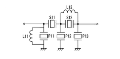
- FIG. 2 is a circuit diagram of a ladder type filter as an embodiment.
- FIG. 3 shows the pass characteristics of the ladder filters shown in FIGS. 1 and 2. Characteristics (a) to (d) in FIG. 3 are characteristics of the ladder type filter shown in FIGS. 1 (a) to (d), respectively.
- series resonators S1 and S2 are connected to a series arm, and parallel resonators P1 to P3 are connected to a parallel arm.
- the series resonators S1 and S2 and the parallel resonators P1 to P3 can be realized by FBARs, for example.
- the resonance frequency of the series resonators S1 and S2 is, for example, 3.7 GHz.
- the resonant frequency of the parallel resonators P1 to P3 is, for example, 3.5 GHz.
- an inductor L1 is connected in parallel to the parallel resonator P1.
- an inductor L1 is connected in parallel to the parallel resonator P1, and an inductor L2 is connected in parallel to the parallel resonator P3.
- the values of the inductors L1 and L2 are, for example, 4.6 nH.
- series resonators S3 and S4 are connected to the series arm, and parallel resonators P1 to P3 are connected to the parallel arm.
- an inductor L3 is connected in parallel to the series resonator S4.
- the resonance frequency of the series resonator S3 is, for example, 3.75 GHz.
- the resonance frequency of the series resonator S4 is, for example, 3.6 GHz.
- the resonant frequency of the parallel resonators P1 to P3 is, for example, 3.5 GHz.
- the value of the inductor L3 is 2 nH, for example.
- the signal in the frequency band near the center of the pass band is greatly attenuated and the loss becomes large.
- FIGS. 1B to 1D by connecting an inductor to the resonator included in the ladder type filter, as shown in characteristics (b) to (D) in FIG.
- the attenuation amount in the frequency band near the center of the band can be reduced as compared with the attenuation amount in the characteristic (a).
- the characteristics (b) to (d) in FIG. 3 are low-loss passing characteristics.
- an inductor L11 is connected in parallel to the parallel resonator P11, and an inductor L12 is connected in parallel to the series resonator S12.
- the inductor L11 is connected on the path between the series resonator S11 and the parallel resonator P11.
- the inductor L12 is connected to a path between the series resonator S12 and the parallel resonator P12 and a path between the series resonator S12 and the parallel resonator P13. That is, the path between the inductors L11 and the path between the inductors L12 are at different positions.
- the resonance frequency of the series resonator S11 is, for example, 3.75 GHz.
- the resonance frequency of the series resonator S12 is, for example, 3.6 GHz.
- the resonant frequency of the parallel resonators P11 to P13 is, for example, 3.5 GHz.
- the value of the inductor L11 is, for example, 4.6 nH.
- the value of the inductor L12 is 2 nH, for example.
- the difference between the ladder type filter as the comparative example shown in FIG. 1 and the ladder type filter as the embodiment shown in FIG. 2 is that one of the inductors is connected to the series arm and the other inductor is the parallel arm. It is a point connected to.
- the attenuation in the frequency band near the center of the pass band can be suppressed as compared with the characteristics (a) to (d) as shown by the characteristic A in FIG. be able to.
- the bandwidth of the pass band can be expanded as compared with the bandwidths shown in the characteristics (a) to (c).
- the pass characteristics of the filter not only connect the inductor to the series arm and the parallel arm in the ladder type filter, but also change depending on the location where the inductor is connected.
- the relationship between the connection location of the inductor and the pass characteristic of the ladder filter will be described.
- FIG. 4A a ladder filter in which an inductor L11 is connected in parallel to the parallel resonator P11 and an inductor L12 is connected in parallel to the series resonator S12.
- FIG. 4B shows a ladder filter in which an inductor L21 is connected in parallel to the parallel resonator P21, and an inductor L22 is connected in parallel to the series resonator S21.
- the inductors L21 and L22 are connected on a path between the series resonator S21 and the parallel resonator P21.
- an inductor L31 is connected in parallel to the parallel resonator P31
- an inductor L32 is connected in parallel to the series resonator S31
- an inductor L33 is connected in parallel to the parallel resonator P33.
- It is a ladder type filter.
- the inductors L31 and L32 are connected on the path between the series resonator S31 and the parallel resonator P31.
- the constants of the resonators and the inductors are the same as those of the resonator and the inductor shown in FIG.
- FIG. 5 shows the pass characteristics of the ladder type filter shown in FIGS. 4 (a) to 4 (c).
- the characteristics (a) in FIG. When the inductor L11 and the inductor L12 are connected on different paths (on the path between the series arm and the parallel arm), the characteristics (a) in FIG. Thus, the attenuation is not increased near the center of the passband, and a low-loss pass characteristic is obtained.
- the attenuation near the center of the passband can be made smaller than the characteristic (b) as shown in the characteristic (c) in FIG.
- the attenuation near the center of the passband is larger than the attenuation shown in the characteristic (a), and it is difficult to say that the characteristic (c) has a low loss.
- FIG. 6A shows a two-stage ladder filter on the input side in the ladder filter shown in FIG.
- FIG. 6B shows a two-stage ladder filter on the output side in the ladder filter shown in FIG.
- FIG. 6C shows a ladder filter for two stages on the input side in the ladder filter shown in FIG.
- FIG. 6D shows a two-stage ladder filter on the output side in the ladder filter shown in FIG. Note that the number of stages of the ladder filter is counted as one stage with one series resonator and one parallel resonator.
- the ladder type filter constituted by the series resonator S11 and the parallel resonator P11 is the first-stage ladder type filter, and is constituted by the series resonator S11 and the parallel resonator P12.
- the ladder type filter is a second stage ladder type filter.
- FIG. 7 shows the pass characteristics of the ladder filter shown in FIGS. 6 (a) to 6 (d). Characteristics (a) to (d) in FIG. 7 correspond to the pass characteristics of the ladder type filters shown in FIGS. 6 (a) to (d), respectively.
- the pass characteristic combining the characteristic (a) and the characteristic (b) shown in FIG. Become.
- the ladder type filter including the ladder type filter shown in FIG. 6C and the ladder type filter shown in FIG. 6D the combination of the characteristics (c) and the characteristics (d) shown in FIG. It becomes a characteristic. That is, according to the ladder type filter including the ladder type filter shown in FIG.
- the ladder type filter shown in FIG. 6A and the ladder type filter shown in FIG. 6B that is, the ladder type filter shown in FIG. Since the impedance can be matched, a low loss and a wide band can be achieved.
- the ladder type filter including the ladder type filter shown in FIG. 6C and the ladder type filter shown in FIG. 6D that is, the ladder type filter shown in FIG. It is difficult to match the impedance, and it is difficult to reduce the loss and increase the bandwidth.
- each resonator is realized by FBAR, but even if it is realized by a SAW device, the same effect as this embodiment can be obtained.
- a duplexer is mounted in mobile communication (high-frequency wireless communication) such as a mobile phone terminal, a PHS (Personal Handy-phone System) terminal, and a wireless LAN system.
- the duplexer has a transmission function and a reception function for communication radio waves and the like, and is used in a wireless device in which frequencies of a transmission signal and a reception signal are different.
- FIG. 8 shows a configuration of a duplexer including the filter according to the present embodiment.
- the duplexer 52 includes a phase matching circuit 53, a reception filter 54, and a transmission filter 55.
- the phase matching circuit 53 is an element for adjusting the phase of the impedance of the reception filter 54 in order to prevent the transmission signal output from the transmission filter 55 from flowing into the reception filter 54 side.
- An antenna 51 is connected to the phase matching circuit 53.
- the reception filter 54 is configured by a band-pass filter that allows only a predetermined frequency band of the reception signal input via the antenna 51 to pass.
- An output terminal 56 is connected to the reception filter 54.
- the transmission filter 55 is configured by a band pass filter that allows only a predetermined frequency band among the transmission signals input via the input terminal 57 to pass.
- An input terminal 57 is connected to the transmission filter 55.
- the reception filter 54 includes the filter in the present embodiment.
- the reception filter 54 shown in FIG. 8 is balanced on the output side, but may be single-ended.
- FIG. 9 shows an example of a communication module including a duplexer according to the present embodiment.
- the duplexer 52 includes a reception filter 54 and a transmission filter 55.
- the reception filter 54 is connected to a reception terminal 56 corresponding to, for example, a balance output.
- the transmission filter 55 is connected to the transmission terminal 57 via the power amplifier 74.
- the reception filter 54 includes the filter according to the present embodiment.
- the reception filter 54 When performing the reception operation, the reception filter 54 passes only a signal in a predetermined frequency band among reception signals input via the antenna terminal 61 and outputs the signal from the reception terminal 56 to the outside. Further, when performing a transmission operation, the transmission filter 55 passes only a signal in a predetermined frequency band among transmission signals input from the transmission terminal 57 and amplified by the power amplifier 74, and outputs the signal from the antenna terminal 61 to the outside. To do.
- the configuration of the communication module shown in FIG. 9 is an example, and the same effect can be obtained even if the duplexer according to the present embodiment is mounted on a communication module of another form.
- FIG. 10 shows an RF block of a mobile phone terminal as an example of a duplexer according to the present embodiment or a communication device including the above-described communication module.
- the communication apparatus shown in FIG. 10 shows a configuration of a mobile phone terminal that supports a GSM (Global System for Mobile Communications) communication system and a W-CDMA (Wideband Code Division Multiple Access) communication system.
- the GSM communication system in the present embodiment corresponds to the 850 MHz band, 950 MHz band, 1.8 GHz band, and 1.9 GHz band.
- the mobile phone terminal includes a microphone, a speaker, a liquid crystal display, and the like. However, illustration is omitted because it is not necessary in the description of the present embodiment.
- the reception filter 54 in the duplexer 52 includes the filter according to the present embodiment.
- the received signal input through the antenna 71 selects an LSI to be operated by the antenna switch circuit 72 depending on whether the communication method is W-CDMA or GSM.
- the input received signal is compatible with the W-CDMA communication system, switching is performed so that the received signal is output to the duplexer 52.
- the reception signal input to the duplexer 52 is limited to a predetermined frequency band by the reception filter 54, and a balanced reception signal is output to the LNA 73.
- the LNA 73 amplifies the input received signal and outputs it to the LSI 75.
- the LSI 75 performs a demodulation process on the audio signal based on the input received signal, and controls the operation of each unit in the mobile phone terminal.
- the LSI 75 when transmitting a signal, the LSI 75 generates a transmission signal.
- the generated transmission signal is amplified by the power amplifier 74 and input to the transmission filter 55.
- the transmission filter 55 passes only signals in a predetermined frequency band among the input transmission signals.
- a transmission signal output from the transmission filter 55 is output to the outside from the antenna 71 via the antenna switch circuit 72.
- the antenna switch circuit 72 selects any one of the reception filters 76 to 79 according to the frequency band and outputs the received signal. To do. A reception signal whose band is limited by any one of the reception filters 76 to 79 is input to the LSI 82.
- the LSI 82 performs a demodulation process on the audio signal based on the input received signal, and controls the operation of each unit in the mobile phone terminal.
- the LSI 82 when transmitting a signal, the LSI 82 generates a transmission signal.
- the generated transmission signal is amplified by the power amplifier 80 or 81 and output from the antenna 71 to the outside via the antenna switch circuit 72.
- a low-loss and broadband communication device can be realized.
- the configuration of the communication device illustrated in FIG. 10 is an example, and the same effect can be obtained even if the duplexer according to the present embodiment is mounted on a communication device of another form.
- a low-loss and wide-band ladder filter can be realized. That is, in the ladder filter of this embodiment, the inductor L11 is connected in parallel to the input-side parallel resonator P11, and the inductor L12 is connected in parallel to the output-side series resonator S12. The inductors L11 and L12 are connected to different paths (on the path between the series resonator and the parallel resonator). With such a configuration, impedance matching can be performed between the input and output, so that a low-loss and broadband ladder filter can be realized.
- an inductor L11 is connected in parallel to an input-side parallel resonator (for example, parallel resonator P11) in a ladder filter, and an inductor L12 is connected to an output-side series resonator (for example, series resonator S12).
- the inductor L11 is connected in parallel to the input-side series resonator (for example, the series resonator S11), and the inductor L12 is connected in parallel to the output-side parallel resonator (for example, the parallel resonator P13). It is good also as the structure currently made.
- the series resonators S11 and S12 in the present embodiment are examples of the main resonator of the present invention.
- the parallel resonators P11, P12, and P13 in the present embodiment are examples of the sub resonator according to the present invention.
- Inductor L11 in the present embodiment is an example of the main inductor of the present invention.
- Inductor L12 in the present embodiment is an example of the sub-inductor of the present invention.
- This application is useful for filters, duplexers, communication modules, and communication devices.
Landscapes
- Physics & Mathematics (AREA)
- Acoustics & Sound (AREA)
- Chemical & Material Sciences (AREA)
- Crystallography & Structural Chemistry (AREA)
- Surface Acoustic Wave Elements And Circuit Networks Thereof (AREA)
- Piezo-Electric Or Mechanical Vibrators, Or Delay Or Filter Circuits (AREA)
- Transceivers (AREA)
Abstract
【課題】フィルタの低損失化及び広帯域化を行う。【解決手段】入力側の並列共振器P11に対して並列にインダクタL11が接続され、出力側の直列共振器S12に対して並列にインダクタL12が接続されている。インダクタL11及びL12は、それぞれ異なる経路上(直列共振器と並列共振器との間の経路上)に接続されている。このような構成とすることにより、入出力間においてインピーダンス整合を行うことができるので、低損失かつ広帯域のラダー型フィルタを実現することができる。
Description
本願の開示は、フィルタ、デュープレクサ、通信モジュール、通信装置に関する。
近年、圧電材料を用いた弾性表面波(SAW)や圧電薄膜の厚み振動波を用いた共進器(FBAR)を複数組み合わせることにより特定の周波数帯の電気信号のみを通過させる特徴を持った高周波通信用のフィルタ素子が開発されている。SAWやFBARを利用したフィルタ部品は、他の誘電体フィルタやセラミックフィルタに比して外形サイズが小さく、かつ急峻なロールオフ特性を持つため、小型で、狭い比帯域幅が要求される携帯電話等の移動体通信部品に適している。SAW,FBARのラダー型フィルタを用いた応用部品として、デュープレクサがある。デュープレクサは、送受信機能を持ち、送信信号と受信信号の周波数が異なる無線装置において用いられる。フィルタやデュープレクサにおいてそれらの挿入損失は機器の特性に大きな影響を与える。
特許文献1及び2は、ラダー型フィルタにインダクタを追加して、フィルタ特性を改善する構成を開示している。
しかしながら特許文献1及び2に開示されているラダー型フィルタでは、広帯域化が困難であるとともに、通過帯域内に損失が生じてしまう。
本願に開示するフィルタは、直列腕に接続されている複数の主共振器と、並列腕に接続されている複数の副共振器と、前記複数の主共振器のうち少なくとも一つの主共振器に接続されている主インダクタと、前記複数の副共振器のうち少なくとも一つの副共振器に接続されている副インダクタとを備え、前記主共振器と前記副インダクタが並列接続された副共振器との間の経路には前記主インダクタが接続されないように、前記主インダクタが配置されている。
本願に開示するデュープレクサは、上述のフィルタを備えている。
本願に開示する通信モジュールは、上述のフィルタを備えている。
本願に開示する通信装置は、上述のフィルタを備えている。
本願の開示によれば、低損失化及び広帯域化が可能となる。
(実施の形態1)
〔1.フィルタの構成〕
図1は、比較例としてのラダー型フィルタの回路図である。図2は、実施例としてのラダー型フィルタの回路図である。図3は、図1及び図2に示す各ラダー型フィルタにおける通過特性を示す。図3における特性(a)~(d)は、それぞれ図1(a)~(d)に示すラダー型フィルタの特性である。
〔1.フィルタの構成〕
図1は、比較例としてのラダー型フィルタの回路図である。図2は、実施例としてのラダー型フィルタの回路図である。図3は、図1及び図2に示す各ラダー型フィルタにおける通過特性を示す。図3における特性(a)~(d)は、それぞれ図1(a)~(d)に示すラダー型フィルタの特性である。
図1(a)~(c)に示すラダー型フィルタは、直列腕に直列共振器S1及びS2が接続され、並列腕に並列共振器P1~P3が接続されている。直列共振器S1、S2、および並列共振器P1~P3は、例えば、それぞれFBARで実現することができる。各共振器の定数は、例えば、端子間容量と音響回路の等価容量との比で表される容量比γ=16、共振Q=680、反共振Q=1100を有する。直列共振器S1及びS2の共振周波数は、例えば3.7GHzである。並列共振器P1~P3の共振周波数は、例えば3.5GHzである。図1(b)に示すラダー型フィルタは、並列共振器P1に対して並列にインダクタL1が接続されている。図1(c)に示すラダー型フィルタは、並列共振器P1に対して並列にインダクタL1が接続され、並列共振器P3に対して並列にインダクタL2が接続されている。インダクタL1及びL2の値は、例えば4.6nHである。
図1(d)に示すラダー型フィルタは、直列腕に直列共振器S3及びS4が接続され、並列腕に並列共振器P1~P3が接続されている。図1(d)に示すラダー型フィルタは、直列共振器S4に対して並列にインダクタL3が接続されている。直列共振器S3の共振周波数は、例えば3.75GHzである。直列共振器S4の共振周波数は、例えば3.6GHzである。並列共振器P1~P3の共振周波数は、例えば3.5GHzである。インダクタL3の値は、例えば2nHである。
図1(a)に示すラダー型フィルタでは、図3における特性(a)に示すように通過帯域の中央付近の周波数帯域の信号が大きく減衰し、損失が大きくなる。これに対して、図1(b)~(d)に示すようにラダー型フィルタに含まれる共振器にインダクタを接続することによって、図3における特性(b)~(d)に示すように通過帯域の中央付近の周波数帯域の減衰量を、特性(a)における減衰量に比べて、低減することができる。しかし、図3における特性(b)~(d)は、低損失な通過特性とは言い難い。
図2に示すラダー型フィルタは、並列共振器P11に対して並列にインダクタL11が接続され、直列共振器S12に対して並列にインダクタL12が接続されている。インダクタL11は、直列共振器S11と並列共振器P11との間の経路上に接続されている。インダクタL12は、直列共振器S12と並列共振器P12との間の経路上と、直列共振器S12と並列共振器P13との間の経路上とに接続されている。すなわち、インダクタL11の間の経路上とインダクタL12の間の経路上とは異なる位置にある。直列共振器S11の共振周波数は、例えば3.75GHzである。直列共振器S12の共振周波数は、例えば3.6GHzである。並列共振器P11~P13の共振周波数は、例えば3.5GHzである。インダクタL11の値は、例えば4.6nHである。インダクタL12の値は、例えば2nHである。
図1に示す比較例としてのラダー型フィルタと、図2に示す実施例としてのラダー型フィルタとの違いは、複数のインダクタのうち一方のインダクタが直列腕に接続され、他方のインダクタが並列腕に接続されている点である。図2に示すラダー型フィルタでは、図3における特性Aに示すように、通過帯域の中央付近の周波数帯域の減衰を特性(a)~(d)に比べて抑えることができ、損失を低減することができる。また、図3における特性Aに示すように、通過帯域の帯域幅を特性(a)~(c)に示す帯域幅に比べて拡大することができる。
なお、フィルタの通過特性は、インダクタをラダー型フィルタにおける直列腕と並列腕とにそれぞれ接続するだけでなく、インダクタを接続する箇所によって通過特性が変わる。以下、インダクタの接続箇所とラダー型フィルタの通過特性との関係について説明する。
図4(a)に示すように、並列共振器P11に対して並列にインダクタL11が接続され、直列共振器S12に対して並列にインダクタL12が接続されているラダー型フィルタである。図4(b)は、並列共振器P21に対して並列にインダクタL21が接続され、直列共振器S21に対して並列にインダクタL22が接続されているラダー型フィルタである。インダクタL21及びL22は、直列共振器S21と並列共振器P21との間の経路上に接続されている。図4(c)は、並列共振器P31に対して並列にインダクタL31が接続され、直列共振器S31に対して並列にインダクタL32が接続され、並列共振器P33に対して並列にインダクタL33が接続されているラダー型フィルタである。インダクタL31及びL32は、直列共振器S31と並列共振器P31との間の経路上に接続されている。図4に示すラダー型フィルタにおいて、各共振器及びインダクタの定数は、図1または図2に示す共振器、インダクタの定数と同等としている。
図5は、図4(a)~(c)に示すラダー型フィルタの通過特性を示す。図4(a)に示すように、インダクタL11とインダクタL12とがそれぞれ異なる経路上(直列腕と並列腕との間の経路上)に接続されている場合、図5における特性(a)に示すように通過帯域の中央付近において減衰量が大きくならず、低損失の通過特性が得られる。
一方、図4(b)に示すように、インダクタL21とインダクタL22とが同じ経路上に接続されている場合、図5における特性(b)に示すように通過帯域の中央付近における減衰量が特性(a)に比べて大きくなり、損失が大きくなってしまう。
また、図4(c)に示すように、インダクタL31とインダクタL32とが同じ経路上に接続され、インダクタL32とインダクタL33とが異なる経路上に接続されている場合(すなわち、図4(b)に示すラダー型フィルタにおける並列腕にインダクタを追加した場合)、図5における特性(c)に示すように通過帯域の中央付近における減衰量を特性(b)に比べて小さくできる。しかし、通過帯域の中央付近における減衰量は、特性(a)に示す減衰量よりも大きく、特性(c)は低損失であるとは言い難い。
図4(a)に示すように、並列腕に接続するインダクタL11と直列腕に接続するインダクタL12とを、それぞれ異なる経路上(直列腕と並列腕との間の経路上)に接続することにより、低損失のラダー型フィルタを実現することができる。
以下、図4(a)に示すラダー型フィルタで得られる効果をさらに詳しく説明する。
図6(a)は、図4(a)に示すラダー型フィルタにおける入力側の2段分のラダー型フィルタを示す。図6(b)は、図4(a)に示すラダー型フィルタにおける出力側の2段分のラダー型フィルタを示す。図6(c)は、図4(b)に示すラダー型フィルタにおける入力側の2段分のラダー型フィルタを示す。図6(d)は、図4(b)に示すラダー型フィルタにおける出力側の2段分のラダー型フィルタを示す。なお、ラダー型フィルタの段数は、一つの直列共振器と一つの並列共振器とで1段分とカウントする。例えば、図6(a)において直列共振器S11と並列共振器P11とで構成されるラダー型フィルタが1段目のラダー型フィルタであり、直列共振器S11と並列共振器P12とで構成されるラダー型フィルタが2段目のラダー型フィルタである。
図7は、図6(a)~(d)に示すラダー型フィルタの通過特性を示す。図7における特性(a)~(d)は、それぞれ図6(a)~(d)に示すラダー型フィルタの通過特性に対応している。図6(a)に示すラダー型フィルタと図6(b)に示すラダー型フィルタとを備えたラダー型フィルタでは、図7に示す特性(a)と特性(b)とを合わせた通過特性となる。一方、図6(c)に示すラダー型フィルタと図6(d)に示すラダー型フィルタとを備えたラダー型フィルタでは、図7に示す特性(c)と特性(d)とを合わせた通過特性となる。すなわち、図6(a)に示すラダー型フィルタと図6(b)に示すラダー型フィルタとを備えたラダー型フィルタ、つまり図4(a)に示すラダー型フィルタによれば、入出力間のインピーダンスを整合することができるので、低損失化及び広帯域化が可能となる。一方、図6(c)に示すラダー型フィルタと図6(d)に示すラダー型フィルタとを備えたラダー型フィルタ、つまり図4(b)に示すラダー型フィルタによれば、入出力間のインピーダンスを整合することが難しく、低損失化及び広帯域化が困難となる。
なお、本実施の形態では、各共振器はFBARで実現しているが、SAWデバイスで実現したとしても本実施の形態と同様の効果が得られる。
〔2.デュープレクサの構成〕
携帯電話端末、PHS(Personal Handy-phone System)端末、無線LANシステムなどの移動体通信(高周波無線通信)には、デュープレクサが搭載されている。デュープレクサは、通信電波などの送信機能及び受信機能を持ち、送信信号と受信信号の周波数が異なる無線装置において用いられる。
携帯電話端末、PHS(Personal Handy-phone System)端末、無線LANシステムなどの移動体通信(高周波無線通信)には、デュープレクサが搭載されている。デュープレクサは、通信電波などの送信機能及び受信機能を持ち、送信信号と受信信号の周波数が異なる無線装置において用いられる。
図8は、本実施の形態のフィルタを備えたデュープレクサの構成を示す。デュープレクサ52は、位相整合回路53、受信フィルタ54、および送信フィルタ55を備えている。位相整合回路53は、送信フィルタ55から出力される送信信号が受信フィルタ54側に流れ込むのを防ぐために、受信フィルタ54のインピーダンスの位相を調整するための素子である。また、位相整合回路53には、アンテナ51が接続されている。受信フィルタ54は、アンテナ51を介して入力される受信信号のうち、所定の周波数帯域のみを通過させる帯域通過フィルタで構成されている。また、受信フィルタ54には、出力端子56が接続されている。送信フィルタ55は、入力端子57を介して入力される送信信号のうち、所定の周波数帯域のみを通過させる帯域通過フィルタで構成されている。また、送信フィルタ55には、入力端子57が接続されている。ここで、受信フィルタ54には、本実施の形態におけるフィルタが含まれている。
本実施の形態にかかるフィルタをデュープレクサに採用することにより、低損失かつ広帯域のデュープレクサを実現することができる。
図8に示す受信フィルタ54は、出力側がバランス型になっているが、シングルエンドでも良い。
〔3.通信モジュールの構成〕
図9は、本実施の形態にかかるデュープレクサを備えた通信モジュールの一例を示す。図9に示すように、デュープレクサ52は、受信フィルタ54と送信フィルタ55とを備えている。また、受信フィルタ54には、例えばバランス出力に対応した受信端子56が接続されている。また、送信フィルタ55は、パワーアンプ74を介して送信端子57に接続している。ここで、受信フィルタ54は、本実施の形態にかかるフィルタを備えている。
図9は、本実施の形態にかかるデュープレクサを備えた通信モジュールの一例を示す。図9に示すように、デュープレクサ52は、受信フィルタ54と送信フィルタ55とを備えている。また、受信フィルタ54には、例えばバランス出力に対応した受信端子56が接続されている。また、送信フィルタ55は、パワーアンプ74を介して送信端子57に接続している。ここで、受信フィルタ54は、本実施の形態にかかるフィルタを備えている。
受信動作を行う際、受信フィルタ54は、アンテナ端子61を介して入力される受信信号のうち、所定の周波数帯域の信号のみを通過させ、受信端子56から外部へ出力する。また、送信動作を行う際、送信フィルタ55は、送信端子57から入力されてパワーアンプ74で増幅された送信信号のうち、所定の周波数帯域の信号のみを通過させ、アンテナ端子61から外部へ出力する。
本実施の形態にかかるフィルタを通信モジュールに採用することにより、低損失かつ広帯域の通信モジュールを実現することができる。
なお、図9に示す通信モジュールの構成は一例であり、他の形態の通信モジュールに本実施の形態にかかるデュープレクサを搭載しても、同様の効果が得られる。
〔4.通信装置の構成〕
図10は、本実施の形態にかかるデュープレクサ、または前述の通信モジュールを備えた通信装置の一例として、携帯電話端末のRFブロックを示す。また、図10に示す通信装置は、GSM(Global System for Mobile Communications)通信方式及びW-CDMA(Wideband Code Division Multiple Access)通信方式に対応した携帯電話端末の構成を示す。また、本実施の形態におけるGSM通信方式は、850MHz帯、950MHz帯、1.8GHz帯、1.9GHz帯に対応している。また、携帯電話端末は、図10に示す構成以外にマイクロホン、スピーカー、液晶ディスプレイなどを備えているが、本実施の形態における説明では不要であるため図示を省略した。ここで、デュープレクサ52における受信フィルタ54は、本実施の形態にかかるフィルタを備えている。
図10は、本実施の形態にかかるデュープレクサ、または前述の通信モジュールを備えた通信装置の一例として、携帯電話端末のRFブロックを示す。また、図10に示す通信装置は、GSM(Global System for Mobile Communications)通信方式及びW-CDMA(Wideband Code Division Multiple Access)通信方式に対応した携帯電話端末の構成を示す。また、本実施の形態におけるGSM通信方式は、850MHz帯、950MHz帯、1.8GHz帯、1.9GHz帯に対応している。また、携帯電話端末は、図10に示す構成以外にマイクロホン、スピーカー、液晶ディスプレイなどを備えているが、本実施の形態における説明では不要であるため図示を省略した。ここで、デュープレクサ52における受信フィルタ54は、本実施の形態にかかるフィルタを備えている。
まず、アンテナ71を介して入力される受信信号は、その通信方式がW-CDMAかGSMかによってアンテナスイッチ回路72で、動作の対象とするLSIを選択する。入力される受信信号がW-CDMA通信方式に対応している場合は、受信信号をデュープレクサ52に出力するように切り換える。デュープレクサ52に入力される受信信号は、受信フィルタ54で所定の周波数帯域に制限されて、バランス型の受信信号がLNA73に出力される。LNA73は、入力される受信信号を増幅し、LSI75に出力する。LSI75では、入力される受信信号に基づいて音声信号への復調処理を行ったり、携帯電話端末内の各部を動作制御したりする。
一方、信号を送信する場合は、LSI75は送信信号を生成する。生成された送信信号は、パワーアンプ74で増幅されて送信フィルタ55に入力される。送信フィルタ55は、入力される送信信号のうち所定の周波数帯域の信号のみを通過させる。送信フィルタ55から出力される送信信号は、アンテナスイッチ回路72を介してアンテナ71から外部に出力される。
また、入力される受信信号がGSM通信方式に対応した信号である場合は、アンテナスイッチ回路72は、周波数帯域に応じて受信フィルタ76~79のうちいずれか一つを選択し、受信信号を出力する。受信フィルタ76~79のうちいずれか一つで帯域制限された受信信号は、LSI82に入力される。LSI82は、入力される受信信号に基づいて音声信号への復調処理を行ったり、携帯電話端末内の各部を動作制御したりする。一方、信号を送信する場合は、LSI82は送信信号を生成する。生成された送信信号は、パワーアンプ80または81で増幅されて、アンテナスイッチ回路72を介してアンテナ71から外部に出力される。
本実施の形態にかかるフィルタを通信装置に採用することにより、低損失かつ広帯域の通信装置を実現することができる。なお、図10に示す通信装置の構成は一例であり、他の形態の通信装置に本実施の形態にかかるデュープレクサを搭載しても、同様の効果が得られる。
〔5.実施の形態の効果、他〕
本実施の形態によれば、低損失かつ広帯域のラダー型フィルタを実現することができる。すなわち、本実施の形態のラダー型フィルタは、入力側の並列共振器P11に対して並列にインダクタL11が接続され、出力側の直列共振器S12に対して並列にインダクタL12が接続されている。インダクタL11及びL12は、それぞれ異なる経路上(直列共振器と並列共振器との間の経路上)に接続されている。このような構成とすることにより、入出力間においてインピーダンス整合を行うことができるので、低損失かつ広帯域のラダー型フィルタを実現することができる。
本実施の形態によれば、低損失かつ広帯域のラダー型フィルタを実現することができる。すなわち、本実施の形態のラダー型フィルタは、入力側の並列共振器P11に対して並列にインダクタL11が接続され、出力側の直列共振器S12に対して並列にインダクタL12が接続されている。インダクタL11及びL12は、それぞれ異なる経路上(直列共振器と並列共振器との間の経路上)に接続されている。このような構成とすることにより、入出力間においてインピーダンス整合を行うことができるので、低損失かつ広帯域のラダー型フィルタを実現することができる。
なお、本実施の形態では、ラダー型フィルタにおける入力側の並列共振器(例えば並列共振器P11)にインダクタL11が並列接続され、出力側の直列共振器(例えば直列共振器S12)にインダクタL12が並列接続されている構成としたが、入力側の直列共振器(例えば直列共振器S11)にインダクタL11が並列接続され、出力側の並列共振器(例えば並列共振器P13)にインダクタL12が並列接続されている構成としてもよい。
また、本実施の形態における直列共振器S11、S12は、本発明の主共振器の一例である。本実施の形態における並列共振器P11、P12、P13は、本発明の副共振器の一例である。本実施の形態におけるインダクタL11は、本発明の主インダクタの一例である。本実施の形態におけるインダクタL12は、本発明の副インダクタの一例である。
本願は、フィルタ、デュープレクサ、通信モジュール、通信装置に有用である。
S11、S12 直列共振器
P11、P12、P13 並列共振器
L11、L12 インダクタ
P11、P12、P13 並列共振器
L11、L12 インダクタ
Claims (4)
- 直列腕に接続されている複数の主共振器と、
並列腕に接続されている複数の副共振器と、
前記複数の主共振器のうち少なくとも一つの主共振器に接続されている主インダクタと、
前記複数の副共振器のうち少なくとも一つの副共振器に接続されている副インダクタとを備え、
前記主共振器と前記副インダクタが並列接続された副共振器との間の経路には前記主インダクタが接続されないように、前記主インダクタが配置されている、フィルタ。 - 請求項1に記載のフィルタを備えた、デュープレクサ。
- 請求項1に記載のフィルタを備えた、通信モジュール。
- 請求項1に記載のフィルタを備えた、通信装置。
Priority Applications (2)
| Application Number | Priority Date | Filing Date | Title |
|---|---|---|---|
| CN201180010162.8A CN102763329B (zh) | 2010-02-25 | 2011-02-21 | 滤波器、双工器、通信模块、通信装置 |
| US13/590,900 US9124242B2 (en) | 2010-02-25 | 2012-08-21 | Filter, duplexer, communication module and communication device |
Applications Claiming Priority (2)
| Application Number | Priority Date | Filing Date | Title |
|---|---|---|---|
| JP2010-040661 | 2010-02-25 | ||
| JP2010040661A JP5901101B2 (ja) | 2010-02-25 | 2010-02-25 | フィルタ、デュープレクサ、通信モジュール、通信装置 |
Related Child Applications (1)
| Application Number | Title | Priority Date | Filing Date |
|---|---|---|---|
| US13/590,900 Continuation US9124242B2 (en) | 2010-02-25 | 2012-08-21 | Filter, duplexer, communication module and communication device |
Publications (1)
| Publication Number | Publication Date |
|---|---|
| WO2011105315A1 true WO2011105315A1 (ja) | 2011-09-01 |
Family
ID=44506723
Family Applications (1)
| Application Number | Title | Priority Date | Filing Date |
|---|---|---|---|
| PCT/JP2011/053629 Ceased WO2011105315A1 (ja) | 2010-02-25 | 2011-02-21 | フィルタ、デュープレクサ、通信モジュール、通信装置 |
Country Status (4)
| Country | Link |
|---|---|
| US (1) | US9124242B2 (ja) |
| JP (1) | JP5901101B2 (ja) |
| CN (1) | CN102763329B (ja) |
| WO (1) | WO2011105315A1 (ja) |
Cited By (1)
| Publication number | Priority date | Publication date | Assignee | Title |
|---|---|---|---|---|
| EP2913923A4 (en) * | 2012-10-24 | 2016-06-01 | Murata Manufacturing Co | FILTER DEVICE |
Families Citing this family (15)
| Publication number | Priority date | Publication date | Assignee | Title |
|---|---|---|---|---|
| JP5907254B2 (ja) * | 2012-04-10 | 2016-04-26 | 株式会社村田製作所 | ラダー型弾性表面波フィルタ |
| KR101644380B1 (ko) * | 2012-08-30 | 2016-08-01 | 가부시키가이샤 무라타 세이사쿠쇼 | 탄성파 필터 장치 및 듀플렉서 |
| KR101991489B1 (ko) * | 2012-09-03 | 2019-09-30 | 삼성전자주식회사 | 무선 통신 회로와 장치 및 그 제어 방법 |
| CN105247786B (zh) * | 2013-05-28 | 2018-01-12 | 株式会社村田制作所 | 可调谐滤波器 |
| US9419585B2 (en) | 2013-08-22 | 2016-08-16 | Murata Manufacturing Co., Ltd. | Elastic wave filter device and duplexer |
| WO2015119176A1 (ja) * | 2014-02-10 | 2015-08-13 | 株式会社村田製作所 | フィルタ回路および無線通信装置 |
| JP6411292B2 (ja) * | 2015-06-26 | 2018-10-24 | 太陽誘電株式会社 | ラダー型フィルタ、デュプレクサおよびモジュール |
| JP6556668B2 (ja) * | 2016-06-22 | 2019-08-07 | 太陽誘電株式会社 | フィルタおよびマルチプレクサ |
| JP7176878B2 (ja) * | 2017-08-02 | 2022-11-22 | 京セラ株式会社 | フィルタデバイス、受信モジュール、アンテナモジュールおよび受信装置 |
| CN107508019B (zh) * | 2017-09-11 | 2020-07-28 | 京信通信技术(广州)有限公司 | 双工器 |
| CN109818595A (zh) * | 2018-12-13 | 2019-05-28 | 天津大学 | 一种带阻滤波器及通信设备 |
| CN111600574B (zh) * | 2019-08-30 | 2023-10-03 | 天津大学 | 一种体声波滤波器及其带外抑制改善方法 |
| WO2021227347A1 (zh) * | 2020-05-12 | 2021-11-18 | 安徽安努奇科技有限公司 | 带通滤波电路和多工器 |
| DE112020000169T5 (de) * | 2020-05-12 | 2022-06-23 | Anhui Anuki Technologies Co., Ltd. | Bandpassfilterschaltung und multiplexer |
| CN115882813A (zh) * | 2023-03-08 | 2023-03-31 | 成都频岢微电子有限公司 | 一种基于声表面波-集总元件组合谐振器及带通滤波器 |
Citations (4)
| Publication number | Priority date | Publication date | Assignee | Title |
|---|---|---|---|---|
| JPH06260876A (ja) * | 1993-03-09 | 1994-09-16 | Mitsubishi Electric Corp | 弾性表面波フィルタ |
| JP2003283363A (ja) * | 2002-03-27 | 2003-10-03 | Nrs Technology Kk | アンテナ共用器 |
| JP2007074698A (ja) * | 2005-08-08 | 2007-03-22 | Fujitsu Media Device Kk | 分波器及びラダー型フィルタ |
| JP2007202136A (ja) * | 2005-12-26 | 2007-08-09 | Nippon Dempa Kogyo Co Ltd | Sawフィルタ及び携帯端末 |
Family Cites Families (18)
| Publication number | Priority date | Publication date | Assignee | Title |
|---|---|---|---|---|
| JPH07231241A (ja) * | 1994-02-17 | 1995-08-29 | Hitachi Ltd | 弾性表面波装置 |
| US5933062A (en) * | 1997-11-04 | 1999-08-03 | Motorola Inc. | Acoustic wave ladder filter with effectively increased coupling coefficient and method of providing same |
| JP2000151356A (ja) * | 1998-11-11 | 2000-05-30 | Oki Electric Ind Co Ltd | 共振器型弾性表面波フィルタ |
| EP1126604A2 (en) * | 2000-02-04 | 2001-08-22 | Lucent Technologies Inc. | Thin film resonator filter with inductance |
| JP3855842B2 (ja) * | 2002-05-16 | 2006-12-13 | 株式会社村田製作所 | 弾性表面波分波器およびそれを有する通信装置 |
| JP4004340B2 (ja) * | 2002-06-19 | 2007-11-07 | 日本電波工業株式会社 | アンテナ分波器 |
| US6879224B2 (en) * | 2002-09-12 | 2005-04-12 | Agilent Technologies, Inc. | Integrated filter and impedance matching network |
| JP4170865B2 (ja) | 2002-09-18 | 2008-10-22 | 日本電波工業株式会社 | Sawフィルタ |
| DE10342991A1 (de) | 2002-09-18 | 2004-04-22 | Nrs Technologies Inc. | SAW-Filter |
| JP2004173245A (ja) * | 2002-10-30 | 2004-06-17 | Murata Mfg Co Ltd | ラダー型フィルタ、分波器、および通信機 |
| WO2004047290A1 (en) * | 2002-11-19 | 2004-06-03 | Koninklijke Philips Electronics N.V. | Duplexer and method of isolating an rx-band and a tx-band |
| JP4144509B2 (ja) * | 2003-01-16 | 2008-09-03 | 株式会社村田製作所 | ラダー型フィルタ、分波器、通信装置 |
| CN100555858C (zh) | 2004-03-12 | 2009-10-28 | 株式会社村田制作所 | 表面声波装置 |
| DE102005051852B4 (de) | 2005-10-28 | 2021-05-20 | Snaptrack, Inc. | SAW Filter mit breitbandiger Bandsperre |
| US20070159274A1 (en) * | 2005-12-26 | 2007-07-12 | Tatsunori Onzuka | SAW filter and portable terminal |
| JP2008011151A (ja) | 2006-06-29 | 2008-01-17 | Kyocera Kinseki Corp | バンドパスフィルタ |
| JP5081742B2 (ja) | 2007-06-29 | 2012-11-28 | 日本電波工業株式会社 | アンテナ分波器 |
| JP5229969B2 (ja) | 2007-08-23 | 2013-07-03 | 太陽誘電株式会社 | デュープレクサ、通信モジュール、および通信装置 |
-
2010
- 2010-02-25 JP JP2010040661A patent/JP5901101B2/ja active Active
-
2011
- 2011-02-21 CN CN201180010162.8A patent/CN102763329B/zh active Active
- 2011-02-21 WO PCT/JP2011/053629 patent/WO2011105315A1/ja not_active Ceased
-
2012
- 2012-08-21 US US13/590,900 patent/US9124242B2/en active Active
Patent Citations (4)
| Publication number | Priority date | Publication date | Assignee | Title |
|---|---|---|---|---|
| JPH06260876A (ja) * | 1993-03-09 | 1994-09-16 | Mitsubishi Electric Corp | 弾性表面波フィルタ |
| JP2003283363A (ja) * | 2002-03-27 | 2003-10-03 | Nrs Technology Kk | アンテナ共用器 |
| JP2007074698A (ja) * | 2005-08-08 | 2007-03-22 | Fujitsu Media Device Kk | 分波器及びラダー型フィルタ |
| JP2007202136A (ja) * | 2005-12-26 | 2007-08-09 | Nippon Dempa Kogyo Co Ltd | Sawフィルタ及び携帯端末 |
Cited By (2)
| Publication number | Priority date | Publication date | Assignee | Title |
|---|---|---|---|---|
| EP2913923A4 (en) * | 2012-10-24 | 2016-06-01 | Murata Manufacturing Co | FILTER DEVICE |
| US9509279B2 (en) | 2012-10-24 | 2016-11-29 | Murata Manufacturing Co., Ltd. | Elastic wave filter with magnetically coupled LC parallel resonance circuits |
Also Published As
| Publication number | Publication date |
|---|---|
| JP5901101B2 (ja) | 2016-04-06 |
| JP2011176746A (ja) | 2011-09-08 |
| CN102763329A (zh) | 2012-10-31 |
| CN102763329B (zh) | 2016-01-20 |
| US9124242B2 (en) | 2015-09-01 |
| US20120313726A1 (en) | 2012-12-13 |
Similar Documents
| Publication | Publication Date | Title |
|---|---|---|
| JP5901101B2 (ja) | フィルタ、デュープレクサ、通信モジュール、通信装置 | |
| TWI893645B (zh) | 具有諧波抑制的混合式聲音諧振(lc)濾波器 | |
| JP5441095B2 (ja) | 弾性波デバイス、デュープレクサ、通信モジュール、および通信装置 | |
| US11101839B2 (en) | High frequency filter, multiplexer, high frequency front-end circuit, and communication device | |
| JP4455338B2 (ja) | 送受切換器およびrx帯域とtx帯域とを分離する方法 | |
| JP5237138B2 (ja) | フィルタ、デュープレクサ、通信モジュール | |
| US10715110B2 (en) | Acoustic wave filter device, multiplexer, RF front-end circuit, and communication apparatus | |
| US10651821B2 (en) | Multiplexer, high-frequency front-end circuit, and communication apparatus | |
| JP2010109894A (ja) | 弾性波フィルタ、デュープレクサ、通信モジュール、および通信装置 | |
| CN110635779B (zh) | 多工器 | |
| CN101765970A (zh) | 双工器、通信模块以及通信装置 | |
| WO2012020595A1 (ja) | 高周波モジュール及び通信機 | |
| US20140354512A1 (en) | Tunable filter device | |
| JP2021125775A (ja) | マルチプレクサ、フロントエンド回路および通信装置 | |
| JP5086447B2 (ja) | フィルタ素子、分波器および電子装置 | |
| JP5389590B2 (ja) | フィルタ | |
| US12308865B2 (en) | Multiplexer and communication device | |
| JP5235004B2 (ja) | フィルタ、デュープレクサ、通信モジュール、通信装置 | |
| CN116368735A (zh) | 多工器、高频模块以及通信装置 | |
| JP2021072563A (ja) | マルチプレクサ | |
| JP5503764B2 (ja) | フィルタ、デュープレクサ、通信モジュール | |
| CN109818594B (zh) | 高频滤波器以及多工器 | |
| JP2006129131A (ja) | 平衡型高周波フィルタ、アンテナ共用器、及び平衡型高周波回路 |
Legal Events
| Date | Code | Title | Description |
|---|---|---|---|
| WWE | Wipo information: entry into national phase |
Ref document number: 201180010162.8 Country of ref document: CN |
|
| 121 | Ep: the epo has been informed by wipo that ep was designated in this application |
Ref document number: 11747276 Country of ref document: EP Kind code of ref document: A1 |
|
| NENP | Non-entry into the national phase |
Ref country code: DE |
|
| 122 | Ep: pct application non-entry in european phase |
Ref document number: 11747276 Country of ref document: EP Kind code of ref document: A1 |