WO2011104970A1 - エッチング装置、制御シミュレータ、及び半導体装置製造方法 - Google Patents
エッチング装置、制御シミュレータ、及び半導体装置製造方法 Download PDFInfo
- Publication number
- WO2011104970A1 WO2011104970A1 PCT/JP2010/071733 JP2010071733W WO2011104970A1 WO 2011104970 A1 WO2011104970 A1 WO 2011104970A1 JP 2010071733 W JP2010071733 W JP 2010071733W WO 2011104970 A1 WO2011104970 A1 WO 2011104970A1
- Authority
- WO
- WIPO (PCT)
- Prior art keywords
- value
- control
- emission intensity
- model
- actuator
- Prior art date
- Legal status (The legal status is an assumption and is not a legal conclusion. Google has not performed a legal analysis and makes no representation as to the accuracy of the status listed.)
- Ceased
Links
Images








Classifications
-
- H—ELECTRICITY
- H01—ELECTRIC ELEMENTS
- H01J—ELECTRIC DISCHARGE TUBES OR DISCHARGE LAMPS
- H01J37/00—Discharge tubes with provision for introducing objects or material to be exposed to the discharge, e.g. for the purpose of examination or processing thereof
- H01J37/32—Gas-filled discharge tubes
- H01J37/32917—Plasma diagnostics
- H01J37/32935—Monitoring and controlling tubes by information coming from the object and/or discharge
- H01J37/32972—Spectral analysis
-
- H—ELECTRICITY
- H01—ELECTRIC ELEMENTS
- H01J—ELECTRIC DISCHARGE TUBES OR DISCHARGE LAMPS
- H01J37/00—Discharge tubes with provision for introducing objects or material to be exposed to the discharge, e.g. for the purpose of examination or processing thereof
- H01J37/32—Gas-filled discharge tubes
- H01J37/32917—Plasma diagnostics
- H01J37/32935—Monitoring and controlling tubes by information coming from the object and/or discharge
Definitions
- the present invention relates to a technique such as an etching apparatus (etching method), its control (etching control method), and its simulation in semiconductor manufacturing technology.
- a plurality of actuators in the next etching process are referred to with reference to the emission intensities of a plurality of wavelengths (emission wavelengths) on the emission spectrum during the etching process.
- the present invention relates to APC (Advanced Process Control), which is a process control method in Run-to-Run, which determines etching processing conditions consisting of values and obtains light emission intensities at a plurality of target wavelengths.
- the actuator value is determined in consideration of the error between the target value and actual value of the emission intensity and the magnitude of the actuator adjustment amount.
- a control simulation method for evaluating and verifying the control performance when various parameters in the control model are changed.
- the etching equipment that uses plasma to perform processing is equipped with an OES (Optical Emission Spectrometer) as a light emission sensor to monitor the plasma generation state. (Optical Emission Spectroscopy).
- OES Optical Emission Spectrometer
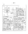
- FIG. 1 shows light emission data by OES (the contents of OES data, particularly the relationship between the light emission spectrum and the waveform).
- the emission intensity spectrum distribution with time on the horizontal axis and wavelength on the vertical axis can be expressed as a bitmap (OES data bitmap) as exemplified by 101-103.
- These bitmaps depict light emission phenomena for a plurality of wafers (light emission intensity gray scale). From the emission intensity spectrum (emission spectrum) 111 at a certain point in time, it can be seen that there is a globally convex shape near the center of the monitor wavelength, and there are peaks at many wavelength positions.
- the emission intensity along the processing time at a specific wavelength that is, the emission intensity changes as the etching process proceeds according to the waveforms 121 and 122, and when the processing content is changed as indicated by the a line in the bitmap 101, It can be seen that the luminescence phenomenon changes.
- the performance of the etching process can be confirmed by monitoring the light emission phenomenon caused by the plasma.
- abnormalities are detected by monitoring light emission during the continuous process of wafers.
- the light emission data is also used as end point detection for determining the end point of the etching process.
- the reason for utilizing the light emission monitor in this way is that light emission is observed at a specific wavelength according to the substance in the chamber. For example, if carbon molecules C 2 473.7,516.5 [nm], if silicon fluoride SiF 334.6,336.3,436.8,440.1,777.0 [nm], also if the nitrogen molecules N 2 282.0,330.9,405.9,580.4,607.0 Emits light at a wavelength such as [nm]. Even for the same molecule, the emission wavelength varies depending on the energy state of the molecule. A peak occurs in the emission spectrum 111 depending on the wavelength of such emission.
- Luminescence intensity Etching is a chemical reaction. A certain substance (molecular structure) is changed to another substance (molecular structure), and these changes are naturally highly correlated.
- FIG. 2 shows the cause of the correlation of the emission intensity based on the reaction (the relationship between the chemical reaction and the waveform).
- the substance [A] is decomposed into the substances [B] and [C], and the reaction process is determined by the formula 202 (primary chemical reaction rate).
- the two substances [A] (2 [A]) become the substance [C], and the reaction process becomes the formula 204 (secondary chemical reaction rate).
- a lot is a unit for starting a wafer.
- One lot is composed of several to tens of wafers, and the wafers are continuously etched in each chamber mounted on the etching apparatus.
- FIG. 3 shows a graph of temporal variation of the emission intensity (uncontrolled emission intensity) at each wavelength for each wafer in the lot-wafer etching process.
- the numbers on the horizontal axis indicate lot units (plots are for each wafer), and the vertical axis indicates the emission intensity and plots for various wavelengths.
- the light emission intensity fluctuates between rising and falling for each wafer in the lot. Variations are also observed between lots.
- the light emission intensity reflects the way of chemical reaction, and this reaction determines the etching performance. Therefore, the fluctuation of the light emission intensity for each lot / wafer means the fluctuation of the etching performance.
- the etching processing conditions are adjusted. That is, various actuators (multiple actuator values) relating to the flow rates of various gases affecting the reaction, currents such as high-frequency power (RF), voltage, pressure in the chamber, and the like are adjusted.
- RF high-frequency power
- Patent Document 1 an apparatus and a processing method for predicting a machining result from a sensor output for monitoring a process amount being processed and adjusting a processing condition so that the machining result becomes a target value. Is shown. In particular, adjusting a plurality of recipe parameters is described.
- Patent Document 2 the film quality of a film to be measured is quantified from the infrared absorption spectrum measured by the FT-IR method (Fourier-transform-Infrared-Spectroscopy), and the film-forming temperature is adjusted. Is described. At this time, PLS regression analysis (Partial Least Square Regression or Projection Latent Structure Regression) is adopted, in which a covariant change of a substance such as a chemical reaction is taken into account.
- FT-IR method Frier-transform-Infrared-Spectroscopy
- Patent Document 3 describes setting processing conditions of a process apparatus in accordance with a processing result that is a measurement result after the process processing.
- a processing result is predicted from operation data of a process apparatus including sensor data such as OES, and that PLS regression analysis is used for this prediction.
- the present invention relates to an etching apparatus having a plurality of actuators for adjusting plasma emission and a device for monitoring plasma emission (such as OES), and adjusts actuator values (corresponding etching processing conditions or recipes) for each wafer process.
- -to-Run control related. This run-to-run control refers to the emission intensities at multiple wavelengths on the emission spectrum during the etching process, so that multiple actuators can achieve the emission intensities at the multiple wavelengths targeted in the next etching process. It was devised for the purpose of calculating values (adjustment amount, control amount).
- control target is a plurality of actuator values (control (adjustment) of the plurality of actuator values corresponds to control (adjustment) of the etching process conditions).
- the purpose of this control is to calculate the adjustment amount (X variation amount ⁇ X) of the actuator set value so that the error from the target value regarding the actual value of the emission intensity (Y variation amount ⁇ Y) is reduced.
- the calculated value (set value) must be within a range (allowable range) that can actually be set in the etching apparatus (actuator). In other words, it is necessary to prevent (limit within an allowable range) the abnormality of the calculated actuator value (X).
- the control performance of the emission intensity (Y) of multiple wavelengths by adjusting the multiple actuator values (X) changes.
- the number of these input / output variables (X, Y) and parameters (A) is large. Therefore, experimental evaluation of control performance in mass production of semiconductor wafers is generally difficult to achieve in the past.
- Patent Documents 1 and 3 describe that the actuator value is calculated from the target value of the inspection result.
- the inspection results include the gate trimming amount, CD (Critical Dimension) value, selection ratio, side etching amount, and taper angle of the CMOS device.
- the relationship between these and the actuator is defined by a response surface model, and the actuator value is determined so as to obtain a target inspection result. That is, each actuator value is determined one by one from a plurality of inspection results. Further, it is shown that the test result is predicted / estimated by, for example, PLS regression analysis using data obtained during operation of an apparatus such as OES.
- a film formation temperature is estimated from an infrared absorption spectrum corresponding to a film quality in film formation, and apparatus setting conditions, that is, actuator values are determined according to the film formation temperature.
- the technical scope is limited to the method for obtaining the actuator value from the sensor data composed of a plurality of data and the inspection result, and the sensor data (light emission intensity) using the model for obtaining the sensor data (light emission intensity) from the actuator value. It does not show how to calculate the actuator value from Furthermore, the problem and the solution method in that case are not shown.
- a main object of the present invention is based on a model (C) for obtaining sensor data, that is, emission intensity values (Y) of a plurality of wavelengths, from a plurality of actuator values (X), and a plurality of emission values (Y) of a plurality of wavelengths. It is to provide a technique capable of calculating an actuator value (X) and realizing a suitable run-to-run control (that is, a suitable etching process) regarding the light emission intensity (Y).
- An object of the present invention is to realize a processing method for determining the suitable parameter (A).
- an emission spectrometer for observing plasma emission (emission intensity of a plurality of wavelengths of emission spectrum) inside the chamber, and a plurality of (for numerical setting) for adjusting the plasma emission
- an actuator for performing an etching process on a wafer. The following is performed in the control function provided in this etching apparatus.
- the value of the parameter (A) included in the control model (C) is set in advance.
- a target value (d3) of the value Y is set in advance.
- (S1) As control of this etching process (Run-to-Run control), (S1) In the first process step, before the start of the wafer etching process, the target value (d3) of the value Y and a plurality of controls are not performed.
- the difference value (d5) between the emission intensity value (d4) and the target control amount (d6) related to the value Y is used, and the value X is calculated from the target control amount (d6) based on the control model (C).
- the control amount (d7) is calculated, and the control amount (d7) is applied as the set value (d1) to the plurality of actuators.
- a predetermined time unit for example, a value Y at a predetermined time point or a value Y within a predetermined processing time range
- the control amount (d7) of the value X calculated in one processing step the plurality of uncontrolled emission intensity values (d4) to be used in the next wafer etching process are calculated.
- the plurality of actuator values X are adjusted by repeatedly executing the first to third processing steps in each wafer etching process (run-to-run control), and the emission intensity values Y of the plurality of wavelengths are obtained. It is characterized by controlling.
- This etching apparatus is equipped with an OES, and the OES is connected to a storage means (DB or the like).
- the etching apparatus stores sensor data (OES data) monitored by OES in the storage means for the plasma emission of the etching process.
- sensor data OES data
- information including a plurality of wavelengths to be controlled and a target value of the emission intensity is used to set the emission intensity at a plurality of predetermined wavelengths as a target value (or approach the target value).
- each actuator (value) can be adjusted (set) in order to control light emission intensities at a plurality of wavelengths according to values of a plurality of actuators provided in the etching apparatus.
- means for setting or instructing an actuator to be used as a control object among a plurality and storing the information in a storage means are provided.
- a control model (C) that defines the relationship between them is required.
- the etching performance depends on the material configuration in the chamber, and the emission intensity at each wavelength varies depending on the configuration. Further, the etching performance is determined by the actuator values, that is, the etching processing conditions related to them. That is, the light emission intensity can be controlled by adjusting the actuator value.
- the relationship of the light emission intensity (Y) to the adjustment amount of the actuator value (X) is determined linearly. That is, the following equation (1).
- x is a vector (change amount) of the actuator value (X)
- y is a vector (change amount) of the light emission intensity value (Y)
- A is a parameter matrix (coefficient matrix).
- the target value (target) (target light emission intensity) of the light emission intensity (Y) is defined as y TGT .
- the actuator value (X) for y TGT can be calculated by the following equation (2).
- control model (matrix model)” etc. because it is a matrix expression (generally, it can be paraphrased as “model by simultaneous equations”) etc.
- the actuator value is calculated from the target emission intensity.
- a means for setting and storing the parameter (A) of the control model (C) based on the matrix model is provided.
- the control model (C) is not limited to the equation (1), and includes means for setting and storing various model definitions.
- a function is provided for calculating an actuator value (X) (adjustment amount) that becomes the target light emission intensity based on the control model (C).
- the light emission intensity (Y) during the etching process is monitored by OES, and the monitor result is used to compensate for variations in the light emission intensity (Y) for each wafer and temporal variations in the light emission intensity (Y) generated by repeated processing. It has a function. With this function, the “emission intensity without control” (the emission intensity without control) at the time of the etching process is obtained, and the adjustment amount of the actuator value (X) can be calculated from the difference from the target emission intensity.
- X actuator set value
- Y emission intensity
- Control simulator In order to evaluate the control result of the emission intensity (Y) of multiple wavelengths according to the set value of the parameter matrix (A) of the control model (C), run-to-run control simulation is performed.
- a control simulator (a predetermined computer system or program connected to or built in the etching apparatus) is used.
- the control simulator has a function of simulating the same calculation as the actual control (actual control, actual etching process) in the etching apparatus. That is, it includes setting and storing means for setting target values, actuator values (X), control models (C), and parameters (A) of emission intensities (Y) of a plurality of wavelengths to be controlled. Also, it has a function of simulating repeated lot start and etching process repeat of multiple wafer starts in a lot.
- a function for calculating an actuator value (X) adjustment amount based on a control model (C) and a function for compensating a temporal variation of light emission intensity (Y) are used.
- Means for generating has a function which calculates the actual value of light emission intensity (Y) by the result of adjusting actuator value (X).
- the actuator value (x) cannot be obtained.
- T on the right shoulder of the vector (same for matrix) means transposition.
- the emission intensity control value (target value and the range considering the upper and lower limits) is [1.5 ⁇ y A ⁇ 2.5], [2.5 ⁇ y B ⁇ 3.5], and the settable actuator value (x: x 1 , x 2 ) is assumed to be [0 ⁇ x 1 ⁇ 2] and [0 ⁇ x 2 ⁇ 2].
- the model is set as the following equation (4) so that the previous parameter matrix (A) is substantially established.
- the actuator value (X) is calculated using two of the matrix model (C1) in which the equation (4) is the parameter matrix (A) and the ratio constraint model (C2) in the equation (5).
- the emission intensity target value [2 3] T is divided (distributed) into two parts, a first target value # 1 [1.98 2.97] T and a second target value # 2 [0.02 0.03] T.
- the first actuator value # 1 [0.310 0.621] T is obtained from the first target value # 1, and from the second target value # 2 based on the matrix model (C1).
- a second actuator value # 2 [1.209 -0.581] T is obtained.
- the actuator set value (X) is [1.520 0.040] T obtained by adding the above two actuator values # 1 and # 2, which is within the setting allowable range of the actuator value (X).
- the control model (C) is defined by an algebraic expression. Therefore, a model for obtaining emission intensity (Y) at multiple wavelengths that is actually generated is defined as a “true control model” (Cb) separately from the control model (Ca) set (applied) by actual control. By repeating the actuator value calculation while calculating the actual light emission intensity, a run-to-run control simulation in the control simulator can be realized.
- Luminescence intensity without control corresponds to the case of assuming no control (no control), obtained by calculation based on the actual value (monitor value) of emission intensity by actual control.
- the light emission intensity (Y) is indicated.
- a plurality of actuator values are calculated from light emission intensity values of a plurality of wavelengths based on a model for obtaining light emission intensity values of a plurality of wavelengths from a plurality of actuator values;
- a suitable run-to-run control i.e., a suitable etching process
- the processing method for the determination of the suitable parameter of the control model (C) for the said control is realizable.
- this control simulation it is possible to reduce the difficulty and real burden of actual work and realize the evaluation and make it efficient and easy.
- (A), (b) is explanatory drawing which shows the basics of run-to-run control in one embodiment of a premise technique and this invention.
- it is explanatory drawing showing contents of two kinds of control models, (a) shows matrix control model (C1), (b) shows ratio restriction control model (C2).
- C1 matrix control model
- C2 ratio restriction control model
- It is a figure which shows the processing flow of Run-to-Run control in the etching apparatus etc. of one embodiment of this invention. It is a figure which shows an example (the 1) of the result (luminescence intensity value) of this Run-to-Run control.
- It is a figure which shows an example (the 2) of the result (luminescence intensity value) of this Run-to-Run control.
- FIG. 6 is an explanatory diagram showing effects and the like in the case where two control models (C1, C2) are integrated (integrated model (C3)) in the etching apparatus and system according to an embodiment (Embodiment 2) of the present invention.
- each actuator value is calculated individually based on the quality after the etching process.
- the adjustment of multiple actuator values affects any quality, that is, the multiple sensor data related to it (light emission intensity of multiple wavelengths)
- the actuator in consideration of the influence on the mutual sensor data (light emission intensity) between the actuators
- the amount of adjustment must be determined.
- the emission intensity of multiple wavelengths which is sensor data monitored by the OES in the etching process, changes the emission intensity at a plurality of wavelengths by adjusting one actuator value.
- This etching apparatus includes a plurality of actuators, OES, and the like, and has a function of run-to-run control of the etching process.
- This control for each wafer start (wafer etching process), a plurality of actuator values X (that is, etching process conditions) are adjusted, and a light emission intensity value Y of a plurality of wavelengths (multiple wavelengths) is controlled.
- Control Model Regarding the relationship (relation model) of the change of the above values (X, Y), first, a control model (matrix) defined by a matrix expression defined so that the value X can be calculated so that the value Y becomes the target value.
- Model: C1 matrix control model: Matrix Control Model
- the relationship between the value Y between a plurality of wavelengths and the relationship between the values X between a plurality of actuators are constrained by a ratio, respectively.
- This is a configuration that can be defined and set in two types: a control model (ratio constraint model: C2) (ratio constraint control model: Ratio-Constraint Control Model) based on a ratio constraint expression that defines a proportional relationship.
- control models (C) According to conditions such as a range (allowable range) in which an instruction (setting) can be actually performed on the actuator (X) and accuracy (Y variation or the like) required for the light emission intensity Y.
- a good control result can be obtained by selecting a model to be applied to the actual control.
- a temporal variation model for compensating (for example, making constant) variation in value Y between lots (multiple lots) and between wafers (multiple wafers) (each embodiment).
- the matrix model (C1) is set when the emission intensity Y (Y actual value) of the control result is set to the target value
- the ratio constraint model (C2) is set when the calculation range of the actuator value X to be set is limited.
- an integrated model (C3) of the two models (C1, C2) is set. The various basic settings can be set by the user.
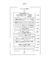
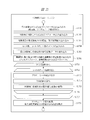
- the etching process is performed once (for each wafer) as follows (FIG. 22).
- the control amount (for this time) of the actuator value X (for this time) (based on the “uncontrolled emission intensity” (d4) or the Y-time variation (d9) d7) is calculated and set to the actuator (X set value (d1)).
- the emission intensity Y (d2) is monitored by OES from the plasma emission based on the actuator setting value (d1), and the data is stored.
- “uncontrolled emission intensity” (d4) is calculated based on the actual Y value (d2) based on the OES data (monitor value / acquired value).
- These processes (S1 to S3) are repeated run-to-run in each etching process. Note that S1 and the like are classifications for convenience of explanation.
- the above configuration can prevent abnormal calculation of the actuator value X or etching processing performance deterioration due to insufficient adjustment of the actuator value X.
- the emission intensity Y the plasma substance composition in the chamber of the etching apparatus can be monitored, so the shape formed depending on multiple substances and the etching amount of films with various compositions can be controlled, and it can be used for LSI miniaturization. Therefore, it is possible to improve the accuracy and to suppress the deterioration of the chamber due to the adhesion of foreign matter.
- the parameter (A) of each of the plurality of models (C) is calculated using the actuator value X and the Y actual value by PLS regression analysis or the like (for example, in the case of the ratio constraint model C2).
- An error between the Y actual value and the estimated value or the predicted value is compared and evaluated, and a suitable control model (C) and parameter (A) are determined from a plurality. The determined one can be set for actual control.
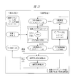
- FIG. 22 shows an outline (image) related to the control (run-to-run control) of the present embodiment (particularly, the first embodiment) as a supplement.
- (D1) and the like indicate symbols for distinguishing various information data.
- E shows an etching apparatus and its etching process. The etching process is in lot-wafer (W) units. For example, the etching process E # i of the wafer W # i of #i this time is assumed.
- the etching apparatus includes a plurality of (J) actuators, OES, and the like as prerequisite technologies.
- the plural (J) actuators or their values are represented by X (individually x), and the emission intensity of the plural (K) wavelengths that can be observed by OES is represented by Y (individually y).
- multiple (j) actuators are selected as targets. These X setting values ⁇ x1, x2,..., Xj ⁇ (d1) are set before the start of the etching process E # i (S1). Plasma emission during the etching process E # i is adjusted by the numerical setting of the plurality of actuators.
- the emission intensity value Y of a plurality of (K) waveforms is monitored by OES and stored for the plasma emission. Based on this OES data, a Y value is acquired in a predetermined time unit to obtain a Y actual value (d2).
- multiple (k) waveforms are selected as targets. Those Y actual values ⁇ y1, y2,..., Yk ⁇ (d2) are used for the calculation.
- the setting of the control model C and its parameters (coefficients) (A), the numbers (j, k) to be targeted (for control) with respect to X and Y, the Y target value (d3 ) And other variables can be set.
- the “setting” here is a user setting that can be made in advance, and has a meaning with the “setting” (for example, the setting of the X setting value (d1)) during the actual control / actual etching process (S1 to S3). Different.
- the control model C can be selected from a matrix model C1, a ratio constraint model C2, an integrated model C3, etc. according to each embodiment (or user setting, function, etc.).
- the parameter (A) and the like can be set in advance. Then, based on the basic setting, first to third processing steps (S1 to S1) constituting repetition of the run-to-run control processing in units of actual control (actual etching processing) (etching processing E for each wafer W). S3).
- the first process step S1 is a process before the current (#i) etching process E # i, and the calculation of the Y target control amount ( ⁇ Y) (d6) from the “uncontrolled emission intensity” (d4), Calculation of X control amount ( ⁇ X) (d7) from ⁇ Y (d6), setting (d1), and the like.
- the second processing step S2 is the execution of the etching process E # i this time (#i), and from the light emission based on the X set value (d1), the Y actual value (d2) is calculated based on the monitor by the OES. obtain.
- the third process step S3 is a process after the current (#i) etching process E # i, such as calculation of “uncontrolled emission intensity” (d4) from the actual Y value (d2). is there. From “Y actual value (d2)”, “uncontrolled emission intensity” (d4), which is “emission intensity without control”, is obtained by calculation (using d3, d7, etc.) (value (d4) obtained in S3) Can be used in S1).
- the difference value (d5) between the “uncontrolled emission intensity” (d4) and the Y target value (d3) is obtained, and this difference value (d5) is used as the Y target control amount ( ⁇ Y). (D6).
- an X control amount (adjustment amount) ( ⁇ X) (d7) is obtained from the Y target control amount ( ⁇ Y) (d6) ( ⁇ Y ⁇ ⁇ X).
- (D4) is calculated.
- a value Y (d2) (monitor value / acquired value) used for calculation is acquired in a predetermined time unit.
- a value at a predetermined time point or a total value for a predetermined processing time range is acquired from the monitor value (Y) by the OES in S2 and set as the value (d2).
- the setting abnormality can be prevented by applying the allowable range related to the X set value (d1) as a condition.
- the temporal variation model (Ct) regarding the value Y is used.
- the Y-time variation amount (d9) is calculated, and based on this, the Y target control amount (d6) is calculated.
- FIGS. 4 and 5 The configuration and operation of an etching apparatus 401 according to an embodiment of the present invention and a system 400 including the same will be described with reference to FIGS. 4 and 5 include components of each embodiment described later.
- 4 mainly shows the configuration of the etching apparatus 401
- FIG. 5 particularly shows the configuration of each function.
- the entire system including the etching apparatus 401 and other elements (432, 433, 434, etc.) is referred to as a system 400 (etching control system).
- an etching apparatus 401 includes a chamber 402, an electrode 403, a wafer 405, an electrode 406, an exhaust system 407, a gas supply system 408, an apparatus controller 409, an OES (emission spectrometer) 410, a computer 411, a screen 412, and a flow rate adjustment.
- the apparatus includes a device 413, a pressure adjustment device 414, a power adjustment device 415, a temperature adjustment device 416, and the like.
- the device controller 409 includes an external communication device and the like.
- the computer 411 is a computer system and includes a storage device and the like, and configures a control function (including a setting function and a run-to-run control function) that is this characteristic element.
- the screen 412 is a means such as a terminal or a display, and includes a user interface (for example, GUI) that facilitates input / output operations by the user.
- a window 421 is provided in the chamber 402, and light 422 (plasma light emission) by plasma can be observed by the OES 410.
- the OES 410 can be regarded as a kind of sensor.
- the etching apparatus 401 is connected to a database (DB) 432 via a network 431.
- DB database
- the network 431 and the DB 432 are also connected to an OES data analysis system 433, a control simulator 434, and the like, which are computer systems.
- the wafer 405 is etched in the chamber 402.
- the wafer 405 is disposed so as to be sandwiched between the electrodes 403 and 406, and the surface of the wafer 405 is etched by generating plasma 404 between the electrodes 403 and 406. Note that the plasma 404 is not necessarily generated by an electrode.
- a gas material necessary for etching is introduced from the gas supply system 408, and the gas after the etching reaction is exhausted from the exhaust system 407.
- the etching apparatus 401 includes a flow rate adjusting device 413, a pressure adjusting device 414, a power adjusting device 415, a temperature adjusting device 416, and the like as a plurality of actuators.
- the pressure, the current / voltage applied to the electrodes 403 and 406, and the temperature can be adjusted. These adjustments (that is, the setting of the actuator value X) are executed in response to an instruction from the device controller 409.
- the plasma 404 is accompanied by light emission, and the light intensity of this light 422 is monitored for each wavelength by the OES 410.
- the OES 410 and the apparatus controller 409 are connected to a computer 411 installed in the etching apparatus 401.
- the apparatus controller 409 has a basic control function of the etching process in the etching apparatus 401.
- the computer 411 performs control to calculate the adjustment amount (control amount) (d7) of each actuator value X based on the emission intensity value Y of each wavelength monitored by the OES 410, and the device controller 409 and the data are obtained. Give and receive.
- the computer 411 stores information data such as the start of each lot and the number and order of etching processes of each wafer in the lot (starting / etching process information), and obtains an adjustment amount of the actuator value X according to the value. To the device controller 409.
- the computer 411 is connected to the screen 412, and the screen 412 displays various information (stored information such as the computer 411 and the DB 432) such as the actuator value X, the light emission intensity value Y, various setting values, and start / etch processing information. Based) to the user (operator, engineer, administrator, control designer, etc.). Further, information that can be set by the user, such as the type (form) and parameter (A) of the control model C required for control, each wavelength of interest, and its Y target value (d3), can be set by the user through the screen 412. The set information is stored in the computer 411, DB 432, etc., and used in this control.
- the OES 410, the apparatus controller 409, the computer 411, and the like in the etching apparatus 401 are connected to the DB 432 via the network 431, store information data in the DB 432, and refer to it as necessary.
- information related to the etching process such as the actuator value X and the wafer processing order can be set by a user operation, and the etching process can be performed by an arbitrary instruction from the user.
- etching processing is performed with various X setting values for each actuator used for control.
- the OES data and the X setting value during the etching process are stored in the DB 432.
- the OES data analysis system 433 conditioning function 521), the user determines the control model C and its parameter (A).
- the OES data analysis system 433 may be implemented as a function of software or the like executed by the computer 411 or the like in the etching apparatus 401.
- Information data stored in the DB 432 includes apparatus log data such as operation data of each actuator in the etching apparatus 401, X setting values (d1) of a plurality of actuators, OES data (monitor data) regarding emission intensity Y of a plurality of wavelengths, and The actual Y value (d2) thus obtained, in particular, the temporal variation data of the emission intensity Y of a plurality of lots and a plurality of wafers is included.
- the setting information includes a plurality (k) of wavelengths to be controlled, a Y target value thereof, and a plurality (j) of actuators.
- the type (form) of the plurality of control models C, parameters (A) thereof, and the like are included.
- it includes information for managing the process and sequence of the lot and wafer etching processing, data on the start history (data obtained from an existing manufacturing management system, etc.), and the like.
- the control simulator 434 evaluates the control result of the light emission intensity Y and the like by fetching data from the DB 432 and executing a run-to-run control simulation. Even if the control simulator 434 is not connected to the network 431, the simulation can be executed by setting data from the terminal of the computer in which the control simulator 434 is installed. Alternatively, the control simulator 434 may be implemented as a function such as software executed by the computer 411 in the etching apparatus 401 or the like.
- the computer 411 (control function) is mounted in the etching apparatus 401.
- a run-to-run control function 501 (components: 502 to 511, etc.) provided in the computer 411 (control function) of the etching apparatus 401, and a condition output function 521 provided in the OES data analysis system 433 are included. (Constituent elements: 522 to 531), and a Run-to-Run control function 501B provided in the control simulator 434 and other functions (541 to 545).
- the emission intensity Y of a plurality of wavelengths is controlled by a plurality of actuator values X for each lot and for each wafer in the lot (Embodiments 1 and 2).
- Embodiment 3), control simulation (Embodiment 4), and the like can be executed.
- the control simulator 434 also has a run-to-run control function 501B, which is a control simulation function corresponding to 501 (for actual control).
- the variation with time of the emission intensity Y is compensated for each lot start and for each wafer etching process in the lot (for example, the value Y is made constant to the target value).
- history information such as the number of wafers processed after apparatus maintenance is acquired from the DB 432 by the lot / wafer etching processing history acquisition function 502.
- the actuator value X is calculated based on the control model C to compensate for fluctuations in the emission intensity Y. Therefore, the control model C and its parameter (A) are set by the control model setting function 503 before the control is performed.
- the target emission wavelength (several k) required for the calculation and the target value (d3) of the emission intensity Y are designated and set by the user using the emission wavelength / emission intensity target value setting function 504,
- the target actuator (number j) to be used for control is designated and set by the user or the like using the control actuator setting function 505.
- the actuator value calculation function 507 uses the control model C to calculate the change amount ⁇ X (X control amount) (d7) of the multiple actuator values X for control. calculate.
- the actuator value command function 508 transmits or commands each actuator value X (X set value (d1)) based on the calculated value (d7) to the device controller 409, and the device controller 409 sends the command to the actuator accordingly.
- the X setting value (d1) is set (applied).
- the current etching process (E # i) (S2) can be started.
- the plasma emission is monitored by the OES 410, the monitor value (OES data) is acquired by the OES data acquisition function 509, and stored in the computer 411. Then, the multiple wavelength emission intensity acquisition function 510 acquires the actual value (d2) of the emission intensity Y of the plurality of (k) wavelengths specified by the setting from the OES data. Since the OES data is waveform data sampled at a predetermined short time interval during the etching process, a data value at a predetermined time unit, that is, a specific time point (interval), or a predetermined process is obtained from the OES data. By obtaining an aggregate value such as an average, maximum, and minimum in the time range, the Y actual value (d2) is obtained.
- the light emission intensity variation with time 511 acquisition function 511 calculates from the above Y actual value (d2) (error (d8) from Y target value (d3)) and X control amount (d7), “Uncontrolled emission intensity” (d4) which is “intensity” is calculated.
- This “uncontrolled emission intensity” (d4) is combined with the temporal variation amount (d9) of the luminous intensity Y generated in the previous wafer etching process to obtain the temporal variation amount (d9) of the luminous intensity Y until now. .
- Y is used to compensate the temporal variation of the emission intensity Y in the next (# i + 1) wafer etching process (E # i + 1).
- the target control amount (d6) can be determined.
- condition output function 521 realized by the processing of the OES data analysis system 433 will be described.
- the condition setting function 521 may be a function realized by a computer 411 in the etching apparatus 401 other than the OES data analysis system 433, for example.
- the actuator level combination setting function 522 sets a value (X) for each actuator as several levels, and sets a combination between the levels of each actuator. Then, wafers corresponding to the number of the level combinations and several wafers for obtaining a standard of temporal variation of the emission intensity Y in the continuous etching process of a plurality of wafers are prepared, and the etching process is actually performed by the etching apparatus 401. carry out. Plasma emission during the etching process is monitored by the OES 410, and the OES data is stored in the DB 432.
- the multiple wavelength emission intensity acquisition function 523 acquires the emission intensity Y of multiple wavelengths (Y actual value (d2)) from the OES data.
- Y actual value (d2) For the target wavelength and the acquisition target time point during the etching process, for example, those specified in the settings are used.
- the light emission intensity Y of the wafer etching process for obtaining the reference for the temporal variation is interpolated in the order of the etching process, and at the time of processing the wafer of the level combination
- the fluctuation ( ⁇ Y) of the light emission intensity Y according to the actuator adjustment amount ( ⁇ X) can be obtained by subtracting the light emission intensity Y from the Y actual value (d2) actually monitored by interpolation / extrapolation.
- the model parameter calculation function 524 for each control model estimates the parameter (A) of the control model C with the emission intensity Y obtained above as an output and the set actuator value X as an input.
- the control model C includes a matrix model C1 and a ratio constraint model C2. Further, since the number of columns of the parameters P and Q can be variably set in the ratio constraint model C2 defined by the equations (5) and (6), there are a plurality of ratio constraint models C2 accordingly.
- the parameter (A) is estimated for each of the plurality of control models C.
- the light emission intensity estimation error calculation / evaluation function 525 substitutes the set actuator value X into each control model C to estimate the light emission intensity Y, and totals the error between the actual value and the estimated value, thereby controlling each control.
- the accuracy of model C can be compared and evaluated.
- the accuracy of the condition determination result can be evaluated by predicting the emission intensity Y.
- the actuator value X for light emission intensity prediction
- the light emission intensity prediction actuator value calculation function 526 is calculated and set by the light emission intensity prediction actuator value calculation function 526.
- the “true control model” (Cb) and its parameter (A) correspond to obtaining the emission intensity Y (Y actual value) in the actual etching process by the “true control model” setting function 527 ( Estimation, setting, etc.).
- the emission intensity calculation / evaluation function 528 calculates the emission intensity Y using the actuator value X based on each control model C in which the “true control model” (Cb) and its parameter (A) are estimated, and the comparison is made. Can be evaluated.
- information such as the Y target value (d3) is acquired from the DB 432 by the multi-wavelength emission intensity target value acquisition function 529.
- the multi-wavelength emission intensity control amount calculation function 530 calculates the difference between the emission intensity Y calculated from the actuator value X based on the “true control model” (Cb) and the Y target value (d3) as the Y control amount ( d6).
- the actuator value calculation / evaluation function 531 calculates the actuator value X (control amount (d7)) using the Y control amount (d6) based on each control model C in which the parameter (A) is estimated. Thereby, the actuator fluctuation amount can be compared and evaluated for each control model C.
- the Y control amount (d6) is calculated from the control model C, the parameter (A), the actuator value X, and the like by the non-control light emission fluctuation calculation function 545, and subtracted from the light emission intensity value Y. Emission intensity fluctuation data is obtained.
- the actuator value X (control amount) is calculated by the actuator value calculation function 507 with reference to the Y variation with time until the previous time. Then, a calculation process (simulation) corresponding to the execution of the actual etching process (S2) is performed.
- the multi-wavelength emission intensity calculation function 542 calculates a Y control amount using the actuator value X based on the “true control model” (Cb), and adds “true emission intensity without control” to the emission intensity. A control result (simulation result) of Y is obtained.
- This emission intensity Y is regarded as the emission intensity (Y actual value) monitored by the OES 410, and the Y intensity variation amount is obtained by the emission intensity variation amount acquisition function 511 as in the case of the run-to-run control function 501. .
- the Y control amount subtracted from the light emission intensity Y at this time is calculated when the actuator value X is calculated, and is not a Y control amount based on the “true control model” (Cb).
- emission intensity (Y) 642 having a plurality of (K) wavelengths is acquired from the OES data of plasma emission 641 monitored in Step 2 (Process 631). Then, before starting the etching process E # i + 1 of the next i + 1-th wafer W # i + 1 shown on the right side, the light emission intensity (Y) 642 is referred to based on the control model (many-to-many related control model) 632, and the light emission intensity A plurality of actuator values (X) 643 are calculated so that the value Y becomes the target value (d3).
- the actuator value (X) 643 is set in a recipe such as “recipe item 1”, “recipe item 2”,.
- the recipe is an etching process condition including a plurality of items. Since the actuator value X, the etching process condition (recipe), and the elements (one or more of each) such as the etching step have a predetermined relationship, the direct control target is a plurality of actuators (X).
- the etching process E # i + 1 of the wafer W # i + 1 is started.
- the actuator 644 one related item
- the actuator 644 operates from the value of “recipe item 4” in Step 3 and from the value of “recipe item 5” in Step 4, respectively.
- actuator values (X) 643 based on the control model (many-to-many related control model) 632, as shown in FIG. A many-to-many numerical relationship with the axis as the actuator value X must be established.
- the control model C is defined in two ways: a matrix model C1 and a ratio constraint model C2.
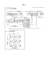
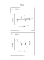
- Control model> The contents of this control model (C: C1, C2) will be described with reference to FIG. (A) is a graph of the matrix model C1, and (b) is a graph of the ratio constraint model C2.
- the graph shows an emission spectrum in which the horizontal axis is the wavelength and the vertical axis is the emission intensity Y.
- the emission intensity Y of the two wavelengths (A, B) is 2 This is an example of controlling with actuators (# 1, # 2).
- the matrix model C1 in FIG. 7A can be defined based on the fact that each of the plurality of actuators can control the emission intensity Y of each wavelength to a target value.
- the wavelengths to be controlled are the wavelength A and the wavelength B, and the Y target control amount (d6) that is the difference (d5) between the Y target value (d3) and the “uncontrolled emission intensity” (d4) is y A (706) and y B (707) at the wavelength B.
- the actuator # 1 (its control amount) (708) is adjusted, the emission intensity Y of both wavelengths A and B changes, but when the actuator # 2 (its control amount) (709) is adjusted, the emission intensity of the wavelength B is adjusted. Only Y changes.
- the actuator # 1 (708) is adjusted to the control amount y A (706), and the control amount y B (707) cannot be controlled by the actuator # 1 (708). May be controlled by actuator # 2 (709). That is, the actuator value X can be obtained so that the target control amount can be obtained.
- the matrix model C1 is expressed by equation (7), and the calculation formula for the actuator value X is expressed by equation (8).
- a y T [y A y B ... y Char (N)] T
- x T [x 1 x 2 ... x M] T
- N is the number of wavelengths (or the number of sensors) (corresponding to the aforementioned numbers k and K)
- Char (i) means the i-th capital letter.
- the parameter A is expressed by the following equation (9).
- This parameter A can be obtained by multiple regression analysis (in the case of C1).
- the ratio constraint model C2 in FIG. 7B can be defined based on the fact that the emission intensity Y of each wavelength changes at a constant ratio by adjusting each actuator value X.
- the actuator # 1 (its control amount) (718) is adjusted, the emission intensity Y of both wavelengths A and B changes, and even when the actuator # 2 (its control amount) (719) is adjusted, the wavelengths A, B Both the emission intensities Y of B change.
- the change amount ⁇ Y of the value Y at each wavelength is a constant ratio for each actuator. Therefore, the actuator adjustment amount ( ⁇ X) is obtained so as to be as close as possible to the two Y target control amounts.
- the ratio constraint model C2 is expressed by the following equations (10) and (11).
- internal variable t [t 1 t 2 ... T L ], and L is called the number of internal models.
- the parameter P is a matrix of M rows and L columns
- P [p 1 p 2 ... P L ]
- p i T [p 1i p 2i ... P Mi ]
- the parameter Q is a matrix of N rows and L columns.
- Q [q 1 q 2 ... Q L ]
- q i T [q 1i q 2i ... Q Ni ].
- the lower right subscript i is the number of the internal model.
- the number of actuators M and the number of wavelengths N may be different (in the case of C2). However, L is less than min ⁇ N, M ⁇ . min ⁇ a, b ⁇ is an operation for selecting the smaller number of a and b.
- the parameters P, Q, and B can be obtained by PLS regression analysis. Note that x is an input (corresponding to X), y is an output (corresponding to Y), an internal variable t is called a score, and parameters P and Q are called loading.
- the internal variable t is deleted from the equations (10) and (11), the following equations (12) and (13) are obtained. That is, the internal variable t is not particularly necessary for estimating the emission intensity Y or calculating the actuator value X.
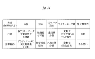
- FIG. 14 shows a comparison table of the above two control models C.
- the matrix model C1 individual light emission is controlled by each actuator as a feature. Fine tuning is possible as an aim.
- Parameter setting is based on multiple regression analysis.
- the control amount is distributed to the actuator as a feature.
- the goal is chemical reaction orientation.
- the parameter setting is based on PLS regression analysis.
- the Y tabulation method is, as described above, an acquired value in a predetermined time unit based on the OES data, for example, 20 seconds from the start of the etching step process, or This is a method for obtaining the light emission intensity value Y from OES data such as an average of 30 to 40 seconds.
- the wavelength can be selected based on an assumed chemical reaction.
- the wavelength may be determined by automatically detecting a peak on the emission spectrum based on a threshold value or the degree of unevenness. Further, whether or not the emission intensity Y varies with time may be determined by observing the OES data. Alternatively, if the waveform during the etching process (the emission intensity with respect to the processing time) is observed and a waveform having a large change greatly contributes to the chemical reaction, the wavelength of the waveform can be selected. Further, by determining the similarity of the waveform shapes at a plurality of wavelengths, for example, by determining that the waveforms that are similar to each other are light emission caused by the same substance, the wavelengths can be selected.
- the Y target value (d3) can be determined with reference to, for example, the emission intensity value Y generated by the etching process under the etching process conditions (recipe, etc.) determined as a standard. Or, by combining the inspection results of wafers that have been actually etched, such as CD dimensions and gate / wiring aspect ratio, with OES data, and building a relationship model between the inspection results and emission intensity Y, the desired inspection results can be obtained.
- the emission intensity Y can be determined.
- a management value of the emission intensity Y may be set in order to manage the etching repeatability.
- etching is a chemical reaction
- the amount of a substance in the chamber 402 can be adjusted by introducing a specific gas, and the reaction rate can be adjusted by pressure or temperature.
- the ionization state of the plasma 404 is determined by the electromagnetic state in the chamber 402, it can be adjusted by a related actuator such as electric power.
- Each actuator value (X) has a substantial physical limit (setting allowable range) such as a flow rate adjustment range depending on the type of the actuator. There is also the danger of accidents by increasing the response. Therefore, in consideration of these, a predetermined set value such as an upper limit or a lower limit may be set for the actuator value X (d1) and applied as a condition to the main control.
- control model C and its parameters (A) are set.
- the control model C can be selected from the matrix model C1 and the ratio constraint model C2. In the case of the ratio constraint model C2, the number of internal models (L) is also set.
- the parameter (A) is A in Equation (7) for the matrix model C1, and P, Q, and B in Equation (12) for the ratio constraint model C2.
- the parameter (A) value can be determined by setting conditions.
- the parameter (A) may be obtained by multiple regression analysis or PLS regression analysis based on a plurality of samples of the light emission intensity Y monitored by the variously set actuator value X and the OES 410 during the actual etching process.
- the parameter (A) of the model (Y time variation model Ct) is also set. Keep it.
- parameters for the algorithm are also set.
- the etching apparatus 401 is maintained, and the etching performance of the apparatus is confirmed by trial etching.
- the emission intensity Y is monitored by the OES 410, the initial value of the emission intensity Y of the wavelength to be controlled is obtained.
- a reference value (standard value, representative value, etc.) is set for the actuator value X.
- the emission intensity Y obtained here is the initial value y No * [0] [0] of “uncontrolled emission intensity” (d4).
- an asterisk “*” means an actual value.
- a container (cassette, FOUP (Front Opening Unified Unified Pod)) corresponding to a lot storing a plurality of wafers is installed in the etching apparatus 401.
- the wafer may be directly stored in the etching apparatus 401, may be manually installed, or may be automatically installed (distributed, recovered) using an automatic transfer apparatus or the like.
- the control model C includes a difference (d5) between the “uncontrolled emission intensity” (d4) and the Y target value (d3), that is, the Y target control amount (d6), and the actuator value X (X control amount (d7)).
- This is a relationship model.
- the actuator value X ( ⁇ X) the “uncontrolled emission intensity” y No [#ii] [# jj] when performing the etching process is required.
- This value may be a calculated value of “uncontrolled emission intensity” (d4) in S810 in the previous control of the wafer etching process, but is calculated using a temporal variation model (Ct) of “uncontrolled emission intensity”. It is good also as a value to be done.
- Expression (14) is an example of a temporal variation model (Ct).
- Drift lot is the aging fluctuation gain for every wafer
- Drift wafer is the aging fluctuation gain for each wafer in the lot.
- the actuator value X (x) can be calculated by the equation (8) if the matrix model C1 and by the equation (13) if the ratio constraint model C2.
- the Y control amount is obtained by the equation (7) for the matrix model C1 and by the equation (12) for the ratio constraint model C2, and this is calculated as the set control amount y set [#ii]. [#jj].
- the set control amount (corresponding to the Y target control amount (d6)) is used.
- the actual etching process is started by the etching apparatus 401.
- the actuator operates according to the actuator value X (X set value (d1)) calculated in S807.
- Plasma emission during the etching process is monitored by the OES 410 and the OES data is stored.
- step S809 the emission intensity Y (Y actual value (d2)) (acquired value in a predetermined time unit) of the designated target wavelength is acquired from the OES data.
- the calculation of the wavelength, the etching step, and the emission intensity value Y at this time may follow the setting in S801.
- the emission intensity y * [# ii] [# jj] obtained here is referred to as a Y actual value (d2).
- the “actual value of uncontrolled emission intensity” may be directly used as “uncontrolled emission intensity” (d4) for calculating the actuator value X in the next wafer etching process.
- a filter may be used to remove noise and smooth the fluctuation over time.
- EWMA Extraly-Weighted Moving Average
- the parameter (A) of the time variation model (Ct) may be updated.
- the above is the processing content of the run-to-run control based on the matrix model C1 or the ratio constraint model C2 in the first embodiment.
- the semiconductor device manufacturing method of the present embodiment realized by using the etching apparatus 401 and the system 400 of the present embodiment is as follows.
- a lot and wafer etching process in a known semiconductor device manufacturing method is performed by an etching apparatus 401 and its system 400.
- a plurality of lots that have been subjected to the exposure process before the etching process are installed in the etching apparatus 401.
- a lot is automatically distributed from the production line to the etching apparatus 401 on a predetermined schedule using an automatic transfer device, and the lot after the etching process is collected to the production line.
- the above-described etching process in units of lots and wafers is continuously and repeatedly executed.
- each wafer 405 is continuously etched in the chamber 402.
- run-to-run control based on the basic settings is automatically performed by the computer 411 (control function) described above.
- the light emission intensity Y of the lot and wafer as shown in FIG.
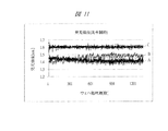
- FIGS. 9 to 13 show example results of run-to-run control based on the matrix model C1 and the ratio constraint model C2. This is a case of controlling 3 wavelengths (3 sensors) -3 actuators.
- 9 to 11 show graphs of the temporal variation of the light emission intensity Y (actual value for each wafer)
- FIG. 9 shows the light emission intensity without control
- FIG. 10 shows the light emission intensity in the control based on the matrix model C1
- the emission intensity Y of wavelength A (target value 1.4) is indicated by a solid line
- Y of wavelength B (target value 1.5) is indicated by a dotted line
- Y of wavelength C (target value 1.6) is indicated by a broken line.
- 12 and 13 show graphs of fluctuations in the actuator value X.
- FIG. 12 is a graph of X fluctuations in the control based on the matrix model C1
- FIG. 13 is a graph of X fluctuations in the control based on the ratio constraint model C2. is there.
- the first actuator value (x 1 ) is indicated by a solid line
- the second actuator value (x 2 ) is indicated by a dotted line
- the third actuator value (x 3 ) is indicated by a broken line.
- the horizontal axis represents the wafer processing order [sheets]
- the vertical axis represents the emission intensity Y [au] in FIGS. 9 to 11, and the actuator value X [au] in FIGS. .
- a numerical value is added to the scale on the vertical axis, but this is to show that the scale is equally spaced, and the absolute value itself is irrelevant to the actual etching process.
- the wavelength A greatly decreases from about 1.7 to 1.2.
- the wavelength A, the wavelength B, and the wavelength C vary in white noise, but the average is a target value.
- the control emission intensity Y based on the ratio constraint model C2 in FIG. This change is because the actuator value X cannot be calculated so that the control amount matches the target value in the ratio constraint model C2.
- the variation in the light emission intensity Y is smaller than that in the case where the control is not performed, and approaches the target value.
- the first actuator value (x 1 ) greatly increased from ⁇ 0.1 to 0.1.
- the variation range of the values (x 1 , x 12 , x 3 ) is within a range of ⁇ 0.3.
- Fig. 14 shows the above relationship in an organized manner.
- the actuator value X varies greatly (there is a risk of rank drop), but the controllability (emission controllability) of the emission intensity Y is good.
- the actuator value X varies little (easy to set), but the light emission controllability is somewhat poor. That is, when the control is performed based on one of the control models, a problem occurs in the setting of the actuator value X depending on the accuracy of the required etching processing result or the limit (allowable range) of setting to the actuator. Alternatively, there is a possibility that the accuracy will be insufficient by deviating from the range that the emission intensity Y satisfies.
- the variation amount of the emission intensity Y is reduced (control target) while the adjustment amount of the actuator value X is kept within a narrow range.
- the two control models (C1, C2) are integrated in view of the characteristics of the fluctuation of the actuator value X and the light emission intensity Y in the run-to-run control based on the matrix model C1 and the ratio constraint model C2.
- This matrix + ratio constraint integrated control model is defined as an integrated model C3.
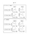
- FIG. 15A shows the effect of temporal variation of the actuator value X due to the integration of the models.
- the adjustment range of the value X shown in a is large and cannot be set.
- the adjustment range of the value X is small.
- FIG. 15 (b) shows the effect of temporal variation of the emission intensity Y by model integration.
- the value Y has a small fluctuation.
- the temporal variation graph of the light emission intensity Y in the run-to-run control based on the ratio constraint model C2 shown in (b2) the value Y is very large as shown by b. Since the control amount of the light emission intensity Y is distributed to each model in the calculation of the actuator value X, the fluctuation of the light emission intensity Y is reduced by the amount of the control amount assigned to the matrix model C1.
- the value Y becomes small as shown by c, that is, the accuracy of the etching processing result is improved.
- the integrated model C3 is defined by the following expressions (21) and (22).
- Equation (21) is a distribution constraint.
- the distribution coefficient can be a vector.
- the first and second stages of the equation (21), the equation (22) is changed to the following expressions (the equations (23) and (24)).
- D is a distribution coefficient vector having the number of emission wavelengths N as the number of elements. Since a vector comprising the weights with respect to the emission intensity Y, the diagonal elements of the matrix is the product of the column vector D and the horizontal vector y T can be expressed Taking.
- diag (M) is an operation that makes the diagonal elements of the square matrix M a vertical vector, and the content of the operation is different from the case where a scalar array or a vector is used as an argument.
- the distribution coefficient D MAT , D RC or the distribution coefficient vector D MAT , D RC is set in addition to the other setting items.
- the calculation method of the value X is different.
- the value X is calculated based on the control model C (C3), with the difference (d5) between the Y target value (d3) and the non-control emission intensity (d4) as the Y target control amount (d6).
- the Y target control amount y is distributed to the first control amount based on the matrix model C1 and the second control amount based on the ratio constraint model C2. That is, the following expressions (25) and (26).
- the actuator value X (first value X, second value X) is calculated separately for each model (C1, C2) and added to obtain the calculated value of the actuator value X. That is, the following equations (27), (28), (29).
- the set control amount y set [#ii] [# jj] is calculated by equation (21) or equation (23). The above is the processing content of the run-to-run control based on the integrated model C3.
- ⁇ Rank drop> There are other concerns about the matrix model C1. As shown in FIG. 8, in calculating the actuator value X for the matrix model C1, there is a risk that it cannot be calculated due to a rank drop. If the parameter (A) is used in the condition setting, the actual Y value varies, so the parameter (A) of the matrix model C1 can be calculated so as not to drop the rank. Therefore, the calculated value of the actuator value X is abnormal. Value. Therefore, the condition for dropping the rank is that the determinant
- ⁇ det is an uncontrollable determination upper limit value.
- abs is an operation that takes an absolute value.
- the actuator value X may be calculated according to Equation (8), and it may be determined whether or not control is possible based on the calculated X value. Now, it is assumed that the parameter (A) of the matrix model C1 of the following equation (31) is obtained by condition setting.
- the actuator value X By calculating the actuator value X by setting the control amount of the emission intensity Y to the parameter (A) of the matrix model C1 obtained in this way, it can be determined whether or not the control can be performed using the matrix model C1. .
- the standard actuator value X is ⁇ 10 or more and +10 or less (range)
- the absolute value of the element of the inverse matrix is large, so the determination may be made by the value of the inverse matrix. If the matrix is modified by basic transformation and parameter A is transformed so that all one row and one column are all 1, then it is determined whether all the values are 1 in other rows or columns. You can find the wavelength or actuator that causes the drop.
- a T P a Q T and make it coincide with P (P T P) ⁇ 1 BQ T.
- B is a unit matrix.
- the parameters (A) B, Q, and P of the ratio constraint model C2 are set as in the following equations (33), (34), and (35).
- the parameters (A) B, Q, and P of the ratio constraint model C2 are set as in the following equations (37), (38), and (39).
- the parameter (A) of the ratio constraint model C2 can be obtained from the matrix model C1 by using PLS regression analysis.
- the input of the matrix model C1 is appropriately set to calculate the output, and a large number of samples are created. If PLS regression analysis is performed using the sample, B, Q, and P, which are parameters of the ratio constraint model C2, can be obtained. New condition setting work is unnecessary.
- the etching apparatus 401 according to the third embodiment will be described with reference to FIGS.
- a processing method for determining conditions for determining the matrix model C1 and the ratio constraint model C2 and their parameters (A) will be described.
- the condition setting method itself in the third embodiment is configured based on a known design of experiments (DOE). That is, each actuator value X is set to a level of several steps, and etching is performed by combining the levels of each value X, thereby obtaining the fluctuation amount ( ⁇ Y) of the emission intensity Y with respect to the adjustment amount ( ⁇ X) of the actuator value X. Is the method.
- DOE design of experiments
- the first few wafers in the lot are processed, and subsequent wafers are etched with an X adjustment amount according to the level assignment by the experimental design method, and the value Y is monitored by OES.
- the parameter (A) of the time variation model (Ct) of the value Y is estimated from the first few results, and the variation amount (sample) of the value Y corresponding to the adjustment amount of the value X is obtained from the subsequent wafer results. Is used to calculate the parameter (A) of the control model.
- the feature of the third embodiment is that the conditions for obtaining the above two models (C1, C2) are determined, that the actual Y value, that is, the sample value is determined by compensating for the variation over time in the etching process. For example, the number of etching processes and the number of wafers may be reduced in order to reduce the number of man-hours required for determining the conditions.
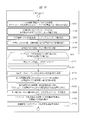
- condition setting process The contents of the condition setting process will be described according to the flow of FIG.
- a thick frame part (S1201 and the like) is a manual (user) setting process, and the other part is a process by the etching apparatus 401 or its computer 411 or the like.
- the condition determination function 521 is implemented in the OES data analysis system 433, but here the function (521) is implemented in the etching apparatus 401 and subjected to calculation processing by the computer 411. This will be described as a form.
- the etching process may be performed by the etching apparatus 401
- the setting and calculation processes may be performed by the OES data analysis system 433.
- an intra-lot time variation model (referred to as Ct1) is set, and the number of etching processes (number of wafers) (referred to as w2) by an actuator representative value (referred to as Xr) is set.
- the intra-lot time variation model (Ct1) is a representation of the variation in the light emission intensity Y that occurs when the wafers in the lot are continuously etched one by one. This is an example of an expression obtained by eliminating one item on the right side in Expression (14).
- the actuator representative value (Xr) is the actuator value X to which the adjustment amount (control amount) (d7) is not added, that is, “actuator (value) setting without control”.
- the horizontal axis of the graph is the wafer processing order [sheets] under conditions, and the vertical axis is the emission intensity Y.
- the black circle plot represents the emission intensity Y in the etching process with the actuator representative value (Xr), and the white circle plot represents the emission intensity Y in the etching process with the actuator level combination. It is assumed that the emission intensity Y increases at a constant rate in the etching process order. In this case, it is necessary to quantify the control amount (change amount ⁇ Y of the light emission intensity Y) by the actuator level combination and the change amount ⁇ Y of the light emission intensity Y by the repeated etching process.
- an estimated line indicated by a which is a tendency of temporal variation is obtained from the light emission intensity Y (black circle) in the etching process with the actuator representative value (Xr). Then, if the difference between the light emission intensity Y (white circle) and the estimated line (a) in the etching process with the actuator level combination is taken, it is the change amount ⁇ Y of the light emission intensity Y by the level combination, that is, the control amount. For example, the difference between the emission intensity Y and the estimated line (a) at the level combination indicated by b is the control amount indicated by c.
- the estimated line (a) is obtained by determining the parameter (A) based on the actual Y value at the actuator representative value (Xr) after setting the intra-lot variation model (Ct1) as a straight line, and the emission intensity without control. It becomes a line which means the change for every etching process.
- the etching process using the intra-lot time variation model (Ct1) and the actuator representative value (Xr) is required. Become.
- the intra-lot time variation model (Ct1) may not be a straight line but may be a nonlinear expression such as a quadratic expression.
- the number of etching processes using the actuator representative value (Xr) must be equal to or greater than the number of parameters when the parameter (A) is determined using multiple regression analysis, for example. If one of the actuator level combinations is the actuator representative value (Xr), the number of processes may be reduced by one. If there is no variation with time in the lot, the etching process using the actuator representative value (Xr) may be performed once, and the difference between the emission intensity Y and the emission intensity Y at each level combination is the control amount.
- the actuator used for control is specified, and the number of levels and the value X at each level are set.
- an actuator that is expected to change the light emission intensity Y is selected.
- the number of levels is 2 levels if the value is set to 2 levels, 3 levels if the level is set, and the actuator value X at each level is a physically acceptable range or a predetermined etching performance. It may be set based on the allowable range. For example, when the allowable setting range of the actuator value X is -15 to +15, and the third level is set, the first level actuator value is -10, the second level value is 0, and the third level value is +10. do it.
- the setting content may be stored in a file or DB 432 and read by the computer 411. .
- the etching apparatus 401 Based on the set information, the etching apparatus 401 generates a level combination and presents a candidate for the level combination to be experimented to the user who is performing the condition setting. This presentation may be in the form of displaying information on the screen 412, for example.
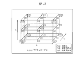
- FIG. 18 is a diagram representing all actuator level combinations as a grid when three levels of value X are set for three actuators.
- Such a level combination setting method is called orthogonal arrangement, and the number of level combinations is generally M to the power of q (M q ), where M is the number of actuators and q is the number of levels.
- Numerical symbols (111, 211,..., 122, 222,..., 233, 333) attached to the grid (nodes) in FIG. 18 represent level combinations, and the first number is the first number.
- level of the actuator values x 1 the second number is the second actuator value x 2
- 3 nd numbers means the level of the third actuator value x 3.
- the parameter (A) in the matrix model C1 is to obtain the parameter (A) for each wavelength based on the relationship of the change in the emission intensity Y of the three wavelengths with respect to the three actuators. Therefore, the parameter (A) can be calculated with at least three samples, and in order to calculate the variation (standard deviation) of the emission intensity Y, four samples are sufficient. If the number of internal models (L) is 1 for the ratio constraint model C2, the parameter (A) can be calculated by NIPALS (NonNlinear Iterative PArtial Least Squares) in one sample.
- NIPALS NonNlinear Iterative PArtial Least Squares
- each actuator value X covers all levels, that is, if the level is 3, the levels 1, 2 and 3 are set for any actuator.
- the user is presented with 27 level combinations, 9 level combinations, and 4 level combinations, and an arbitrary level combination can be selected.
- the user selects a level combination and sets the number of wafers (w3).
- the level combination is set in consideration of, for example, the number of available wafers, particularly the actuator to be examined in detail. Further, when it is desired to evaluate the variation in the light emission intensity Y at the same actuator value X rather than the change in the light emission intensity Y according to the setting between the levels of the actuator value X, for example, the number of wafers at each level combination is two, three You just have to do it.
- the emission intensity Y (Y actual value) of the specified wavelength is acquired from the OES data in S1221.
- the emission intensity Y is acquired according to the etching step designated in S1203, the Y counting method, and the like.
- the parameter (A) of the intra-lot time variation model (Ct1) is obtained, and the uncontrolled emission intensity during the level combination etching process is estimated.
- the intra-lot variation model (Ct1) is expressed by the following equation (42).
- #jj is the number of processes from the first wafer in which S1211 to S1213 are repeated.
- the coefficients are Drift and Shift. If two wafers are now etched using the actuator representative value (Xr) and the emission intensity Y (sample) at that time is y Sample * [1], y Sample * [2], Drift and Shift are It is obtained as shown in equations (43, 44).
- the intra-lot time variation model (Ct1) may be higher than second order. Further, the number of parameters (A) in the intra-lot time variation model (Ct1) may be larger than that of the actuator representative value (Xr), and the parameter (A) may be estimated by multiple regression analysis.
- the non-controlled emission intensity is subtracted from the emission intensity Y, and the actual value of the fluctuation amount ⁇ Y of the emission intensity Y with respect to the actuator level combination, that is, the control amount is calculated. If the number of etching processes (w2) based on the actuator representative value (Xr) is N No , the actual value of the fluctuation amount ⁇ Y is obtained by the following equation (45).
- the subscript DOE is for clearly indicating that the actual value of the fluctuation amount ⁇ Y obtained by setting the conditions.
- #comb is the number of levels combined is the number of 1 ⁇ N comb.
- N comb is the number of actuator level combinations.
- the parameter (A, C2) of each control model (C1, C2) is obtained by using the condition calculation actual sample (x DOE * [#comb], y DOE * [#comb]) by multiple regression analysis or PLS regression analysis. ).
- a which is a parameter of the matrix model C1 is obtained by the following equations (46), (47) and (48).
- NIPALS (X, Y, L) is a function that returns P, Q, B, and the arguments are input sample (X), output sample (Y), and number of internal models (L).
- L which is the number of internal models, ranges from 1 (the minimum number of internal models) to a smaller number (min ⁇ M, N ⁇ ) of the number of actuators M and the number of wavelengths N (1 ⁇ L ⁇ min ⁇ M, N ⁇ ).
- the light emission intensity Y is estimated using the actuator level combination, and the error from the actual value is totaled.
- This error e is obtained from the difference between the actual value of the light emission intensity Y and the estimated value as in the following equation (50).
- the hat “ ⁇ ” means an estimated value.
- the estimation based on the matrix model C1 can be calculated by the equation (51), and the estimation based on the ratio constraint model C2 can be calculated by the equation (52).
- the average value and standard deviation are calculated. If the average is a large value, the estimation result by the model is larger than the actual value, and if the standard deviation is large, the estimation error by the model is more varied. In any case, the closer to zero, the higher the estimation accuracy of the model.
- control models (C1, C2) by predicting the emission intensity Y is also possible.
- the condition actual results samples (sample number N comb ) of all actuator level combinations are now divided into model parameter calculation samples (sample number N reg ) and prediction samples (sample number N pred ).
- N comb N reg + N pred .
- the parameter (A) is calculated based on the equation (49) using the parameter calculation sample.
- the calculated parameter (A) is set as a “true model parameter”, the prediction value of the light emission intensity Y is calculated by the equation (52) using the prediction sample, and the prediction error is calculated based on the equation (50).
- the control models (C1, C2) can be compared and evaluated.
- N comb in equations (47) and (48) is N reg
- #comb in equations (50) and (52) is interpreted as an index of a prediction sample
- an estimated value is interpreted as a predicted value.
- the number of etching processes (w2) by the actuator representative value (Xr) is 1, and 0 if the actuator representative value (Xr) exists in the actuator level combination. If there is intra-lot variation over time, the variation can be approximated linearly, and the number of processes (w2) is 2, and if there is an actuator representative value (Xr) in the actuator level combination, it is 1. Therefore, the number of processes (w2) based on the actuator representative value (Xr) is determined by one of 0, 1, and 2.
- the number of samples must be greater than the number of internal models (L).
- the number of internal models (L) can be in the range of 1 (minimum number of internal models) to min ⁇ M, N ⁇ (maximum number of internal models) (arbitrary within that range).
- the light emission intensity Y of a plurality of wavelengths is controlled by the actuator value X.
- the number of wavelengths (N) or less is used in the control.
- the number of actuators (M) is set (N ⁇ M).
- the number of samples for determining the parameter (A) of the control model C is determined from the above internal model minimum number (1) to the number of actuators (M) (1 ⁇ number of samples ⁇ M). .
- M the number of actuators
- the minimum number of wafers required for determining the condition is the number obtained by adding 1 for variation evaluation to 0 or less actuators (M) used for control, and adding 0, 1 or 2 for compensation for variation over time. Become.
- FIG. 19 illustrates these cases.
- FIG. 19 shows an example of (a) actuator invalidity and (b) wavelength invalidity.
- Two actuators (# 1, # 2) are arranged in the row direction, two wavelengths (A, B) are arranged in the column direction, and a graph is arranged with the actuator value X on the horizontal axis and the emission intensity Y on the vertical axis. .
- the plot in the graph is the light emission intensity Y for each level of the actuator.
- the emission intensity Y increases at wavelength A as indicated by c, and the emission intensity Y decreases at wavelength B as indicated by d. To do. Therefore, the emission intensity Y can be controlled by the second actuator # 2.
- the first actuator # 1 does not have a clear tendency to rise or fall like the emission intensity Y at the wavelength A indicated by a and the emission intensity Y at the wavelength B indicated by b. Since both the matrix model C1 and the ratio constraint model C2 have a proportional relationship between the emission intensity Y of one wavelength with respect to one actuator, the emission intensity Y of these wavelengths cannot be controlled by the first actuator # 1.
- the emission intensity Y decreases as indicated by a, and when the second actuator # 2 is adjusted, as indicated by c. Further, since the emission intensity Y increases, it can be controlled.
- the light emission intensity Y indicated by b and the light emission intensity Y indicated by d are respectively adjusted by the first actuator # 1 and the second actuator # 2, and cannot be controlled.
- the corresponding actuator is not used for control, or the corresponding wavelength is excluded from the control target.
- the actuator value X is plotted with the horizontal axis, the emission intensity Y with the vertical axis, and the Y actual value with white circles.
- the broken line a is an estimated line of the emission intensity Y by multiple regression analysis using a plot.
- A When there is no change, the change amount ⁇ 1 of the light emission intensity Y in the adjustment range of the actuator value X is smaller than the error e between the actual value and the estimated line a.
- the amount of change ⁇ 2 of the emission intensity Y is larger than the error.
- the presence / absence of variation can be determined by ⁇ / ⁇ . If ⁇ / ⁇ is smaller than a reference value, for example, 3, it may be determined that the emission intensity Y does not vary.
- the etching apparatus 401 according to the fourth embodiment will be described with reference to FIG.
- the control performance when the light emission intensity Y of a plurality of wavelengths is run-to-run controlled by the plurality of actuator values X that is, the error of the control result light emission intensity Y (Y actual value) with respect to the Y target value is realized.
- a control simulation for evaluating without performing an etching process will be described.
- the control model C for calculating the Y actual value is defined as “true control model” (Cb)
- the control model C for calculating the actuator value X is the control model (Ca) set for control.
- the control model (Ca) for control is also used for compensating the temporal variation of the emission intensity without control. This control model (Ca) for control corresponds to the control model C set and used in actual control (actual run-to-run control).
- Control simulation-process flow The processing contents of the control simulation by the control simulator 434 will be described according to the flow of FIG. The contents of this process are all executed by the control simulator 434 (its computer system).
- the “true control model” (Cb) and the parameter (A) of the control model C are read.
- the definition itself of the control model C includes the input wavelength number (N) and actuator number (M). However, in the simulation, information such as wavelength [nm] information and actuator type is unnecessary.
- a true is the parameter when the control model C is a matrix model C1
- P true is a parameter in the case of the ratio constraint model C2
- Q true, B reads true, if the integration model C3 in the parameter
- distribution coefficients D MAT true and D RC true or vectors D MAT true and D RC true ) are read.
- information on the number of internal models (L) is also read.
- control model (Ca) for control and its parameter (A) are read.
- the parameter (A) is any or all of A, P, Q, B, D MAT , D RC (or vectors D MAT , D RC ).
- the target value y TGT of the emission intensity Y of multiple wavelengths and the initial value y No [0] [0] of the emission intensity without control are read.
- setting information for compensating for the temporal change in the emission intensity without control is read.
- filter parameters for removing noise and smoothing temporal variation a temporal variation model (Ct)
- initial values of the parameter (A) If the filter is, for example, an EWMA (Exponentially-Weighted Moving Average) filter, the parameter l is read.
- EWMA Exponentially-Weighted Moving Average
- the time variation model (Ct) is defined by the equation (14), the initial values of Drift lot and Drift wafer which are the parameters (A) are read.
- the actuator value X is calculated (the same calculation as in S807 in FIG. 8).
- y No [#ii] [# jj] which is the uncontrolled emission intensity, is necessary. This is based on the result of the previous calculation of the uncontrolled emission intensity or, for example, variation with time as shown in Equation (14).
- Calculation is based on the model (Ct).
- the control amount is obtained by the equation (15)
- the actuator value is obtained by the equation (8) for the matrix model C1, the equation (13) for the ratio constraint model C2, and the equations (25) to (29) for the integrated model C3.
- X [#ii] [# jj] is calculated.
- the actual Y value is calculated.
- the actual Y value is the sum of y true [#ii] [# jj], which is the time-dependent variation data of “true emission intensity without control”, and y model true , which is the control amount based on the “true control model” (Cb). It is. That is, the following equation (53).
- the controlled variable is obtained by the equation (54) for the matrix model C1, the equation (55) for the ratio constraint model C2, and the equation (56) for the integrated model C3.
- the light intensity without control is calculated and the variation with time is compensated.
- the actual value of the uncontrolled emission intensity is calculated by the equation (16).
- the uncontrolled emission intensity is calculated by using the equations (17) and (18).
- the parameter (A) of the temporal variation model (Ct) is expressed as in equations (19) and (20). Update it.
- the control performance for the setting can be compared and evaluated by changing the control model (Cb) for control and the parameter (A) and performing the control simulation.
- the simulation by directly reading the “true emission intensity without control” data has been described with reference to the flow of FIG.
- the “true emission intensity without control” data is data obtained by repeating the etching process without actually adjusting the actuator value X.
- This data cannot be directly acquired by the etching apparatus 401 that performs the actual control (actual etching process). That is, y * [# ii] [# jj] on the left side of Expression (53) is acquired. Therefore, the actuator value X, the control model C, and the parameter (A) when the actual etching process is performed are acquired, and the control amount is determined according to the equations (54), (55), and (56) according to the control model C.
- y true [#ii] [# jj] which is the temporal variation data of the “true emission intensity without control”, can be created based on the equation (53).
- N (m, ⁇ 2 ) is a random number according to a normal distribution with mean m and variance ⁇ 2 .
- the adjustment amount of the multiple actuator values X of the etching apparatus 401 can be calculated within the set allowable range, so that etching processing defects and the like can be prevented. Further, the emission intensity Y of a plurality of wavelengths can be brought close to the target value according to the range.
- Control of the emission intensity Y of a plurality of wavelengths corresponds to control of the amounts of a plurality of types of substances related to the etching phenomenon in the chamber 402. That is, it is possible to control the shape formed by the chemical reaction of a plurality of substances and the etching amount of films having different compositions.
- the target cross-sectional shape can be obtained by controlling the gas and the bias voltage that affect the etching rates in the depth direction and the lateral direction as the actuator value X (that is, the etching process condition, etc.).
- the etching rate of the specific layer can be prevented from being excessive or insufficient by controlling the etching rate with an actuator that affects the etching reaction of each layer.
- the generation of a specific foreign substance can be suppressed.
- the etching rate can be stabilized by keeping the amount of each substance generated constant. it can.
- the etching performance can be estimated without inspecting the wafer with a separate inspection apparatus. Therefore, the actuator value X can be adjusted for each wafer in the lot where the etching process is continuously repeated, and the process can be repeated for each lot without waiting for the inspection result. Therefore, the etching process can be stabilized without decreasing the etching apparatus throughput, and for example, the CD dimension can be made highly accurate.
- PLS regression analysis is used when determining the parameter (A) of the ratio constraint model C2.
- parameters can be calculated even for a set of samples, and the number of samples greater than the number of parameters as in multiple regression analysis is not necessary. That is, parameters can be determined with a small number of samples, and the number of experiment steps, the number of wafers for experiments, and the like can be reduced.
- the control simulation of the emission intensity Y of the plurality of wavelengths by the plurality of actuators of the fourth embodiment it is possible to easily evaluate the change in the control performance when many parameters included in the control model C are changed on the desk. Become. Therefore, it is possible to efficiently find and apply a parameter that makes the control result good. Further, when the magnitude of the luminescence intensity Y with time and the magnitude of variation for each etching process are changed, the evaluation can be similarly performed on the desk.
- the plasma emission intensity Y monitored by the OES 410 is a control target.
- the present invention is not limited to this.
- an optical film thickness monitor of a wafer being processed or an electromagnetic field monitor near the wafer when the monitor value is multivariate, such as a spectrum detected using infrared rays, the monitor value can be applied as a control target.
- the present invention can be used for a semiconductor manufacturing management system and the like.
- Run-to-Run control function 501B ... Run-to-Run control function, 502 ... Etching process history acquisition function for each lot / wafer, 503 ... Control model setting function, 504 ... Light emission Wavelength / emission intensity target value setting function, 505 ... Actuator setting function for control, 506 ... Multiple emission wavelength intensities 507 ... Actuator value calculation function, 508 ... Actuator value command function, 509 ... OES data acquisition function, 510 ... Multi-wavelength emission intensity acquisition function, 511 ... Emission intensity temporal variation amount acquisition function, 521 ... Condition setting function 522 ... Actuator level combination setting function, 523 ... Multi-wavelength emission intensity acquisition function, 524 ...
- Model parameter calculation function for each control model 525 ... Emission intensity estimation error calculation / evaluation function, 526 ... Emission intensity prediction actuator value calculation function, 527: True control model setting function, 528: Emission intensity calculation / evaluation function, 529: Multiple wavelength emission intensity target value acquisition function, 530: Multiple wavelength emission intensity control amount calculation function, 531 ... Actuator value calculation / evaluation function, 541 ... true control model setting function, 542 ... multiple wavelength emission intensity calculation function, 5 43: Light emission fluctuation acquisition function without control, 544: Light emission fluctuation acquisition function with control, 545: Light fluctuation fluctuation calculation function without control
Landscapes
- Physics & Mathematics (AREA)
- Engineering & Computer Science (AREA)
- Plasma & Fusion (AREA)
- Chemical & Material Sciences (AREA)
- Analytical Chemistry (AREA)
- Spectroscopy & Molecular Physics (AREA)
- Drying Of Semiconductors (AREA)
- Plasma Technology (AREA)
Abstract
エッチング装置の複数アクチュエータ値Xから複数波長の発光強度値Yを求めるモデルに基づき、値Yから値Xを算出して、値Yに関する好適なRun-to-Run制御を実現する。本エッチング装置では、アクチュエータ値Xと発光強度値Yの関係が、ΔXを入力としΔYを出力とした代数的な数式に基づく制御モデル(行列モデルC1,比率制約モデルC2)として定義される。エッチング処理制御で、(S1)制御無し発光強度値Yをもとに、ΔY(制御量)から制御モデルに基づきΔX(制御量)を算出して値Xを設定する。(S2)値Xの設定値に基づきウェハのエッチング処理を行い、値Yをモニタする。(S3)値Yの実績値をもとに、次のウェハの処理で用いるための、制御無し発光強度値Yを計算する。S1~S3を各ウェハのエッチング処理で繰り返す。
Description
本発明は、半導体製造技術における、エッチング装置(エッチング処理方法)、その制御(エッチング制御方法)、及びそのシミュレーション等の技術に関する。
特に、プラズマ発光をモニタする装置(OES等)を備えたエッチング装置において、エッチング処理中の発光スペクトル上における複数の波長(発光波長)の発光強度を参照して、次回のエッチング処理における複数のアクチュエータ値より成るエッチング処理条件を決め、目標とする複数の波長の発光強度を得る、Run-to-Runでのプロセス制御方法であるAPC(Advanced Process Control;アドバンスト・プロセス・コントロール)に関する。
更に、複数アクチュエータ値と複数波長発光強度との関係を表す制御モデルを用いた制御で、発光強度の目標値と実績値の誤差と、アクチュエータ調整量の大きさとを鑑みて、上記アクチュエータ値を決める方法に関する。また、制御モデルにおける各種パラメータを変更した場合の制御性能を評価・検証するための制御シミュレーション方法を含む。
[エッチング] ウェハ上に形成される半導体装置などの微細形状を得るために、プラズマを利用してガスを電離し、その物質の作用(ウェハ表面における反応)によりウェハ上の物質を取り去るエッチング処理が行われる。電離する物質は様々であり、ウェハ上の物質も製品機能に応じて多種多様である。更にウェハ上に形状を形成するために、有機系物質のレジストを塗布してホトリソグラフィーにより形状を形成してからエッチング処理を行う。また所定の形状を得るために反応の速さを調節するための物質も導入される。エッチング処理を行っているチャンバ容器内では多種多様な物質が反応しあっている。多種多様な物質の反応の仕方に依存してエッチングレートの大きさや選択性といったエッチングの性能が決まることは、非特許文献1に示される。
[OES] プラズマによる電離現象は発光現象を伴うため、プラズマを利用して処理を行うエッチング装置には、発光センサとしてOES(Optical Emission Spectrometry;発光分光器)を搭載し、プラズマの発生状態をモニタできるようにしている(Optical Emission Spectroscopy;発光分光法)。
図1に、OESによる発光データ(OESデータの内容、特に発光スペクトルと波形の関係)を示す。時間を横軸、波長を縦軸にとった発光強度スペクトル分布は、101~103で例示するようなビットマップ(OESデータビットマップ)として表現できる。これらビットマップは、複数のウェハに対する発光現象を描画したものである(発光強度の濃淡スケール)。ある時点での発光強度のスペクトル(発光スペクトル)111により、モニタ波長の中心付近で大域的に凸状となっており、また多数の波長位置においてピークが存在することがわかる。また特定の波長における処理時間に沿っての発光強度、即ち波形121,122によりエッチングの処理が進むにつれ発光強度は変化し、またビットマップ101中のa線のように処理内容を変更したとき、発光現象が変化することがわかる。
このプラズマによる発光現象をモニタすることで、エッチング処理の性能を確認できる。例えば量産においては、ウェハの連続着工で発光をモニタすることにより異常を検知する。またエッチングの処理終了時点を判定する終点検出としても発光データを活用する。このように発光モニタを活用する理由は、チャンバ内の物質に応じて特定の波長で発光が観察されるためにある。例えば、炭素分子C2ならば473.7、516.5[nm]、フッ化珪素SiFならば334.6、336.3、436.8、440.1、777.0[nm]、また窒素分子N2ならば282.0、330.9、405.9、580.4、607.0[nm]などの波長において発光する。同一分子であっても分子のエネルギー状態に応じて発光波長は異なる。このような発光の波長に依存して発光スペクトル111にピークが発生する。
[発光強度] エッチングは化学的な反応である。ある物質(分子構成)が他の物質(分子構成)に変わるものであり、それらの変化には自ずと高い相関がある。
図2に、反応に基づく発光強度の相関の原因(化学反応と波形の関係)について示す。201の1次系化学反応では、物質[A]が物質[B],[C]に分解され、また反応の過程は202の式(1次系化学反応速度)で定められる。203の2次系化学反応では、2つの物質[A](2[A])が物質[C]となり、反応過程は204の式(2次系化学反応速度)となる。多数の物質([A]+……)が物質[C]となる205の高次系化学反応でも、206の反応過程(高次系化学反応速度)となる。即ち物質の増減の関係は各反応で1つの物質において説明できることとなる。例えば211で示す、[物質1]が[物質2]と[物質3]と変わる反応(化学反応式)では、下側のグラフ(横軸は時間、縦軸は発光強度)に示すように、[物質1]が減少すれば、それに応じて[物質2]、[物質3]が増加する、というように波形間に相関関係が現れる。つまりある時点において発光強度にはある比率関係が成立する。
半導体装置のウェハ量産においては1台のエッチング装置で繰り返しロットが着工される。ロットはウェハを取り纏めた着工の単位である。1ロットは数枚~十数枚のウェハで構成され、エッチング装置に搭載されている各チャンバにおいてウェハが連続的にエッチング処理される。
図3に、ロット-ウェハのエッチング処理におけるウェハ毎の各波長における発光強度(制御無し発光強度)の経時変動のグラフを示す。横軸の数字はロット単位(プロットはウェハ毎)、縦軸は発光強度、各種波長ごとのプロットで示す。ロット内のウェハ毎に発光強度が上昇・下降と変動する。またロット間においても変動が観察される。発光強度は化学反応の仕方を反映しており、この反応がエッチングの性能を決めるため、ロット毎・ウェハ毎の発光強度の変動は、エッチング性能の変動を意味する。エッチング性能を安定にして、エッチング結果を高い繰り返し精度で一定とするためには、エッチング処理条件を調整する。即ち、反応に影響する各種ガスの流量、高周波電力(RF)などの電流、電圧、チャンバ内圧力、等に係る各種のアクチュエータ(複数アクチュエータ値)を調整する。
特開2003-17471号公報(特許文献1)では、処理中のプロセス量をモニタするセンサ出力より加工結果を予測し、加工結果が目標値となるように処理条件を調整する装置、及び処理方法が示される。特に複数のレシピパラメータを調整することが記載される。
特開2003-158160号公報(特許文献2)では、FT-IR法(Fourier-transform Infrared Spectroscopy)により測定された赤外線吸収スペクトルより被測定膜の膜質を定量化し、成膜温度などを調整することが記載される。このとき特に化学反応のような物質の共変的な変化を取り入れて回帰分析するPLS回帰分析(Partial Least Square RegressionもしくはProjection to Latent Structure Regression)を用いる。
特開2004-207703号公報(特許文献3)では、プロセス処理後の計測結果である処理結果に応じてプロセス装置の処理条件を設定することが記載される。特にOESのようなセンサデータを含むプロセス装置の運転データより処理結果を予測すること、またこの予測にはPLS回帰分析を用いることが記載される。
Michael A. Lieberman, Allan J. Lichtenberg,"Principles of Plasma Discharges and Materials Processing", Wiely Interscience
本発明は、プラズマ発光を調整する複数アクチュエータ、及びプラズマ発光をモニタする装置(OES等)を備えたエッチング装置において、ウェハ着工毎にアクチュエータ値(対応するエッチング処理条件ないしレシピ等)を調整するRun-to-Run制御に関する。このRun-to-Run制御は、エッチング処理中の発光スペクトル上における複数の波長の発光強度を参照して、次回のエッチング処理で目標とする複数の波長の発光強度となるように、複数のアクチュエータ値(調整量、制御量)を算出することを目的として考案された。なお複数アクチュエータ値とエッチング処理条件などが所定の関係を持つので、制御対象を複数アクチュエータ値とする(当該複数アクチュエータ値の制御(調整)がエッチング処理条件などの制御(調整)に相当する)。
本制御では、まず波長発光強度に応じてアクチュエータ値を算出するために、複数の波長の発光強度値と複数のアクチュエータ値との関係モデル(制御モデル)を定めなければならない。このためには、各アクチュエータ値を様々に設定してエッチングし、そのときの発光強度より、関係モデルのパラメータを決定する。つまり本モデルは、入力のアクチュエータ値(Xで表す)から出力の発光強度(Yで表す)を求めるモデル(C:Y=AXで表す、Aはパラメータ(係数)を表す)となる。よって本モデル(C)は、アクチュエータ値(X)から発光強度(Y)を求める計算を前提としているが、制御(本モデルを用いたエッチング制御)では、逆に、発光強度(Y)からアクチュエータ値(X)を求める計算に用いられる(X=A-1Y)。また本制御の目的は、発光強度の実績値(Yの変動量ΔY)に関する目標値からの誤差が小さくなるようにアクチュエータ設定値の調整量(Xの変動量ΔX)を算出することであるが、その算出値(設定値)は、実際にエッチング装置(アクチュエータ)に設定可能な範囲(許容範囲)内でなければならない。言い換えれば、当該アクチュエータ算出値(X)の異常を防止(許容範囲内に制限)する必要がある。
更に、上記モデル(C)のパラメータ(A)に応じて、複数アクチュエータ値(X)の調整による複数波長の発光強度(Y)の制御性能が変化する。これらの入出力変量(X,Y)、及びパラメータ(A)の数は多数となる。そのため、半導体ウェハの量産における制御性能の実験的な評価は従来一般的には実現困難となる。
特許文献1,特許文献3では、検査結果の目標値よりアクチュエータ値を算出することが記載される。この検査結果としてはCMOS素子のゲートのトリミング量、CD(Critical Dimension)値、選択比、サイドエッチング量、テーパ角度が挙げられる。これらとアクチュエータの関係は応答曲面モデルで定義され、目標の検査結果となるようにアクチュエータ値が定まるとしている。つまり複数の検査結果より各アクチュエータ値を1つずつ決定するものである。またOESのような装置の運転時に得られるデータを用いて、例えばPLS回帰分析により検査結果を予測・推定することが示される。
特許文献2においても、成膜での膜質に対応する赤外線吸収スペクトルから成膜温度を推定し、成膜温度に応じて、装置の設定条件、即ちアクチュエータ値を決定するものである。
つまり先行技術例では、複数のデータから構成されるセンサデータや検査結果からアクチュエータ値を求める方法に技術範囲がとどまり、アクチュエータ値からセンサデータ(発光強度)を求めるモデルを用いてセンサデータ(発光強度)からアクチュエータ値を算出する方法については示していない。更にその際の課題や解決方法も示していない。
(1)本発明の主な目的は、複数アクチュエータ値(X)からセンサデータ即ち複数波長の発光強度値(Y)を求めるモデル(C)に基づき、複数波長の発光強度値(Y)から複数アクチュエータ値(X)を算出して、当該発光強度(Y)に関する好適なRun-to-Run制御(即ち好適なエッチング処理)が実現できる技術を提供することである。
(2)また、上記アクチュエータ算出値の異常を防止しつつ、発光強度目標値からの誤差を小さくするように制御できることを目的とする。
(3)また、上記制御のための制御モデル(C)の好適なパラメータ(A)を、実験(条件出し)に基づき決定ができれば、その制御モデル(C)に基づく好適な制御を実現できるので、当該好適なパラメータ(A)の決定のための処理方法の実現を目的とする。
(4)また、本制御(X,Yの多対多関係の制御モデル)に関しては多変量であるためパラメータ(A)等の数が多く制御性能の評価が一般に困難であるが、制御シミュレーションを用いることにより、実作業の実現困難性や大きな負担を低減して当該評価を実現及び効率化・容易化できることを目的とする。
上記目的を達成するために、本発明の代表的な手段(形態)は以下である。
本形態は、例えば、チャンバ内部のプラズマ発光(発光スペクトルの複数の波長の発光強度)を観察するための発光分光器(OES)と、前記プラズマ発光を(数値設定で)調整するための複数のアクチュエータと、を備え、ウェハのエッチング処理を行うエッチング装置である。本エッチング装置に備える制御機能において以下を行う。即ち、前記複数のアクチュエータの値をXとし、前記複数の波長の発光強度の値をYとしたとき、本エッチング装置でのエッチング処理で適用する複数のアクチュエータ値Xの設定値(d1)と、当該エッチング処理で前記OESにより得られる前記複数の波長の発光強度値Yの実績値(d2)との関係について、値Xの変化量ΔXと、各値Xに対する値Yの変化量ΔYとの関係が、変化量ΔXを入力とし変化量ΔYを出力とした代数的な数式(Y=AX)に基づく制御モデル(C)として定義される。前記制御モデル(C)に含まれるパラメータ(A)の値が予め設定される。前記値Yの目標値(d3)が予め設定される。
本エッチング処理の制御(Run-to-Run制御)として、(S1)第1の処理ステップでは、ウェハのエッチング処理の開始の前に、前記値Yの目標値(d3)と、複数の制御無し発光強度の値(d4)と、の差分値(d5)を、前記値Yに関する目標制御量(d6)とし、前記制御モデル(C)に基づき、当該目標制御量(d6)から、前記値Xに関する制御量(d7)を算出し、当該制御量(d7)を、前記複数のアクチュエータに対して前記設定値(d1)として適用する。
(S2)次に第2の処理ステップでは、前記ウェハのエッチング処理を開始し、前記発光分光器により所定の時間間隔で前記プラズマ発光の前記複数の波長の発光強度値Yをモニタしながら、当該エッチング処理を終了する。
(S3)次に第3の処理ステップでは、前記モニタのデータによる、または当該データの中から所定の時間単位(例えば所定の時点の値Yもしくは所定の処理時間範囲の値Yの集計値など)で取得される、前記複数の波長の発光強度値Yの実績値(d2)を用いて、当該値Yの実績値(d2)と前記目標値(d3)との誤差(d8)と、前記第1の処理ステップで算出した前記値Xの制御量(d7)とに基づき、次のウェハのエッチング処理で用いるための、前記複数の制御無し発光強度の値(d4)を計算する。
前記第1~第3の処理ステップを各ウェハのエッチング処理で繰り返し実行すること(Run-to-Run制御)により、前記複数のアクチュエータ値Xを調整し、前記複数の波長の発光強度値Yを制御することを特徴とする。
[Run-to-Run制御] 本エッチング装置にはOESが搭載され、OESは記憶手段(DB等)と接続される。エッチング装置は、エッチング処理のプラズマ発光に対して、OESでモニタしたセンサデータ(OESデータ)を記憶手段に格納する。また、プラズマ発光に対して、所定の複数の波長における発光強度を目標値とする(または目標値に近付ける)ために、制御対象とする複数の波長とその発光強度の目標値とを含む情報を設定及び格納する手段を備える。
またエッチング装置に備える複数のアクチュエータの値によって複数の波長の発光強度を制御するために、各アクチュエータ(値)の調整(設定)が可能な構成である。当該調整(設定)値を複数アクチュエータに対して設定ないし指令する手段を備える。また、複数のうち制御対象として用いるアクチュエータを設定ないし指令し、その情報を記憶手段に格納する手段を備える。
発光強度目標値からアクチュエータ値(調整量)を算出するためには、それらの関係を定める制御モデル(C)が必要である。エッチング性能はチャンバ内の物質構成に依存し、その構成に応じて各波長における発光強度は変化する。またアクチュエータ値、即ちそれらに関係付けられるエッチング処理条件により、エッチング性能が決まる。即ちアクチュエータ値の調整量により発光強度を制御できる。今、アクチュエータ値(X)の調整量に対する発光強度(Y)の関係を線形で定める。即ち次式(1)である。

ここで、xはアクチュエータ値(X)のベクトル(変化量)、yは発光強度値(Y)のベクトル(変化量)、Aはパラメータ行列(係数行列)である。発光強度(Y)の目標値(ターゲット)(目標発光強度)をyTGTとする。yTGTに対するアクチュエータ値(X)は、次式(2)で算出できる。

このような制御モデル(行列表現であるため「行列制御モデル(行列モデル)」等と称する(一般的には「連立方程式によるモデル」等と言い換え可能))に基づき、目標発光強度からアクチュエータ値を算出するために、上記行列モデルによる制御モデル(C)のパラメータ(A)を設定及び格納する手段を備える。制御モデル(C)は式(1)に限定されるものではなく、各種モデルの定義を設定及び格納する手段を備える。
ウェハのエッチング処理の開始前においては、制御モデル(C)に基づき目標発光強度となるアクチュエータ値(X)(調整量)を算出するための機能を備える。エッチング処理中の発光強度(Y)をOESによりモニタし、そのモニタ結果から、ウェハ毎の発光強度(Y)のばらつきや、着工繰り返しにより発生する発光強度(Y)の経時変動を補償するための機能を備える。本機能により、エッチング処理時点での「制御しない場合の発光強度」(制御無し発光強度)を求め、目標発光強度との差分から、アクチュエータ値(X)の調整量を算出できる。
[条件出し] また、制御モデル(C)のパラメータ行列(A)を実験により求めるために、条件出し(条件出し実験)を行うための各種機能を備える。複数アクチュエータ値(X)の変化に対応する複数波長の発光強度(Y)の変化の関係を得るために、実験計画法を適用して条件出しを行う。アクチュエータ値(X)に水準を設定し、各値(X)の水準組合せ毎に異なるウェハをエッチング処理する。そこでロット内の各ウェハに水準組合せを設定(割付)する機能を備える。エッチング処理中の発光強度(Y)は、OESモニタにより記憶手段に格納される。そして、アクチュエータ設定値(X)(適用する値)を入力とし、各波長の発光強度(Y)を出力として、制御モデル(C)のパラメータ行列(A)を決定(推定等)するための機能を備える。なお、エッチング装置では一般にロット単位で着工する。そこでロット内の各ウェハのエッチング処理毎に発光強度(Y)が経時変動する場合、この変動を補償するための機能を備える。
[制御シミュレータ] また、制御モデル(C)のパラメータ行列(A)の設定値に応じた、複数波長の発光強度(Y)の制御結果を評価等するために、Run-to-Run制御シミュレーションを実現する制御シミュレータ(エッチング装置に接続または内蔵される所定の計算機システムやプログラム等)を用いる。制御シミュレータは、エッチング装置での実際の制御(実制御、実エッチング処理)の計算と同様の計算をシミュレーションする機能を備える。即ち、制御対象とする複数波長の発光強度(Y)の目標値やアクチュエータ値(X)や制御モデル(C)及びそのパラメータ(A)などの設定及び格納手段を備える。またロット着工繰り返し、及びロット内の複数各ウェハ着工のエッチング処理繰り返しを模擬する機能を備える。また本シミュレーションで用いる、制御モデル(C)に基づきアクチュエータ値(X)調整量を計算する機能、発光強度(Y)の経時変動を補償する機能などを備える。本シミュレーションで実エッチング処理と同様の結果を得るためには、エッチング処理繰り返しでの発光強度(Y)の経時変動やばらつきの情報を入力データとして獲得する手段、もしくは当該経時変動やばらつきの情報を生成する手段を備える。そしてアクチュエータ値(X)を調整した結果による発光強度(Y)の実績値を算出する機能を有する。
ここで制御モデル(C)を式(1)で定義した際の課題を示す。エッチングは化学的な反応であることに注意する。例えばアクチュエータにフルオロカーボンCF2流量を用いてシリコンSi基板をエッチングする場合、流量を増やせば反応生成物であるC2やSiFが増加し、即ちC2やSiFに起因する波長の発光強度が高くなる。そこで、2つのアクチュエータが2つの波長の発光強度に同様の比率(1:2)で影響する場合を考え、次式(3)を仮定する。

式(3)のパラメータ行列(A)の逆行列(A-1)は計算できないので、アクチュエータ値(x)を求めることはできない。今、目標とする2つの発光強度(y:yA,yB)の目標値を、[yA yB]T=[2 3]Tとする(尚このyA等はベクトル)。ここでベクトル(行列でも同様)の右肩のTは転置を意味する。発光強度の管理値(目標値とその上限・下限を考慮した範囲)は、[1.5≦yA≦2.5],[2.5≦yB≦3.5]、また設定可能なアクチュエータ値(x:x1,x2)は、[0≦x1<2],[0≦x2≦2]であるとする。先のパラメータ行列(A)がほぼ成立するように、モデルを次式(4)のように設定する。

このとき、発光強度目標値を式(2)で求めると、[x1 x2]T=[40.32 -19.36]Tとなり、アクチュエータ値を装置に設定できない。ところが、[x1 x2]T=[1.25 0.25]Tを式(3)に代入すると、[yA yB]T=[1.75 3.5]Tとなり、目標値から外れるものの、管理値は満たしている。式(1)のように行列でモデル化すると、式(2)に基づくアクチュエータ算出値は極端な値となった。しかしながら発光強度は目標値と一致する。
設定不可能(許容範囲外)となるような極端(異常)なアクチュエータ値の算出を防止し、かつ発光強度目標値からの誤差を小さくするために、単純な行列ではない形の制御モデルを導入する。今、アクチュエータ数を2、発光波長数を2とする。2つのアクチュエータについて、一方を1の大きさで調整するなら、他方は2の大きさで調整する。即ち当該アクチュエータ間の値Xの変化の関係について、比率P=[1 2]Tを設定する。また一方の波長の発光強度が1変化するなら、他方は2変化するとし、即ち当該波長間の発光強度の変化の関係について比率Q=[1 2]Tとなる。アクチュエータをx、発光強度をyとし、xとyの関係に重みB=[5]を設定して、次の式(5),(6)を制御モデル(C)とする。


ここで、xからyを求める行列は、転置した式(3)と同じであり、また式(6)のようにyからxを求める行列も定まる。複数アクチュエータ値(X)と複数波長の発光強度値(Y)との間に比率を制約条件として定めたモデルであるため、本モデルを、「比率制約制御モデル(比率制約モデル)」等と称する。発光強度目標値を[2 3]Tとすれば、式(6)より、[x1 x2]T=[0.32 0.64]T が得られる。これを式(5)に代入すれば、[yA yB]T=[1.6 3.2]Tとなり、上記の発光強度(Y)の管理値[1.5≦yA≦2.5],[2.5≦yB ≦3.5]、及び設定可能なアクチュエータ値(X)の範囲[0≦x1<2],[0≦x2≦2]を満たす。なお、比率の制約があるため、発光強度目標値となるアクチュエータ値とはならない。
次に、式(4)をパラメータ行列(A)とした行列モデル(C1)と、式(5)の比率制約モデル(C2)との2つを利用してアクチュエータ値(X)を算出する例を示す。発光強度目標値[2 3]Tを、第1の目標値#1[1.98 2.97]Tと第2の目標値#2[0.02 0.03]Tとの2つに分割(分配)する。比率制約モデル(C2)に基づき、第1の目標値#1から第1のアクチュエータ値#1[0.310 0.621]Tが得られ、また行列モデル(C1)に基づき、第2の目標値#2から第2のアクチュエータ値#2[1.209 -0.581]Tが得られる。アクチュエータ設定値(X)は、上記2つのアクチュエータ値#1,#2を加算して[1.520 0.040]Tであり、これはアクチュエータ値(X)の設定許容範囲内である。
一方、式(4)の行列モデル(C1)、式(6)の比率制約モデル(C2)に、それぞれのアクチュエータ値(X)を代入して加算すれば、発光強度(Y)[1.612 3.194]Tとなり、式(6)のみによる発光強度(Y)[1.6 3.2]Tよりも目標値に近くなった。このようにすれば、アクチュエータ算出値(X)を設定許容範囲内としつつ、かつ発光強度(Y)を目標値に近付けることができる。
また、条件出しにおいては、行列モデル(C1)のパラメータ(A)については重回帰分析、比率制約モデル(C2)のパラメータ(A)についてはPLS回帰分析を利用すれば、実験結果に基づき当該パラメータ(A)を決定できる。
制御モデル(C)は、代数式で定義される。そこで、実際に発生する多波長での発光強度(Y)を得るためのモデルを、実制御で設定(適用)する制御モデル(Ca)とは別に、「真の制御モデル」(Cb)として定義し、実際の発光強度を算出しながらアクチュエータ値算出を繰り返すことにより、制御シミュレータにおけるRun-to-Run制御シミュレーションを実現できる。
なお「制御しない場合の発光強度」(制御無し発光強度)とは、実制御による発光強度の実績値(モニタ値)に基づき計算で得られる、制御しない(制御無し)と仮定した場合に対応した発光強度(Y)を指している。
本発明の代表的な実施の形態によれば、(1)複数アクチュエータ値から複数波長の発光強度値を求めるモデルに基づき、複数波長の発光強度値から複数アクチュエータ値を算出して、当該発光強度に関する好適なRun-to-Run制御(即ち好適なエッチング処理)が実現できる。(2)また、上記アクチュエータ算出値の異常を防止しつつ、発光強度目標値からの誤差を小さくするように制御できる。(3)また、上記制御のための制御モデル(C)の好適なパラメータの決定のための処理方法が実現できる。(4)また、本制御シミュレーションを用いることにより、実作業の実現困難性や大きな負担を低減して当該評価を実現及び効率化・容易化できる。
以下、本発明の実施の形態を図面に基づいて詳細に説明する。なお、実施の形態を説明するための全図において、同一部には原則として同一符号を付し、その繰り返しの説明は省略する。
<概要>
本実施の形態の概要は以下である(記号等は例えば図7,図22等参照)。前述の従来技術の課題として、複数アクチュエータ値の算出方法では、エッチング処理後の品質に基づき各アクチュエータ値を個別に算出する。しかし複数アクチュエータ値の調整が、いずれかの品質、即ちそれに関係する複数センサデータ(複数波長の発光強度)に影響する場合、アクチュエータ間の相互のセンサデータ(発光強度)への影響を鑑みてアクチュエータ調整量を決めなければならない。特にエッチング処理でOESによりモニタされるセンサデータである多波長の発光強度は、1つのアクチュエータ値を調整すると、その影響から複数波長で発光強度が変化する。
本実施の形態の概要は以下である(記号等は例えば図7,図22等参照)。前述の従来技術の課題として、複数アクチュエータ値の算出方法では、エッチング処理後の品質に基づき各アクチュエータ値を個別に算出する。しかし複数アクチュエータ値の調整が、いずれかの品質、即ちそれに関係する複数センサデータ(複数波長の発光強度)に影響する場合、アクチュエータ間の相互のセンサデータ(発光強度)への影響を鑑みてアクチュエータ調整量を決めなければならない。特にエッチング処理でOESによりモニタされるセンサデータである多波長の発光強度は、1つのアクチュエータ値を調整すると、その影響から複数波長で発光強度が変化する。
このような場合、発光強度が目標値となるようにアクチュエータ値(調整量)を計算すると、当該アクチュエータ値が現実的には設定できないような結果(設定許容範囲外)となる問題がある。また、複数アクチュエータ値と複数波長の発光強度との関係(多対多関係)を制御モデルとし、そのパラメータを実験により求めようとする場合、そのために要するウェハ枚数及び実験工数などが多くなってしまう問題がある。更に、上記多対多関係の制御モデルとそのパラメータを用いたRun-to-Run制御では、設定の項目やバリエーションが多いため、実際のエッチング処理(実エッチング処理)で制御評価しようとする場合、長期間が必要になる、もしくは実行上評価不可能となる、といった問題がある。
[システム] 上記課題に対し、本発明の解決手段(実施の形態)は以下である。本エッチング装置(そのシステム)において、複数アクチュエータ及びOES等を備え、エッチング処理のRun-to-Run制御の機能を備える。本制御で、ウェハ着工(ウェハエッチング処理)毎に、複数アクチュエータ値X(即ちエッチング処理条件)を調整し、複数波長(多波長)の発光強度値Yを制御する。値Xの調整による値Yの変化の関係を、少なくとも2種類の制御モデル(C)で定義し、発光強度目標値となるように又は近付けるようにアクチュエータ値X(調整量)を算出する方法が示される。また、制御モデル(C)のパラメータ(A)を決定するための条件出し方法、更に、実エッチング処理すること無くRun-to-Run制御の性能を評価等するための制御シミュレーション方法などが示される。
[制御モデル] 上記値(X,Y)の変化の関係(関係モデル)について、第1に、値Yが目標値通りとなるよう値Xを算出できるように定義した行列表現による制御モデル(行列モデル:C1)(行列制御モデル:Matrix Control Model)と、第2に、複数波長間の値Yの関係、及び複数アクチュエータ間の値Xの関係をそれぞれ比率で制約して値Xと値Yの比例関係を定義した比率制約表現による制御モデル(比率制約モデル:C2)(比率制約制御モデル:Ratio-Constraint Control Model)との2種類で定義し、設定可能とする構成である。
また、実際にアクチュエータ(X)に指令(設定)が可能な範囲(許容範囲)、及び発光強度Yに求められる精度(Yばらつき等)等の条件に応じて、複数の制御モデル(C)から実制御に適用するモデルを選択することにより、良好な制御結果が得られる。
更に、上記2つのモデル(C1,C2)を統合して用いる形(統合モデルC3)により、発光強度Yのばらつき等を鑑みた最適なアクチュエータ値Xの算出ができる(実施の形態2)。
また、ロット間(複数ロット)及びウェハ間(複数ウェハ)における値Yの経時変動を補償(例えば一定化)するための経時変動モデル(Ct)を用いた制御ができる(各実施の形態)。
[基本設定] 上記制御(Run-to-Run制御)の事前には、制御対象とする、複数(j)のアクチュエータ(1≦j≦J)、及び複数(k)の波長(1≦k≦K)、発光強度Yの目標値(あるいは管理値)等を設定する。なおJは、エッチング装置に備えるアクチュエータ数(最大数)であり、Kは、OESにより観察可能な波長数(最大数)である。なお上記j=1の場合やk=1の場合も制御が可能である。更に、制御モデル(C)とそのパラメータ(A)を設定(選択)する。例えば、制御結果の発光強度Y(Y実績値)を目標値通りとしたい場合は行列モデル(C1)を設定し、設定するアクチュエータ値Xの算出の範囲を限定したい場合は比率制約モデル(C2)を設定する。また、上記値Xの範囲を限定しつつ値Yを目標値にできるだけ近付けるためには、上記2つのモデル(C1,C2)の統合モデル(C3)を設定する。上記各種の基本設定は、ユーザによる設定が可能である。
[制御] 上記Run-to-Run制御における1回(ウェハ毎)のエッチング処理では、以下のような制御処理となる(図22)。第1の処理ステップ(S1)として、エッチング処理の開始の前に、「制御無し発光強度」(d4)ないしY経時変動量(d9)に基づき(今回のための)アクチュエータ値Xの制御量(d7)を算出してアクチュエータ(X設定値(d1))に設定する。第2の処理ステップ(S2)として、エッチング処理中は、アクチュエータ設定値(d1)に基づくプラズマ発光から、OESにより発光強度Y(d2)をモニタし、データを格納する。第3の処理ステップ(S3)として、エッチング処理の後には、OESデータ(モニタ値/取得値)に基づくY実績値(d2)をもとに「制御無し発光強度」(d4)を算出する。これらの処理(S1~S3)を、各回のエッチング処理でRun-to-Runで繰り返す。なお上記S1等は説明上の便宜的な区分である。
上記構成により、アクチュエータ値Xの算出の異常、もしくはアクチュエータ値Xの調整不足によるエッチング処理性能劣化などを防止できる。また、発光強度Yについては、エッチング装置のチャンバ内のプラズマの物質構成をモニタできるので、複数物質に依存して形成される形状や多種組成の膜のエッチング量を制御でき、LSI微細化に対応した高精度化や、異物付着によるチャンバ劣化の抑制を図ることができる。
[条件出し] また他の機能(実施の形態3)として、制御モデル(C)及びそのパラメータ(A)を評価・決定等するための条件出しの処理においては、PLS回帰分析などを用いて、複数の制御モデルを比較評価することで、精度良好となるモデルを決定(選択)する。これは、従来に比べて少ないウェハ数で決定でき、よって実験工数などを低減できる。本条件出しの処理では、実験計画法に基づく水準組合せより、パラメータ(A)の算出に必要なだけの水準組合せを選定する。そしてPLS回帰分析など(例えば比率制約モデルC2の場合)により、アクチュエータ値XとY実績値を用いて、複数の各モデル(C)のパラメータ(A)を算出する。Y実績値と、推定値もしくは予測値との誤差を比較評価して、複数のうちから好適な制御モデル(C)及びパラメータ(A)を決定する。決定されたものを実制御用に設定できる。
[制御シミュレーション] また他の機能(実施の形態4)として、Run-to-Run制御の制御シミュレーションの処理において、上述した制御用の制御モデル(C)(区別のため第1の制御モデルCaとする)とは別に、アクチュエータ値Xの調整により実際に発生する多波長での発光強度Yを得るために「真の制御モデル」(区別のため第2の制御モデルCbとする)を定義する。多波長の発光強度Yを複数アクチュエータ値XによってRun-to-Run制御する場合、設定の項目などが多く、パラメータ(A)値の良否を実エッチング処理で評価することが一般には困難である。本機能(実施の形態4)では、Run-to-Run制御における各エッチング処理の繰り返しにおいて、「真の制御モデル」(Cb)に基づき実際の発光(Y実績値、但しシミュレーション値)を算出しながら、制御用の制御モデル(Ca)に基づきアクチュエータ値Xの算出を繰り返すことにより、Run-to-Run制御シミュレーションを実現できる。これにより実際のエッチング装置への制御の適用を早期化できる。
<補足>
図22に、補足として、本実施の形態(特に実施の形態1)の制御(Run-to-Run制御)に関する概要(イメージ)を示す。(d1)等は各種情報データの区別のための記号を示す。Eは、エッチング装置及びそのエッチング処理を示す。エッチング処理は、ロット-ウェハ(W)単位である。例えば今回#iのウェハW#iのエッチング処理E#iとする。エッチング装置には、前提技術として複数(J)のアクチュエータ、及びOES等を備える。複数(J)のアクチュエータないしその値をX(個別にはx)で表し、OESにより観察可能である複数(K)の波長の発光強度をY(個別にはy)で表す。
図22に、補足として、本実施の形態(特に実施の形態1)の制御(Run-to-Run制御)に関する概要(イメージ)を示す。(d1)等は各種情報データの区別のための記号を示す。Eは、エッチング装置及びそのエッチング処理を示す。エッチング処理は、ロット-ウェハ(W)単位である。例えば今回#iのウェハW#iのエッチング処理E#iとする。エッチング装置には、前提技術として複数(J)のアクチュエータ、及びOES等を備える。複数(J)のアクチュエータないしその値をX(個別にはx)で表し、OESにより観察可能である複数(K)の波長の発光強度をY(個別にはy)で表す。
複数(J)のアクチュエータのうち、対象として複数(j)のアクチュエータが選択される。それらのX設定値{x1,x2,…,xj}(d1)が、エッチング処理E#iの開始前(S1)に設定される。上記複数アクチュエータの数値的設定によって、エッチング処理E#iの際のプラズマ発光が調整される。エッチング処理中(S2)、そのプラズマ発光に対し、OESにより複数(K)の波形の発光強度値Yをモニタしてデータを格納する。このOESデータをもとに所定の時間単位でY値を取得してY実績値(d2)とする。この際、複数(K)の波形のうち、対象として複数(k)の波形が選定される。それらのY実績値{y1,y2,…,yk}(d2)が計算に使用される。
本制御全体は、基本設定として、制御モデルC及びそのパラメータ(係数)(A)の設定や、上記X,Yに関する対象(制御用)とする数(j,k)や、Y目標値(d3)や、その他の変数が設定可能である。なおここでいう「設定」は、予め可能なユーザ設定などであり、実制御・実エッチング処理(S1~S3)中の「設定」(例えばX設定値(d1)の設定など)とは意味合いが異なる。
制御モデルCは、各実施の形態(あるいはユーザ設定や機能など)に応じて、行列モデルC1、比率制約モデルC2、統合モデルC3、等から選択可能である。またそのパラメータ(A)等についても事前の設定が可能となっている。そして上記基本設定に基づき、実制御(実エッチング処理)の単位(ウェハW毎のエッチング処理E)でのRun-to-Run制御処理の繰り返しを構成する第1~第3の処理ステップ(S1~S3)を有する。
第1の処理ステップS1は、今回(#i)のエッチング処理E#iの前の処理であり、「制御無し発光強度」(d4)からのY目標制御量(ΔY)(d6)の算出、そのΔY(d6)からのX制御量(ΔX)(d7)の算出、及びその設定(d1)などである。
次に、第2の処理ステップS2は、今回(#i)のエッチング処理E#iの実行であり、X設定値(d1)に基づく発光から、OESによるモニタに基づきY実績値(d2)を得る。
次に、第3の処理ステップS3は、今回(#i)のエッチング処理E#iの後の処理であり、Y実績値(d2)からの「制御無し発光強度」(d4)の算出などである。Y実績値(d2)から、計算(d3,d7等を使用)により、「制御しない場合の発光強度」である「制御無し発光強度」(d4)を得る(このS3で求めた値(d4)をS1で使用可能)。
詳しくは、上記S1では、「制御無し発光強度」(d4)と、Y目標値(d3)との差分値(d5)を得て、この差分値(d5)を、Y目標制御量(ΔY)(d6)とする。そして、制御モデルC(Y=AX)を用いて、上記Y目標制御量(ΔY)(d6)から、X制御量(調整量)(ΔX)(d7)を求める(ΔY→ΔX)。上記S3では、Y実績値(d2)とY目標値(d3)との誤差(d8)、S1で求めたX制御量(調整量)(ΔX)(d7)を用いて、「制御無し発光強度」(d4)を計算する。
なおS2またはS3では、所定の時間単位で、計算に用いる値Y(d2)(モニタ値/取得値)を取得する。本例ではS2のOESによるモニタ値(Y)から、所定の時点の値、もしくは所定の処理時間範囲の集計値などを取得して当該値(d2)とする。
また、上記S1でX制御量(ΔX)(d7)を算出する際は、当該X設定値(d1)に関する許容範囲などを条件として適用することで、設定の異常などを防止できる。
また、ロット間及びウェハ間での値Yに関する経時変動(例えば前記図3)を制御(補償)する場合、値Yに関する経時変動モデル(Ct)を用いて制御する。この場合、S3の「制御無し発光強度」(d4)の計算の際、Y経時変動量(d9)を計算し、それに基づきY目標制御量(d6)を算出する。
<エッチング装置、システム>
図4,図5を用いて、本発明の一実施の形態のエッチング装置401及びそれを含んで成るシステム400の構成及び動作などについて説明する。なお図4,図5の構成は後述の各実施の形態の構成要素を含む。図4は主にエッチング装置401の構成を示し、図5は特に各機能の構成を示す。なおエッチング装置401や他の要素(432,433,434等)を含んで成るシステム全体をシステム400(エッチング制御システム)と称する。
図4,図5を用いて、本発明の一実施の形態のエッチング装置401及びそれを含んで成るシステム400の構成及び動作などについて説明する。なお図4,図5の構成は後述の各実施の形態の構成要素を含む。図4は主にエッチング装置401の構成を示し、図5は特に各機能の構成を示す。なおエッチング装置401や他の要素(432,433,434等)を含んで成るシステム全体をシステム400(エッチング制御システム)と称する。
図4で、エッチング装置401は、チャンバ402、電極403、ウェハ405、電極406、排気系407、ガス供給系408、装置コントローラ409、OES(発光分光器)410、計算機411、画面412、流量調整装置413、圧力調整装置414、電力調整装置415、温度調整装置416、等から構成される。装置コントローラ409は外部通信装置などを含んで成る。計算機411は、計算機システムであり記憶装置などを含んで成り、本特徴要素である制御機能(設定機能やRun-to-Run制御機能を含む)を構成する。画面412は端末やディスプレイ等の手段であり、ユーザによる入出力の操作を容易化するユーザインタフェース(例えばGUI)を含む。チャンバ402には窓421が設けられており、プラズマによる光422(プラズマ発光)をOES410で観測できる。なおOES410はセンサの一種と捉えることができる。
エッチング装置401は、ネットワーク431を介してデータベース(DB)432と接続されている。またデータ共用の便を図り、ネットワーク431及びDB432には、計算機システムであるOESデータ解析システム433、及び制御シミュレータ434等も接続されている。
ウェハ405はチャンバ402内でエッチング処理される。ウェハ405は、電極403,406に挟まれるように配置され、この電極403,406間にプラズマ404を発生させることでウェハ405表面がエッチングされる。なおプラズマ404の発生に関しては必ずしも電極によらなくてもよい。エッチングに必要なガス材料はガス供給系408より導入され、エッチング反応後のガスは排気系407より排気される。
エッチング装置401は、複数のアクチュエータとして、流量調整装置413、圧力調整装置414、電力調整装置415、温度調整装置416などを備えており、それぞれ対応して、各種ガス材料の流量、チャンバ402内の圧力、電極403,406に印加する電流・電圧、更に温度を調整可能である。これらの調整(即ちアクチュエータ値Xの設定)は、装置コントローラ409からの指示で実行される。
プラズマ404は発光を伴い、この光422をOES410により波長別に発光強度をモニタする。OES410及び装置コントローラ409は、エッチング装置401に設置された計算機411と接続される。装置コントローラ409は、エッチング装置401でのエッチング処理の基本的な制御機能を持つ。
計算機411(制御機能)は、OES410によりモニタした各波長の発光強度値Yに基づいて各アクチュエータ値Xの調整量(制御量)(d7)を算出する制御などを行い、装置コントローラ409とデータを授受する。計算機411は、ロット毎の着工、及びロット内の各ウェハのエッチング処理の回数や順序など(着工・エッチング処理情報)の情報データを記憶し、当該値に応じてアクチュエータ値Xの調整量を求め、装置コントローラ409に指令する。
計算機411は、画面412と接続されており、画面412により、アクチュエータ値Xや発光強度値Yや、各種設定値、着工・エッチング処理情報など、各種の情報(計算機411やDB432等の格納情報に基づく)を、ユーザ(オペレータ、エンジニア、管理者、制御設計者など)に対して表示する。また制御に必要となる制御モデルCの種類(形式)やパラメータ(A)、対象の各波長とそのY目標値(d3)など、ユーザ設定可能な情報については画面412を通じてユーザにより設定可能であり、設定された情報は、計算機411やDB432等に格納され、本制御で用いられる。
エッチング装置401内のOES410、装置コントローラ409、及び計算機411等は、ネットワーク431を介してDB432に接続されており、DB432に対して情報データを格納し、必要に応じて参照する。
画面412に対しては、ユーザ操作により、アクチュエータ値Xや、ウェハの処理順序といったエッチング処理に関する情報を設定でき、ユーザによる任意の指示でエッチング処理を実施できる。また、制御モデルCとパラメータ(A)を決定する条件出しを行うためには、制御に用いる各アクチュエータのX設定値を様々に設定してエッチング処理(実験)を実施する。上記エッチング処理中のOESデータとX設定値とをDB432に格納する。格納したデータを参照して、OESデータ解析システム433(条件出し機能521)を用いて、ユーザは、制御モデルCとそのパラメータ(A)を決定する。なおOESデータ解析システム433は、エッチング装置401内の計算機411等により実行されるソフトウェア等の機能として実装される形態としてもよい。
DB432に格納される情報データは、エッチング装置401内の各アクチュエータ等の動作データといった装置ログデータ、複数アクチュエータのX設定値(d1)や、複数波長の発光強度Yに関するOESデータ(モニタデータ)及びそれによるY実績値(d2)、特に複数ロット及び複数ウェハの発光強度Yの経時変動データ等を含む。また、設定情報として、制御対象の複数(k)の波長とそのY目標値、及び複数(j)のアクチュエータを含む。また、複数の制御モデルCの種類(形式)やそのパラメータ(A)等を含む。また、ロット及びウェハのエッチング処理の工程や順序等を管理する情報、着工来歴に関するデータ(既存の製造管理システム等から得られるデータ)などを含む。
制御シミュレータ434(Run-to-Run制御機能501B)では、DB432等のデータを取り込み、Run-to-Run制御シミュレーションを実行することにより、発光強度Yの制御結果などについて評価する。なお制御シミュレータ434は、ネットワーク431と接続されていなくても、制御シミュレータ434がインストールされている計算機の端末からデータを設定することでシミュレーションを実行できる。または、制御シミュレータ434は、エッチング装置401内の計算機411等により実行されるソフトウェア等の機能として実装される形態としてもよい。
また本実施の形態では、計算機411(制御機能)は、エッチング装置401内に実装されるものとしたが、OESデータ解析システム433や制御シミュレータ434等と共にエッチング装置401の外部に接続されるシステム等の形態としてもよい。
<機能>
図5のシステム400の機能において、エッチング装置401の計算機411(制御機能)に備えるRun-to-Run制御機能501(構成要素:502~511等)、OESデータ解析システム433に備える条件出し機能521(構成要素:522~531)、制御シミュレータ434に備えるRun-to-Run制御機能501B他の機能(541~545)を有する。これら各機能を含む構成において、ロット毎及びロット内ウェハ毎に、複数波長の発光強度Yを複数アクチュエータ値Xにより制御するものであり(実施の形態1,2)、更に、条件出し(実施の形態3)、及び制御シミュレーション(実施の形態4)等を実行することができる。
図5のシステム400の機能において、エッチング装置401の計算機411(制御機能)に備えるRun-to-Run制御機能501(構成要素:502~511等)、OESデータ解析システム433に備える条件出し機能521(構成要素:522~531)、制御シミュレータ434に備えるRun-to-Run制御機能501B他の機能(541~545)を有する。これら各機能を含む構成において、ロット毎及びロット内ウェハ毎に、複数波長の発光強度Yを複数アクチュエータ値Xにより制御するものであり(実施の形態1,2)、更に、条件出し(実施の形態3)、及び制御シミュレーション(実施の形態4)等を実行することができる。
[Run-to-Run制御機能] まず、計算機411による計算処理で実現されるRun-to-Run制御機能501について説明する。なお制御シミュレータ434内にもRun-to-Run制御機能501Bを備えるが、こちらは501(実制御用)に対応した制御シミュレーション機能である。
制御目標の例として、ロット着工毎、及びロット内の各ウェハのエッチング処理毎の発光強度Yの経時変動を補償する(例えば値Yを目標値に一定化)。そのために、ロット・ウェハ毎エッチング処理来歴取得機能502により、装置メンテナンス以降のウェハ処理枚数といった来歴情報をDB432から取得する。また、本制御では、制御モデルCに基づきアクチュエータ値Xを算出して発光強度Yの変動を補償する。そこで、制御を行う事前に、制御モデル設定機能503により、制御モデルCとそのパラメータ(A)を設定する。また、計算に必要となる対象の発光波長(数k)とその発光強度Yの目標値(d3)を、発光波長・発光強度目標値設定機能504でユーザ等が指定して設定し、また、制御に用いる対象のアクチュエータ(数j)を、制御用アクチュエータ設定機能505でユーザ等が指定して設定する。
基本設定に基づき、実制御の処理(S1~S3)において、今回(#i)のウェハ(W#i)のエッチング処理(E#i)を開始するために、まず(S1)、前回(#i-1)までのウェハのエッチング処理で発生した発光強度Yの経時変動量(d9)とY目標値(d3)から、制御すべき発光強度Yの変化量ΔY(Y目標制御量(d6))を、複数波長発光強度制御量算出機能506により算出する。そして、このY目標制御量(d6)をもとに、アクチュエータ値算出機能507により、制御モデルCを用いて、制御のための複数アクチュエータ値Xの変化量ΔX(X制御量)(d7)を算出する。そして、アクチュエータ値指令機能508により、装置コントローラ409に対し、上記算出値(d7)に基づく各アクチュエータ値X(X設定値(d1))を送信または指令し、これに従い装置コントローラ409から当該アクチュエータに対して当該X設定値(d1)を設定(適用)する。これにより今回のエッチング処理(E#i)(S2)を開始可能とする。
エッチング装置401でのエッチング処理(S2)中、プラズマ発光をOES410でモニタし、そのモニタ値(OESデータ)をOESデータ取得機能509により取得し、計算機411に格納する。そして、複数波長発光強度取得機能510により、上記OESデータから、設定で指定された対象の複数(k)の波長の発光強度Yの実績値(d2)を取得する。なおOESデータは、エッチング処理中に所定の短い時間間隔でサンプリングした波形データであるので、このOESデータから、所定の時間単位で、即ち特定の時点(間隔)ごとのデータ値、あるいは所定の処理時間範囲での平均、最大、最小などの集計値、を取得することにより、上記Y実績値(d2)とする。
そして、発光強度経時変動量取得機能511により、上記Y実績値(d2)(Y目標値(d3)との誤差(d8))とX制御量(d7)から、「制御しなかった場合の発光強度」である「制御無し発光強度」(d4)を計算する。この「制御無し発光強度」(d4)を、前回までのウェハエッチング処理で発生した発光強度Yの経時変動量(d9)とあわせて、今回までの発光強度Yの経時変動量(d9)を求める。この値(d9)(ないし(d3)と(d4)の差分(d5))に基づき、次回(#i+1)のウェハエッチング処理(E#i+1)で発光強度Yの経時変動を補償するためのY目標制御量(d6)を決定することができる。
[条件出し機能] 次に、OESデータ解析システム433の処理により実現される条件出し機能521について説明する。なお条件出し機能521は、OESデータ解析システム433以外の例えばエッチング装置401内の計算機411で実現される機能などとしてもよい。
複数アクチュエータ値Xの変動に対する複数波長の発光強度Yの変動の関係を式としてモデル化するために、実験計画法による条件出しを実施する。そのためにまず、アクチュエータ水準組合せ設定機能522により、数段階の水準として各アクチュエータに値(X)を設定し、各アクチュエータの水準間の組合せを設定する。そしてその水準組合せ数分のウェハと、複数ウェハの連続のエッチング処理での発光強度Yの経時変動の基準を得るための数枚のウェハとを準備し、実際にエッチング装置401にてエッチング処理を実施する。エッチング処理中のプラズマ発光をOES410でモニタし、当該OESデータをDB432に格納しておく。
複数波長発光強度取得機能523にて、上記OESデータより、複数波長の発光強度Y(Y実績値(d2))を取得する。この対象の波長やエッチング処理中の取得対象の時点については、例えば設定で指定されているものを用いる。またウェハエッチング処理の繰り返しによる発光強度Yの経時変動が有る場合、当該経時変動の基準を得るためのウェハエッチング処理の発光強度Yを、エッチング処理順に補間して、水準組合せのウェハの処理時点での発光強度Yを内挿・外挿して実際にモニタしたY実績値(d2)より差し引くことにより、アクチュエータ調整量(ΔX)に応じた発光強度Yの変動(ΔY)を取得できる。
制御モデル毎モデルパラメータ算出機能524により、上記で得られた発光強度Yを出力とし、上記設定したアクチュエータ値Xを入力として、制御モデルCのパラメータ(A)を推定する。この制御モデルCは、行列モデルC1と比率制約モデルC2がある。また式(5),(6)で定義される比率制約モデルC2は、パラメータP,Qの列数を可変に設定できるため、それに応じて複数の比率制約モデルC2があることになる。これら複数の制御モデルC毎に、パラメータ(A)を推定する。
発光強度推定誤差算出・評価機能525により、上記設定したアクチュエータ値Xを、各制御モデルCに代入して発光強度Yを推定し、実績値と推定値との誤差を集計することで、各制御モデルCの精度を比較評価できる。
また発光強度Yの予測により条件出し結果の精度を評価できる。このために、発光強度予測用アクチュエータ値算出機能526により、(発光強度予測用の)アクチュエータ値Xを算出し、設定する。
また「真の制御モデル」設定機能527により、実エッチング処理での発光強度Y(Y実績値)を得ることに相当する、「真の制御モデル」(Cb)とそのパラメータ(A)を仮定(推定、設定等)する。
また発光強度算出・評価機能528により、上記「真の制御モデル」(Cb)とそのパラメータ(A)を推定した各制御モデルCに基づき、アクチュエータ値Xを用いて発光強度Yを算出し、比較評価できる。
また複数波長発光強度目標値取得機能529により、Y目標値(d3)等の情報をDB432から取得する。
複数波長発光強度制御量算出機能530により、上記「真の制御モデル」(Cb)に基づきアクチュエータ値Xから算出した発光強度Yと、上記Y目標値(d3)との差分を、Y制御量(d6)として求める。
そしてアクチュエータ値算出・評価機能531により、上記パラメータ(A)を推定した各制御モデルCに基づき、上記Y制御量(d6)を用いて、アクチュエータ値X(制御量(d7))を算出する。これにより、アクチュエータ変動量を各制御モデルCについて比較・評価できる。
[制御シミュレータ] 次に制御シミュレータ434の機能について説明する。本制御シミュレーションは主にRun-to-Run制御機能501Bを利用して実現できる。Run-to-Run制御の事前の制御モデルCの設定、対象波長やY目標値(d3)の設定、制御用アクチュエータの設定などについては、前述のRun-to-Run制御機能501と同様に行う。更に実エッチング処理を行わないで発光強度値Yを計算で得るために、「真の制御モデル」設定機能541により「真の制御モデル」(Cb)を(制御用の制御モデル(Ca)とは別に)設定しておく。また、ロット毎及びロット内ウェハのエッチング処理毎の制御シミュレーションを行うためには、エッチング処理の繰り返しによる「真の発光強度」の経時変動が必要であり、このデータ(制御無し発光強度変動データ)を、制御無し発光変動取得機能543により、DB432から取得する。実エッチング処理の発光強度Y(Y実績値)のデータが、Run-to-Run制御を実施したもので有る場合には、当該データとそのときの制御モデルC、パラメータ(A)、及びアクチュエータ値X等の設定やログのデータを、制御有り発光変動取得機能544によってDB432から取得する。そして制御無し発光変動算出機能545により、上記制御モデルC、パラメータ(A)、及びアクチュエータ値X等から、Y制御量(d6)を算出して、発光強度値Yから差し引くことにより、上記制御無し発光強度変動データが求まる。
ウェハエッチング処理(S2)の前に、アクチュエータ値算出機能507により、前回までのY経時変動量を参照してアクチュエータ値X(制御量)を算出する。そして実エッチング処理(S2)の実施に相当する計算処理(シミュレーション)を行う。複数波長発光強度算出機能542により、「真の制御モデル」(Cb)に基づきアクチュエータ値Xを用いてY制御量を算出し、これに「真の制御無し発光強度」を加えることにより、発光強度Yの制御結果(シミュレーション結果)が得られる。この発光強度Yを、OES410でモニタした発光強度(Y実績値)として捉えて、Run-to-Run制御機能501の場合と同様に、発光強度経時変動量取得機能511によりY経時変動量が求まる。尚このとき発光強度Yから差し引くY制御量は、アクチュエータ値Xを算出するときに計算したものであり、「真の制御モデル」(Cb)に基づくY制御量ではないことに注意する。
(実施の形態1)
以上の構成に基づき、図6~図14等を用いて、実施の形態1のエッチング装置及びシステム等の制御処理について説明する。
以上の構成に基づき、図6~図14等を用いて、実施の形態1のエッチング装置及びシステム等の制御処理について説明する。
<Run-to-Run制御>
図6を用いて、エッチング装置401を用いたAPCのRun-to-Run制御の基本について説明する。図6(a)で、左側に示すように、今回(#i)、i番目のウェハW#iのエッチング処理E#iを行うとする。このエッチング処理E#i(エッチング工程)は、例えば、Step1,Step2,……,Step10といったように全10のステップ(エッチングステップ)により構成される。尚これらの各ステップは、エッチング処理開始、メインエッチング、下層膜エッチング、残渣除去、エッチング終了といった処理内容毎に設定され、よって当該ステップ構成は所望のエッチング処理に応じて変わる。また各ステップではOES410によりプラズマ発光をモニタする。
図6を用いて、エッチング装置401を用いたAPCのRun-to-Run制御の基本について説明する。図6(a)で、左側に示すように、今回(#i)、i番目のウェハW#iのエッチング処理E#iを行うとする。このエッチング処理E#i(エッチング工程)は、例えば、Step1,Step2,……,Step10といったように全10のステップ(エッチングステップ)により構成される。尚これらの各ステップは、エッチング処理開始、メインエッチング、下層膜エッチング、残渣除去、エッチング終了といった処理内容毎に設定され、よって当該ステップ構成は所望のエッチング処理に応じて変わる。また各ステップではOES410によりプラズマ発光をモニタする。
例えばStep2でモニタされたプラズマ発光641のOESデータから、複数(K)の波長の発光強度(Y)642を取得しておく(処理631)。そして右側に示す次のi+1番目のウェハW#i+1のエッチング処理E#i+1の開始前に、制御モデル(多対多関連制御モデル)632に基づき、発光強度(Y)642を参照し、発光強度値Yが目標値(d3)となるように、複数のアクチュエータ値(X)643を算出する。アクチュエータ値(X)643は、例えば、「レシピ項目1」,「レシピ項目2」,……,「レシピ項目5」といったレシピに設定される。なおレシピとは、複数の項目により成るエッチング処理条件のことである。なお上記のアクチュエータ値X、エッチング処理条件(レシピ)、エッチングステップ等の要素(各々1つ以上)は、所定の関係を持つので、直接的な制御対象を複数アクチュエータ(X)とする。
そして上記に基づき、ウェハW#i+1のエッチング処理E#i+1が開始され、例えばStep2では「レシピ項目1」,「レシピ項目2」,「レシピ項目3」の値より、アクチュエータ644(関係する1つ以上)が動作する。同様に、例えばStep3では「レシピ項目4」の値、Step4では「レシピ項目5」の値より、それぞれアクチュエータ644が動作する。このような処理を、ウェハエッチング処理(E#)の度に繰り返すことにより、Run-to-Run制御が実現される。
制御モデル(多対多関連制御モデル)632に基づき複数のアクチュエータ値(X)643を求めるためには、制御モデル632について、図6(b)に示すように、横軸を発光強度Y、縦軸をアクチュエータ値Xとした、多対多の数値的な関係が成立していなければならない。発光はチャンバ402内部のプラズマ404の状態によって変化し、またプラズマ404の状態はガス流量、電流・電圧といったアクチュエータ(413~416)により調整される(図4)。つまりアクチュエータ値Xに対する発光強度Yとして制御モデルCが定義される(C:Y=AX,ΔX→ΔY)。
1つのプラズマ中の物質からは複数の波長の発光が観察され、また化学反応は連鎖反応であるので、特定の物質の変化は他物質の量にも影響を与える。しかしながら、例えば不活性ガスであるアルゴンArは直接的に反応には寄与しない等、チャンバ402内で起こっている反応による物質の変化量は様々である。また制御対象とした波長においては、それぞれアクチュエータ値X変化により量が変動する物質に応じて、発光強度Yが変化する波長は限定されることとなる。つまり各々のアクチュエータ別の変化に応じて独立に発光強度Yが変化する波長と、連動して変化する波長と、を想定できる。そこで本実施の形態では、制御モデルCを、行列モデルC1と比率制約モデルC2との2通りで定義している。
<制御モデル>
図7を用いて、本制御モデル(C:C1,C2)の内容を説明する。(a)は行列モデルC1のグラフ、(b)は比率制約モデルC2のグラフを示す。グラフは横軸が波長、縦軸が発光強度Yである発光スペクトルを示しており、(a),(b)のいずれのモデルにおいても、2波長(A,B)の発光強度Yを、2アクチュエータ(#1,#2)で制御する例である。
図7を用いて、本制御モデル(C:C1,C2)の内容を説明する。(a)は行列モデルC1のグラフ、(b)は比率制約モデルC2のグラフを示す。グラフは横軸が波長、縦軸が発光強度Yである発光スペクトルを示しており、(a),(b)のいずれのモデルにおいても、2波長(A,B)の発光強度Yを、2アクチュエータ(#1,#2)で制御する例である。
図7(a)の行列モデルC1では、複数のアクチュエータの各々で、各波長の発光強度Yを目標値に制御できることを根拠として定義できる。制御対象の波長は、波長Aと波長Bであり、Y目標値(d3)と「制御無し発光強度」(d4)との差分(d5)であるY目標制御量(d6)は、波長AではyA(706)、波長BではyB(707)である。アクチュエータ#1(その制御量)(708)を調整すると、波長A,Bの両方の発光強度Yが変化するが、アクチュエータ#2(その制御量)(709)を調整すると、波長Bの発光強度Yのみ変化する。このような場合には、アクチュエータ#1(708)を制御量yA(706)となるように調整し、制御量yB(707)についてはアクチュエータ#1(708)で制御しきれなかった分をアクチュエータ#2(709)で制御するようにすればよい。即ち目標制御量を得られるようにアクチュエータ値Xを求めることができる。行列モデルC1は式(7)となり、アクチュエータ値Xの算出式は式(8)となる。


ここで、yT=[yA yB … yChar(N)]T、xT=[x1 x2 … xM]T、である。Nは波長数(ないしセンサ数)(前述の数k,Kと対応)、Mはアクチュエータ数(前述の数j,Jと対応)であり、両者は同じ(N=M)でなければならない(C1の場合)。なおChar(i)はi番目のアルファベット大文字を意味する。上記パラメータAは次式(9)となる。

このパラメータAは、重回帰分析により求めることができる(C1の場合)。
図7(b)の比率制約モデルC2は、各アクチュエータ値Xの調整により、各波長の発光強度Yが一定の比率で変化することに基づき定義できる。アクチュエータ#1(その制御量)(718)を調整すると、波長A,Bの両方の発光強度Yが変化し、またアクチュエータ#2(その制御量)(719)を調整しても、波長A,Bの両方の発光強度Yが変化する。各波長における値Yの変化量ΔYは、各アクチュエータで一定の比率となる。そこで、この2つのY目標制御量にできるだけ近付くように、アクチュエータ調整量(ΔX)を求める。比率制約モデルC2は次の式(10),(11)となる。


ここで、内部変数t=[t1 t2 … tL]であり、Lを内部モデル数と呼ぶ。パラメータPはM行L列の行列であり、P=[p1 p2 … pL],pi
T=[p1i p2i … pMi]であり、パラメータQはN行L列の行列であり、Q=[q1 q2 … qL],qi
T=[q1i q 2i … qNi]である。ここでの右下添え字iは内部モデルの番号である。またパラメータBは、B=diag{b1,b2,…,bL}であり、値b1,b2,…,bLが対角要素になり他要素はゼロの正方行列である。アクチュエータ数Mと波長数Nは異なっていてもよい(C2の場合)。但しLはmin{N,M}以下である。min{a,b}はaとbで小さい方の数を選ぶ演算である。上記パラメータP,Q,Bは、PLS回帰分析により求めることができる。なおxは入力(Xと対応)、yは出力(Yと対応)であり、内部変数tをスコア、パラメータP,Qをローディングと呼ぶ。またパラメータBは、yTQ(QTQ)-1=tB,xTP(PTP)-1=tのように、入力側と出力側に内部変数値を整合化する重みなので、内部モデルパラメータである。
内部変数tを式(10),(11)より消去すれば、次式(12),(13)が得られる。つまり発光強度Yの推定、もしくはアクチュエータ値Xの算出に、内部変数tは特に必要無い。


図14には、上記2つの制御モデルCの比較表を示している。行列モデルC1では、特長として各アクチュエータで個別発光を制御する。狙いとして、微調整も可能である。パラメータ設定については、重回帰分析による。比率制約モデルC2では、特長としてアクチュエータに制御量を分配する。狙いとして、化学反応指向である。パラメータ設定については、PLS回帰分析による。
<処理フロー>
図8に示す処理フローに従って、実施の形態1におけるRun-to-Run制御の処理内容を説明する(S801等は処理ステップを示す)。本制御の実施の事前に、制御に必要となる基本設定の項目を、S801~S803において設定(ユーザ設定等)する。S801では、発光強度(Y)情報を設定する。即ち対象の複数(k)の波長、各波長のY目標値(d3)、及び、OESデータから発光強度Yを取得するためのエッチングステップとY集計法などを設定する。エッチングステップとは、前述の例えば図6のStep2等であり、またY集計法とは、前述のように、OESデータに基づく所定の時間単位での取得値、例えばエッチングステップ処理開始20秒、または30~40秒間の平均といったOESデータから発光強度値Yを求める方法のことである。
図8に示す処理フローに従って、実施の形態1におけるRun-to-Run制御の処理内容を説明する(S801等は処理ステップを示す)。本制御の実施の事前に、制御に必要となる基本設定の項目を、S801~S803において設定(ユーザ設定等)する。S801では、発光強度(Y)情報を設定する。即ち対象の複数(k)の波長、各波長のY目標値(d3)、及び、OESデータから発光強度Yを取得するためのエッチングステップとY集計法などを設定する。エッチングステップとは、前述の例えば図6のStep2等であり、またY集計法とは、前述のように、OESデータに基づく所定の時間単位での取得値、例えばエッチングステップ処理開始20秒、または30~40秒間の平均といったOESデータから発光強度値Yを求める方法のことである。
対象の波長を設定するためには、当該波長を選定できなければならない。プラズマ発光では特定の物質に応じた波長において発光することが知られているため、想定される化学反応に基づき波長を選定することができる。もしくは発光スペクトル上のピークを閾値や凹凸度合いなどにより自動的に検出して波長を決めてもよい。また発光強度Yに経時変動があるかどうかについてはOESデータを観察すればよい。またはエッチング処理中の波形(処理時間に対する発光強度)を観察して変化の大きい波形が化学反応に大きく寄与するとすれば、その波形の波長を選定することができる。また複数の波長における波形形状の類似性を判定し、例えば良く類似している波形は同一物質に起因した発光である等と判断することで、波長を取捨選択できる。
Y目標値(d3)は、例えば、標準として決定したエッチング処理条件(レシピ等)によるエッチング処理で生じた発光強度値Yを参照して決めることができる。または、CD寸法やゲート・配線のアスペクト比といった、実エッチング処理したウェハの検査結果と、OESデータとを付き合わせ、当該検査結果と発光強度Yとの関係モデルを構築すれば、所望の検査結果となる発光強度Yを定めることができる。なおY目標値(d3)に限らず、量産においてはエッチングの繰り返し精度を管理するため発光強度Yの管理値などを設定してもよい。
S802では、制御に用いる複数(j)のアクチュエータを指定する。エッチングは化学反応であるため、特定のガスを導入することでチャンバ402内の物質の量を調整でき、また圧力や温度により反応速度が調整できる。プラズマ404の電離状態はチャンバ402内の電磁的状態により決まるので、電力など関連するアクチュエータにより調整できる。
なお各アクチュエータ値(X)には、当該アクチュエータ種類に応じて、流量調整範囲といった、実質的な物理的制限(設定許容範囲)が存在する。また反応を大きくすることによる事故の危険もある。そのため、これらを考慮して、アクチュエータ値X(d1)について、上限・下限といった所定の設定値を設定し、条件として本制御に適用してもよい。
S803では、制御モデルCとそのパラメータ(A)を設定する。制御モデルCは、行列モデルC1、比率制約モデルC2から選択でき、また比率制約モデルC2の場合、内部モデル数(L)も設定対象となる。パラメータ(A)は、行列モデルC1では式(7)のA、比率制約モデルC2では式(12)のP,Q,Bである。パラメータ(A)値は条件出しにより定めることができる。パラメータ(A)については、様々に設定したアクチュエータ値Xと実エッチング処理中のOES410でモニタした発光強度Yの複数のサンプルに基づいて、重回帰分析もしくはPLS回帰分析で求めればよい。なお、ロット着工毎、及びウェハエッチング処理毎の値Yの経時変動を数式モデルとして値Yの経時変動の補償に用いる場合は、そのモデル(Y経時変動モデルCt)のパラメータ(A)も設定しておく。発光強度Yのばらつきを除去し、Y経時変動を平滑化するアルゴリズムを用いる場合は、当該アルゴリズム用のパラメータも設定しておく。
S804では、ロット毎の着工を開始する前に、エッチング装置401をメンテナンスし、装置のエッチング性能を試しエッチングにより確認する。この際、OES410により発光強度Yをモニタすれば、制御対象の波長の発光強度Yの初期値が得られる。この際、アクチュエータ値Xについては基準値(標準値、代表値など)を設定する。ここで得られる発光強度Yは、「制御無し発光強度」(d4)の初期値yNo*[0][0]である。ここでアスタリスク“*”は実績値を意味する。
以降、S805~S812では、ロット毎の着工(ロット単位の処理)を繰り返す。ロット着工のための構成例としては、複数ウェハを格納したロットに対応する容器(カセット、FOUP(Front Opening Unified Pod))をエッチング装置401に設置する。なお直接エッチング装置401にウェハを格納する構成としてもよいし、マニュアルで設置する構成としてもよいし、自動搬送装置などを利用して自動的に設置(配膳、回収)する構成としてもよい。
1ロットの着工において、S806~S811では、当該ロット内の複数の各ウェハのエッチング処理(ウェハ単位の処理)を連続的に自動的に繰り返す。今、#ii番目のロットの着工における#jj枚目のウェハ(W#jj)のエッチング処理を行う場合として、計算内容を説明する。また#kkは、S804の後にエッチング処理されたウェハのカウントとする。今回のウェハエッチング処理の前に、S807で、アクチュエータ値X(X設定値(d1)のためのX制御量(ΔX)(d7))が算出される。制御モデルCは、「制御無し発光強度」(d4)とY目標値(d3)との差分(d5)、即ちY目標制御量(d6)と、アクチュエータ値X(X制御量(d7))との関係モデルである。アクチュエータ値X(ΔX)の算出のために、これからエッチング処理する時の「制御無し発光強度」yNo[#ii][#jj]が必要である。この値は、前回のウェハエッチング処理の制御でのS810での「制御無し発光強度」(d4)の算出値としてもよいが、「制御無し発光強度」の経時変動モデル(Ct)を用いて算出される値としてもよい。式(14)は、経時変動モデル(Ct)の一例である。

ここで、Driftlotは全ウェハ毎経時変動ゲイン、Driftwaferはロット内ウェハ毎経時変動ゲインである。

式(15)とすれば、行列モデルC1ならば式(8)で、また比率制約モデルC2ならば式(13)で、アクチュエータ値X(x)を算出できる。その算出値Xを用いて、行列モデルC1ならば式(7)で、また比率制約モデルC2ならば式(12)で、Y制御量を求め、これを、設定制御量yset[#ii][#jj]とする。S810でこの設定制御量(Y目標制御量(d6)に対応)を利用する。
次にS808において、エッチング装置401で実エッチング処理が開始される。この際はS807で算出したアクチュエータ値X(X設定値(d1))に従ってアクチュエータが動作する。このエッチング処理中のプラズマ発光がOES410によりモニタされ、当該OESデータが格納される。
次にS809において、OESデータより、指定された対象の波長の発光強度Y(Y実績値(d2))(所定の時間単位での取得値)が取得される。この際の波長、エッチングステップ、発光強度値Yの計算は、S801での設定に従えばよい。ここで得られた発光強度y*[#ii][#jj]を、Y実績値(d2)と呼ぶ。
そしてS810において、次回のウェハエッチング処理のためのアクチュエータ値X(制御量)の算出にて必要になる、「制御無し発光強度」(d4)を算出する。「制御無し発光強度の実績値」yNo
*[#ii][#jj]は、次式(16)で求まる。

この「制御無し発光強度の実績値」を、直接に、次回のウェハエッチング処理でのアクチュエータ値Xの算出のための「制御無し発光強度」(d4)としてもよい。またノイズ除去し経時変動を平滑化するためには、フィルタを利用すればよい。例えばEWMA(Exponentially-Weighted Moving Average)フィルタを利用すればよい。
ロット内最後のウェハのエッチング処理では次式(17)である。

それ以外の処理では次の式(18)である。

式(14)の経時変動モデル(Ct)に基づき「制御無し発光強度」(d4)を算出する場合には、経時変動モデル(Ct)のパラメータ(A)を更新すればよい。
ロット内最初のウェハのエッチング処理では次式(19)である。

それ以外の処理では次の式(20)である。

以上が、実施の形態1における、行列モデルC1もしくは比率制約モデルC2に基づくRun-to-Run制御の処理内容である。
<半導体装置製造方法>
本実施の形態のエッチング装置401及びそのシステム400を用いて実現される、本実施の形態の半導体装置製造方法については以下である。公知の半導体装置製造方法におけるロット及びウェハのエッチング工程を、エッチング装置401及びそのシステム400で行うものである。生産ライン及びその管理システム等において、エッチング工程の前の露光工程等を終えた状態の複数のロットをエッチング装置401に対して設置する。例えば生産ラインから自動搬送装置などを利用して所定のスケジュールで自動的にロットをエッチング装置401へ配膳し、エッチング処理後のロットを生産ラインへ回収する。エッチング装置401では、装置コントローラ409の制御(各アクチュエータの動作制御等)に基づき、前述したロット単位及びウェハ単位のエッチング処理(エッチング工程)が連続的に繰り返し実行される。図4のようにチャンバ402内で各ウェハ405が連続的にエッチング処理される。上記エッチング処理の繰り返しの際、前述の計算機411(制御機能)により、基本設定に基づくRun-to-Run制御が自動的に行われる。これにより例えば図3のようなロット及びウェハの発光強度Yの経時変動に係り、補償(一定化)されるように調整される。
本実施の形態のエッチング装置401及びそのシステム400を用いて実現される、本実施の形態の半導体装置製造方法については以下である。公知の半導体装置製造方法におけるロット及びウェハのエッチング工程を、エッチング装置401及びそのシステム400で行うものである。生産ライン及びその管理システム等において、エッチング工程の前の露光工程等を終えた状態の複数のロットをエッチング装置401に対して設置する。例えば生産ラインから自動搬送装置などを利用して所定のスケジュールで自動的にロットをエッチング装置401へ配膳し、エッチング処理後のロットを生産ラインへ回収する。エッチング装置401では、装置コントローラ409の制御(各アクチュエータの動作制御等)に基づき、前述したロット単位及びウェハ単位のエッチング処理(エッチング工程)が連続的に繰り返し実行される。図4のようにチャンバ402内で各ウェハ405が連続的にエッチング処理される。上記エッチング処理の繰り返しの際、前述の計算機411(制御機能)により、基本設定に基づくRun-to-Run制御が自動的に行われる。これにより例えば図3のようなロット及びウェハの発光強度Yの経時変動に係り、補償(一定化)されるように調整される。
(実施の形態2)
図9~図15等を用いて、実施の形態2のエッチング装置401等について説明する。実施の形態2では、特に実施の形態1の2つの制御モデル(C1,C2)の統合モデル(C3)を用いる形態について示す。なお実施の形態2以降の構成では、基本的に実施の形態1の構成に基づいて機能等の追加要素が加わる。
図9~図15等を用いて、実施の形態2のエッチング装置401等について説明する。実施の形態2では、特に実施の形態1の2つの制御モデル(C1,C2)の統合モデル(C3)を用いる形態について示す。なお実施の形態2以降の構成では、基本的に実施の形態1の構成に基づいて機能等の追加要素が加わる。
まず図9~図13に、行列モデルC1と比率制約モデルC2に基づくRun-to-Run制御の結果例を示す。3波長(3センサ)-3アクチュエータの制御の場合である。図9~図11では、発光強度Y(ウェハ毎の実績値)の経時変動のグラフを示し、図9は制御無し発光強度、図10は行列モデルC1に基づく制御での発光強度、図11は比率制約モデルC2に基づく制御での発光強度、のグラフである。波長Aの発光強度Y(目標値1.4)は実線、波長BのY(目標値1.5)は点線、波長CのY(目標値1.6)は破線で示される。また図12,図13では、アクチュエータ値Xの変動のグラフを示し、図12は行列モデルC1に基づく制御でのX変動、図13は比率制約モデルC2に基づく制御でのX変動、のグラフである。第1のアクチュエータ値(x1)は実線、第2のアクチュエータ値(x2)は点線、第3のアクチュエータ値(x3)は破線で示される。図9~図13で、横軸はウェハ処理順[枚]であり、縦軸は、図9~図11では発光強度Y[a.u.]、図12,図13ではアクチュエータ値X[a.u.]である。縦軸には目盛りに数値を付したが、これは目盛りを等間隔としたことを示すためであり、絶対値自体は実エッチング処理とは無関係である。
図9の制御無し発光強度のグラフより、例えば波長Aはおよそ1.7から1.2まで大きく下降する。図10の行列モデルC1に基づく制御の発光強度Yでは、波長A、波長B、波長Cは、白色雑音的にばらつくが、平均は目標値となっている。図11の比率制約モデルC2に基づく制御の発光強度Yでは、波長A、波長Bの間で少し変化する。この変化は、比率制約モデルC2では制御量が目標値と一致するようにアクチュエータ値Xを算出することはできないためである。しかしながら制御しない場合よりは、発光強度Yの変動は小さくなり、また目標値に近付いている。
一方で、図12の行列モデルC1に基づく制御でのX変動では、例えば第1のアクチュエータ値(x1)は、-0.1から0.1までと大きく上昇した。図13の比率制約モデルC2に基づく制御でのX変動では、値(x1,x12,x3)の変動範囲は、±0.3の範囲に収まっている。
図14に以上の関係を整理して示している。行列モデルC1では、アクチュエータ値Xは変動が大きい(ランク落ちのリスク有り)が、発光強度Yの制御性(発光制御性)は良好である。比率制約モデルC2では、アクチュエータ値Xは変動が小さい(設定容易)が、発光制御性はやや悪い。つまり、片方の制御モデルに基づいて制御した場合、要求されるエッチング処理結果の精度に応じて、もしくはアクチュエータへの設定の限界(許容範囲)に応じて、アクチュエータ値Xの設定に不具合が発生するか、もしくは発光強度Yが満たしておく範囲を逸脱して精度が不十分となる可能性がある。
上記の課題を解決するために、実施の形態2では、アクチュエータ値Xの調整量を狭い範囲に留めながらも、発光強度Yの変動量を小さくする(制御目標)。行列モデルC1と比率制約モデルC2に基づくRun-to-Run制御におけるアクチュエータ値Xと発光強度Yの変動の特徴を鑑みて、2つの制御モデル(C1,C2)を統合する。この行列+比率制約統合制御モデルを統合モデルC3とする。
<統合モデル>
図15を用いて、上記制御モデルの統合に関する概要を説明する。図15(a)は、モデルの統合によるアクチュエータ値Xの経時変動の効果を示す。(a1)に示す、行列モデルC1に基づくRun-to-Run制御でのアクチュエータ値Xの経時変動グラフにおいて、aで示す値Xの調整範囲は、大きいため設定不可能である。(a2)に示す、比率制約モデルC2に基づくRun-to-Run制御でのアクチュエータ値Xの経時変動グラフにおいて、値Xの調整範囲は小さい。アクチュエータ値Xの算出時に、発光強度Yの制御量を分配してそれぞれのモデルに基づきアクチュエータ値Xを算出することにより、調整量を分配できる。よって、(a3)に示す、統合モデルC3に基づくRun-to-Run制御でのアクチュエータ値Xの経時変動グラフにおいては、cで示す値Xの調整範囲は小さくなり、アクチュエータ値Xをエッチング装置401(アクチュエータ)に設定可能となる。
図15を用いて、上記制御モデルの統合に関する概要を説明する。図15(a)は、モデルの統合によるアクチュエータ値Xの経時変動の効果を示す。(a1)に示す、行列モデルC1に基づくRun-to-Run制御でのアクチュエータ値Xの経時変動グラフにおいて、aで示す値Xの調整範囲は、大きいため設定不可能である。(a2)に示す、比率制約モデルC2に基づくRun-to-Run制御でのアクチュエータ値Xの経時変動グラフにおいて、値Xの調整範囲は小さい。アクチュエータ値Xの算出時に、発光強度Yの制御量を分配してそれぞれのモデルに基づきアクチュエータ値Xを算出することにより、調整量を分配できる。よって、(a3)に示す、統合モデルC3に基づくRun-to-Run制御でのアクチュエータ値Xの経時変動グラフにおいては、cで示す値Xの調整範囲は小さくなり、アクチュエータ値Xをエッチング装置401(アクチュエータ)に設定可能となる。
また図15(b)は、モデル統合による発光強度Yの経時変動の効果を示す。(b1)に示す、行列モデルC1に基づくRun-to-Run制御での発光強度Yの経時変動グラフにおいて、値Yは変動が小さい。(b2)に示す、比率制約モデルC2に基づくRun-to-Run制御での発光強度Yの経時変動グラフにおいて、bで示すように値Yは変動大である。アクチュエータ値Xの算出で発光強度Yの制御量をそれぞれのモデルに分配しているので、行列モデルC1に制御量を割り当てた分だけ発光強度Yの変動は小さくなる。(b3)に示す、統合モデルC3に基づくRun-to-Run制御での発光強度Yの経時変動グラフにおいては、cで示すように値Yは変動小となり、即ちエッチング処理結果は精度向上する。
統合モデルC3を次式(21),(22)で定義する。


ここで、Dはスカラの分配係数である。添え字のMATは行列制御モデル成分(Matrix Control Model Component)、RCは比率制約制御モデル成分(Ratio-Constraint Control Model Component)を意味する。式(21)の2,3,4段目の右辺の1項目,2項目はそれぞれ等しい。式(22)は分配の制約条件である。
分配係数をベクトルとすることもできる。その場合、式(21)の1,2段目、式(22)は、次のような表現(式(23),(24))に変わる。


ここでDは発光波長数Nを要素数とする分配係数ベクトルである。発光強度Yに対して重みとなるベクトルであるので、縦ベクトルDと横ベクトルyTの積である行列の対角成分を取れば表現できる。ここでdiag(M)は正方行列Mの対角要素を縦ベクトルにする演算であり、スカラの並び、もしくはベクトルを引数とした場合とは演算の内容は異なる。
<統合モデルに基づく制御>
統合モデルC3に基づくRun-to-Run制御の処理内容を説明する。処理の流れは図8のフローと同様である。異なる処理内容はS803とS807である。
統合モデルC3に基づくRun-to-Run制御の処理内容を説明する。処理の流れは図8のフローと同様である。異なる処理内容はS803とS807である。
S803の制御モデルC(C3)とそのパラメータ(A)の指定の処理では、他の設定項目に加えて、上記の分配係数DMAT,DRCもしくは分配係数ベクトルDMAT,DRCを設定する。
S807のアクチュエータ値Xの算出の処理では、値Xの算出方法が異なる。値Xは、Y目標値(d3)と制御無し発光強度(d4)との差分(d5)をY目標制御量(d6)として、制御モデルC(C3)に基づき値Xを算出する。まずY目標制御量yを行列モデルC1による第1の制御量と、比率制約モデルC2による第2の制御量とに分配する。即ち次式(25),(26)である。


そして各モデル(C1,C2)で別々にアクチュエータ値X(第1の値X,第2の値X)を算出して、加えることで、アクチュエータ値Xの算出値とする。即ち次式(27),(28),(29)である。



なお分配係数ベクトルを用いた計算の場合では、式(25)をyMAT
T=diag(DMATyT)とし、式(26)をyRC
T=diag(DRCyT)とすればよい。設定制御量yset[#ii][#jj]は、式(21)もしくは式(23)により算出する。以上が統合モデルC3に基づくRun-to-Run制御の処理内容である。
<ランク落ち>
行列モデルC1については他に懸念事項がある。図8に示したように、行列モデルC1に対するアクチュエータ値Xの算出には、ランク落ちによる計算不可能のリスクがある。条件出しでパラメータ(A)を用いれば、Y実績値にはばらつきが入るため、行列モデルC1のパラメータ(A)はランク落ちしないように計算できてしまうが、よってアクチュエータ値Xの算出値は異常な値となってしまう。そこで、ランク落ちする条件は、行列式|A|がゼロ(0)となる場合であるので、当該行列式が0に近いかどうかにより制御不可能かどうかを判定する。即ち次式(30)である。
行列モデルC1については他に懸念事項がある。図8に示したように、行列モデルC1に対するアクチュエータ値Xの算出には、ランク落ちによる計算不可能のリスクがある。条件出しでパラメータ(A)を用いれば、Y実績値にはばらつきが入るため、行列モデルC1のパラメータ(A)はランク落ちしないように計算できてしまうが、よってアクチュエータ値Xの算出値は異常な値となってしまう。そこで、ランク落ちする条件は、行列式|A|がゼロ(0)となる場合であるので、当該行列式が0に近いかどうかにより制御不可能かどうかを判定する。即ち次式(30)である。

ここでΔdetは制御不可能判定上限値である。またabsは絶対値をとる演算である。
もしくは、式(8)によりアクチュエータ値Xを計算して、そのX算出値により制御不可能かどうかを判定してもよい。今、条件出しで次式(31)の行列モデルC1のパラメータ(A)が得られたとする。

ここで(yTGT)T=[1 2]とすると、式(8)より、アクチュエータ値Xは、xT=[1999 -999]となってしまう。このように得られた行列モデルC1のパラメータ(A)に発光強度Yの制御量を設定してアクチュエータ値Xを算出することで、行列モデルC1を利用して制御を行ってよいかどうか判定できる。例えば、標準的なアクチュエータ値Xが-10以上+10以下(範囲)であるなら、その3倍の-30以下+30以上(範囲)で制御不可能と判定すればよい。
もしくは、アクチュエータ値Xが極端に大きくなるときには、逆行列の要素の絶対値が大きくなっていることになるので、当該逆行列の値で判定してもよい。また、行列を基本変形により、パラメータAを任意の1行と1列が全て1となるように変形して、他の行、もしくは列で全て値が1となるかどうかを判定すれば、ランク落ちを引き起こす波長、もしくはアクチュエータを見出すことができる。
<モデル変換方法>
行列モデルC1のパラメータAがランク落ち、もしくは行列式が0に近いとしても、比率制約モデルC2のパラメータに変換することができれば、Run-to-Run制御に利用できる。これは条件出しにおいてPLS回帰分析が利用できない場合には有効である。波長数(N)、アクチュエータ数(M)、内部モデル数(L)の3通りの組合せについて変換方法の例を示す。
行列モデルC1のパラメータAがランク落ち、もしくは行列式が0に近いとしても、比率制約モデルC2のパラメータに変換することができれば、Run-to-Run制御に利用できる。これは条件出しにおいてPLS回帰分析が利用できない場合には有効である。波長数(N)、アクチュエータ数(M)、内部モデル数(L)の3通りの組合せについて変換方法の例を示す。
変換方法の考え方は、AT=PaQTと分解して、P(PTP)-1BQTと一致させることである。Bは単位行列とする。PaをATの線形独立な列よりなる行列と設定して、AT=PaQTよりQTを解く。P=PaLとおけばL=((Pa
TPa)-1)Tが得られるので、P=Pa((Pa
TPa)-1)Tとなる。ATの行に線形従属が有る場合には、AT=PQa
TのようにQa
Tを設定してPを解いて行けばよい。
第1の例、(N=2、M=2、L=1)の場合について示す。行列モデルC1のパラメータAは次式(32)であるものとして、転置の1列目の値と1列目に対する2列目の比率で行列をベクトルに分ける。
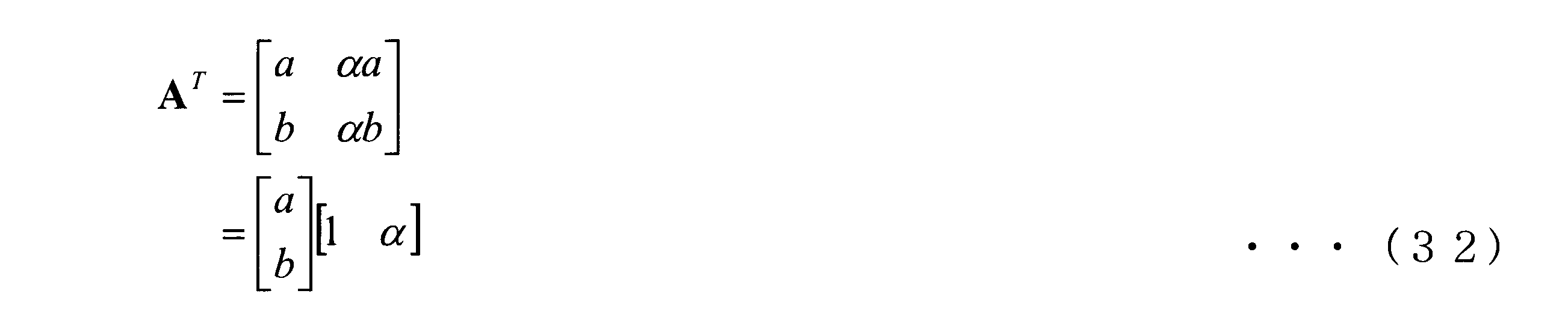
比率制約モデルC2のパラメータ(A)であるB,Q,Pは、次式(33),(34),(35)のように設定する。


第2の例、(N=3、M=3、L=1)の場合について示す。行列モデルC1のパラメータAを次式(36)のようにベクトルの積に変形する。
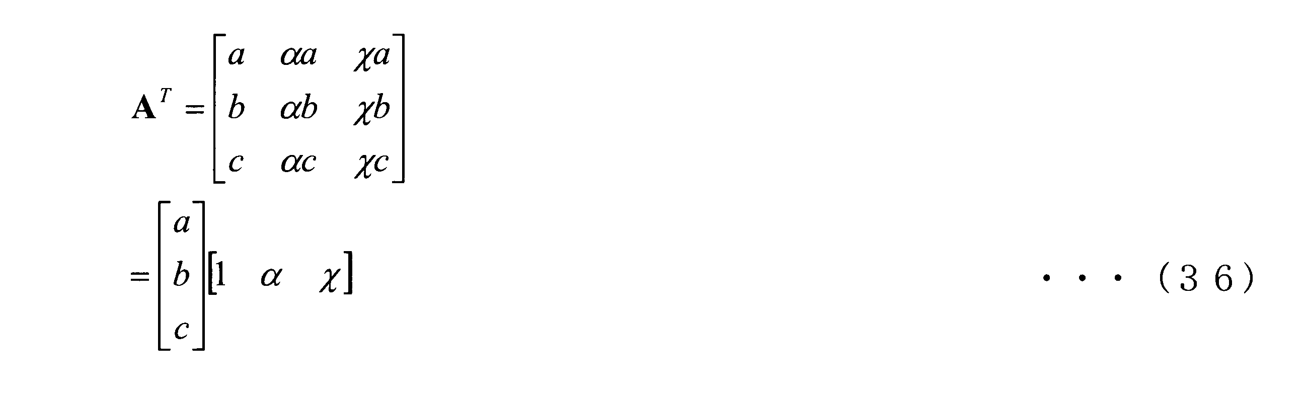
比率制約モデルC2のパラメータ(A)であるB,Q,Pは、次式(37),(38),(39)のように設定する。



第3の例、(N=3、M=3、L=2)の場合について示す。行列モデルC1のパラメータAを次式(40)のような非正方行列の積で表現する。右辺左側の行列は行列ATの線形独立な列を残して3行2列となる。右側の行列は仮に置いた。
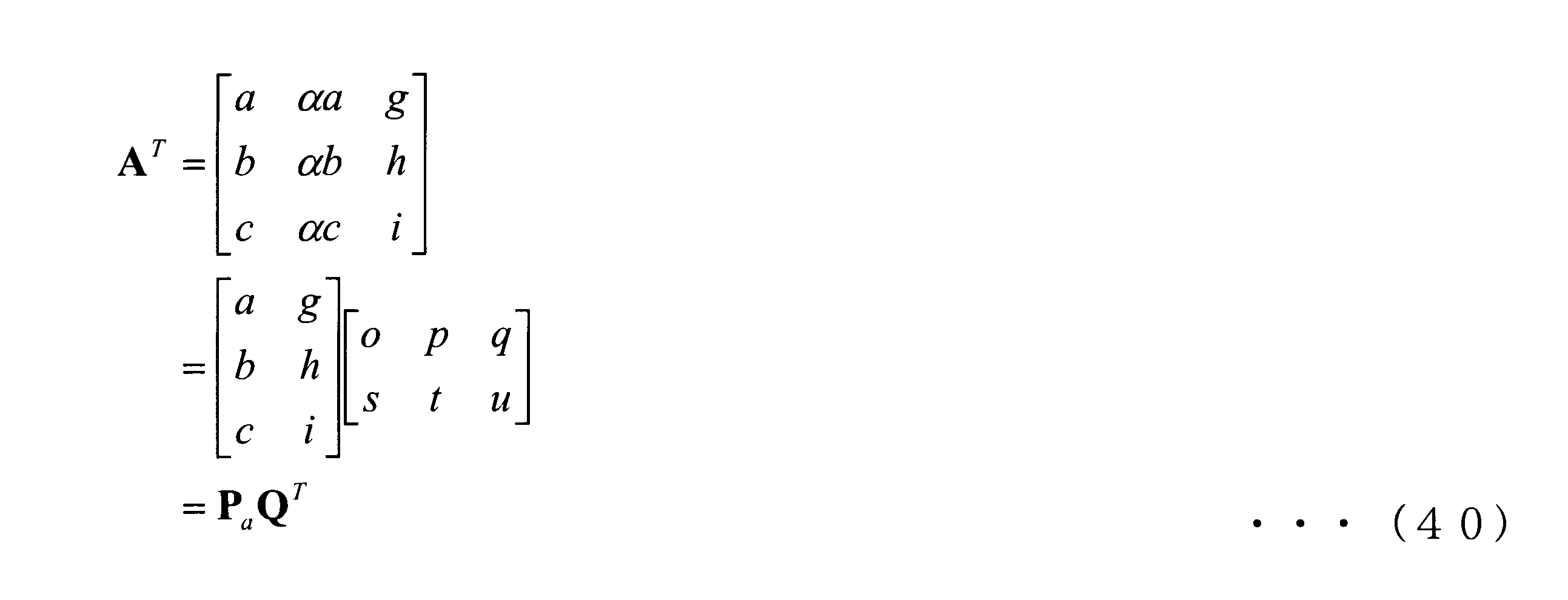
式(40)を解いてQTは次式(41)となる。

もちろんQT=(Pa
TPa)-1Pa
TATとして数値的に解いてもよい。PはP=Pa((Pa
TPa)-1)Tで求める。
なおPLS回帰分析を利用して、行列モデルC1から比率制約モデルC2のパラメータ(A)を求めることもできる。まず、行列モデルC1の入力を適宜設定して出力を算出し、多数のサンプルを作成する。そのサンプルを用いてPLS回帰分析すれば、比率制約モデルC2のパラメータであるB,Q,Pを求めることができる。新たな条件出し作業は不要である。
以上のように、実施の形態2(統合モデルC3を用いた制御)によれば、好適なエッチング制御が実現できる。
(実施の形態3)
図16~図20等を用いて、実施の形態3のエッチング装置401等について説明する。実施の形態3では、特に、行列モデルC1及び比率制約モデルC2とそれらのパラメータ(A)を定めるための、条件出しの処理方法について示す。実施の形態3における条件出し方法自体は、公知の実験計画法(DOE;Design of Experiments)に基づいて構成される。即ち各アクチュエータ値Xを何段階かの水準に設定し、各値Xの水準を組合せてエッチング処理することにより、アクチュエータ値Xの調整量(ΔX)に対する発光強度Yの変動量(ΔY)を求める方法である。簡単に言えば、ロット内の最初の数枚を処理し、以降のウェハを実験計画法による水準割付に応じたX調整量でエッチング処理し、OESで値Yをモニタする。最初の数枚の結果で値Yの経時変動モデル(Ct)のパラメータ(A)を推定し、以降のウェハ結果で値Xの調整量に応じた値Yの変動量(サンプル)を求め、これを用いて制御モデルのパラメータ(A)を算出するものである。
図16~図20等を用いて、実施の形態3のエッチング装置401等について説明する。実施の形態3では、特に、行列モデルC1及び比率制約モデルC2とそれらのパラメータ(A)を定めるための、条件出しの処理方法について示す。実施の形態3における条件出し方法自体は、公知の実験計画法(DOE;Design of Experiments)に基づいて構成される。即ち各アクチュエータ値Xを何段階かの水準に設定し、各値Xの水準を組合せてエッチング処理することにより、アクチュエータ値Xの調整量(ΔX)に対する発光強度Yの変動量(ΔY)を求める方法である。簡単に言えば、ロット内の最初の数枚を処理し、以降のウェハを実験計画法による水準割付に応じたX調整量でエッチング処理し、OESで値Yをモニタする。最初の数枚の結果で値Yの経時変動モデル(Ct)のパラメータ(A)を推定し、以降のウェハ結果で値Xの調整量に応じた値Yの変動量(サンプル)を求め、これを用いて制御モデルのパラメータ(A)を算出するものである。
実施の形態3での特長は、上記2つのモデル(C1,C2)を求めるための条件出しであること、エッチング処理における経時変動を補償してY実績値、即ちサンプル値を決めること、量産での条件出し工数低減を図るためにエッチング処理回数・ウェハ数を少なくすること、等である。
<条件出し-処理フロー>
図16のフローに従って、条件出し処理の内容を説明する。なお図16で、太枠の部分(S1201等)は、マニュアル(ユーザ)での設定処理であり、他の部分は、エッチング装置401またはその計算機411等による処理である。前述の図5の構成では、OESデータ解析システム433に条件出し機能521が実装される形態としたが、ここでは、その機能(521)はエッチング装置401に実装されて計算機411により計算処理される形態として説明する。なお、エッチング処理はエッチング装置401で実施し、設定や計算処理などはOESデータ解析システム433で実行する形態としてもよい。
図16のフローに従って、条件出し処理の内容を説明する。なお図16で、太枠の部分(S1201等)は、マニュアル(ユーザ)での設定処理であり、他の部分は、エッチング装置401またはその計算機411等による処理である。前述の図5の構成では、OESデータ解析システム433に条件出し機能521が実装される形態としたが、ここでは、その機能(521)はエッチング装置401に実装されて計算機411により計算処理される形態として説明する。なお、エッチング処理はエッチング装置401で実施し、設定や計算処理などはOESデータ解析システム433で実行する形態としてもよい。
まずS1201において、ロット内経時変動モデル(Ct1とする)を設定し、アクチュエータ代表値(Xrとする)によるエッチング処理数(ウェハ枚数)(w2とする)を設定する。ロット内経時変動モデル(Ct1)とは、ロット内の複数ウェハについてウェハ1枚ずつ連続的にエッチング処理を繰り返すことにより発生する発光強度Yの変動の表現である。これは式(14)において右辺1項目を排除した式が一例である。またアクチュエータ代表値(Xr)とは、調整量(制御量)(d7)を加えていないアクチュエータ値Xであり、即ち「制御無しのアクチュエータ(値)設定」を意味する。
図17を用いて、条件出しにおけるロット内経時変動モデル(Ct1)の必要性を説明する。グラフの横軸は条件出しでのウェハ処理順[枚]、縦軸は発光強度Yである。黒丸プロットはアクチュエータ代表値(Xr)でのエッチング処理における発光強度Yであり、白丸プロットはアクチュエータ水準組合せでのエッチング処理における発光強度Yである。発光強度Yはエッチング処理順に一定比率で上昇していくとする。この場合にはアクチュエータ水準組合せによる制御量(発光強度Yの変化量ΔY)とエッチング処理繰り返しによる発光強度Yの変化量ΔYを定量化しなければならない。そのためには、まずアクチュエータ代表値(Xr)でのエッチング処理における発光強度Y(黒丸)により経時変動の傾向であるaで示す推定線を求める。そしてアクチュエータ水準組合せでのエッチング処理における発光強度Y(白丸)と推定線(a)との差をとれば、それが水準組合せによる発光強度Yの変化量ΔY、即ち制御量である。例えば、bで示す水準組合せでの発光強度Yと推定線(a)との差が、cで示す制御量である。推定線(a)は、ロット内経時変動モデル(Ct1)を直線と設定した上で、アクチュエータ代表値(Xr)でのY実績値によりパラメータ(A)を決定して得た、制御無し発光強度のエッチング処理毎の変化を意味する線となる。このようにエッチング処理繰り返しによる発光強度Yの変動を補償してアクチュエータ値Xの調整による制御量を得るために、ロット内経時変動モデル(Ct1)とアクチュエータ代表値(Xr)によるエッチング処理が必要となる。
なお、ロット内経時変動モデル(Ct1)は、直線でなくとも、2次式などの非線形の式であってもよい。またアクチュエータ代表値(Xr)によるエッチング処理数は、例えば重回帰分析を用いてパラメータ(A)を決める場合には、当該パラメータ数以上でなければならない。アクチュエータ水準組合せのうち1つがアクチュエータ代表値(Xr)であるなら、その処理数は1つ減らしてもよい。ロット内で経時変動が無いならば、アクチュエータ代表値(Xr)によるエッチング処理は1回でよく、その発光強度Yと各水準組合せでの発光強度Yとの差が制御量である。
次にS1202で、制御に用いるアクチュエータを指定し、水準数と各水準での値Xを設定する。このアクチュエータは、調整することで発光強度Yの変化が見込まれるものを選んでおく。水準数は、値の設定が2段階ならば2水準、3段階ならば3水準などであり、各水準でのアクチュエータ値Xは、物理的に許容される範囲、もしくは所定のエッチング性能を得るために許容される範囲、などに基づき設定すればよい。例えば当該アクチュエータ値Xの設定許容範囲が-15~+15であり、3水準を設定する場合、第1水準のアクチュエータ値を-10、第2水準の値を0、第3水準の値を+10とすればよい。
次にS1203で、発光強度Yに関する情報を設定する。即ち、対象の波長、エッチングステップ、Y集計法などを設定する。これは図8のS801と同様であるが、条件出しでは、アクチュエータ値Xの調整量に対する発光強度Yの変化量ΔYを求めることが目的なので、Y目標値(d3)は特に設定不要である。
上記の設定は、計算機411に接続された画面412を介してユーザが設定を実施することを想定しているが、ファイルやDB432に設定内容を格納しておき計算機411が読み取る形態などとしてもよい。
S1204では、上記設定された情報をもとに、エッチング装置401では、水準組合せを生成して、実験対象となる水準組合せの候補を、条件出しを実施しているユーザに提示する。この提示は例えば画面412に情報を表示する形とすればよい。
図18を用いて、水準組合せについて説明する。図18は、3アクチュエータに値Xを3水準設定したときの、全アクチュエータ水準組合せを格子として表現した図である。横方向に第1のアクチュエータ値x1の水準設定、奥行き方向に第2のアクチュエータ値x2の水準設定、高さ方向に第3のアクチュエータ値x3の水準設定を表現し、水準組合せ数は、3アクチュエータの3水準乗、即ち33=27となる。このような水準組合せの設定方法(配置方法)を直交配置と呼び、水準組合せ数は、一般に、アクチュエータ数をM、水準数をqとして、Mのq乗(Mq)である。図18の格子(節点)に付された数字記号(111,211,…,122,222,…,233,333)は、水準組合せを表現しており、各々、1つ目の数字は第1のアクチュエータ値x1の水準、2つ目の数字は第2のアクチュエータ値x2、3つ目の数字は第3のアクチュエータ値x3の水準を意味する。
ここで実際に条件出しにおいてエッチング処理を行うサンプル数については注意を要する。行列モデルC1でのパラメータ(A)の算出は、3アクチュエータに対する3波長の発光強度Yの変化の関係に基づき、それぞれ波長個別にパラメータ(A)を求めることである。よって最低3サンプルでパラメータ(A)を算出可能であり、発光強度Yのばらつき(標準偏差)を算出するためには4サンプルあればよい。また比率制約モデルC2について内部モデル数(L)が1ならば、1サンプルでNIPALS(Non linear Iterative PArtial Least Squares;非線形反復部分最小2乗法)によりパラメータ(A)を算出可能である。
図18では、9サンプルを得るための9つのアクチュエータ水準組合せを実線丸囲み(311等)で示し、また4サンプルを得るための4つのアクチュエータ水準組合せを破線丸囲み(122等)で示している。各アクチュエータ値Xは全ての水準を網羅するように、即ち3水準であるならいずれのアクチュエータにも水準1,2,3が設定されるようにすることが望ましい。ユーザへの提示は、27水準組合せ、9水準組合せ、4水準組合せを提示した上で、更に任意の水準組合せを選定可能なようにする。
S1205において、ユーザにより、水準組合せを選定し、またそのウェハ数(w3とする)を設定する。水準組合せについては、例えば利用できるウェハ数、特に詳細に調べたいアクチュエータなどを鑑みて設定する。またアクチュエータ値Xの水準間の設定に応じた発光強度Yの変化よりも、同一アクチュエータ値Xにおける発光強度Yのばらつきを評価したい場合には、例えば各水準組合せでのウェハ数を2枚、3枚とすればよい。
そして上記に基づき、S1211~S1213において、前記アクチュエータ代表値(Xr)での処理数(w2)と水準組合せ数での実エッチング処理が繰り返される。S1212の実エッチング処理中には、OES410により発光強度Yをモニタする。
上記実エッチング処理の繰り返しの終了後、S1221において、OESデータより、指定された波長の発光強度Y(Y実績値)を取得する。この際、前記S1203で指定したエッチングステップ、Y集計法などに従って、発光強度Yを取得する。
S1222において、ロット内経時変動モデル(Ct1)のパラメータ(A)を求め、水準組合せのエッチング処理時における制御無し発光強度を推定する。例えば、ロット内経時変動モデル(Ct1)を次式(42)とする。

#jjは、S1211~S1213の繰り返しのウェハ1枚目からの処理数である。係数はDriftとShiftである。今2枚のウェハをアクチュエータ代表値(Xr)によりエッチング処理し、そのときの発光強度Y(サンプル)をySample
*[1],ySample
*[2]とするならば、DriftとShiftは次式(43,44)のように求まる。


これにより、式(42)に基づき、水準組合せでの制御無し発光強度を算出できる。なお、ロット内経時変動モデル(Ct1)は2次以上の高次であってもよい。またロット内経時変動モデル(Ct1)のパラメータ(A)の数よりも多くアクチュエータ代表値(Xr)によりエッチング処理し、当該パラメータ(A)を重回帰分析により推定してもよい。
S1223において、発光強度Yから制御無し発光強度を差し引き、アクチュエータ水準組合せに対する発光強度Yの変動量ΔYの実績値、即ち制御量を算出する。アクチュエータ代表値(Xr)によるエッチング処理数(w2)をNNoとすれば、変動量ΔYの実績値は、次式(45)で求まる。

ここで添え字のDOEは、条件出しにより得られた変動量ΔYの実績値であることを明示するためのものである。#combは水準組合せの番号であり、1~Ncombの数である。Ncombはアクチュエータ水準組合せ数である。
そしてS1224において、重回帰分析またはPLS回帰分析により、条件出し実績サンプル(xDOE
*[#comb],yDOE
*[#comb])を用いて、各制御モデル(C1,C2)のパラメータ(A)を推定する。行列モデルC1のパラメータであるAは次式(46),(47),(48)で求まる。


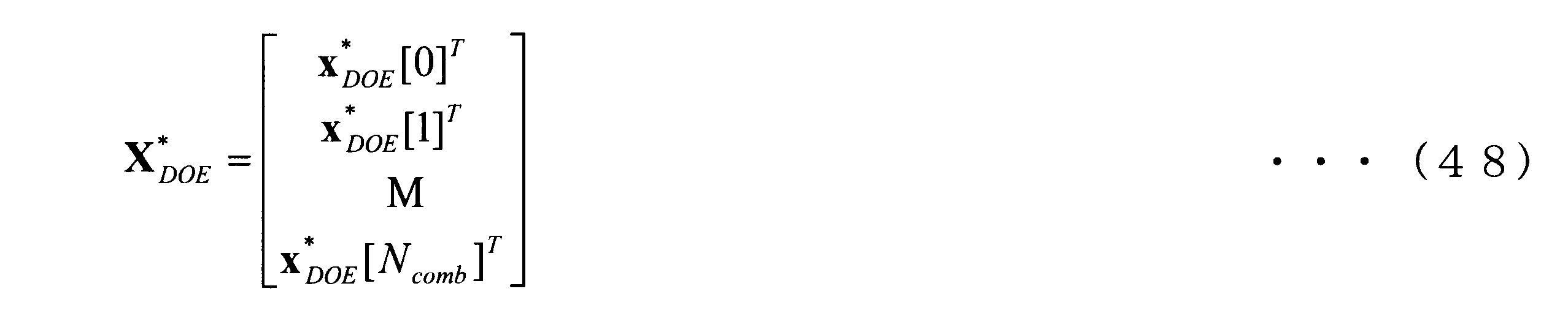
比率制約モデルC2のパラメータであるP,Q,Bは,次式(49)のようにNIPALSで求まる。

ここでNIPALS(X,Y,L)は、P,Q,Bを返す関数であり、引数は入力サンプル(X)、出力サンプル(Y)、内部モデル数(L)となる。内部モデル数であるLは、1(内部モデル最小数)から、アクチュエータ数Mと波長数Nのうち小さい数(min{M,N})、までの範囲(1≦L≦min{M,N})で設定可能である。
そしてS1225において、アクチュエータ水準組合せを用いて発光強度Yを推定し、実績値との誤差を集計する。この誤差eは、次式(50)のように、発光強度Yの実績値と推定値の差で求まる。

ここでハット“^”は推定値を意味する。行列モデルC1に基づく推定は式(51)、比率制約モデルC2に基づく推定は式(52)で算出できる。


上記の誤差集計では、平均値、標準偏差を算出する。平均が大きな値になれば、それだけモデルによる推定結果は実績値よりもずれが大きく、また標準偏差が大きければ、それだけモデルによる推定の誤差がばらつくことを意味する。いずれもゼロに近いほどモデルの推定精度は高い。
最後にS1226において、各制御モデル(C1,C2)のパラメータ(A)と誤差集計結果を提示する。これによりユーザは、いずれの制御モデルが発光強度Yを良く制御できるか等について判断できる。
上記PLS回帰分析の式(49)のNIPALSについてであるが、アクチュエータ数Mと波長数Nが等しく、更に内部モデル数Lも等しい場合、制御モデルのパラメータ(A)の推定結果は、式(46)の重回帰分析の結果と一致する。即ち、AT=P(PTP)-1BQTであり、また(AT)-1=Q(QTQ)-1B-1PTである。つまり、重回帰分析はPLS回帰分析により一般化できる。つまり、パラメータ(A)を求めるには、NIPALSのみ実装されていればよい。
また、発光強度Yを予測することによる制御モデル(C1,C2)の比較評価も可能である。全部のアクチュエータ水準組合せの条件出し実績サンプル(サンプル数Ncomb)を、今、モデルパラメータ算出用のサンプル(サンプル数Nreg)と予測用サンプル(サンプル数Npred)とに分割する。Ncomb=Nreg+Npredである。パラメータ算出用のサンプルを用いて、式(49)に基づきパラメータ(A)を算出する。算出したパラメータ(A)を「真のモデルパラメータ」とし、予測用サンプルを用いて、式(52)により発光強度Yの予測値を算出し、式(50)に基づき予測誤差を算出する。予測誤差を集計することで、各制御モデル(C1,C2)を比較評価できる。なお、この時、式(47),(48)のNcombはNregとし、また式(50),(52)の#combを予測用サンプルのインデクス、推定値を予測値と解釈する。以上が条件出し方法に従った処理内容の説明である。
<条件出し-工数低減>
半導体ウェハ生産工場(ファブ)における量産では、生産スループットが重要であり、製品ウェハそのものの生産ではない条件出しのような準備作業の工数は少ないほどよい。つまり前記アクチュエータ代表値(Xr)によるエッチング処理数(w2)、及びアクチュエータ水準組合せ数は少ないほどよい。そこで条件出しにおいて、これらの最小数の提示は有用である。
半導体ウェハ生産工場(ファブ)における量産では、生産スループットが重要であり、製品ウェハそのものの生産ではない条件出しのような準備作業の工数は少ないほどよい。つまり前記アクチュエータ代表値(Xr)によるエッチング処理数(w2)、及びアクチュエータ水準組合せ数は少ないほどよい。そこで条件出しにおいて、これらの最小数の提示は有用である。
ロット内経時変動は無いと仮定すれば、アクチュエータ代表値(Xr)によるエッチング処理数(w2)は1、もしアクチュエータ水準組合せ中にアクチュエータ代表値(Xr)が有るならば0である。ロット内経時変動が有るとすれば、その変動は線形で近似できるとして、処理数(w2)は2、もしアクチュエータ水準組合せ中にアクチュエータ代表値(Xr)が有るならば1となる。そこでアクチュエータ代表値(Xr)による処理数(w2)は、0,1,2のいずれかで決まる。
PLS回帰分析による制御モデルのパラメータの計算のためには、サンプル数は内部モデル数(L)以上必要である。内部モデル数(L)は、前述のように、1(内部モデル最小数)からmin{M,N}(内部モデル最大数)の範囲でとることができる(当該範囲内で任意)。本制御は、複数波長の発光強度Yをアクチュエータ値Xにより制御するものであるが、発光は物質に依存して多数の波長において発生するため、一般的に制御においては波長数(N)以下にアクチュエータ数(M)を設定する(N≧M)。もしくは、例えば1つの波長の発光強度Yを2つのアクチュエータで制御する場合でも、それぞれのアクチュエータ値Xにより発光強度Yがどのように変化するかを評価しなければならない。よって制御モデルCのパラメータ(A)を決めるためのサンプル数、即ちアクチュエータ水準組合せ数は、上記の内部モデル最小数(1)以上でアクチュエータ数(M)以下において定まる(1≦サンプル数≦M)。但し、ばらつき評価のために推定誤差、もしくは予測誤差を算出する必要がある。そこでアクチュエータ水準組合せ数には更にウェハ1枚分を加える。
つまり条件出しに必要となるウェハの最小枚数は、制御に用いるアクチュエータ数(M)以下の数に、ばらつき評価用の1を加え、経時変動補償のための0もしくは1もしくは2を加えた数となる。
条件出しを行った結果、アクチュエータのいずれの設定においても全ての波長における発光強度Yが変化しない場合、また全てのアクチュエータの設定においてもある波長では発光強度Yが変化しない場合、が起こり得る。図19によりこれらの場合を例示する。
図19において、(a)アクチュエータ無効、(b)波長無効、の例を示している。それぞれ2つのアクチュエータ(#1,#2)を行方向、2つの波長(A,B)を列方向にとって、アクチュエータ値Xを横軸、発光強度Yを縦軸にとったグラフを配置している。グラフ中のプロットはアクチュエータの水準毎の発光強度Yである。
図19(a)のアクチュエータ無効では、第2のアクチュエータ#2を大きい方向に調整したときには波長Aで発光強度Yはcで示すように上昇、波長Bで発光強度Yはdで示すように下降する。よって第2のアクチュエータ#2で発光強度Yを制御可能である。一方、第1のアクチュエータ#1では、aで示す波長Aでの発光強度Y、bで示す波長Bでの発光強度Yのように、明確な上昇・下降といった傾向が無い。行列モデルC1、比率制約モデルC2とも、1つのアクチュエータに対する1つの波長の発光強度Yの関係は比例関係であるため、第1のアクチュエータ#1ではこれらの波長の発光強度Yを制御できない。
図19(b)の波長無効では、波長Aにおいて第1のアクチュエータ#1を調整すれば、aで示すように発光強度Yは下降、第2のアクチュエータ#2を調整すれば、cで示すように発光強度Yは上昇するので、制御可能である。また波長Bにおいては第1のアクチュエータ#1、第2のアクチュエータ#2の調整で、それぞれbで示す発光強度Y、dで示す発光強度Yのようになり、制御不可能である。
これらのような場合には、該当のアクチュエータを制御に使用しない、もしくは該当の波長を制御対象から外す。この判断を定量的に行うためには、アクチュエータ値Xに対する発光強度Yの変化量と、条件出しでのY実績値のばらつきの大きさを比較すればよい。これについて図20により説明する。
図20には、(a)変動無し、(b)変動有りについて、アクチュエータ値Xを横軸、発光強度Yを縦軸に、Y実績値を白丸でプロットしている。aの破線は、プロットを用いた重回帰分析による発光強度Yの推定線である。(a)変動無しの場合は、アクチュエータ値Xの調整範囲における発光強度Yの変化量Δ1は、実績値と推定線aとの誤差eと比較して小さい。一方(b)変動有りの場合には、発光強度Yの変化量Δ2は誤差と比較して大きい。つまり、発光強度Yの変化量をΔ、実績値と推定線aとの誤差の標準偏差σとすれば、Δ/σにより変動有無を判定できる。Δ/σが基準値、例えば3より小さければ、発光強度Yは変動しないと判定すればよい。
全てのアクチュエータに対して、全ての波長の発光強度Yにおいて変化が見られない場合も起こり得る。このような場合、定めたアクチュエータで制御対象の波長の発光強度Yを制御できない。この場合には制御対象のアクチュエータを選定しなおす。
実施の形態3の制御の結果において、行列モデルC1のパラメータ(A)である係数行列がランク落ちをする場合、もしくは、値Xの変化量ΔXの制御量(d7)が、所定の設定許容範囲を超える場合、本制御が不可能または不適切と判定し、エラーメッセージを出力(通知、表示など)する。例えば、画面412にエラーメッセージ等の情報を表示する。また、本制御が不可能または不適切と判定した場合、エッチング装置401での実エッチング処理については自動的に停止させるようにしてもよいし、続行させるようにしてもよい。
以上のように、実施の形態3(制御モデルCとそのパラメータ(A)を決定するための条件出し方法)によれば、好適なエッチング制御が実現できる。
(実施の形態4)
図21等を用いて、実施の形態4のエッチング装置401等について説明する。実施の形態4では、複数アクチュエータ値Xにより複数波長の発光強度YをRun-to-Run制御したときの制御性能、即ちY目標値に対する制御結果発光強度Y(Y実績値)の誤差を、実エッチング処理すること無く評価するための制御シミュレーションについて説明する。
図21等を用いて、実施の形態4のエッチング装置401等について説明する。実施の形態4では、複数アクチュエータ値Xにより複数波長の発光強度YをRun-to-Run制御したときの制御性能、即ちY目標値に対する制御結果発光強度Y(Y実績値)の誤差を、実エッチング処理すること無く評価するための制御シミュレーションについて説明する。
実施の形態4の基本的な処理内容は図8のフローの通りであるが、制御シミュレーションでは、実際にエッチング装置401でエッチング処理すること無くY実績値(その相当値)を算出する必要がある。そこでY実績値を算出するための制御モデルCを「真の制御モデル」(Cb)として定義し、アクチュエータ値Xを算出する制御モデルCについては、制御用に設定した制御モデル(Ca)とした。また、制御無し発光強度の経時変動の補償についても、その制御用の制御モデル(Ca)を用いる。この制御用の制御モデル(Ca)は、実制御(実際のRun-to-Run制御)で設定・使用する制御モデルCに相当する。「真の制御モデル」(Cb)と制御用の制御モデル(Ca)との違いにより、Y実績値は目標値からずれることとなる。よって各制御モデルCの制御性能を評価できる。なお制御モデルCのパラメータ(A)の違いによる制御性能の評価も同様である。
なお制御無し発光強度の経時変動についても「真の経時変動」があり、「真の制御無し発光強度」の経時変動データを用いてY実績値を算出しなければならない。但し制御における制御無し発光強度の経時変動の補償には、制御用の制御モデル(Ca)を用い、また制御用に設定した経時変動モデル、フィルタ等を用いる。
<制御シミュレーション-処理フロー>
図21のフローに従って、制御シミュレータ434による制御シミュレーションの処理内容を説明する。本処理内容は、全て制御シミュレータ434(その計算機システム)により実行される。
図21のフローに従って、制御シミュレータ434による制御シミュレーションの処理内容を説明する。本処理内容は、全て制御シミュレータ434(その計算機システム)により実行される。
S1701において、「真の制御モデル」(Cb)と制御モデルCのパラメータ(A)を読み込む。制御モデルCの定義自体に、入力である波長数(N)、アクチュエータ数(M)が含まれる。しかしシミュレーションでは、波長[nm]の情報やアクチュエータ種類といった情報は不要である。制御モデルCが行列モデルC1の場合にはそのパラメータであるAtrue、比率制約モデルC2の場合にはパラメータであるPtrue,Qtrue,Btrueを読み込み、統合モデルC3の場合にはそのパラメータであるAtrue,Ptrue,Qtrue,Btrueの他に分配係数DMAT
true,DRC
true(もしくはベクトルDMAT
true,DRC
true)を読み込む。C2,C3の場合には内部モデル数(L)の情報も読み込む。
S1702において、制御用の制御モデル(Ca)とそのパラメータ(A)を読み込む。パラメータ(A)は、A,P,Q,B,DMAT,DRC(もしくはベクトルDMAT,DRC)のいずれか、もしくは全てである。
S1703において、複数波長の発光強度Yの目標値yTGTと、制御無し発光強度の初期値yNo[0][0]を読み込む。
S1704において、ロット数、ロット内ウェハ数のデータを読み込む。
S1705において、「真の制御無し発光強度」の経時変動データであるytrue[#ii][#jj]を読み込む。#iiはロット順序を表すインデクス、#jjはロット内ウェハ順序(エッチング処理順)を表すインデクスである。ロット数、ロット内ウェハ数は、S1704で読み込んだデータにおける数と一致していなければならない。
S1706において、制御無し発光強度の経時変動を補償するための設定情報を読み込む。これは、ノイズを除去し経時変動を平滑化するフィルタパラメータや経時変動モデル(Ct)とそのパラメータ(A)の初期値が対象である。フィルタが例えばEWMA(Exponentially-Weighted Moving Average)フィルタであるなら、パラメータlを読み込む。経時変動モデル(Ct)が式(14)で定義されるなら、そのパラメータ(A)であるDriftlot,Driftwaferの初期値を読み込む。
以降、S1711~S1717の処理が、ロット毎、及びロット内のウェハ毎の繰り返し計算となる。今、ロット繰り返し#ii回目、ロット内ウェハ(エッチング処理)繰り返し#jj回目の処理とする。繰り返し開始からの全繰り返しは#kk回目とする。
S1713において、アクチュエータ値Xを算出する(図8のS807と同様の計算)。まず制御無し発光強度であるyNo[#ii][#jj]が必要であるが、これは前回の制御無し発光強度の算出の結果を利用するか、例えば式(14)のような経時変動モデル(Ct)に基づき算出する。そして式(15)により制御量を求めて、行列モデルC1ならば式(8)、比率制約モデルC2ならば式(13)、統合モデルC3ならば式(25)~(29)により、アクチュエータ値であるx[#ii][#jj]を算出する。なおC3の場合、xMAT[#ii][#jj],xRC[#ii][#jj]の算出結果も記憶しておく。設定制御量についても、行列モデルC1ならば式(7)、比率制約モデルC2ならば式(12)、統合モデルC3ならば式(21)もしくは式(23)により求めておく。
S1714において、Y実績値を算出する。Y実績値は、「真の制御無し発光強度」の経時変動データであるytrue[#ii][#jj]と「真の制御モデル」(Cb)による制御量であるymodel
trueとの和である。即ち次式(53)である。

ここで、制御量は、行列モデルC1なら式(54)、比率制約モデルC2なら式(55)、統合モデルC3なら式(56)で求まる。



S1715において、制御無し発光強度を算出し、経時変動を補償する。式(16)で制御無し発光強度の実績値を算出し、例えばEWMAフィルタを用いて経時変動を補償する場合には式(17),(18)を用いて、制御無し発光強度を算出する。また経時変動モデル(Ct)を用いてアクチュエータ値Xの算出時に制御無し発光強度を算出する場合には、式(19),(20)のように経時変動モデル(Ct)のパラメータ(A)を更新すればよい。
そして全ての繰り返しの終了後、S1721において、アクチュエータ値Xの算出結果、Y実績値と目標値からの誤差を集計する。アクチュエータ値Xの算出結果であるx[#ii][#jj]、Y実績値であるy*[#ii][#jj]、Y実績値と目標値との誤差であるe[#ii][#jj]=y*[#ii][#jj]-yTGTの、平均、標準偏差、最大、最小といった統計量を集計計算により求めればよい。
上記制御用の制御モデル(Cb)とそのパラメータ(A)を変更して制御シミュレーションを行うことで、設定に対する制御性能を比較評価可能となる。
図21のフローにより、「真の制御無し発光強度」データを直接に読み込んでのシミュレーションを説明した。「真の制御無し発光強度」データとは、実際にアクチュエータ値Xを調整しないでエッチング処理を繰り返すことにより得られるデータである。実制御(実エッチング処理)を実施しているエッチング装置401ではこのデータを直接に取得することはできない。つまり式(53)の左辺のy*[#ii][#jj]を取得することになる。そこで実エッチング処理したときのアクチュエータ値Xと制御モデルC及びそのパラメータ(A)を取得し、当該制御モデルCに応じて、式(54),(55),(56)に応じて制御量を求める。これにより式(53)に基づき「真の制御無し発光強度」の経時変動データであるytrue[#ii][#jj]を作成できる。
また「真の制御無し発光強度」の経時変動データを、経時変動モデル(Ct)により生成して制御シミュレーションすることも可能である。この場合、図21のS1721では、「真の経時変動モデル」パラメータを読み込む。例えば式(14)の経時変動モデル(Ct)とするならば、Driftlot
true,Driftwafer
trueを読み込む。またデータにばらつきを与えるために、ばらつきの大きさのパラメータであるσtrueも読み込む。そしてS1714のY実績値の算出の際に、次式(57)により「真の制御無し発光強度」データであるytrue[#ii][#jj]を算出する。

ここでN(m,σ2)は平均m、分散σ2の正規分布に従う乱数である。
以上の制御シミュレーションにおいては、「真の制御モデル」(Cb)に基づきY実績値を算出する形態として説明したが、他にも例えば物理的な根拠に基づくシミュレータ(プロセスシミュレータ)を利用して、算出したアクチュエータ値Xによる制御量を求めてからY実績値を求めても、制御シミュレーションは可能である。
以上のように、実施の形態4(Run-to-Run制御シミュレーション)によれば、好適なエッチング制御が実現できる。
(効果等)
以上説明したように、実施の形態によれば、(1)制御モデルCを用いた好適なRun-to-Run制御の実現、(2)X値の異常を防止(許容範囲内に限定)しながらY目標値へ近付ける制御の実現、(3)好適なパラメータ(A)を決定する条件出しの実現、(4)Run-to-Run制御シミュレーションの実現、等の効果がある。詳しくは以下が挙げられる。
以上説明したように、実施の形態によれば、(1)制御モデルCを用いた好適なRun-to-Run制御の実現、(2)X値の異常を防止(許容範囲内に限定)しながらY目標値へ近付ける制御の実現、(3)好適なパラメータ(A)を決定する条件出しの実現、(4)Run-to-Run制御シミュレーションの実現、等の効果がある。詳しくは以下が挙げられる。
実施の形態1,2等において、エッチング装置401の複数アクチュエータ値Xの調整量を設定許容範囲内で算出できるので、エッチング処理不良などを防止できる。またその範囲に応じて複数波長の発光強度Yを目標値に近付けることができる。
複数波長の発光強度Yの制御は、チャンバ402内のエッチング現象に係る複数種類の物質の量の制御に相当する。つまり複数の物質の化学反応によってエッチングされて出来る形状や異なる組成の膜のエッチング量を制御できる。深さ方向と横方向のエッチングレートに影響するガスやバイアス電圧を、上記アクチュエータ値X(即ちエッチング処理条件等)として制御して、目標とする断面形状を得ることができる。多層構造の膜のエッチングにおいて、各層のエッチングの反応に影響するアクチュエータでエッチングレートを制御することで、特定層のエッチング量の過不足を防止できる。エッチングでの反応生成物の増加に対して、その反応生成物を別の物質へと反応させることにより、特定の異物の生成を抑制することができる。有機膜などの複雑な組成を持つ膜をエッチングする際に、多種多様な物質の発生がエッチングレートの経時変動に影響する場合、各物質の発生量を一定にしてエッチングレートを安定化することができる。
またOES410はエッチング処理中の発光をモニタするものであるため、別途検査装置でウェハを検査すること無くエッチングの性能を推定できる。従って、連続的にエッチング処理が繰り返されるロット内のウェハ毎にアクチュエータ値Xを調整でき、またロット毎にも検査結果を待つことなく着工を繰り返すことができる。よってエッチング装置スループットを落とすことなく、エッチング処理を安定化し、例えばCD寸法を高精度化できる。
また、実施の形態3の条件出しにおいては、比率制約モデルC2のパラメータ(A)を決定する際に、PLS回帰分析を利用する。本分析方法では、例えば1組のサンプルであってもパラメータを算出可能であり、重回帰分析のようなパラメータ数以上のサンプル数は必要無い。つまり少ないサンプル数でパラメータを決定でき、実験工数、及び実験のためのウェハ数などを削減できる。
また、実施の形態4の複数アクチュエータによる複数波長の発光強度Yの制御シミュレーションを活用すれば、制御モデルCに含まれる多数のパラメータを変更した際の制御性能の変化を容易に机上で評価可能となる。よって制御結果を良好とするパラメータを効率的に見出して適用することができる。また発光強度Yの経時変動の大きさやエッチング処理毎のばらつきの大きさが変わった場合にも、同様に机上で評価できる。
本発明は前記実施の形態に限定されるものではなく、その要旨を逸脱しない範囲で種々変更可能である。例えば、前記実施の形態の説明では、OES410でモニタしたプラズマの発光強度Yを制御対象としたが、これに限らず例えば、処理中のウェハの光学的膜厚モニタや、ウェハ近傍の電磁界モニタ、更には赤外線などを用いて検出したスペクトル等、モニタ値が多変量となる場合には、そのモニタ値を制御対象として適用可能である。
本発明は、半導体製造管理システムなどに利用可能である。
401…エッチング装置、402…チャンバ、403,406…電極、404…プラズマ、405…ウェハ、407…排気系、408…ガス供給系、409…装置コントローラ、410…OES(発光分光器)、411…計算機、412…画面、413…流量調整装置、414…圧力調整装置、415…電力調整装置、416…温度調整装置、421…窓、422…光、431…ネットワーク、432…DB、433…OESデータ解析システム、434…制御シミュレータ、501…Run-to-Run制御機能、501B…Run-to-Run制御機能、502…ロット・ウェハ毎エッチング処理来歴取得機能、503…制御モデル設定機能、504…発光波長・発光強度目標値設定機能、505…制御用アクチュエータ設定機能、506…複数発光波長強度制御量算出機能、507…アクチュエータ値算出機能、508…アクチュエータ値指令機能、509…OESデータ取得機能、510…複数波長発光強度取得機能、511…発光強度経時変動量取得機能、521…条件出し機能、522…アクチュエータ水準組合せ設定機能、523…複数波長発光強度取得機能、524…制御モデル毎モデルパラメータ算出機能、525…発光強度推定誤差算出・評価機能、526…発光強度予測用アクチュエータ値算出機能、527…真の制御モデル設定機能、528…発光強度算出・評価機能、529…複数波長発光強度目標値取得機能、530…複数波長発光強度制御量算出機能、531…アクチュエータ値算出・評価機能、541…真の制御モデル設定機能、542…複数波長発光強度算出機能、543…制御無し発光変動取得機能、544…制御有り発光変動取得機能、545…制御無し発光変動算出機能。
Claims (21)
- チャンバ内部のプラズマ発光を観察するための発光分光器と、前記プラズマ発光を調整するための複数のアクチュエータとを備え、ウェハのエッチング処理を行うエッチング装置であって、
本エッチング装置に備える制御機能において、
前記複数のアクチュエータの値をXとし、前記発光分光器によりモニタされる前記プラズマ発光の複数の波長の発光強度の値をYとしたとき、前記エッチング処理で適用する複数のアクチュエータの値Xの設定値(d1)と、前記エッチング処理で前記発光分光器によりモニタされる前記複数の波長の発光強度の値Yの実績値(d2)との関係について、値Xの変化量ΔXと、各値Xに対する値Yの変化量ΔYとの関係が、変化量ΔXを入力とし変化量ΔYを出力とした代数的な数式に基づく制御モデルとして定義され、
前記制御モデル及びそれに含まれるパラメータの値が予め設定され、
前記複数の波長の発光強度の値Yの目標値(d3)が予め設定され、
前記エッチング処理の制御の処理として、
(S1)前記ウェハのエッチング処理の開始の前に、前記値Yの目標値(d3)と、複数の制御無し発光強度の値Y(d4)との差分値(d5)を、前記値Yに関する目標制御量(d6)とし、前記制御モデルに基づき、当該値Yの目標制御量(d6)から、前記複数のアクチュエータの値Xに関する制御量(d7)を算出し、当該値Xの制御量(d7)を、前記複数のアクチュエータに対して前記設定値(d1)として適用する、第1の処理ステップと、
(S2)次に前記ウェハのエッチング処理を開始し、前記発光分光器により所定の時間間隔で前記プラズマ発光のスペクトルの前記複数の波長の発光強度の値Yをモニタしながら、当該エッチング処理を終了する、第2の処理ステップと、
(S3)次に前記モニタのデータによる、または当該データの中から所定の時間単位で取得される、前記複数の波長の発光強度の値Yの実績値(d2)を用いて、当該値Yの実績値(d2)と前記目標値(d3)との誤差(d8)と、前記第1の処理ステップで算出した前記値Xの制御量(d7)とに基づき、次のウェハのエッチング処理で用いるための、前記複数の制御無し発光強度の値(d4)を計算する第3の処理ステップと、を有し、
前記第1~第3の処理ステップを各ウェハのエッチング処理で繰り返し実行する制御により、前記複数のアクチュエータ値Xを調整し、前記複数の波長の発光強度値Yを制御する、ことを特徴とするエッチング装置。 - 請求項1記載のエッチング装置において、
前記制御モデルにおける各値の関係は、前記値Xの変化量ΔXを入力とし前記値Yの変化量ΔYを出力とした行列方程式もしくは連立方程式による第1の制御モデルとして定義される、ことを特徴とするエッチング装置。 - 請求項1記載のエッチング装置において、
前記制御モデルにおける各値の関係は、前記値Xの変化量ΔXにおける当該アクチュエータ間の関係に第1の比率が定義され、前記値Yの変化量ΔYにおける当該波長間の関係に第2の比率が定義され、前記第1の比率と前記第2の比率との関係が所定の比例関係で定義された、第2の制御モデルとして定義される、ことを特徴とするエッチング装置。 - 請求項1記載のエッチング装置において、
前記制御モデルにおける各値の関係は、前記値Xの変化量ΔXにおける当該アクチュエータ間の関係が複数の第1の比率で定義され、前記値Yの変化量ΔYにおける当該波長間の関係が複数の第2の比率で定義され、前記複数の第1の比率の各々と前記複数の第2の比率の各々との所定の対応する比率同士の関係が所定の比例関係で定義された、第2の制御モデルとして定義される、ことを特徴とするエッチング装置。 - 請求項1記載のエッチング装置において、
前記制御モデルにおける各値の関係は、
第1に、前記値Xの変化量ΔXを入力とし前記値Yの変化量ΔYを出力とした行列方程式もしくは連立方程式による第1の部分的な制御モデルとして定義され、
第2に、前記値Xの変化量ΔXにおける当該アクチュエータ間の関係に第1の比率が定義され、前記値Yの変化量ΔYにおける当該波長間の関係に第2の比率が定義され、前記第1の比率と前記第2の比率との関係が所定の比例関係で定義された、第2の部分的な制御モデルとして定義され、
更に、前記第1の部分的な制御モデルと前記第2の部分的な制御モデルとを統合した第3の制御モデルが定義される、ことを特徴とするエッチング装置。 - 請求項5記載のエッチング装置において、
前記制御機能は、前記第1の処理ステップでの前記制御モデルに基づく前記値Xに関する制御量(d7)の算出において、
前記値Yの目標制御量(d6)は、2つの制御量に分配され、そのうち第1の制御量を第1の目標値として、前記第1の部分的な制御モデルに基づき、一方の第1のアクチュエータの値Xの変化量ΔXに関する第1の制御量を算出し、そのうち第2の制御量を第2の目標値として、前記第2の部分的な制御モデルに基づき、他方の第2のアクチュエータの値Xの変化量ΔXに関する第2の制御量を算出し、上記算出した第1と第2の制御量を加算することにより、前記値Xに関する制御量(d7)を得る、ことを特徴とするエッチング装置。 - 請求項2記載のエッチング装置において、
前記制御機能は、前記第1の制御モデルの前記パラメータである係数行列がランク落ちをする場合、もしくは前記値Xの制御量(d7)が前記設定値(d1)に関する所定の設定許容範囲を超える場合、本制御が不可能または不適切と判定し、エラーメッセージを出力する、ことを特徴とするエッチング装置。 - 請求項2記載のエッチング装置において、
前記制御機能は、
前記第1の制御モデルの前記パラメータである係数行列がランク落ちをする場合、もしくは前記値Xの制御量(d7)が前記設定値(d1)に関する所定の設定許容範囲を超える場合、前記第1の制御モデルの前記パラメータである係数行列を、第2の制御モデルのパラメータに変換して、当該第2の制御モデルを新たに前記制御に適用し、
前記第2の制御モデルは、前記値Xの変化量ΔXにおける当該アクチュエータ間の関係に第1の比率が定義され、前記値Yの変化量ΔYにおける当該波長間の関係に第2の比率が定義され、前記第1の比率と前記第2の比率との関係が所定の比例関係で定義される、ことを特徴とするエッチング装置。 - 請求項1記載のエッチング装置において、
前記エッチング処理及びその制御は、ロット単位の複数ロット間、及びロット内のウェハ単位の複数ウェハ間を対象とし、
前記制御機能は、前記第3の処理ステップでの前記制御無し発光強度の値Y(d4)の計算において、
前記ウェハのエッチング処理のウェハ枚数(w1)に関する前記制御無し発光強度の値Y(d4)が、前記値Yに関する経時変動モデルとして定義され、
前記値Yの実績値(d2)のデータと前記値Yの目標値(d3)との誤差(d8)、及び前記第1の処理ステップで算出した前記値Xの変化量ΔXに関する制御量(d7)を用いて、前記値Yの経時変動モデルのパラメータを算出し、上記算出した経時変動モデルのパラメータにより、前記制御無し発光強度の値Y(d4)を計算する、ことを特徴とするエッチング装置。 - 請求項1記載のエッチング装置において、
前記制御モデルに含まれるパラメータの値の設定のための条件出しの処理を行う条件出し機能を有し、
前記条件出し機能による条件出しの処理において、
前記ウェハのエッチング処理のウェハ枚数(w1)に関する、前記制御無し発光強度の値Y(d4)が、当該ウェハ枚数(w1)に関する前記値Yの実績値(d2)の変動を表現する制御モデルである経時変動モデルとして定義され、
前記複数のアクチュエータの値Xを代表値に設定して連続的にエッチング処理するウェハ枚数(w2)が設定され、
前記複数のアクチュエータについて実験計画法を適用して水準設定した各アクチュエータの値Xの設定値とその水準設定数に相当するウェハ枚数(w3)とが設定され、
第1に、前記複数のアクチュエータの値Xを前記代表値に設定して前記発光分光器により前記複数の波長の発光強度の値Yをモニタする前記エッチング処理を、前記設定したウェハ枚数(w2)分連続的に行い、
第2に、引き続き、前記水準設定した各値Xの設定値で前記発光分光器により前記複数の波長の発光強度の値Yをモニタする前記エッチング処理を、前記水準設定数に相当するウェハ枚数(w3)分連続的に行い、
上記第1の連続的なエッチング処理における前記複数の波長の発光強度の値Yを1つ以上取得し、各波長別に、前記経時変動モデルのパラメータを算出し、
上記第2の連続的なエッチング処理における前記複数の波長の発光強度の値Yを1つ以上取得し、また前記経時変動モデルに基づき各エッチング処理でのウェハ枚数(w1)に応じた各波長の発光強度の値Yを算出し、上記取得した1つ以上の値Yから上記算出した各波長の値Yを差し引くことにより、各波長の水準設定に対する発光強度の値Yの変化量ΔYを求め、
前記値Xの設定値の水準間の1つ以上の変化量ΔXと、前記値Yの1つ以上の変化量ΔYとの組合せサンプルより、前記制御モデルのパラメータを算出する、ことを特徴とするエッチング装置。 - 請求項10記載のエッチング装置において、
前記条件出し機能は、重回帰分析により前記制御モデルのパラメータを算出する、ことを特徴とするエッチング装置。 - 請求項10記載のエッチング装置において、
前記条件出し機能は、PLS回帰分析により前記制御モデルのパラメータを算出する、ことを特徴とするエッチング装置。 - 請求項10記載のエッチング装置において、
前記複数のアクチュエータの値Xの変化量ΔXの関係を表す第1の比率の数と、前記複数の波長の発光強度の値Yの変化量の関係を表す第2の比率の数と、前記第1の比率と第2の比率との比例関係の数とが同じ数(p)であり、
前記条件出し機能は、
前記複数のアクチュエータの数(M)と前記複数の波長の数(N)とにおける小さい方の数をmin{M,N}としたとき、上記の数(p)を、1からmin{M,N}まで、それぞれ設定し、前記組合せサンプルを用いて、PLS回帰分析により、前記制御モデルのパラメータを算出し、前記組合せサンプルの前記値Xの設定値の変化量ΔXを用いて、前記値Yの変化量ΔYを、上記設定した数(p)に対応する数の制御モデルにより推定して、前記値Yの変化量ΔYとの誤差を求め、前記誤差が最も小さくなる上記の数(p)を選定することにより、前記設定のための前記制御モデルを決定する、ことを特徴とするエッチング装置。 - 請求項10記載のエッチング装置において、
前記複数のアクチュエータ値Xの変化量の関係を表す第1の比率の数と、前記複数の波長の発光強度値Yの変化量の関係を表す第2の比率の数と、前記第1の比率と第2の比率との比例関係の数とが同じ数(p)であり、
前記条件出し機能は、
前記複数のアクチュエータの数(M)と前記複数の波長の数(N)とのうちの小さい方の数をmin{M,N}としたとき、上記の数(p)を、1からmin{M,N}まで、それぞれ設定し、前記組合せサンプルのうちの一部の第1のサンプルを用いて、PLS回帰分析により、前記制御モデルのパラメータを算出し、前記組合せサンプルのうちの残りの第2のサンプルの前記複数のアクチュエータの値Xの設定値の変化量ΔXを用いて、前記複数の波長の発光強度の値Yの変化量ΔYを、上記設定した数(p)に対応する数の制御モデルにより予測して、前記第2のサンプルの前記値Yの変化量ΔYとの誤差を求め、前記誤差が最も小さくなる上記の数(p)を選定することにより、前記設定のための前記制御モデルを決定する、ことを特徴とするエッチング装置。 - 請求項10記載のエッチング装置において、
前記エッチング処理するウェハの必要枚数について、
前記代表値に設定して連続的にエッチング処理するウェハ枚数(w2)は、0または1または2とし、
前記水準設定した各アクチュエータの値Xの設定値の水準組合せ数でエッチング処理するウェハ枚数(w3)は、1以上で前記アクチュエータの数(M)以下の数に、ばらつきを評価するための1枚を加えた数とする、ことを特徴とするエッチング装置。 - 請求項10記載のエッチング装置において、
前記条件出し機能は、
前記値Xの設定値の水準間の1つ以上の変化量ΔXと、前記値Yの1つ以上の変化量ΔYとの組合せサンプルにおいて、いずれのアクチュエータにおいても当該水準間で値Yの変化量ΔYに変化が見られない場合、または、当該水準間で上昇もしくは下降の傾向よりも値Yのばらつきが大きい場合、当該波長を前記制御の対象から除外する、ことを特徴とするエッチング装置。 - 請求項10記載のエッチング装置において、
前記値Xの設定値の水準間の1つ以上の変化量ΔXと、前記値Yの1つ以上の変化量ΔYとの組合せサンプルにおいて、いずれの波長においても当該水準間で値Yの変化量ΔYに変化が見られない場合、または、当該水準間で上昇もしくは下降の傾向よりも値Yのばらつきが大きい場合、当該アクチュエータを前記制御の対象から除外する、ことを特徴とするエッチング装置。 - エッチング装置でのウェハのエッチング処理の制御に関するシミュレーションの処理を計算機上で行う制御シミュレータであって、
前記エッチング装置の複数のアクチュエータの値をXとし、前記エッチング装置の発光分光器によりモニタされるプラズマ発光の複数の波長の発光強度の値をYとしたとき、値Xの変化量ΔXと、各値Xに対する値Yの変化量ΔYとの関係が、変化量ΔXを入力とし変化量を出力とした代数的な数式に基づく制御モデルとして定義され、
前記制御モデル及びそれに含まれるパラメータの値は、前記制御で適用される第1のモデルと、真の第2のモデルとが事前に設定され、
前記複数の波長の発光強度の値Yの目標値が事前に設定され、
前記制御をしない場合の前記ウェハ毎の前記複数の波長の発光強度の値Yの経時変動データが、事前に設定され、
1枚目のウェハの処理のために、前記制御をしない場合の前記値Yの推定値の初期値を、前記ウェハ毎の値Yの経時変動データの1回目の値とし、
所定のウェハ処理枚数における1枚目のウェハから最後のウェハまで順に行う前記シミュレーションの処理において、
前記ウェハのエッチング処理の開始の前に、前記値Yの目標値と、前記制御をしない場合の前記値Yの推定値との差を、目標制御量として、前記制御モデルのパラメータを設定値として、前記第1のモデルに基づき前記値Xの制御量を算出して、前記複数のアクチュエータの値Xの設定値とする第1の処理ステップと、
前記ウェハのエッチング処理として、前記ウェハ処理枚数に応じた前記値Yの経時変動データに、前記真の第2のモデルに基づき前記値Xより算出した前記値Yの1つ以上の変化量ΔYを加え、前記発光分光器による前記値Yのモニタ値とする第2の処理ステップと、
前記値Yの1つ以上のモニタ値と前記値Yの目標値との誤差と、前記第1の処理ステップで算出した値Xの制御量とを用いて、前記制御をしない場合の前記値Yの推定値を計算する第3の処理ステップと、を有し、
前記第1~第3の処理ステップの繰り返しで求めた全ウェハの処理の前記値Yのモニタ値を集計して、前記値Yの目標値との誤差を評価する、ことを特徴とする制御シミュレータ。 - 請求項18記載の制御シミュレータにおいて、
前記制御をしない場合の前記ウェハ毎の前記複数の波長の発光強度の値Yの経時変動データとは、
ウェハ毎のアクチュエータ値を調整して発光強度を制御したエッチング処理において、発光分光器でモニタした発光強度と、アクチュエータ値を調整した際に目標とした制御量とにより求めた発光強度である、ことを特徴とする制御シミュレータ。 - 請求項18記載の制御シミュレータにおいて、
前記制御をしない場合の前記ウェハ毎の前記複数の波長の発光強度の値Yの経時変動データについては、
前記ウェハ処理枚数に関する、前記制御をしない場合の前記値Yの経時変動を表現する経時変動モデルが定義され、
前記経時変動モデルのパラメータが設定され、
前記ウェハ処理枚数が設定され、
1枚目のウェハのエッチング処理から順に、前記経時変動モデルに基づき、前記値Yが算出され、または、前記経時変動モデルのパラメータを乱数と演算して更新して当該経時変動モデルに基づき前記値Yが算出される、ことを特徴とする制御シミュレータ。 - チャンバ内部のプラズマ発光を観察するための発光分光器と、前記プラズマ発光を調整するための複数のアクチュエータとを備え、ウェハのエッチング処理を行うエッチング装置、によるエッチング工程を含む、半導体装置製造方法であって、
前記エッチング工程及びその制御は、ロット単位の複数ロット間、及びロット内のウェハ単位の複数ウェハ間を対象とし、
前記複数ロット及びその複数ウェハが前記エッチング装置に対して連続的に着工され、
前記ウェハ着工毎の前記エッチング工程において、
前記複数のアクチュエータの値をXとし、前記発光分光器によりモニタされる前記プラズマ発光の複数の波長の発光強度の値をYとしたとき、前記エッチング処理で適用する複数のアクチュエータの値Xの設定値(d1)と、前記エッチング処理で前記発光分光器によりモニタされる前記複数の波長の発光強度の値Yの実績値(d2)との関係について、値Xの変化量ΔXと、各値Xに対する値Yの変化量ΔYとの関係が、変化量ΔXを入力とし変化量ΔYを出力とした代数的な数式に基づく制御モデルとして定義され、
前記制御モデル及びそれに含まれるパラメータの値が予め設定され、
前記複数の波長の発光強度の値Yの目標値(d3)が予め設定され、
前記エッチング処理の制御の処理として、
(S1)前記ウェハのエッチング処理の開始の前に、前記値Yの目標値(d3)と、複数の制御無し発光強度の値Y(d4)との差分値(d5)を、前記値Yに関する目標制御量(d6)とし、前記制御モデルに基づき、当該値Yの目標制御量(d6)から、前記複数のアクチュエータの値Xに関する制御量(d7)を算出し、当該値Xの制御量(d7)を、前記複数のアクチュエータに対して前記設定値(d1)として適用する、第1の処理工程と、
(S2)次に前記ウェハのエッチング処理を開始し、前記発光分光器により所定の時間間隔で前記プラズマ発光のスペクトルの前記複数の波長の発光強度の値Yをモニタしながら、当該エッチング処理を終了する、第2の処理工程と、
(S3)次に前記モニタのデータによる、または当該データの中から所定の時間単位で取得される、前記複数の波長の発光強度の値Yの実績値(d2)を用いて、当該値Yの実績値(d2)と前記目標値(d3)との誤差(d8)と、前記第1の処理工程で算出した前記値Xの制御量(d7)とに基づき、次のウェハのエッチング処理で用いるための、前記複数の制御無し発光強度の値(d4)を計算する第3の処理工程と、を有し、
前記第1~第3の処理工程を各ウェハのエッチング処理で繰り返し実行する制御により、前記複数のアクチュエータ値Xを調整し、前記複数の波長の発光強度値Yを制御する、ことを特徴とする半導体装置製造方法。
Priority Applications (1)
| Application Number | Priority Date | Filing Date | Title |
|---|---|---|---|
| US13/514,708 US8924001B2 (en) | 2010-02-26 | 2010-12-03 | Etching apparatus, control simulator, and semiconductor device manufacturing method |
Applications Claiming Priority (2)
| Application Number | Priority Date | Filing Date | Title |
|---|---|---|---|
| JP2010-041975 | 2010-02-26 | ||
| JP2010041975A JP5688227B2 (ja) | 2010-02-26 | 2010-02-26 | エッチング装置、制御シミュレータ、及び半導体装置製造方法 |
Publications (1)
| Publication Number | Publication Date |
|---|---|
| WO2011104970A1 true WO2011104970A1 (ja) | 2011-09-01 |
Family
ID=44506406
Family Applications (1)
| Application Number | Title | Priority Date | Filing Date |
|---|---|---|---|
| PCT/JP2010/071733 Ceased WO2011104970A1 (ja) | 2010-02-26 | 2010-12-03 | エッチング装置、制御シミュレータ、及び半導体装置製造方法 |
Country Status (4)
| Country | Link |
|---|---|
| US (1) | US8924001B2 (ja) |
| JP (1) | JP5688227B2 (ja) |
| TW (1) | TWI402910B (ja) |
| WO (1) | WO2011104970A1 (ja) |
Families Citing this family (11)
| Publication number | Priority date | Publication date | Assignee | Title |
|---|---|---|---|---|
| US9287097B2 (en) * | 2011-11-30 | 2016-03-15 | Sony Corporation | Predicting ultraviolet ray damage with visible wavelength spectroscopy during a semiconductor manufacturing process |
| JP6173851B2 (ja) * | 2013-09-20 | 2017-08-02 | 株式会社日立ハイテクノロジーズ | 分析方法およびプラズマエッチング装置 |
| JP6158111B2 (ja) * | 2014-02-12 | 2017-07-05 | 東京エレクトロン株式会社 | ガス供給方法及び半導体製造装置 |
| JP6549917B2 (ja) | 2015-06-26 | 2019-07-24 | 株式会社日立ハイテクノロジーズ | プラズマ処理装置およびそのデータ解析装置 |
| US10773282B2 (en) * | 2016-03-31 | 2020-09-15 | Tokyo Electron Limited | Controlling dry etch process characteristics using waferless dry clean optical emission spectroscopy |
| JP6991833B2 (ja) * | 2017-10-31 | 2022-01-13 | 株式会社日立製作所 | 因果関係モデル構築システムおよび方法 |
| JP7130524B2 (ja) * | 2018-10-26 | 2022-09-05 | 東京エレクトロン株式会社 | 基板処理装置の制御装置および基板処理装置の制御方法 |
| CN111190393B (zh) * | 2018-11-14 | 2021-07-23 | 长鑫存储技术有限公司 | 半导体制程自动化控制方法及装置 |
| JP2020181959A (ja) | 2019-04-26 | 2020-11-05 | 東京エレクトロン株式会社 | 学習方法、管理装置および管理プログラム |
| JP7413081B2 (ja) * | 2020-02-28 | 2024-01-15 | 東京エレクトロン株式会社 | 基板処理システム |
| CN112486113B (zh) * | 2020-11-20 | 2021-09-24 | 长江存储科技有限责任公司 | 一种机台程式控制方法及装置 |
Citations (3)
| Publication number | Priority date | Publication date | Assignee | Title |
|---|---|---|---|---|
| JP2002009059A (ja) * | 2000-06-23 | 2002-01-11 | Hitachi Ltd | プラズマエッチング方法および電子デバイスの製造方法並びにプラズマエッチング装置およびプラズマ処理装置 |
| JP2004119851A (ja) * | 2002-09-27 | 2004-04-15 | Hitachi High-Technologies Corp | プラズマ処理装置、処理方法及びプラズマ処理条件生成システム |
| JP2007535169A (ja) * | 2004-04-29 | 2007-11-29 | 東京エレクトロン株式会社 | 処理チャンバを乾式洗浄する方法およびシステム |
Family Cites Families (7)
| Publication number | Priority date | Publication date | Assignee | Title |
|---|---|---|---|---|
| US6400458B1 (en) * | 1999-09-30 | 2002-06-04 | Lam Research Corporation | Interferometric method for endpointing plasma etch processes |
| JP3708031B2 (ja) | 2001-06-29 | 2005-10-19 | 株式会社日立製作所 | プラズマ処理装置および処理方法 |
| JP3720007B2 (ja) | 2001-09-10 | 2005-11-24 | 松下電器産業株式会社 | 膜の評価方法,温度測定方法及び半導体装置の製造方法 |
| US6994750B2 (en) | 2001-09-10 | 2006-02-07 | Matsushita Electric Industrial Co., Ltd. | Film evaluating method, temperature measuring method, and semiconductor device manufacturing method |
| US7047095B2 (en) | 2002-12-06 | 2006-05-16 | Tokyo Electron Limited | Process control system and process control method |
| JP4869551B2 (ja) | 2002-12-06 | 2012-02-08 | 東京エレクトロン株式会社 | プロセス制御システム及びプロセス制御方法 |
| JP5334787B2 (ja) | 2009-10-09 | 2013-11-06 | 株式会社日立ハイテクノロジーズ | プラズマ処理装置 |
-
2010
- 2010-02-26 JP JP2010041975A patent/JP5688227B2/ja active Active
- 2010-12-03 US US13/514,708 patent/US8924001B2/en active Active
- 2010-12-03 WO PCT/JP2010/071733 patent/WO2011104970A1/ja not_active Ceased
- 2010-12-31 TW TW99147362A patent/TWI402910B/zh active
Patent Citations (3)
| Publication number | Priority date | Publication date | Assignee | Title |
|---|---|---|---|---|
| JP2002009059A (ja) * | 2000-06-23 | 2002-01-11 | Hitachi Ltd | プラズマエッチング方法および電子デバイスの製造方法並びにプラズマエッチング装置およびプラズマ処理装置 |
| JP2004119851A (ja) * | 2002-09-27 | 2004-04-15 | Hitachi High-Technologies Corp | プラズマ処理装置、処理方法及びプラズマ処理条件生成システム |
| JP2007535169A (ja) * | 2004-04-29 | 2007-11-29 | 東京エレクトロン株式会社 | 処理チャンバを乾式洗浄する方法およびシステム |
Also Published As
| Publication number | Publication date |
|---|---|
| TW201133611A (en) | 2011-10-01 |
| US20120310403A1 (en) | 2012-12-06 |
| JP2011181575A (ja) | 2011-09-15 |
| US8924001B2 (en) | 2014-12-30 |
| JP5688227B2 (ja) | 2015-03-25 |
| TWI402910B (zh) | 2013-07-21 |
Similar Documents
| Publication | Publication Date | Title |
|---|---|---|
| JP5688227B2 (ja) | エッチング装置、制御シミュレータ、及び半導体装置製造方法 | |
| JP5026326B2 (ja) | エッチング処理状態の判定方法、システム | |
| US7167766B2 (en) | Controlling a material processing tool and performance data | |
| US12442770B2 (en) | Plasma processing apparatus, plasma processing method and plasma processing analysis method | |
| KR100779178B1 (ko) | 플라즈마처리장치 | |
| US6590179B2 (en) | Plasma processing apparatus and method | |
| KR101568879B1 (ko) | 다층/다중입력/다중출력(mlmimo) 모델의 설정 및 이용 방법 | |
| CN100530206C (zh) | 用于多批次控制的方法和系统 | |
| JP6549917B2 (ja) | プラズマ処理装置およびそのデータ解析装置 | |
| US12014909B2 (en) | Plasma processing apparatus and plasma processing system | |
| JP2014022621A (ja) | 分析方法、分析装置、及びエッチング処理システム | |
| US9287097B2 (en) | Predicting ultraviolet ray damage with visible wavelength spectroscopy during a semiconductor manufacturing process | |
| Jang et al. | Characteristics of a plasma information variable in phenomenology-based, statistically-tuned virtual metrology to predict silicon dioxide etching depth | |
| US11404253B2 (en) | Plasma processing apparatus and analysis method for analyzing plasma processing data | |
| TW202449211A (zh) | 處理腔室條件的光譜感測 | |
| Saxena et al. | Simultaneous control of multiple measures of nonuniformity using site models and monitor wafer control | |
| Mozumder et al. | Simultaneous control of multiple nonuniformity metrics using site models and monitor wafer control | |
| JP2013115355A (ja) | シミュレーション方法、シミュレーションプログラム、半導体製造装置 | |
| Kim et al. | In-situ monitoring of plasma equipment using spectrophotometric colorimetry and neural network |
Legal Events
| Date | Code | Title | Description |
|---|---|---|---|
| 121 | Ep: the epo has been informed by wipo that ep was designated in this application |
Ref document number: 10846633 Country of ref document: EP Kind code of ref document: A1 |
|
| WWE | Wipo information: entry into national phase |
Ref document number: 13514708 Country of ref document: US |
|
| NENP | Non-entry into the national phase |
Ref country code: DE |
|
| 122 | Ep: pct application non-entry in european phase |
Ref document number: 10846633 Country of ref document: EP Kind code of ref document: A1 |