WO2011104924A1 - 光センサ付き表示装置 - Google Patents
光センサ付き表示装置 Download PDFInfo
- Publication number
- WO2011104924A1 WO2011104924A1 PCT/JP2010/068020 JP2010068020W WO2011104924A1 WO 2011104924 A1 WO2011104924 A1 WO 2011104924A1 JP 2010068020 W JP2010068020 W JP 2010068020W WO 2011104924 A1 WO2011104924 A1 WO 2011104924A1
- Authority
- WO
- WIPO (PCT)
- Prior art keywords
- light
- display device
- backlight
- detection
- optical sensor
- Prior art date
Links
Images


Classifications
-
- G—PHYSICS
- G02—OPTICS
- G02F—OPTICAL DEVICES OR ARRANGEMENTS FOR THE CONTROL OF LIGHT BY MODIFICATION OF THE OPTICAL PROPERTIES OF THE MEDIA OF THE ELEMENTS INVOLVED THEREIN; NON-LINEAR OPTICS; FREQUENCY-CHANGING OF LIGHT; OPTICAL LOGIC ELEMENTS; OPTICAL ANALOGUE/DIGITAL CONVERTERS
- G02F1/00—Devices or arrangements for the control of the intensity, colour, phase, polarisation or direction of light arriving from an independent light source, e.g. switching, gating or modulating; Non-linear optics
- G02F1/01—Devices or arrangements for the control of the intensity, colour, phase, polarisation or direction of light arriving from an independent light source, e.g. switching, gating or modulating; Non-linear optics for the control of the intensity, phase, polarisation or colour
- G02F1/13—Devices or arrangements for the control of the intensity, colour, phase, polarisation or direction of light arriving from an independent light source, e.g. switching, gating or modulating; Non-linear optics for the control of the intensity, phase, polarisation or colour based on liquid crystals, e.g. single liquid crystal display cells
- G02F1/133—Constructional arrangements; Operation of liquid crystal cells; Circuit arrangements
- G02F1/1333—Constructional arrangements; Manufacturing methods
- G02F1/1335—Structural association of cells with optical devices, e.g. polarisers or reflectors
- G02F1/1336—Illuminating devices
-
- G—PHYSICS
- G02—OPTICS
- G02F—OPTICAL DEVICES OR ARRANGEMENTS FOR THE CONTROL OF LIGHT BY MODIFICATION OF THE OPTICAL PROPERTIES OF THE MEDIA OF THE ELEMENTS INVOLVED THEREIN; NON-LINEAR OPTICS; FREQUENCY-CHANGING OF LIGHT; OPTICAL LOGIC ELEMENTS; OPTICAL ANALOGUE/DIGITAL CONVERTERS
- G02F1/00—Devices or arrangements for the control of the intensity, colour, phase, polarisation or direction of light arriving from an independent light source, e.g. switching, gating or modulating; Non-linear optics
- G02F1/01—Devices or arrangements for the control of the intensity, colour, phase, polarisation or direction of light arriving from an independent light source, e.g. switching, gating or modulating; Non-linear optics for the control of the intensity, phase, polarisation or colour
- G02F1/13—Devices or arrangements for the control of the intensity, colour, phase, polarisation or direction of light arriving from an independent light source, e.g. switching, gating or modulating; Non-linear optics for the control of the intensity, phase, polarisation or colour based on liquid crystals, e.g. single liquid crystal display cells
- G02F1/133—Constructional arrangements; Operation of liquid crystal cells; Circuit arrangements
- G02F1/13306—Circuit arrangements or driving methods for the control of single liquid crystal cells
- G02F1/13318—Circuits comprising a photodetector
-
- G—PHYSICS
- G06—COMPUTING; CALCULATING OR COUNTING
- G06F—ELECTRIC DIGITAL DATA PROCESSING
- G06F3/00—Input arrangements for transferring data to be processed into a form capable of being handled by the computer; Output arrangements for transferring data from processing unit to output unit, e.g. interface arrangements
- G06F3/01—Input arrangements or combined input and output arrangements for interaction between user and computer
- G06F3/03—Arrangements for converting the position or the displacement of a member into a coded form
- G06F3/041—Digitisers, e.g. for touch screens or touch pads, characterised by the transducing means
- G06F3/0412—Digitisers structurally integrated in a display
-
- G—PHYSICS
- G06—COMPUTING; CALCULATING OR COUNTING
- G06F—ELECTRIC DIGITAL DATA PROCESSING
- G06F3/00—Input arrangements for transferring data to be processed into a form capable of being handled by the computer; Output arrangements for transferring data from processing unit to output unit, e.g. interface arrangements
- G06F3/01—Input arrangements or combined input and output arrangements for interaction between user and computer
- G06F3/03—Arrangements for converting the position or the displacement of a member into a coded form
- G06F3/041—Digitisers, e.g. for touch screens or touch pads, characterised by the transducing means
- G06F3/042—Digitisers, e.g. for touch screens or touch pads, characterised by the transducing means by opto-electronic means
-
- G—PHYSICS
- G09—EDUCATION; CRYPTOGRAPHY; DISPLAY; ADVERTISING; SEALS
- G09G—ARRANGEMENTS OR CIRCUITS FOR CONTROL OF INDICATING DEVICES USING STATIC MEANS TO PRESENT VARIABLE INFORMATION
- G09G3/00—Control arrangements or circuits, of interest only in connection with visual indicators other than cathode-ray tubes
- G09G3/20—Control arrangements or circuits, of interest only in connection with visual indicators other than cathode-ray tubes for presentation of an assembly of a number of characters, e.g. a page, by composing the assembly by combination of individual elements arranged in a matrix no fixed position being assigned to or needed to be assigned to the individual characters or partial characters
- G09G3/34—Control arrangements or circuits, of interest only in connection with visual indicators other than cathode-ray tubes for presentation of an assembly of a number of characters, e.g. a page, by composing the assembly by combination of individual elements arranged in a matrix no fixed position being assigned to or needed to be assigned to the individual characters or partial characters by control of light from an independent source
- G09G3/3406—Control of illumination source
-
- G—PHYSICS
- G09—EDUCATION; CRYPTOGRAPHY; DISPLAY; ADVERTISING; SEALS
- G09G—ARRANGEMENTS OR CIRCUITS FOR CONTROL OF INDICATING DEVICES USING STATIC MEANS TO PRESENT VARIABLE INFORMATION
- G09G3/00—Control arrangements or circuits, of interest only in connection with visual indicators other than cathode-ray tubes
- G09G3/20—Control arrangements or circuits, of interest only in connection with visual indicators other than cathode-ray tubes for presentation of an assembly of a number of characters, e.g. a page, by composing the assembly by combination of individual elements arranged in a matrix no fixed position being assigned to or needed to be assigned to the individual characters or partial characters
- G09G3/34—Control arrangements or circuits, of interest only in connection with visual indicators other than cathode-ray tubes for presentation of an assembly of a number of characters, e.g. a page, by composing the assembly by combination of individual elements arranged in a matrix no fixed position being assigned to or needed to be assigned to the individual characters or partial characters by control of light from an independent source
- G09G3/36—Control arrangements or circuits, of interest only in connection with visual indicators other than cathode-ray tubes for presentation of an assembly of a number of characters, e.g. a page, by composing the assembly by combination of individual elements arranged in a matrix no fixed position being assigned to or needed to be assigned to the individual characters or partial characters by control of light from an independent source using liquid crystals
- G09G3/3611—Control of matrices with row and column drivers
- G09G3/3648—Control of matrices with row and column drivers using an active matrix
-
- G—PHYSICS
- G02—OPTICS
- G02F—OPTICAL DEVICES OR ARRANGEMENTS FOR THE CONTROL OF LIGHT BY MODIFICATION OF THE OPTICAL PROPERTIES OF THE MEDIA OF THE ELEMENTS INVOLVED THEREIN; NON-LINEAR OPTICS; FREQUENCY-CHANGING OF LIGHT; OPTICAL LOGIC ELEMENTS; OPTICAL ANALOGUE/DIGITAL CONVERTERS
- G02F1/00—Devices or arrangements for the control of the intensity, colour, phase, polarisation or direction of light arriving from an independent light source, e.g. switching, gating or modulating; Non-linear optics
- G02F1/01—Devices or arrangements for the control of the intensity, colour, phase, polarisation or direction of light arriving from an independent light source, e.g. switching, gating or modulating; Non-linear optics for the control of the intensity, phase, polarisation or colour
- G02F1/13—Devices or arrangements for the control of the intensity, colour, phase, polarisation or direction of light arriving from an independent light source, e.g. switching, gating or modulating; Non-linear optics for the control of the intensity, phase, polarisation or colour based on liquid crystals, e.g. single liquid crystal display cells
- G02F1/133—Constructional arrangements; Operation of liquid crystal cells; Circuit arrangements
- G02F1/1333—Constructional arrangements; Manufacturing methods
- G02F1/1335—Structural association of cells with optical devices, e.g. polarisers or reflectors
- G02F1/1336—Illuminating devices
- G02F1/133626—Illuminating devices providing two modes of illumination, e.g. day-night
-
- G—PHYSICS
- G02—OPTICS
- G02F—OPTICAL DEVICES OR ARRANGEMENTS FOR THE CONTROL OF LIGHT BY MODIFICATION OF THE OPTICAL PROPERTIES OF THE MEDIA OF THE ELEMENTS INVOLVED THEREIN; NON-LINEAR OPTICS; FREQUENCY-CHANGING OF LIGHT; OPTICAL LOGIC ELEMENTS; OPTICAL ANALOGUE/DIGITAL CONVERTERS
- G02F2203/00—Function characteristic
- G02F2203/11—Function characteristic involving infrared radiation
-
- G—PHYSICS
- G09—EDUCATION; CRYPTOGRAPHY; DISPLAY; ADVERTISING; SEALS
- G09G—ARRANGEMENTS OR CIRCUITS FOR CONTROL OF INDICATING DEVICES USING STATIC MEANS TO PRESENT VARIABLE INFORMATION
- G09G2360/00—Aspects of the architecture of display systems
- G09G2360/14—Detecting light within display terminals, e.g. using a single or a plurality of photosensors
Definitions
- the present invention relates to a display device, and more particularly to a display device with an optical sensor in which a plurality of optical sensors are provided on a display panel.
- a method for detecting a touch position in a display screen a method is known in which a plurality of optical sensors are provided on a display panel and image processing is performed on an input image obtained using the optical sensors.
- Such a display device with an optical sensor is required to detect a touch position with high accuracy without being influenced by external light.
- Patent Document 1 describes a method of providing a backlight that emits infrared light
- Patent Document 2 transmits infrared light and blocks visible light on a light incident path to an optical sensor.
- a method of providing a filter is described.
- Patent Document 3 describes a method of displaying a black image at a certain timing and displaying an image (for example, a blue image) having higher brightness than the black image at another timing.
- Patent Document 4 includes a method in which a first light emitting unit that emits invisible light and a second light emitting unit that emits visible light are provided, and the light emission control of the two light emitting units is executed in parallel. Are listed.
- backlight light light emitted from the backlight (backlight light) is reflected inside the display panel.
- the backlight light is reflected by, for example, a pixel electrode, a polarizing plate, a protective plate, and the like.
- a part of the display backlight light visible light enters the optical sensor as noise and is necessary for detecting the touch position.
- the effective area (the range of available light quantity) of a light sensor becomes narrow.
- FIG. 21 is a diagram showing spectral sensitivity characteristics of an optical sensor formed of polysilicon, microcrystalline silicon, and amorphous silicon.
- the ratio of the sensitivity at the wavelength of 850 nm to the sensitivity at the wavelength of 550 nm is about 1: 100 for the photosensor formed of polysilicon and about 1: 100 for the photosensor formed of amorphous silicon. 10,000.
- the sensitivity of the optical sensor formed of amorphous silicon to the white light is the optical sensor formed of polysilicon.
- Patent Documents 1 to 4 also solve the problem that the backlight light is reflected inside the display panel and enters the optical sensor, and the effective area of the optical sensor is narrowed. I can't.
- an object of the present invention is to provide a display device with an optical sensor having a wide effective area of the optical sensor.
- a first aspect of the present invention is a display device including a plurality of optical sensors, A display panel including a plurality of optical sensors arranged two-dimensionally; A first light source that emits visible light; A second light source that emits infrared light; Provided on a light incident path to the optical sensor, and a filter that transmits infrared light and blocks visible light; The first light source is extinguished in response to the light sensor that is detecting light.
- the optical sensor includes one that detects light in the first detection period and one that detects light in the second detection period,
- the first light source is turned off corresponding to a range including a light sensor that is detecting light in the first and second detection periods,
- the second light source is turned on corresponding to a range including a light sensor that is detecting light, and is turned off entirely in the second detection period.
- the first and second detection periods are set to have the same length once every frame period.
- the first light source is completely turned off during the first and second detection periods.
- the second light source is lit all over during the first detection period.
- the first light source is partially turned off corresponding to a detection area set on a display screen.
- the second light source is partially lit corresponding to the detection area set on the display screen in the first detection period.
- the detection area has a size corresponding to a detection object.
- the detection area is set when a detection object approaches the display panel.
- the first light source is partially extinguished corresponding to a band-like region moving in a predetermined direction within the display screen,
- An optical sensor corresponding to the belt-like region detects light.
- An eleventh aspect of the present invention is the tenth aspect of the present invention,
- the second light source is lit on the entire surface.
- a twelfth aspect of the present invention is the tenth aspect of the present invention,
- the second light source is partially lit corresponding to the band-like region.
- the optical sensor is formed of amorphous silicon.
- the optical sensor is formed of microcrystalline silicon.
- the optical sensor is made of polysilicon.
- the first light source is turned off in response to the light sensor that is detecting light, so that the visible light emitted from the first light source is incident on the light sensor that is detecting light.
- the effective area of the optical sensor can be widened.
- the difference between the two is obtained and the input image is not affected by external light. Can be obtained.
- the first light source is turned off in correspondence with the range including the light sensor that is detecting light in the first and second detection periods, so that the visible light emitted from the first light source is light that is being detected. The incident on the sensor can be prevented, and the effective range of the optical sensor can be widened.
- the first and second detection periods are set to the same length once every frame period, so that an input image that is not affected by external light is displayed for each frame period. Obtainable.
- the first light source can be easily configured.
- the second light source can be easily configured.
- the first light source when the first light source is partially turned off corresponding to the detection area, the first light source is turned on in the area other than the detection area to perform display, thereby reducing the influence on the display. be able to.
- the second light source is partially lit corresponding to the detection area, so that the power consumption of the second light source can be reduced.
- the influence on the display and the power consumption of the second light source can be suitably reduced according to the detection object. it can.
- the detection area is set when the detection object approaches the display panel, whereby the influence on the display and the power consumption of the second light source are determined between the detection object and the display panel. It can reduce suitably according to the distance between.
- the first light source is extinguished corresponding to the band-shaped region, and the optical sensor corresponding to the band-shaped region detects light, so that the visible light emitted from the first light source. Can be prevented from entering the photosensor during light detection, and the effective range of the photosensor can be widened.
- the second light source can be easily configured.
- the second light source is partially extinguished corresponding to the band-like region, so that the power consumption of the second light source can be reduced.
- the photosensor is formed of amorphous silicon, so that the sensitivity of the photosensor can be increased, and the photosensor can be applied to a usage mode that requires high sensitivity.
- the optical sensor by forming the optical sensor from microcrystalline silicon, it is possible to form an optical sensor having a certain degree of sensitivity and a linear region having a certain extent and can be applied to various usage forms.
- the linear area of the optical sensor can be widened and applied to a usage mode that requires a wide effective area.
- FIG. 1 is a block diagram illustrating a configuration of a liquid crystal display device according to a first embodiment of the present invention. It is sectional drawing of the liquid crystal panel contained in the liquid crystal panel shown in FIG. It is a figure which shows arrangement
- FIG. 2 is a circuit diagram of a sensor pixel circuit of the liquid crystal display device shown in FIG. 1. It is a signal waveform diagram of the liquid crystal panel of the liquid crystal display device shown in FIG. It is a figure which shows operation
- FIG. 9F It is a signal waveform diagram of the sensor pixel circuit of the liquid crystal display device shown in FIG. It is a figure which shows the structural example of the backlight of the liquid crystal display device shown in FIG. It is a figure which shows the other structural example of the backlight of the liquid crystal display device shown in FIG. It is a figure which shows the other structural example of the backlight of the liquid crystal display device shown in FIG. It is a figure which shows the other structural example of the backlight of the liquid crystal display device shown in FIG. It is a figure which shows the other structural example of the backlight of the liquid crystal display device shown in FIG. It is a figure which shows the other structural example of the backlight of the liquid crystal display device shown in FIG. It is sectional drawing of the backlight shown to FIG. 9F.
- FIG. 1 is a block diagram showing the configuration of the liquid crystal display device according to the first embodiment of the present invention.
- the liquid crystal display device shown in FIG. 1 includes a display control circuit 10, a liquid crystal panel 20, and a backlight 30.
- This liquid crystal display device has a function of displaying an image on the liquid crystal panel 20 and a function of detecting light incident on the liquid crystal panel 20.
- x and y are integers of 2 or more
- m and n are even numbers
- the frame rate of the liquid crystal display device is 60 frames / second.
- the same name as the signal line is used to identify the signal on the signal line (for example, the signal on the clock line CLK is referred to as a clock signal CLK).
- the video signal Vin and the timing control signal Cin are supplied from the outside to the liquid crystal display device shown in FIG. Based on these signals, the display control circuit 10 outputs a video signal VS and control signals CSg, CSs, and CSr to the liquid crystal panel 20, and outputs control signals CSb 1 and CSb 2 to the backlight 30.
- the video signal VS may be the same as the video signal Vin, or may be a signal obtained by performing signal processing on the video signal Vin.
- the backlight 30 is provided on the back side of the liquid crystal panel 20 and irradiates light on the back side of the liquid crystal panel 20.
- the backlight 30 includes a white backlight 31 that emits white light (visible light) for display and an infrared backlight 32 that emits infrared light for light detection.
- the white backlight 31 functions as a first light source, and the infrared backlight 32 functions as a second light source.
- the white backlight 31 is turned on when the control signal CSb1 is at a high level, and the infrared backlight 32 is turned on when the control signal CSb2 is at a high level.
- the liquid crystal panel 20 includes a pixel region 21, a gate driver circuit 22, a source driver circuit 23, and a sensor row driver circuit 24.
- the pixel region 21 includes x gate lines GL1 to GLx, y source lines SL1 to SLy, (x ⁇ y) display pixel circuits 25, and (n ⁇ m / 2) sensor pixel circuits. 26 is provided.
- the gate lines GL1 to GLx are arranged in parallel to each other, and the source lines SL1 to SLy are arranged in parallel to each other so as to be orthogonal to the gate lines GL1 to GLx.
- the (x ⁇ y) display pixel circuits 25 are arranged in the vicinity of the intersections of the gate lines GL1 to GLx and the source lines SL1 to SLy.
- the pixel region 21 is provided with n clock lines CLK1 to CLKn, n reset lines RST1 to RSTn, and n readout lines RWS1 to RWSn in parallel with the gate lines GL1 to GLx.
- n clock lines CLK1 to CLKn n reset lines RST1 to RSTn
- n readout lines RWS1 to RWSn in parallel with the gate lines GL1 to GLx.
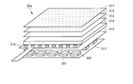
- FIG. 2 is a cross-sectional view of the liquid crystal panel 20.
- the liquid crystal panel 20 has a structure in which a liquid crystal material (not shown) is sandwiched between two glass substrates 201 and 202 (Sp portion in FIG. 2).
- the glass substrate 201 on the back side is provided with a pixel electrode 203, an optical sensor 204, and the like, and the glass substrate 202 on the display surface side is provided with a counter electrode (not shown), a display color filter 205, a black matrix 206, visible light.
- a blocking filter 207 and the like are provided.
- the visible light blocking filter 207 has a characteristic of transmitting infrared light and blocking visible light, and is provided at a position covering the optical sensor 204.
- the visible light blocking filter 207 is formed, for example, by forming a display red color filter and a blue color filter in the same place.
- a light shielding layer 208 is provided on the pixel electrode 203, and the optical sensor 204 is disposed on the light shielding layer 209 provided on the glass substrate 201.
- Polarizing plates 211 and 212 are provided on the surfaces of the glass substrates 201 and 202 that do not face each other, and a protective plate 213 is provided on the display surface side of the liquid crystal panel 20. Air is contained between the glass substrate 202 and the protective plate 213 (Sq portion in FIG. 2).
- FIG. 3 is a diagram showing the arrangement of the sensor pixel circuit 26 in the pixel region 21.
- the (n ⁇ m / 2) sensor pixel circuits 26 include a first sensor pixel circuit 26a that detects light when the infrared backlight 32 is turned on, and a second sensor that detects light when the infrared backlight 32 is turned off. Sensor pixel circuit 26b.
- the number of first sensor pixel circuits 26a and the number of second sensor pixel circuits 26b is the same.
- (n ⁇ m / 4) first sensor pixel circuits 26a are arranged in the vicinity of the intersections of odd-numbered clock lines CLK1 to CLKn-1 and odd-numbered output lines OUT1 to OUTm-1. Is done.
- the (n ⁇ m / 4) second sensor pixel circuits 26b are arranged near the intersections of the even-numbered clock lines CLK2 to CLKn and the even-numbered output lines OUT2 to OUTm.
- the gate driver circuit 22 sequentially selects one gate line from the gate lines GL1 to GLx based on the control signal CSg, and applies a high level potential to the selected gate line. As a result, the y display pixel circuits 25 connected to the selected gate line are collectively selected.
- the source driver circuit 23 applies potentials corresponding to the video signal VS to the source lines SL1 to SLy based on the control signal CSs.
- the potentials applied to the source lines SL1 to SLy are written in y display pixel circuits 25 selected by the gate driver circuit 22.
- a desired image can be displayed on the liquid crystal panel 20 by writing a potential corresponding to the video signal VS to all the display pixel circuits 25.
- the sensor row driver circuit 24 applies a high level potential and a low level potential to the clock lines CLK1 to CLKn based on the control signal CSr (details will be described later). In addition, the sensor row driver circuit 24 applies reset high-level potentials to the odd-numbered reset lines RST1 to RSTn-1 and the even-numbered reset lines RST2 to RSTn at different timings based on the control signal CSr. . Thereby, the first sensor pixel circuit 26a is collectively reset at a certain timing, and the second sensor pixel circuit 26b is collectively reset at another timing.
- the sensor row driver circuit 24 sequentially selects two adjacent read lines from the read lines RWS1 to RWSn based on the control signal CSr, and applies a high level potential for reading to the selected read line.
- the m sensor pixel circuits 26 connected to the two selected readout lines become ready for readout collectively.
- the source driver circuit 23 applies a high level potential to the power supply lines VDD1 to VDDm. Accordingly, signals corresponding to the amount of light detected by each sensor pixel circuit 26 (hereinafter referred to as sensor signals) are output from the m sensor pixel circuits 26 in a readable state to the output lines OUT1 to OUTm.
- the source driver circuit 23 includes a difference circuit (not shown) for obtaining a difference between the output signal of the first sensor pixel circuit 26a and the output signal of the second sensor pixel circuit 26b.
- the source driver circuit 23 amplifies the light amount difference obtained by the difference circuit, and outputs the amplified signal to the outside of the liquid crystal panel 20 as the sensor output Sout. By reading out sensor signals from all the sensor pixel circuits 26 in this way, it is possible to detect light incident on the liquid crystal panel 20.
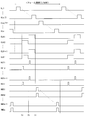
- FIG. 4 is a diagram showing the lighting and extinguishing timings of the infrared backlight 32 and the reset and reading timings of the sensor pixel circuit 26.
- the infrared backlight 32 is lit for a predetermined time once in one frame period, and is turned off in other periods. Specifically, the infrared backlight 32 is turned on at time tb within one frame period and turned off at time tc.
- all the first sensor pixel circuits 26a are reset, and the first sensor pixel circuit 26a detects light incident during a period A1 (lighting period of the infrared backlight 32) from time tb to time tc. .
- all the second sensor pixel circuits 26b are reset at time ta, and the second sensor pixel circuit 26b receives the light incident during the period A2 (the infrared backlight 32 extinguishing period) from time ta to time tb. Detect.
- the period A1 and the period A2 have the same length. Reading from the first sensor pixel circuit 26a and reading from the second sensor pixel circuit 26b are performed in line-sequentially in parallel after time tc.
- the white backlight 31 is turned off during the light detection period A1 of the first sensor pixel circuit 26a and the light detection period A2 of the second sensor pixel circuit 26b, and is turned on otherwise. Specifically, the white backlight 31 is turned off at time ta within one frame period and turned on at time tc.
- FIG. 5 is a circuit diagram of the sensor pixel circuit 26.
- the anode of the photodiode D1a is connected to the reset line RSTa, and the cathode is connected to the source of the transistor T1a.
- the gate of the transistor T1a is connected to the clock line CLKa, and the drain is connected to the gate of the transistor M1a.
- the drain of the transistor M1a is connected to the power supply line VDDa, and the source is connected to the output line OUTa.
- the capacitor C1a is provided between the gate of the transistor M1a and the read line RWSa.
- a node connected to the gate of the transistor M1a serves as an accumulation node that accumulates charges according to the detected light amount.
- the photodiode D1a functions as the optical sensor 204 shown in FIG.
- the second sensor pixel circuit 26b has the same configuration as the first sensor pixel circuit 26a.
- FIG. 6 is a signal waveform diagram of the liquid crystal panel 20.
- the potentials of the gate lines GL1 to GLx are set to the high level for a predetermined time in order once every frame period.
- the odd-numbered clock signals CLK1 to CLKn ⁇ 1 are set to the high level once in one frame period in the period A1 (more specifically, from time tb to slightly before time tc).
- the even-numbered clock signals CLK2 to CLKn are set to the high level once in one frame period in the period A2 (more specifically, from time ta to slightly before time tb).
- the odd-numbered reset signals RST1 to RSTn ⁇ 1 are at a high level once every frame period and for a predetermined time at the beginning of the period A1.
- the even-numbered reset signals RST2 to RSTn are set to the high level once every frame period and for a predetermined time at the beginning of the period A2.
- the read lines RWS1 to RWSn are paired two by two, and the (n / 2) pairs of read signals sequentially go high for a predetermined time after time tc.
- FIG. 7 is a diagram showing the operation of the first sensor pixel circuit 26a. As shown in FIG. 7, the first sensor pixel circuit 26a performs (a) reset, (b) accumulation, (c) holding, and (d) reading in one frame period. The second sensor pixel circuit 26b operates in the same manner as the first sensor pixel circuit 26a.
- FIG. 8 is a signal waveform diagram of the sensor pixel circuit 26.
- W-BL represents the luminance of the white backlight
- Ir-BL represents the luminance of the infrared backlight 32
- Vinta represents the potential of the storage node of the first sensor pixel circuit 26a
- Vintb represents the first. This represents the potential of the storage node of the two-sensor pixel circuit 26b.
- the reset period is from time t4 to time t5
- the accumulation period is from time t5 to time t6
- the holding period is from time t6 to time t7
- the readout period is from time t7 to time t8.
- the time t1 to time t2 is a reset period
- the time t2 to time t3 is an accumulation period
- the time t3 to time t7 is a holding period
- the time t7 to time t8 is a reading period.
- the clock signal CLKa is at a high level
- the readout signal RWSa is at a low level
- the reset signal RSTa is at a reset high level.
- the transistor T1a is turned on. Therefore, a current flows from the reset line RSTa to the storage node via the photodiode D1a and the transistor T1a (FIG. 7A), and the potential Vanta is reset to a predetermined level.
- the clock signal CLKa is at a high level, and the reset signal RSTa and the readout signal RWSa are at a low level.
- the transistor T1a is turned on.
- a current flows from the storage node to the reset line RSTa via the transistor T1a and the photodiode D1a, and charges are extracted from the storage node (FIG. 7B). Accordingly, the potential Vanta drops according to the amount of light incident during the period when the clock signal CLKa is at the high level.
- the clock signal CLKa, the reset signal RSTa, and the readout signal RWSa are at a low level. At this time, the transistor T1a is turned off. At this time, even if light is incident on the photodiode D1a, the transistor T1a is turned off, so that the potential Vanta does not change (FIG. 7C).
- the clock signal CLKa and the reset signal RSTa are at a low level, and the readout signal RWSa is at a readout high level.
- the transistor T1a is turned off.
- the potential Vanta increases by (Cqa / Cpa) times the amount of increase in the potential of the readout signal RWSa (where Cpa is the overall capacitance value of the first sensor pixel circuit 26a and Cqa is the capacitance value of the capacitor C1a).
- the transistor M1a forms a source follower amplifier circuit using a transistor (not shown) included in the source driver circuit 23 as a load, and drives the output line OUTa according to the potential Vanta (FIG. 7D).
- the sensor signal corresponding to the amount of light incident while the clock signal CLKa is at the high level (the detection period when the infrared backlight 32 is lit) is read out from the first sensor pixel circuit 26a.
- a sensor signal corresponding to the amount of light incident while the clock signal CLKb is at a high level is read from the second sensor pixel circuit 26b.
- FIGS. 9A to 9F are diagrams showing a configuration example of the backlight 30.
- the backlights 30a to 30f shown in FIGS. 9A to 9F include a white LED (Light (Emitting Diode) 301 that emits white light and an infrared LED 302 that emits infrared light.
- white LED Light (Emitting Diode) 301 that emits white light
- infrared LED 302 that emits infrared light.
- all white LEDs 301 are lit when the control signal CSb1 is at a high level
- all infrared LEDs 302 are lit when the control signal CSb2 is at a high level.
- the backlight 30 a shown in FIG. 9A two lens sheets 311 and 312 and a diffusion sheet 313 are provided on one surface of the light guide plate 314, and a reflection sheet 315 is provided on the other surface of the light guide plate 314. .
- a flexible printed circuit board 316 in which white LEDs 301 are arranged one-dimensionally is provided on the side surface of the light guide plate 314.
- a circuit board 317 in which infrared LEDs 302 are two-dimensionally arranged is provided.
- the reflection sheet 315 a sheet that transmits infrared light and reflects visible light is used.
- the light guide plate 321 and the reflection sheet 323 are provided on the side of the light guide plate 314 where the reflection sheet 315 is provided.
- a flexible printed circuit board 322 in which infrared LEDs 302 are arranged one-dimensionally is provided on the side surface of the light guide plate 321.
- the reflection sheet 323 a material that reflects infrared light is used.
- a flexible printed circuit board 331 in which white LEDs 301 and infrared LEDs 302 are mixedly arranged in a one-dimensional manner is provided on the side surface of the light guide plate 314.
- a reflection sheet 332 that reflects visible light and infrared light is provided on the surface of the light guide plate 314 on which the diffusion sheet 313 is not provided.
- 9D includes a circuit board 341 in which white LEDs 301 and infrared LEDs 302 are two-dimensionally mixed. Two lens sheets 311 and 312 and a diffusion sheet 313 are provided on one surface of the circuit board 341, and a reflection sheet 332 is provided on the other surface.
- a flexible printed circuit board 352 in which a white LED 301 and an infrared LED 302 are sealed together in the same resin package 351 is arranged one-dimensionally and provided on the side surface of the light guide plate 314. Yes.
- a flexible printed board 316 in which white LEDs 301 are arranged one-dimensionally is provided on one side surface of the light guide plate 361, and a flexible printed board 362 in which infrared LEDs 302 are arranged one-dimensionally is guided. It is provided on the opposite side surface of the light plate 361.
- FIG. 9G is a cross-sectional view of the backlight 30f.
- the light guide plate 361 is processed so that both white light incident from one side surface and infrared light incident from the opposite side surface propagate.
- the periods A1 and A2 are set to have the same length once every frame period, and the sensor pixel circuit 26 detects the first light in the period A1.
- a sensor pixel circuit 26a and a second sensor pixel circuit 26b that detects light in the period A2 are included.
- the white backlight 31 is turned off entirely during the periods A1 and A2, and is turned on all other times.
- the entire infrared backlight 32 is turned on during the period A1, and is turned off during all other periods.
- the liquid crystal display device according to the present embodiment is characterized in that the white backlight 31 is turned off corresponding to the photosensor 204 that is detecting light.
- a part of the light emitted from the backlight 30 is part of the surface of the protective plate 213 (lights La and Lb), the interface between the polarizing plate 212 on the display surface side and air (light Lc), or , Reflected by the pixel electrode 203 (light Lx) and incident on the optical sensor 204.
- Visible light included in the light La to Lc is blocked by the visible light blocking filter 207 or the like, and thus does not reach the optical sensor 204.
- visible light included in the light Lx reaches the optical sensor 204 without being blocked by the visible light blocking filter 207.
- the white backlight 31 is turned off corresponding to the light sensor 204 that is detecting light. Specifically, the white backlight 31 is turned off entirely during the period A1 during which the first sensor pixel circuit 26a detects light and during the period A2 during which the second sensor pixel circuit 26b detects light. For this reason, the backlight for display is not reflected inside the liquid crystal panel 20 and is not incident on the photosensor 204 during light detection. Therefore, according to the liquid crystal display device according to the present embodiment, the effective area of the optical sensor 204 can be widened. Thereby, the illuminance range in which the touch position can be detected can be widened.
- FIG. 10 is a diagram showing an effective area of an optical sensor formed of polysilicon, microcrystalline silicon, and amorphous silicon.
- the optical sensor needs to be used within a range (linear region) where the output (detected light amount) changes linearly according to the input (incident light amount).
- the three types of optical sensors detect light amounts in the same range (0 to 1023 gradations), have linear regions in the same range (246 to 717 gradations), and have the same sensitivity to infrared light. Shall have.
- the optical sensor is obtained by subtracting the reflected light amount of the white backlight light and the reflected light amount of the infrared backlight light from the linear region of the optical sensor. Can be obtained.
- the amount of reflected light of white backlight light corresponds to 8 gradations
- the amount of reflected light of infrared backlight light corresponds to 55 gradations.
- the sensitivity of an optical sensor made of amorphous silicon to visible light is about 100 times that of an optical sensor made of polysilicon. For this reason, in the optical sensor formed of amorphous silicon, the amount of reflected light of the white backlight corresponds to 800 gradations. If the amount of reflected light of white backlight light and the amount of reflected light of infrared backlight light are subtracted from the linear region of the optical sensor, the result is negative. Therefore, the optical sensor formed of amorphous silicon does not have an effective area.
- the optical sensor is formed of amorphous silicon
- the output of the optical sensor is saturated when the white backlight light is reflected inside the liquid crystal panel and even enters the optical sensor. Therefore, in the conventional liquid crystal display device, it is extremely difficult to use an optical sensor formed of amorphous silicon when using infrared light for detecting the touch position.
- the white backlight 31 is extinguished corresponding to the light sensor 204 that is detecting light, so that the visible light emitted from the white backlight 31 is being detected. It does not enter the optical sensor 204. Therefore, even when the optical sensor 204 is formed of amorphous silicon, it is possible to secure an effective area of the optical sensor 204 and widen the illuminance range in which the touch position can be detected.
- This amount of light corresponds to 25 gradations in the photosensor formed of microcrystalline silicon, and corresponds to 250 gradations in the photosensor formed of amorphous silicon. Therefore, when the photosensor is formed of amorphous silicon, the effective area of the photosensor can be ensured even when the reflected light from the backlight of external light is taken into consideration.
- the liquid crystal display device As described above, according to the liquid crystal display device according to the present embodiment, visible light emitted from the white backlight is being detected by the white backlight being extinguished in response to the photosensor being detected. Can be prevented, and the effective area of the optical sensor can be widened. Further, by detecting the light amount when the infrared backlight is turned on and the light amount when the infrared backlight is turned off, the difference between the two can be obtained, and an input image that is not affected by external light can be obtained. Further, each backlight can be easily configured by using a white backlight that is turned on / off entirely and an infrared backlight that is turned on / off completely. In addition, when the white backlight is completely turned off in a predetermined period of one frame period, the moving image display quality can be improved as in the case of inserting a black image.
- the liquid crystal display device according to the second embodiment of the present invention has the same configuration as the liquid crystal display device according to the first embodiment, and operates in the same manner (see FIGS. 1 to 8).
- the liquid crystal display device according to the present embodiment relates to the first embodiment in which at least one of the two types of backlights is partially lit / partially turned off, and both of the two types of backlights are turned on / off entirely. Different from the liquid crystal display device.
- differences between the present embodiment and the first embodiment will be described.
- the backlight 30 includes a white backlight 31 that is turned on / off entirely and an infrared backlight 32 that can be partially turned on (type A), and has a white backlight 31 that can be turned off and full turn on / off. It has either a configuration including an infrared backlight 32 that turns off the entire surface (B type) or a configuration including a white backlight 31 that can be partially turned off and an infrared backlight 32 that can be partially turned on (C type).
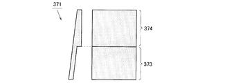
- the tandem-type backlight is configured by arranging a plurality of tandem light guide plates 371 in a two-dimensional manner and providing an LED 372 for each tandem light guide plate 371 (FIGS. 11A and 11B).
- the tandem light guide plate 371 includes a light guide portion 373 and a light emitting portion 374 (FIG. 11C).
- the tandem light guide plate 371 is arranged so that the light emitting part 374 forms one plane, and the LED 372 is provided at the end of the light guide part 373.
- the backlights 30a to 30f shown in FIGS. 9A to 9F, or modified versions thereof are used.
- a backlight 30a is used.
- the backlight 30a, 30b in which the white backlight 31 is tandem-type is used.
- the backlight 30a in which the white LED 301 and the infrared LED 302 are arranged in reverse may be used. In the latter case, a material that transmits visible light and reflects infrared light is used as the reflection sheet 315.
- a backlight 30d is used for the C-type backlight 30, for example.
- the backlight 30a in which the white backlight 31 is tandem type or the backlights 30b, 30c, 30e, and 30f in which two types of backlights are tandem type may be used.
- the display control circuit 10 When using the white backlight 31 that can be partially turned off, the display control circuit 10 outputs a plurality of control signals CSb 1, and each control signal CSb 1 is associated with one or a plurality of white LEDs 301.
- the white backlight 31 is partially turned off according to a plurality of control signals CSb1.
- the display control circuit 10 When the partially lit infrared backlight 32 is used, the display control circuit 10 outputs a plurality of control signals CSb 2, and each control signal CSb 2 is associated with one or a plurality of infrared LEDs 302.
- the infrared backlight 32 is partially lit in accordance with a plurality of control signals CSb2.
- FIG. 12 is a diagram showing an example of a display screen of the liquid crystal display device according to the present embodiment.
- two buttons 42a and 42b are displayed together with the image of the car.
- detection areas 43a and 43b are set on the display screen 41 in the vicinity of the buttons 42a and 42b.
- the positions of the detection areas 43a and 43b change according to display contents. Note that the position of the detection region may be fixed regardless of the display content.
- the white backlight 31 is turned off in the period A1 (light detection period of the first sensor pixel circuit 26a) and the period A2 (light detection period of the second sensor pixel circuit 26b). Otherwise, it lights up.
- the infrared backlight 32 is turned on during the period A1, and is turned off during other periods.
- the white backlight 31 has a function of partially turning off
- the white backlight 31 is partially turned off corresponding to the detection area in the periods A1 and A2.
- the infrared backlight 32 has a function of partially lighting
- the infrared backlight 32 is partially lit corresponding to the detection area in the period A1. For example, when the display screen 41 shown in FIG.
- the white backlight 31 that can be partially turned off is partially turned off corresponding to the detection areas 43a and 43b, and the infrared backlight 32 that can be partially turned on is the detection area. Partial lighting is performed corresponding to 43a and 43b.
- the white backlight 31 that is partially turned off corresponding to the detection area set on the display screen in the periods A1 and A2, and the display screen is set in the period A1.
- An infrared backlight 32 that is partially lit corresponding to the detection region, or both, is provided. Since the white backlight 31 is partially turned off corresponding to the detection area, the white backlight 31 is turned on in the area other than the detection area to perform display, and the influence on the display can be reduced. In addition, since the infrared backlight 32 is partially lit corresponding to the detection region, the power consumption of the infrared backlight 32 can be reduced.
- the liquid crystal display device As a first application example, there is a method of switching the size of the detection region in accordance with the size of the detection target (finger, pen, etc.) (see FIG. 13).
- the size of the detection target in the input image obtained using the optical sensor may be known. For example, it is assumed that the finger size in the input image is (30 ⁇ 30) pixels and the pen size is (8 ⁇ 8) pixels.
- a detection area 44 having the same size as the (30 ⁇ 30) sensor pixel circuits is set, and the white backlight 31 is partially turned off corresponding to the detection area 44, and the infrared backlight 32 is partially lit corresponding to the detection area 44 (FIG. 13A).
- a detection area 45 having the same size as (8 ⁇ 8) sensor pixel circuits is set, the white backlight 31 is partially turned off corresponding to the detection area 45, and the infrared backlight 32 is detected. Partial lighting is performed corresponding to the region 45 (FIG. 13B).
- FIG. 14 there is a method of setting a detection area when a detection object approaches a liquid crystal panel (see FIG. 14).
- the white backlight 31 is completely turned off for a predetermined period, and the infrared backlight 32 is turned on for a predetermined period (FIG. 14A).
- a detection area 47 corresponding to the size and position of the detection target is set on the display screen 46 (FIG. 14B).
- the white backlight 31 is partially turned off corresponding to the detection area 47, and the infrared backlight 32 is partially turned on corresponding to the detection area 47.
- the white backlight 31 is completely turned off during the light detection period, and is completely turned off except during the light detection period, and the infrared backlight 32 is partially turned on in the vicinity of the button 49 during the light detection period, except for the light detection period. Then turn off the entire surface. In the latter case, the white backlight 31 is partially lit in the vicinity of the button 49 except during the light detection period. Thereby, the power consumption of a backlight can be reduced.
- the liquid crystal display device according to the third embodiment of the present invention has the same configuration as the liquid crystal display device according to the first embodiment (see FIG. 1).
- the liquid crystal display device according to the first embodiment uses two types of sensor pixel circuits 26 to detect the amount of light when the infrared backlight 32 is turned on and the amount of light when the infrared backlight 32 is turned off.
- the liquid crystal display device according to the present embodiment detects the amount of light when the infrared backlight 32 is turned on using one type of sensor pixel circuit 26.
- FIG. 16 is a diagram showing the arrangement of the sensor pixel circuit 26 in the pixel region 21.
- (n ⁇ m / 2) sensor pixel circuits 26c are provided in the pixel region 21 according to the present embodiment.
- the (n ⁇ m / 2) sensor pixel circuits 26c include the odd-numbered clock lines CLK1 to CLKn-1 and the odd-numbered output lines OUT1 to OUTm ⁇ 1 in the vicinity of the intersection and the even-numbered ones.
- the clock lines CLK2 to CLKn and the even-numbered output lines OUT2 to OUTm are arranged in the vicinity of the intersections.
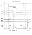
- FIG. 17 is a diagram showing the writing timing for the display pixel circuit 25, the lighting and extinguishing timing of the white backlight 31, and the reset and reading timing for the sensor pixel circuit 26c.
- the sensor pixel circuit 26c is reset line-sequentially once per frame period. More specifically, the sensor pixel circuit 26c in the first row is reset at the beginning of one frame period, then the sensor pixel circuit 26c in the second row is reset, and then the sensor pixels in the third row and thereafter. The circuit 26c is reset in order.
- Reading from the sensor pixel circuit 26c in the i-th row (i is an integer of 1 or more and n or less) is performed after a predetermined time has elapsed since the reset to the sensor pixel circuit 26c in the i-th row.
- the period from reset to readout is the light detection period.
- the sensor pixel circuit 26c in the i-th row is reset at time td, and reading from the sensor pixel circuit 26c in the i-th row is performed at time te.
- the sensor pixel circuit 26c in the i-th row detects light in a period Bi from time td to time te.
- FIG. 18 is a diagram showing a light detection range by the optical sensor 204.
- the light detection range by the photosensor 204 becomes a band-like region 51 shown in FIG.
- the band-like area 51 moves downward in the display screen.
- the white backlight 31 is partially extinguished corresponding to the band-like region 51 shown in FIG.
- a white backlight 31 can be configured, for example, by the same method as in the second embodiment.
- a plurality of cold cathode tubes may be arranged side by side and turned off in order.
- the infrared backlight 32 is always turned on. Writing to the display pixel circuit 25 is performed on a portion where the white backlight 31 is newly turned off as shown in FIG.
- FIG. 19 is a circuit diagram of the sensor pixel circuit 26c.
- the anode of the photodiode D1 is connected to the reset line RST, and the cathode is connected to the gate of the transistor M1.
- the drain of the transistor M1 is connected to the power supply line VDD, and the source is connected to the output line OUT.
- a node connected to the gate of the transistor M1 serves as an accumulation node for accumulating charges according to the detected light amount.
- the photodiode D1 functions as the optical sensor 204. Since the sensor pixel circuit 26c is not connected to the readout line, it is not necessary to provide the readout line in the liquid crystal panel 20 according to the present embodiment.
- the white backlight 31 is partially extinguished corresponding to the band-like area 51 moving in the predetermined direction within the display screen, and the optical sensor 204 corresponding to the band-like area 51. Detects light. As described above, also in the present embodiment, the white backlight 31 is turned off corresponding to the light sensor that is detecting light. Therefore, also in this embodiment, similarly to the first embodiment, visible light emitted from the white backlight can be prevented from entering the photosensor that is detecting light, and the effective area of the photosensor can be widened. .
- the infrared backlight 32 is always turned on. Thereby, the infrared backlight 32 can be configured easily. Instead of this, the infrared backlight 32 may be partially lit corresponding to the band-like region 51. Thereby, the power consumption of the infrared backlight 32 can be reduced.
- the second embodiment is applied to the present embodiment, the white backlight is partially turned off corresponding to the detection area set as the display area, and the infrared backlight is the detection area set as the display area. Partial lighting may be performed in response to.
- the number of sensor pixel circuits 26 provided in the pixel region 21 may be arbitrary.
- the visible light blocking filter 207 an RGB filter in which a display red color filter, a green color filter and a blue filter are overlapped is used instead of a BR filter formed by overlapping a display red color filter and a blue filter. Also good.
- FIG. 20 is a diagram illustrating spectral characteristics of the BR filter and the RGB filter. By using the RGB filter, visible light incident on the optical sensor can be better blocked.
- the optical sensor can be formed using polysilicon, microcrystalline silicon, amorphous silicon, or the like. Since these materials have different crystallinity, the optical sensor formed of each material has different sensitivity characteristics. Since the optical sensor formed of polysilicon has a wide linear region, it can be applied to usage forms that require a wide effective region (for example, mobile use). An optical sensor formed of microcrystalline silicon has high sensitivity to some extent and a wide linear region to some extent, and can be applied to various usage forms. Since an optical sensor formed of amorphous silicon has high sensitivity, it can be applied to usage forms that require high sensitivity.
- the display device with an optical sensor of the present invention has a feature that the effective area of the optical sensor is wide, and thus can be used for various display devices such as a liquid crystal display device with an optical sensor.
- DESCRIPTION OF SYMBOLS 10 ... Display control circuit 20 ... Liquid crystal panel 21 ... Pixel area 22 ... Gate driver circuit 23 ... Source driver circuit 24 ... Sensor row driver circuit 25 ... Display pixel circuit 26 ... Sensor pixel circuit 30 ... Backlight 31 ... White backlight 32 ... Infrared backlight 43, 44, 45, 47 ... detection area 51 ... band-like area 204 ... optical sensor 207 ... visible light blocking filter
Abstract
液晶表示装置は、複数の光センサを含む液晶パネル20、白色バックライト31、および、赤外バックライト32を備えている。赤外バックライト32は、所定のタイミングで点灯および消灯する。光センサの一部は赤外バックライト32の点灯時に光を検知し、他の一部は赤外バックライト32の消灯時に光を検知する。白色バックライト31は、光検知中の光センサに対応して消灯する。これにより、表示装置に含まれる光センサの有効領域を広くする。
Description
本発明は、表示装置に関し、特に、表示パネルに複数の光センサを設けた光センサ付き表示装置に関する。
近年、指やペンなどで画面に触れることにより操作可能な電子機器が普及している。また、表示画面内のタッチ位置を検出する方法として、表示パネルに複数の光センサを設け、光センサを用いて得られた入力画像に対して画像処理を行う方法が知られている。このような光センサ付き表示装置には、外光の影響を受けずに高い精度でタッチ位置を検出することが要求される。
タッチ位置の検出精度を高くする方法は、従来から各種考案されている。例えば特許文献1には、赤外光を出射するバックライトを設ける方法が記載されており、特許文献2には、光センサへの光入射経路上に赤外光を透過し可視光を遮断するフィルタを設ける方法が記載されている。また、特許文献3には、あるタイミングで黒画像を表示し、別のタイミングで黒画像よりも高い輝度を有する画像(例えば、青画像)を表示する方法が記載されている。さらに特許文献4には、非可視光を発光する第1の発光手段と、可視光を発光する第2の発光手段とを設け、2個の発光手段の発光制御を並列的に実行する方法が記載されている。
一般に、バックライトを備えた表示装置では、バックライトから出射された光(バックライト光)は、表示パネルの内部で反射する。バックライト光は、例えば、画素電極、偏光板、保護板などで反射する。このため、赤外バックライトと可視光遮断フィルタを備えた光センサ付き表示装置では、表示用のバックライト光(可視光)の一部がノイズとして光センサに入射し、タッチ位置の検出に必要な光センサの有効領域(利用可能な光量の範囲)が狭くなることが問題になることがある。
この問題は、光センサをアモルファスシリコンで形成する場合に顕著になる。図21は、ポリシリコン、微結晶シリコンおよびアモルファスシリコンで形成した光センサの分光感度特性を示す図である。図21に示すように、波長850nmのときの感度と波長550nmのときの感度の比は、ポリシリコンで形成した光センサでは約1:100であり、アモルファスシリコンで形成した光センサでは約1:10000である。このため、赤外光に対する感度が同程度になるように、ポリシリコンとアモルファスシリコンで光センサを形成した場合、アモルファスシリコンで形成した光センサの白色光に対する感度は、ポリシリコンで形成した光センサの約100倍になる。したがって、光センサをアモルファスシリコンで形成した場合、白色バックライト光が表示パネルの内部で反射して光センサにわずかでも入射すると、光センサの出力が飽和する。このような理由により、タッチ位置の検出に赤外光を使用する場合に、アモルファスシリコンで形成した光センサを使用することは、極めて困難である。
特許文献1~4に記載された従来の光センサ付き表示装置でも、バックライト光が表示パネルの内部で反射して光センサに入射し、光センサの有効領域が狭くなるという問題を解決することはできない。
それ故に、本発明は、光センサの有効領域が広い光センサ付き表示装置を提供することを目的とする。
本発明の第1の局面は、複数の光センサを備えた表示装置であって、
2次元状に配置された複数の光センサを含む表示パネルと、
可視光を出射する第1の光源と、
赤外光を出射する第2の光源と、
前記光センサへの光入射経路上に設けられ、赤外光を透過し可視光を遮断するフィルタとを備え、
前記第1の光源は、光検知中の光センサに対応して消灯することを特徴とする。
2次元状に配置された複数の光センサを含む表示パネルと、
可視光を出射する第1の光源と、
赤外光を出射する第2の光源と、
前記光センサへの光入射経路上に設けられ、赤外光を透過し可視光を遮断するフィルタとを備え、
前記第1の光源は、光検知中の光センサに対応して消灯することを特徴とする。
本発明の第2の局面は、本発明の第1の局面において、
前記光センサには、第1検知期間で光を検知するものと、第2検知期間で光を検知するものとが含まれており、
前記第1の光源は、前記第1および第2検知期間では光検知中の光センサを含む範囲に対応して消灯し、
前記第2の光源は、前記第1検知期間では光検知中の光センサを含む範囲に対応して点灯し、前記第2検知期間では全面消灯することを特徴とする。
前記光センサには、第1検知期間で光を検知するものと、第2検知期間で光を検知するものとが含まれており、
前記第1の光源は、前記第1および第2検知期間では光検知中の光センサを含む範囲に対応して消灯し、
前記第2の光源は、前記第1検知期間では光検知中の光センサを含む範囲に対応して点灯し、前記第2検知期間では全面消灯することを特徴とする。
本発明の第3の局面は、本発明の第2の局面において、
前記第1および第2検知期間は、1フレーム期間に1回ずつ同じ長さで設定されていることを特徴とする。
前記第1および第2検知期間は、1フレーム期間に1回ずつ同じ長さで設定されていることを特徴とする。
本発明の第4の局面は、本発明の第2の局面において、
前記第1の光源は、前記第1および第2検知期間では全面消灯することを特徴とする。
前記第1の光源は、前記第1および第2検知期間では全面消灯することを特徴とする。
本発明の第5の局面は、本発明の第2の局面において、
前記第2の光源は、前記第1検知期間では全面点灯することを特徴とする。
前記第2の光源は、前記第1検知期間では全面点灯することを特徴とする。
本発明の第6の局面は、本発明の第2の局面において、
前記第1の光源は、前記第1および第2検知期間では表示画面に設定された検知領域に対応して部分消灯することを特徴とする。
前記第1の光源は、前記第1および第2検知期間では表示画面に設定された検知領域に対応して部分消灯することを特徴とする。
本発明の第7の局面は、本発明の第2の局面において、
前記第2の光源は、前記第1検知期間では表示画面に設定された検知領域に対応して部分点灯することを特徴とする。
前記第2の光源は、前記第1検知期間では表示画面に設定された検知領域に対応して部分点灯することを特徴とする。
本発明の第8の局面は、本発明の第6または第7の局面において、
前記検知領域は、検知対象物に応じたサイズを有することを特徴とする。
前記検知領域は、検知対象物に応じたサイズを有することを特徴とする。
本発明の第9の局面は、本発明の第6または第7の局面において、
前記検知領域は、検知対象物が前記表示パネルに接近したときに設定されることを特徴とする。
前記検知領域は、検知対象物が前記表示パネルに接近したときに設定されることを特徴とする。
本発明の第10の局面は、本発明の第1の局面において、
前記第1の光源は、表示画面内を所定方向に移動する帯状領域に対応して部分消灯し、
前記帯状領域に対応する光センサが、光を検知することを特徴とする。
前記第1の光源は、表示画面内を所定方向に移動する帯状領域に対応して部分消灯し、
前記帯状領域に対応する光センサが、光を検知することを特徴とする。
本発明の第11の局面は、本発明の第10の局面において、
前記第2の光源は、全面点灯することを特徴とする。
前記第2の光源は、全面点灯することを特徴とする。
本発明の第12の局面は、本発明の第10の局面において、
前記第2の光源は、前記帯状領域に対応して部分点灯することを特徴とする。
前記第2の光源は、前記帯状領域に対応して部分点灯することを特徴とする。
本発明の第13の局面は、本発明の第1の局面において、
前記光センサがアモルファスシリコンで形成されていることを特徴とする。
前記光センサがアモルファスシリコンで形成されていることを特徴とする。
本発明の第14の局面は、本発明の第1の局面において、
前記光センサが微結晶シリコンで形成されていることを特徴とする。
前記光センサが微結晶シリコンで形成されていることを特徴とする。
本発明の第15の局面は、本発明の第1の局面において、
前記光センサがポリシリコンで形成されていることを特徴とする。
前記光センサがポリシリコンで形成されていることを特徴とする。
本発明の第1の局面によれば、第1の光源が光検知中の光センサに対応して消灯することにより、第1の光源から出射された可視光が光検知中の光センサに入射することを防止し、光センサの有効領域を広くすることができる。
本発明の第2の局面によれば、第2の光源点灯時の光量と第2の光源消灯時の光量を検知することにより、両者の差を求めて、外光の影響を受けない入力画像を得ることができる。また、第1の光源が第1および第2の検知期間で光検知中の光センサを含む範囲に対応して消灯することにより、第1の光源から出射された可視光が光検知中の光センサに入射することを防止し、光センサの有効範囲を広くすることができる。
本発明の第3の局面によれば、第1および第2の検知期間を1フレーム期間に1回ずつ同じ長さで設定することにより、外光の影響を受けない入力画像をフレーム期間ごとに得ることができる。
本発明の第4の局面によれば、第1の光源を容易に構成することができる。
本発明の第5の局面によれば、第2の光源を容易に構成することができる。
本発明の第6の局面によれば、第1の光源が検知領域に対応して部分消灯することにより、検知領域以外では第1の光源を点灯させて表示を行い、表示に与える影響を減らすことができる。
本発明の第7の局面によれば、第2の光源が検知領域に対応して部分点灯することにより、第2の光源の消費電力を減らすことができる。
本発明の第8の局面によれば、検知対象物に応じて検知領域のサイズを切り替えることにより、表示に与える影響や第2の光源の消費電力を検知対象物に応じて好適に減らすことができる。
本発明の第9の局面によれば、検知対象物が表示パネルに接近したときに検知領域を設定することにより、表示に与える影響や第2の光源の消費電力を検知対象物と表示パネルの間の距離に応じて好適に減らすことができる。
本発明の第10の局面によれば、第1の光源が帯状領域に対応して消灯し、帯状領域に対応する光センサが光を検知することにより、第1の光源から出射された可視光が光検知中の光センサに入射することを防止し、光センサの有効範囲を広くすることができる。
本発明の第11の局面によれば、第2の光源を容易に構成することができる。
本発明の第12の局面によれば、第2の光源が帯状領域に対応して部分消灯することにより、第2の光源の消費電力を減らすことができる。
本発明の第13の局面によれば、光センサをアモルファスシリコンで形成することにより、光センサの感度を高くして、高い感度を必要とする利用形態に適用することができる。
本発明の第14の局面によれば、光センサを微結晶シリコンで形成することにより、感度がある程度高く、線形領域がある程度広い光センサを形成し、各種の利用形態に適用することができる。
本発明の第15の局面によれば、光センサをポリシリコンで形成することにより、光センサの線形領域を広くして、広い有効領域を必要とする利用形態に適用することができる。
(第1の実施形態)
図1は、本発明の第1の実施形態に係る液晶表示装置の構成を示すブロック図である。図1に示す液晶表示装置は、表示制御回路10、液晶パネル20、および、バックライト30を備えている。この液晶表示装置は、液晶パネル20に画像を表示する機能と、液晶パネル20に入射した光を検知する機能とを有する。以下、xおよびyを2以上の整数、mおよびnを偶数とし、液晶表示装置のフレームレートを60フレーム/秒とする。また、信号線上の信号を識別するために信号線と同じ名称を使用する(例えば、クロック線CLK上の信号をクロック信号CLKという)。
図1は、本発明の第1の実施形態に係る液晶表示装置の構成を示すブロック図である。図1に示す液晶表示装置は、表示制御回路10、液晶パネル20、および、バックライト30を備えている。この液晶表示装置は、液晶パネル20に画像を表示する機能と、液晶パネル20に入射した光を検知する機能とを有する。以下、xおよびyを2以上の整数、mおよびnを偶数とし、液晶表示装置のフレームレートを60フレーム/秒とする。また、信号線上の信号を識別するために信号線と同じ名称を使用する(例えば、クロック線CLK上の信号をクロック信号CLKという)。
図1に示す液晶表示装置には外部から、映像信号Vinとタイミング制御信号Cinが供給される。表示制御回路10は、これらの信号に基づき、液晶パネル20に対して映像信号VSと制御信号CSg、CSs、CSrを出力し、バックライト30に対して制御信号CSb1、CSb2を出力する。映像信号VSは、映像信号Vinと同じでもよく、映像信号Vinに信号処理を施した信号でもよい。
バックライト30は、液晶パネル20の背面側に設けられ、液晶パネル20の背面に光を照射する。バックライト30には、表示用に白色光(可視光)を出射する白色バックライト31と、光検知用に赤外光を出射する赤外バックライト32とが含まれる。白色バックライト31は第1の光源として機能し、赤外バックライト32は第2の光源として機能する。白色バックライト31は制御信号CSb1がハイレベルのときに点灯し、赤外バックライト32は制御信号CSb2がハイレベルのときに点灯する。
液晶パネル20は、画素領域21、ゲートドライバ回路22、ソースドライバ回路23、および、センサロウドライバ回路24を含んでいる。画素領域21には、x本のゲート線GL1~GLx、y本のソース線SL1~SLy、(x×y)個の表示画素回路25、および、(n×m/2)個のセンサ画素回路26が設けられる。ゲート線GL1~GLxは互いに平行に配置され、ソース線SL1~SLyはゲート線GL1~GLxと直交するように互いに平行に配置される。(x×y)個の表示画素回路25は、ゲート線GL1~GLxとソース線SL1~SLyの交点近傍に配置される。
画素領域21には、ゲート線GL1~GLxと平行に、n本のクロック線CLK1~CLKn、n本のリセット線RST1~RSTn、および、n本の読み出し線RWS1~RWSnが設けられる。センサ画素回路26から読み出しを行うときには、ソース線SL1~SLyの中から選択されたm本が電源線VDD1~VDDmとして使用され、別のm本が出力線OUT1~OUTmとして使用される。
図2は、液晶パネル20の断面図である。図2に示すように、液晶パネル20は、2枚のガラス基板201、202の間(図2のSp部)に液晶物質(図示せず)を挟み込んだ構造を有する。背面側のガラス基板201には画素電極203や光センサ204などが設けられ、表示面側のガラス基板202には対向電極(図示せず)、表示用のカラーフィルタ205、ブラックマトリクス206、可視光遮断フィルタ207などが設けられる。可視光遮断フィルタ207は、赤外光を透過し可視光を遮断する特性を有し、光センサ204を覆う位置に設けられる。可視光遮断フィルタ207は、例えば、表示用の赤色カラーフィルタと青色カラーフィルタを同じ場所に形成することにより形成される。
光センサ204に不要な光が入射することを防止するために、画素電極203上には遮光層208が設けられ、光センサ204はガラス基板201上に設けた遮光層209の上に配置される。ガラス基板201、202の対向しない面には偏光板211、212がそれぞれ設けられ、液晶パネル20の表示面側には保護板213が設けられる。ガラス基板202と保護板213の間(図2のSq部)には、空気が入っている。
図3は、画素領域21におけるセンサ画素回路26の配置を示す図である。(n×m/2)個のセンサ画素回路26には、赤外バックライト32の点灯時に光を検知する第1センサ画素回路26aと、赤外バックライト32の消灯時に光を検知する第2センサ画素回路26bとが含まれる。第1センサ画素回路26aと第2センサ画素回路26bは同数である。図3に示すように、(n×m/4)個の第1センサ画素回路26aは、奇数番目のクロック線CLK1~CLKn-1と奇数番目の出力線OUT1~OUTm-1の交点近傍に配置される。(n×m/4)個の第2センサ画素回路26bは、偶数番目のクロック線CLK2~CLKnと偶数番目の出力線OUT2~OUTmの交点近傍に配置される。
ゲートドライバ回路22は、制御信号CSgに基づき、ゲート線GL1~GLxの中から1本のゲート線を順に選択し、選択したゲート線にハイレベル電位を印加する。これにより、選択されたゲート線に接続されたy個の表示画素回路25が、一括して選択される。ソースドライバ回路23は、制御信号CSsに基づき、映像信号VSに応じた電位をソース線SL1~SLyに印加する。ソース線SL1~SLyに印加された電位は、ゲートドライバ回路22によって選択されたy個の表示画素回路25に書き込まれる。このようにしてすべての表示画素回路25に映像信号VSに応じた電位を書き込むことにより、液晶パネル20に所望の画像を表示することができる。
センサロウドライバ回路24は、制御信号CSrに基づき、クロック線CLK1~CLKnに対してハイレベル電位とローレベル電位を印加する(詳細は後述)。また、センサロウドライバ回路24は、制御信号CSrに基づき、奇数番目のリセット線RST1~RSTn-1と偶数番目のリセット線RST2~RSTnに対して、異なるタイミングでリセット用のハイレベル電位を印加する。これにより、第1センサ画素回路26aはあるタイミングで一括してリセットされ、第2センサ画素回路26bは別のタイミングで一括してリセットされる。
また、センサロウドライバ回路24は、制御信号CSrに基づき、読み出し線RWS1~RWSnの中から隣接する2本の読み出し線を順に選択し、選択した読み出し線に読み出し用のハイレベル電位を印加する。これにより、選択された2本の読み出し線に接続されたm個のセンサ画素回路26が、一括して読み出し可能状態になる。このときソースドライバ回路23は、電源線VDD1~VDDmに対してハイレベル電位を印加する。これにより、読み出し可能状態にあるm個のセンサ画素回路26から出力線OUT1~OUTmに、各センサ画素回路26で検知した光の量に応じた信号(以下、センサ信号という)が出力される。
ソースドライバ回路23は、第1センサ画素回路26aの出力信号と第2センサ画素回路26bの出力信号の差を求める差分回路(図示せず)を含んでいる。ソースドライバ回路23は、差分回路で求めた光量の差を増幅し、増幅後の信号をセンサ出力Soutとして液晶パネル20の外部に出力する。このようにしてすべてのセンサ画素回路26からセンサ信号を読み出すことにより、液晶パネル20に入射した光を検知することができる。
図4は、赤外バックライト32の点灯および消灯タイミング、並びに、センサ画素回路26に対するリセットおよび読み出しタイミングを示す図である。図4に示すように、赤外バックライト32は、1フレーム期間に1回、所定時間だけ点灯し、それ以外の期間では消灯する。具体的には、赤外バックライト32は、1フレーム期間内の時刻tbにおいて点灯し、時刻tcにおいて消灯する。
時刻tbにおいてすべての第1センサ画素回路26aに対するリセットが行われ、第1センサ画素回路26aは時刻tbから時刻tcまでの期間A1(赤外バックライト32の点灯期間)に入射した光を検知する。また、時刻taにおいてすべての第2センサ画素回路26bに対するリセットが行われ、第2センサ画素回路26bは時刻taから時刻tbまでの期間A2(赤外バックライト32の消灯期間)に入射した光を検知する。期間A1と期間A2は同じ長さである。第1センサ画素回路26aからの読み出しと第2センサ画素回路26bからの読み出しは、時刻tc以降に並列に線順次で行われる。
白色バックライト31は、第1センサ画素回路26aの光検知期間A1と第2センサ画素回路26bの光検知期間A2では消灯し、それ以外では点灯する。具体的には、白色バックライト31は、1フレーム期間内の時刻taにおいて消灯し、時刻tcにおいて点灯する。
図5は、センサ画素回路26の回路図である。図5に示すように、第1センサ画素回路26aでは、フォトダイオードD1aのアノードはリセット線RSTaに接続され、カソードはトランジスタT1aのソースに接続される。トランジスタT1aのゲートはクロック線CLKaに接続され、ドレインはトランジスタM1aのゲートに接続される。トランジスタM1aのドレインは電源線VDDaに接続され、ソースは出力線OUTaに接続される。コンデンサC1aは、トランジスタM1aのゲートと読み出し線RWSaの間に設けられる。第1センサ画素回路26aでは、トランジスタM1aのゲートに接続されたノードが、検知した光量に応じた電荷を蓄積する蓄積ノードとなる。フォトダイオードD1aは、図2に示す光センサ204として機能する。第2センサ画素回路26bは、第1センサ画素回路26aと同じ構成を有する。
図6は、液晶パネル20の信号波形図である。図6に示すように、ゲート線GL1~GLxの電位は、1フレーム期間に1回ずつ順に所定時間ずつハイレベルになる。奇数番目のクロック信号CLK1~CLKn-1は、1フレーム期間に1回、期間A1において(より詳細には、時刻tbから時刻tcの少し前まで)ハイレベルになる。偶数番目のクロック信号CLK2~CLKnは、1フレーム期間に1回、期間A2において(より詳細には、時刻taから時刻tbの少し前まで)ハイレベルになる。奇数番目のリセット信号RST1~RSTn-1は、1フレーム期間に1回、期間A1の始めに所定時間だけハイレベルになる。偶数番目のリセット信号RST2~RSTnは、1フレーム期間に1回、期間A2の始めに所定時間だけハイレベルになる。読み出し線RWS1~RWSnは2本ずつ対にされ、(n/2)対の読み出し信号は時刻tc以降に順に所定時間ずつハイレベルになる。
図7は、第1センサ画素回路26aの動作を示す図である。図7に示すように、第1センサ画素回路26aは、1フレーム期間に(a)リセット、(b)蓄積、(c)保持、および、(d)読み出しを行う。第2センサ画素回路26bは、第1センサ画素回路26aと同様に動作する。
図8は、センサ画素回路26の信号波形図である。図8において、W-BLは白色バックライト31の輝度を表し、Ir-BLは赤外バックライト32の輝度を表し、Vintaは第1センサ画素回路26aの蓄積ノードの電位を表し、Vintbは第2センサ画素回路26bの蓄積ノードの電位を表す。第1センサ画素回路26aについては、時刻t4~時刻t5がリセット期間、時刻t5~時刻t6が蓄積期間、時刻t6~時刻t7が保持期間、時刻t7~時刻t8が読み出し期間となる。第2センサ画素回路26bについては、時刻t1~時刻t2がリセット期間、時刻t2~時刻t3が蓄積期間、時刻t3~時刻t7が保持期間、時刻t7~時刻t8が読み出し期間となる。
第1センサ画素回路26aのリセット期間では、クロック信号CLKaはハイレベル、読み出し信号RWSaはローレベル、リセット信号RSTaはリセット用のハイレベルになる。このとき、トランジスタT1aはオンする。したがって、リセット線RSTaからフォトダイオードD1aとトランジスタT1aを経由して蓄積ノードに電流が流れ(図7(a))、電位Vintaは所定レベルにリセットされる。
第1センサ画素回路26aの蓄積期間では、クロック信号CLKaはハイレベル、リセット信号RSTaと読み出し信号RWSaはローレベルになる。このとき、トランジスタT1aはオンする。このときにフォトダイオードD1aに光が入射すると、蓄積ノードからトランジスタT1aとフォトダイオードD1aを経由してリセット線RSTaに電流が流れ、蓄積ノードから電荷が引き抜かれる(図7(b))。したがって、電位Vintaは、クロック信号CLKaがハイレベルである期間に入射した光の量に応じて下降する。
第1センサ画素回路26aの保持期間では、クロック信号CLKa、リセット信号RSTaおよび読み出し信号RWSaはローレベルになる。このとき、トランジスタT1aはオフする。このときにフォトダイオードD1aに光が入射しても、トランジスタT1aはオフしているので、電位Vintaは変化しない(図7(c))。
第1センサ画素回路26aの読み出し期間では、クロック信号CLKaとリセット信号RSTaはローレベル、読み出し信号RWSaは読み出し用のハイレベルになる。このとき、トランジスタT1aはオフする。電位Vintaは、読み出し信号RWSaの電位の上昇量の(Cqa/Cpa)倍(ただし、Cpaは第1センサ画素回路26aの全体の容量値、CqaはコンデンサC1aの容量値)だけ上昇する。トランジスタM1aは、ソースドライバ回路23に含まれるトランジスタ(図示せず)を負荷としたソースフォロワ増幅回路を構成し、電位Vintaに応じて出力線OUTaを駆動する(図7(d))。
このようにして第1センサ画素回路26aからは、クロック信号CLKaがハイレベルである間(赤外バックライト32の点灯時の検知期間)に入射した光の量に応じたセンサ信号が読み出される。同様に、第2センサ画素回路26bからは、クロック信号CLKbがハイレベルである間(赤外バックライト32の消灯時の検知期間)に入射した光の量に応じたセンサ信号が読み出される。ソースドライバ回路23に含まれる差分回路を用いて、第1センサ画素回路26aの出力信号と第2センサ画素回路26bの出力信号の差を求めることにより、赤外バックライト32の点灯時の光量と赤外バックライト32の消灯時の光量の差を求め、外光の影響を受けない入力画像を得ることができる。
図9A~図9Fは、バックライト30の構成例を示す図である。図9A~図9Fに示すバックライト30a~30fは、白色光を出射する白色LED(Light Emitting Diode)301、および、赤外光を出射する赤外LED302を含んでいる。本実施形態では、制御信号CSb1がハイレベルのときにはすべての白色LED301が点灯し、制御信号CSb2がハイレベルのときにはすべての赤外LED302が点灯する。
図9Aに示すバックライト30aでは、導光板314の一方の面に2枚のレンズシート311、312と拡散シート313が設けられ、導光板314の他方の面には反射シート315が設けられている。導光板314の側面には、白色LED301を1次元状に配置したフレキシブルプリント基板316が設けられている。導光板314の反射シート315を設けた側には、赤外LED302を2次元状に配置した回路基板317が設けられる。反射シート315には、赤外光を透過し可視光を反射するものが使用される。図9Bに示すバックライト30bでは、導光板314の反射シート315を設けた側には、導光板321と反射シート323が設けられている。導光板321の側面には、赤外LED302を1次元状に配置したフレキシブルプリント基板322が設けられる。反射シート323には、赤外光を反射するものが使用される。
図9Cに示すバックライト30cでは、導光板314の側面には、白色LED301と赤外LED302を1次元状に混在して配置したフレキシブルプリント基板331が設けられている。導光板314の拡散シート313を設けていない側の面には、可視光と赤外光を反射する反射シート332が設けられている。図9Dに示すバックライト30dは、白色LED301と赤外LED302を2次元状に混在して配置した回路基板341を含んでいる。回路基板341の一方の面には2枚のレンズシート311、312と拡散シート313が設けられ、他方の面には反射シート332が設けられている。
図9Eに示すバックライト30eでは、白色LED301と赤外LED302を同一の樹脂パッケージ351内に一緒に封入したものを1次元状に配置したフレキシブルプリント基板352が、導光板314の側面に設けられている。図9Fに示すバックライト30fでは、白色LED301を1次元状に配置したフレキシブルプリント基板316が導光板361の一方の側面に設けられ、赤外LED302を1次元状に配置したフレキシブルプリント基板362が導光板361の対向する側面に設けられている。図9Gは、バックライト30fの断面図である。導光板361は、一方の側面から入射した白色光と反対側の側面から入射した赤外光の両方が伝搬するように加工される。
このように本実施形態に係る液晶表示装置では、期間A1、A2が1フレーム期間に1回ずつ同じ長さで設定されており、センサ画素回路26には、期間A1で光を検知する第1センサ画素回路26aと、期間A2で光を検知する第2センサ画素回路26bとが含まれている。白色バックライト31は、期間A1、A2では全面消灯し、それ以外では全面点灯する。赤外バックライト32は、期間A1では全面点灯し、それ以外では全面消灯する。本実施形態に係る液晶表示装置は、白色バックライト31が光検知中の光センサ204に対応して消灯するという特徴を有する。
以下、本実施形態に係る液晶表示装置の効果を説明する。図2に示すように、バックライト30から出射された光の一部は、保護板213の表面(光La、Lb)、表示面側の偏光板212と空気との界面(光Lc)、あるいは、画素電極203(光Lx)で反射して光センサ204に入射する。光La~Lcに含まれる可視光は、可視光遮断フィルタ207などで遮断されるので、光センサ204に到達しない。これに対して、光Lxに含まれる可視光は、可視光遮断フィルタ207で遮断されずに、光センサ204に到達する。このように可視光遮断フィルタ207を設けても、表示用のバックライト光(可視光)の一部がノイズとして光センサ204に入射し、タッチ位置の検出に必要な光センサ204の有効領域(利用可能な光量の範囲)が狭くなる。
そこで、本実施形態に係る液晶表示装置では、白色バックライト31は、光検知中の光センサ204に対応して消灯する。具体的には、白色バックライト31は、第1センサ画素回路26aが光を検知する期間A1、および、第2センサ画素回路26bが光を検知する期間A2では全面消灯する。このため、表示用のバックライト光が、液晶パネル20の内部で反射して、光検知中の光センサ204に入射することがない。したがって、本実施形態に係る液晶表示装置によれば、光センサ204の有効領域を広くすることができる。これにより、タッチ位置を検出できる照度の範囲を広くすることができる。
この効果は、光センサをアモルファスシリコンで形成する場合に顕著になる。図10は、ポリシリコン、微結晶シリコンおよびアモルファスシリコンで形成した光センサの有効領域を示す図である。光センサは、入力(入射光量)に応じて出力(検知光量)が線形で変化する範囲(線形領域)内で使用する必要がある。ここでは、3種類の光センサは、同じ範囲(0~1023階調)の光量を検出し、同じ範囲(246~717階調)の線形領域を有し、赤外光に対して同じ感度を有するものとする。
まず、外光がバックライトで反射して光センサに入射する点を考慮せずに説明する。白色バックライトと赤外バックライトが点灯しているとき、光センサの線形領域から白色バックライト光の反射光の光量分と赤外バックライト光の反射光の光量分を引くことにより、光センサの有効領域を求めることができる。ここでは、ポリシリコンで形成した光センサでは、白色バックライト光の反射光の光量は8階調に相当し、赤外バックライト光の反射光の光量は55階調に相当するとする。この場合、ポリシリコンで形成した光センサは、408階調(=717-246-55-8)の有効領域を有する。
微結晶シリコンで形成した光センサの可視光に対する感度は、ポリシリコンで形成した光センサの約10倍である。このため、微結晶シリコンで形成した光センサでは、白色バックライト光の反射光の光量は80階調に相当する。したがって、微結晶シリコンで形成した光センサは、336階調(=717-246-55-80)の有効領域を有する。
アモルファスシリコンで形成した光センサの可視光に対する感度は、ポリシリコンで形成した光センサの約100倍である。このため、アモルファスシリコンで形成した光センサでは、白色バックライト光の反射光の光量は800階調に相当する。光センサの線形領域から白色バックライト光の反射光の光量分と赤外バックライト光の反射光の光量分を引くと、その結果はマイナスになる。したがって、アモルファスシリコンで形成した光センサは、有効領域を有さない。
このように、光センサをアモルファスシリコンで形成した場合、白色バックライト光が液晶パネルの内部で反射して光センサにわずかでも入射すると、光センサの出力が飽和する。したがって、従来の液晶表示装置では、タッチ位置の検出に赤外光を使用する場合に、アモルファスシリコンで形成した光センサを使用することは極めて困難である。
これに対して、本実施形態に係る液晶表示装置では、光検知中の光センサ204に対応して白色バックライト31が消灯するので、白色バックライト31から出射された可視光が光検知中の光センサ204に入射することがない。したがって、光センサ204をアモルファスシリコンで形成した場合でも、光センサ204の有効領域を確保し、タッチ位置を検出できる照度の範囲を広くすることができる。
次に、外光がバックライトで反射して光センサに入射する点を考慮する。この場合には、光センサの有効領域を求めるときに、当該反射光の光量分をさらに引く必要がある。例えば、液晶パネルの透過率が10%、バックライトにおける光の反射率が50%、外光の照度が10万ルクスである場合、外光のバックライトによる反射光の照度は5000ルクスとなる。白色バックライトの照度が16000ルクスであるとすると、ポリシリコンで形成された光センサでは、外光のバックライトによる反射光の光量は2.5階調(=8×5000/16000)に相当する。この光量は、微結晶シリコンで形成した光センサでは25階調に相当し、アモルファスシリコンで形成した光センサでは250階調に相当する。したがって、光センサをアモルファスシリコンで形成した場合に、外光のバックライトにおける反射光を考慮しても、光センサの有効領域を確保することができる。
以上に示すように、本実施形態に係る液晶表示装置によれば、光検知中の光センサに対応して白色バックライトが消灯することにより、白色バックライトから出射された可視光が光検知中の光センサに入射することを防止し、光センサの有効領域を広くすることができる。また、赤外バックライトの点灯時の光量と赤外バックライトの消灯時の光量を検知することにより、両者の差を求めて、外光の影響を受けない入力画像を得ることができる。また、全面点灯/全面消灯する白色バックライト、および、全面点灯/全面消灯する赤外バックライトを用いることにより、各バックライトを容易に構成することができる。また、白色バックライトが1フレーム期間中の所定期間で全面消灯することにより、黒画像を挿入する場合と同様に、動画表示品位を高くすることができる。
(第2の実施形態)
本発明の第2の実施形態に係る液晶表示装置は、第1の実施形態に係る液晶表示装置と同じ構成を有し、同様に動作する(図1~図8を参照)。本実施形態に係る液晶表示装置は、2種類のバックライトのうち少なくとも一方が部分点灯/部分消灯する点で、2種類のバックライトがいずれも全面点灯/全面消灯する第1の実施形態に係る液晶表示装置と相違する。以下、本実施形態と第1の実施形態の相違点を説明する。
本発明の第2の実施形態に係る液晶表示装置は、第1の実施形態に係る液晶表示装置と同じ構成を有し、同様に動作する(図1~図8を参照)。本実施形態に係る液晶表示装置は、2種類のバックライトのうち少なくとも一方が部分点灯/部分消灯する点で、2種類のバックライトがいずれも全面点灯/全面消灯する第1の実施形態に係る液晶表示装置と相違する。以下、本実施形態と第1の実施形態の相違点を説明する。
本実施形態に係るバックライト30は、全面点灯/全面消灯する白色バックライト31と部分点灯可能な赤外バックライト32を含む構成(A型)、部分消灯可能な白色バックライト31と全面点灯/全面消灯する赤外バックライト32を含む構成(B型)、および、部分消灯可能な白色バックライト31と部分点灯可能な赤外バックライト32を含む構成(C型)のいずれかを有する。
部分点灯/部分消灯可能なバックライトとして、図11A~図11Cに示すタンデム構造のバックライトが知られている。タンデム構造のバックライトは、複数のタンデム型導光板371を2次元状に配置し、各タンデム型導光板371に対してLED372を設けることにより構成される(図11Aおよび図11B)。タンデム型導光板371は、導光部373と発光部374を有する(図11C)。タンデム型導光板371は発光部374が1枚の平面をなすように配置され、LED372は導光部373の端に設けられる。
バックライト30には、図9A~図9Fに示すバックライト30a~30f、あるいは、それらを変形したものが使用される。A型のバックライト30には、例えば、バックライト30aが使用される。あるいは、バックライト30bにおいて赤外バックライト32をタンデム型にしたものを使用してもよい。B型のバックライト30には、例えば、バックライト30a、30bにおいて白色バックライト31をタンデム型にしたものが使用される。あるいは、バックライト30aにおいて白色LED301と赤外LED302を逆に配置したものを使用してもよい。後者の場合、反射シート315には、可視光を透過し赤外光を反射するものが使用される。C型のバックライト30には、例えば、バックライト30dが使用される。あるいは、バックライト30aにおいて白色バックライト31をタンデム型にしたものや、バックライト30b、30c、30e、30fにおいて2種類のバックライトをタンデム型にしたものを使用してもよい。
部分消灯可能な白色バックライト31を使用する場合、表示制御回路10は複数の制御信号CSb1を出力し、各制御信号CSb1は1個または複数個の白色LED301に対応づけられる。白色バックライト31は、複数の制御信号CSb1に従い部分消灯する。部分点灯可能な赤外バックライト32を使用する場合、表示制御回路10は複数の制御信号CSb2を出力し、各制御信号CSb2は1個または複数個の赤外LED302に対応づけられる。赤外バックライト32は、複数の制御信号CSb2に従い部分点灯する。
図12は、本実施形態に係る液晶表示装置の表示画面の例を示す図である。図12に示す表示画面41には、自動車の画像と共に2個のボタン42a、42bが表示されている。この場合、表示画面41の全体の中でタッチ位置を検知する必要はなく、ボタン42a、42bの近傍でタッチ位置を検知できればよい。そこで、表示画面41に対して、ボタン42a、42bの近傍に検知領域43a、43bが設定される。検知領域43a、43bの位置は、表示内容に応じて変化する。なお、検知領域の位置は、表示内容にかかわらず固定でもよい。
本実施形態でも第1の実施形態と同様に、白色バックライト31は、期間A1(第1センサ画素回路26aの光検知期間)と期間A2(第2センサ画素回路26bの光検知期間)では消灯し、それ以外では点灯する。赤外バックライト32は、期間A1では点灯し、それ以外では消灯する。ただし、白色バックライト31が部分消灯する機能を有する場合には、白色バックライト31は期間A1、A2において検知領域に対応して部分消灯する。また、赤外バックライト32が部分点灯する機能を有する場合には、赤外バックライト32は期間A1において検知領域に対応して部分点灯する。例えば、図12に示す表示画面41を表示しているときには、部分消灯可能な白色バックライト31は検知領域43a、43bに対応して部分消灯し、部分点灯可能な赤外バックライト32は検知領域43a、43bに対応して部分点灯する。
以上に示すように、本実施形態に係る液晶表示装置は、期間A1、A2では表示画面に設定された検知領域に対応して部分消灯する白色バックライト31、期間A1では表示画面に設定された検知領域に対応して部分点灯する赤外バックライト32、あるいは、その両方を備えている。白色バックライト31が検知領域に対応して部分消灯することにより、検知領域以外では白色バックライト31を点灯させて表示を行い、表示に与える影響を減らすことができる。また、赤外バックライト32が検知領域に対応して部分点灯することにより、赤外バックライト32の消費電力を減らすことができる。
以下、本実施形態に係る液晶表示装置の応用例を説明する。第1の応用例として、検知対象物(指やペンなど)のサイズに応じて、検知領域のサイズを切り替える方法がある(図13を参照)。液晶表示装置の利用形態などによっては、光センサを用いて得られた入力画像における検知対象物のサイズが既知である場合がある。例えば、入力画像における指のサイズが(30×30)画素で、ペンのサイズが(8×8)画素であることが既知であるとする。この場合に指を検知するときには、(30×30)個のセンサ画素回路と同じサイズの検知領域44が設定され、白色バックライト31は検知領域44に対応して部分消灯し、赤外バックライト32は検知領域44に対応して部分点灯する(図13(a))。ペンを検知するときには、(8×8)個のセンサ画素回路と同じサイズの検知領域45が設定され、白色バックライト31は検知領域45に対応して部分消灯し、赤外バックライト32は検知領域45に対応して部分点灯する(図13(b))。このように検知対象物に応じて検知領域のサイズを切り替えることにより、表示に与える影響や赤外バックライトの消費電力を検知対象物に応じて好適に減らすことができる。
第2の応用例として、検知対象物が液晶パネルに接近したときに検知領域を設定する方法がある(図14を参照)。初期状態では、表示画面46の全体の中でタッチ位置を検出するために、白色バックライト31は所定期間で全面消灯し、赤外バックライト32は所定期間で全面点灯する(図14(a))。この状態で入力画像に対して画像処理を行い、検知対象物の接近を検知したときには、表示画面46に対して検知対象物のサイズと位置に応じた検知領域47を設定する(図14(b))。検知領域47内でタッチ位置を検知するために、白色バックライト31は検知領域47に対応して部分消灯し、赤外バックライト32は検知領域47に対応して部分点灯する。このように検知対象物が液晶パネルに接近したときに検知領域を設定することにより、表示に与える影響や赤外バックライトの消費電力を検知対象物と液晶パネルの間の距離に応じて好適に減らすことができる。
第3の応用例として、バックライトの制御を工夫して、バックライトの消費電力を減らす方法がある(図15を参照)。図15に示す表示画面48には、5個のランチャー用ボタン49が表示されている。指がいずれかのボタン49に接触すると、接触されたボタンに対応したソフトウェアが起動する。この場合には、ボタン49以外の画像を表示する場合と、ボタン49だけを表示する場合とがある。前者の場合には、白色バックライト31を光検知期間では全面消灯、光検知期間以外では全面消灯させると共に、赤外バックライト32を光検知期間ではボタン49の近傍で部分点灯、光検知期間以外では全面消灯させる。後者の場合には、白色バックライト31を光検知期間以外ではボタン49の近傍で部分点灯させる。これにより、バックライトの消費電力を減らすことができる。
(第3の実施形態)
本発明の第3の実施形態に係る液晶表示装置は、第1の実施形態に係る液晶表示装置と同じ構成を有する(図1を参照)。第1の実施形態に係る液晶表示装置は、2種類のセンサ画素回路26を用いて、赤外バックライト32の点灯時の光量と赤外バックライト32の消灯時の光量を検知する。これに対して、本実施形態に係る液晶表示装置は、1種類のセンサ画素回路26を用いて、赤外バックライト32の点灯時の光量を検知する。以下、本実施形態と第1の実施形態の相違点を説明する。
本発明の第3の実施形態に係る液晶表示装置は、第1の実施形態に係る液晶表示装置と同じ構成を有する(図1を参照)。第1の実施形態に係る液晶表示装置は、2種類のセンサ画素回路26を用いて、赤外バックライト32の点灯時の光量と赤外バックライト32の消灯時の光量を検知する。これに対して、本実施形態に係る液晶表示装置は、1種類のセンサ画素回路26を用いて、赤外バックライト32の点灯時の光量を検知する。以下、本実施形態と第1の実施形態の相違点を説明する。
図16は、画素領域21におけるセンサ画素回路26の配置を示す図である。本実施形態に係る画素領域21には、(n×m/2)個のセンサ画素回路26cが設けられる。図16に示すように、(n×m/2)個のセンサ画素回路26cは、奇数番目のクロック線CLK1~CLKn-1と奇数番目の出力線OUT1~OUTm-1の交点近傍と、偶数番目のクロック線CLK2~CLKnと偶数番目の出力線OUT2~OUTmの交点近傍に配置される。
図17は、表示画素回路25に対する書き込みタイミング、白色バックライト31の点灯および消灯タイミング、並びに、センサ画素回路26cに対するリセットおよび読み出しタイミングを示す図である。図17に示すように、センサ画素回路26cに対するリセットは、1フレーム期間に1回ずつ線順次で行われる。より詳細には、1フレーム期間の最初に1行目のセンサ画素回路26cに対するリセットが行われ、次に2行目のセンサ画素回路26cに対するリセットが行われ、その後に3行目以降のセンサ画素回路26cに対するリセットが順に行われる。
i行目(iは1以上n以下の整数)のセンサ画素回路26cからの読み出しは、i行目のセンサ画素回路26cに対するリセットから所定時間経過後に行われる。各センサ画素回路26cにとって、リセットから読み出しまでの期間が光検知期間となる。例えば、図17では、時刻tdにおいてi行目のセンサ画素回路26cに対するリセットが行われ、時刻teにおいてi行目のセンサ画素回路26cからの読み出しが行われる。i行目のセンサ画素回路26cは、時刻tdから時刻teまでの期間Biにおいて光を検知する。
図18は、光センサ204による光検知範囲を示す図である。センサ画素回路26cに対するリセットと読み出しを上記のタイミングで行うことにより、光センサ204による光検知範囲は、図18に示す帯状領域51となる。帯状領域51は、表示画面内を下方向に移動する。
白色バックライト31は、図18に示す帯状領域51に対応して部分消灯する。このような白色バックライト31は、例えば、第2の実施形態と同様の方法で構成することができる。あるいは、複数の冷陰極管を並べて配置し、それらを順に消灯させてもよい。赤外バックライト32は、常に全面点灯する。表示画素回路25に対する書き込みは、図17に示すように、白色バックライト31が新たに消灯した部分に対して行われる。
図19は、センサ画素回路26cの回路図である。図19に示すように、センサ画素回路26cでは、フォトダイオードD1のアノードはリセット線RSTに接続され、カソードはトランジスタM1のゲートに接続される。トランジスタM1のドレインは電源線VDDに接続され、ソースは出力線OUTに接続される。センサ画素回路26cでは、トランジスタM1のゲートに接続されたノードが、検知した光量に応じた電荷を蓄積する蓄積ノードとなる。フォトダイオードD1は、光センサ204として機能する。なお、センサ画素回路26cは読み出し線に接続されていないので、本実施形態に係る液晶パネル20に読み出し線を設ける必要はない。
以上に示すように、本実施形態に係る液晶表示装置では、白色バックライト31は表示画面内を所定方向に移動する帯状領域51に対応して部分消灯し、帯状領域51に対応する光センサ204が光を検知する。このように本実施形態でも、白色バックライト31は、光検知中の光センサに対応して消灯する。したがって、本実施形態でも第1の実施形態と同様に、白色バックライトから出射された可視光が光検知中の光センサに入射することを防止し、光センサの有効領域を広くすることができる。
なお、以上の説明では、赤外バックライト32は常に全面点灯することとした。これにより、赤外バックライト32を容易に構成することができる。これに代えて、赤外バックライト32は、帯状領域51に対応して部分点灯してもよい。これにより、赤外バックライト32の消費電力を減らすことができる。また、本実施形態に対して第2の実施形態を適用し、白色バックライトは表示領域に設定された検知領域に対応して部分消灯し、赤外バックライトは表示領域に設定された検知領域に対応して部分点灯してもよい。
本発明の各実施形態に係る液晶表示装置については、各種の変形例を構成することができる。例えば、画素領域21に設けるセンサ画素回路26の個数は任意でよい。また、可視光遮断フィルタ207として、表示用の赤色カラーフィルタと青色フィルタを重ねて形成したBRフィルタに代えて、表示用の赤色カラーフィルタと緑色カラーフィルタと青色フィルタを重ねたRGBフィルタを用いてもよい。図20は、BRフィルタとRGBフィルタの分光特性を示す図である。RGBフィルタを用いることにより、光センサに入射する可視光をより良く遮断することができる。
また、光センサは、ポリシリコン、微結晶シリコン、アモルファスシリコンなどを用いて形成することができる。これらの材料は異なる結晶性を有するので、各材料で形成した光センサは異なる感度特性を有する。ポリシリコンで形成した光センサは、広い線形領域を有するので、広い有効領域を必要とする利用形態(例えば、モバイル用途)に適用することができる。微結晶シリコンで形成した光センサは、ある程度高い感度とある程度広い線形領域を有するので、各種の利用形態に適用することができる。アモルファスシリコンで形成した光センサは、高い感度を有するので、高い感度を必要とする利用形態に適用することができる。
本発明の光センサ付き表示装置は、光センサの有効領域が広いという特徴を有するので、光センサ付きの液晶表示装置など、各種の表示装置に利用することができる。
10…表示制御回路
20…液晶パネル
21…画素領域
22…ゲートドライバ回路
23…ソースドライバ回路
24…センサロウドライバ回路
25…表示画素回路
26…センサ画素回路
30…バックライト
31…白色バックライト
32…赤外バックライト
43、44、45、47…検知領域
51…帯状領域
204…光センサ
207…可視光遮断フィルタ
20…液晶パネル
21…画素領域
22…ゲートドライバ回路
23…ソースドライバ回路
24…センサロウドライバ回路
25…表示画素回路
26…センサ画素回路
30…バックライト
31…白色バックライト
32…赤外バックライト
43、44、45、47…検知領域
51…帯状領域
204…光センサ
207…可視光遮断フィルタ
Claims (15)
- 複数の光センサを備えた表示装置であって、
2次元状に配置された複数の光センサを含む表示パネルと、
可視光を出射する第1の光源と、
赤外光を出射する第2の光源と、
前記光センサへの光入射経路上に設けられ、赤外光を透過し可視光を遮断するフィルタとを備え、
前記第1の光源は、光検知中の光センサに対応して消灯することを特徴とする、表示装置。 - 前記光センサには、第1検知期間で光を検知するものと、第2検知期間で光を検知するものとが含まれており、
前記第1の光源は、前記第1および第2検知期間では光検知中の光センサを含む範囲に対応して消灯し、
前記第2の光源は、前記第1検知期間では光検知中の光センサを含む範囲に対応して点灯し、前記第2検知期間では全面消灯することを特徴とする、請求項1に記載の表示装置。 - 前記第1および第2検知期間は、1フレーム期間に1回ずつ同じ長さで設定されていることを特徴とする、請求項2に記載の表示装置。
- 前記第1の光源は、前記第1および第2検知期間では全面消灯することを特徴とする、請求項2に記載の表示装置。
- 前記第2の光源は、前記第1検知期間では全面点灯することを特徴とする、請求項2に記載の表示装置。
- 前記第1の光源は、前記第1および第2検知期間では表示画面に設定された検知領域に対応して部分消灯することを特徴とする、請求項2に記載の表示装置。
- 前記第2の光源は、前記第1検知期間では表示画面に設定された検知領域に対応して部分点灯することを特徴とする、請求項2に記載の表示装置。
- 前記検知領域は、検知対象物に応じたサイズを有することを特徴とする、請求項6または7に記載の表示装置。
- 前記検知領域は、検知対象物が前記表示パネルに接近したときに設定されることを特徴とする、請求項6または7に記載の表示装置。
- 前記第1の光源は、表示画面内を所定方向に移動する帯状領域に対応して部分消灯し、
前記帯状領域に対応する光センサが、光を検知することを特徴とする、請求項1に記載の表示装置。 - 前記第2の光源は、全面点灯することを特徴とする、請求項10に記載の表示装置。
- 前記第2の光源は、前記帯状領域に対応して部分点灯することを特徴とする、請求項10に記載の表示装置。
- 前記光センサがアモルファスシリコンで形成されていることを特徴とする、請求項1に記載の表示装置。
- 前記光センサが微結晶シリコンで形成されていることを特徴とする、請求項1に記載の表示装置。
- 前記光センサがポリシリコンで形成されていることを特徴とする、請求項1に記載の表示装置。
Priority Applications (1)
| Application Number | Priority Date | Filing Date | Title |
|---|---|---|---|
| US13/581,205 US20120313912A1 (en) | 2010-02-26 | 2010-10-14 | Display device with light sensor |
Applications Claiming Priority (2)
| Application Number | Priority Date | Filing Date | Title |
|---|---|---|---|
| JP2010-042253 | 2010-02-26 | ||
| JP2010042253 | 2010-02-26 |
Publications (1)
| Publication Number | Publication Date |
|---|---|
| WO2011104924A1 true WO2011104924A1 (ja) | 2011-09-01 |
Family
ID=44506362
Family Applications (1)
| Application Number | Title | Priority Date | Filing Date |
|---|---|---|---|
| PCT/JP2010/068020 WO2011104924A1 (ja) | 2010-02-26 | 2010-10-14 | 光センサ付き表示装置 |
Country Status (2)
| Country | Link |
|---|---|
| US (1) | US20120313912A1 (ja) |
| WO (1) | WO2011104924A1 (ja) |
Cited By (4)
| Publication number | Priority date | Publication date | Assignee | Title |
|---|---|---|---|---|
| WO2013100177A1 (en) | 2011-12-27 | 2013-07-04 | Dow Corning Toray Co., Ltd. | Novel co-modified organopolysiloxane, and treatment agent and external use preparation comprising the same |
| WO2013100176A2 (en) | 2011-12-27 | 2013-07-04 | Dow Corning Toray Co., Ltd. | Method of producing a low odor glycerin derivative-modified silicone or a composition comprising the same |
| WO2013100169A1 (en) | 2011-12-27 | 2013-07-04 | Dow Corning Toray Co., Ltd. | Co-modified organopolysiloxane, emulsifier for water-in-oil emulsion, external use preparation, and cosmetic composition using the same |
| WO2013103147A1 (en) | 2011-12-27 | 2013-07-11 | Dow Corning Toray Co., Ltd. | Diglycerin derivate-modified silicone, emulsifier for water-in-oil emulsion using the same, external use preparation, and cosmetic composition |
Families Citing this family (8)
| Publication number | Priority date | Publication date | Assignee | Title |
|---|---|---|---|---|
| CN105911761B (zh) * | 2016-06-07 | 2019-11-22 | 武汉华星光电技术有限公司 | 背光模块、液晶面板及液晶显示器 |
| KR102586792B1 (ko) * | 2016-08-23 | 2023-10-12 | 삼성디스플레이 주식회사 | 표시장치 및 그의 구동방법 |
| KR20180024299A (ko) * | 2016-08-29 | 2018-03-08 | 삼성전자주식회사 | 조도를 측정하는 방법 및 그 전자 장치 |
| KR20180088099A (ko) * | 2017-01-26 | 2018-08-03 | 삼성전자주식회사 | 전자 장치에 있어서 광 검출 장치 및 방법 |
| US20190068900A1 (en) * | 2017-08-30 | 2019-02-28 | Lenovo (Singapore) Pte. Ltd. | Display Component Emitting Both Visible Spectrum and Infrared Spectrum Light |
| CN108461060A (zh) * | 2018-04-08 | 2018-08-28 | 北京小米移动软件有限公司 | 显示面板、光电检测方法、装置及计算机可读存储介质 |
| KR102521933B1 (ko) * | 2018-10-04 | 2023-04-14 | 삼성전자주식회사 | 디스플레이장치 및 그 제어방법 |
| CN115981045B (zh) * | 2023-03-23 | 2023-06-23 | 惠科股份有限公司 | 显示装置及电子设备 |
Citations (3)
| Publication number | Priority date | Publication date | Assignee | Title |
|---|---|---|---|---|
| JP2005301373A (ja) * | 2004-04-06 | 2005-10-27 | Sony Corp | 画像表示装置および画像表示装置の駆動方法 |
| JP2007298547A (ja) * | 2006-04-27 | 2007-11-15 | Sharp Corp | 液晶表示装置 |
| JP2009217461A (ja) * | 2008-03-10 | 2009-09-24 | Sony Corp | 表示装置および位置検出方法 |
Family Cites Families (8)
| Publication number | Priority date | Publication date | Assignee | Title |
|---|---|---|---|---|
| US7145558B2 (en) * | 2003-09-03 | 2006-12-05 | Motorola, Inc. | Selective illumination of regions of an electronic display |
| US7924272B2 (en) * | 2006-11-27 | 2011-04-12 | Microsoft Corporation | Infrared sensor integrated in a touch panel |
| WO2009081810A1 (ja) * | 2007-12-20 | 2009-07-02 | Sharp Kabushiki Kaisha | 光センサ付き表示装置 |
| US20100283765A1 (en) * | 2008-03-03 | 2010-11-11 | Sharp Kabushiki Kaisha | Display device having optical sensors |
| JP4752922B2 (ja) * | 2009-01-30 | 2011-08-17 | ソニー株式会社 | 画像表示装置および電子装置 |
| JP5366045B2 (ja) * | 2009-02-27 | 2013-12-11 | 株式会社ジャパンディスプレイ | 画像入力装置および画像入出力装置並びに電子機器 |
| KR101620465B1 (ko) * | 2009-08-14 | 2016-05-12 | 엘지전자 주식회사 | 휴대용 전자기기 및 그 조명 제어 방법 |
| WO2011048830A1 (ja) * | 2009-10-20 | 2011-04-28 | シャープ株式会社 | バックライト装置と、それを備えた画像表示装置、並びに、駆動方法 |
-
2010
- 2010-10-14 WO PCT/JP2010/068020 patent/WO2011104924A1/ja active Application Filing
- 2010-10-14 US US13/581,205 patent/US20120313912A1/en not_active Abandoned
Patent Citations (3)
| Publication number | Priority date | Publication date | Assignee | Title |
|---|---|---|---|---|
| JP2005301373A (ja) * | 2004-04-06 | 2005-10-27 | Sony Corp | 画像表示装置および画像表示装置の駆動方法 |
| JP2007298547A (ja) * | 2006-04-27 | 2007-11-15 | Sharp Corp | 液晶表示装置 |
| JP2009217461A (ja) * | 2008-03-10 | 2009-09-24 | Sony Corp | 表示装置および位置検出方法 |
Cited By (4)
| Publication number | Priority date | Publication date | Assignee | Title |
|---|---|---|---|---|
| WO2013100177A1 (en) | 2011-12-27 | 2013-07-04 | Dow Corning Toray Co., Ltd. | Novel co-modified organopolysiloxane, and treatment agent and external use preparation comprising the same |
| WO2013100176A2 (en) | 2011-12-27 | 2013-07-04 | Dow Corning Toray Co., Ltd. | Method of producing a low odor glycerin derivative-modified silicone or a composition comprising the same |
| WO2013100169A1 (en) | 2011-12-27 | 2013-07-04 | Dow Corning Toray Co., Ltd. | Co-modified organopolysiloxane, emulsifier for water-in-oil emulsion, external use preparation, and cosmetic composition using the same |
| WO2013103147A1 (en) | 2011-12-27 | 2013-07-11 | Dow Corning Toray Co., Ltd. | Diglycerin derivate-modified silicone, emulsifier for water-in-oil emulsion using the same, external use preparation, and cosmetic composition |
Also Published As
| Publication number | Publication date |
|---|---|
| US20120313912A1 (en) | 2012-12-13 |
Similar Documents
| Publication | Publication Date | Title |
|---|---|---|
| WO2011104929A1 (ja) | 光センサ付き表示装置 | |
| WO2011104924A1 (ja) | 光センサ付き表示装置 | |
| EP2221659B1 (en) | Display device having optical sensor | |
| EP2244120A1 (en) | Display device provided with optical sensor | |
| JP4257221B2 (ja) | 表示装置および情報端末装置 | |
| JP5347035B2 (ja) | 光センサ付き表示装置 | |
| WO2012014819A1 (ja) | 表示装置 | |
| JP2009140193A (ja) | ディスプレイ装置 | |
| US20100271335A1 (en) | Display device having optical sensors | |
| WO2012008198A1 (ja) | 光センサ付き表示装置 | |
| WO2011065555A1 (ja) | 表示装置 | |
| WO2011145676A1 (ja) | タッチセンサ付き表示装置 | |
| WO2011040091A1 (ja) | 表示装置 | |
| US20110012879A1 (en) | Display device having optical sensors | |
| US9069412B2 (en) | Touch-sensor-equipped display device comrpising photodetecting elements | |
| JP5349607B2 (ja) | 表示装置 | |
| US10013103B2 (en) | Display device and method of driving the same | |
| US9335854B2 (en) | Display device | |
| WO2012014817A1 (ja) | 表示装置 | |
| WO2012014861A1 (ja) | 表示装置 | |
| RU2451983C1 (ru) | Дисплейное устройство | |
| WO2011065554A1 (ja) | 表示装置 | |
| CN112882595B (zh) | 一种显示装置及其控制系统 |
Legal Events
| Date | Code | Title | Description |
|---|---|---|---|
| 121 | Ep: the epo has been informed by wipo that ep was designated in this application |
Ref document number: 10846587 Country of ref document: EP Kind code of ref document: A1 |
|
| WWE | Wipo information: entry into national phase |
Ref document number: 13581205 Country of ref document: US |
|
| NENP | Non-entry into the national phase |
Ref country code: DE |
|
| 122 | Ep: pct application non-entry in european phase |
Ref document number: 10846587 Country of ref document: EP Kind code of ref document: A1 |
|
| NENP | Non-entry into the national phase |
Ref country code: JP |