WO2011096289A1 - 太陽電池用基板、太陽電池、有機薄膜太陽電池、太陽電池用基板の製造方法および有機薄膜太陽電池の製造方法 - Google Patents
太陽電池用基板、太陽電池、有機薄膜太陽電池、太陽電池用基板の製造方法および有機薄膜太陽電池の製造方法 Download PDFInfo
- Publication number
- WO2011096289A1 WO2011096289A1 PCT/JP2011/051207 JP2011051207W WO2011096289A1 WO 2011096289 A1 WO2011096289 A1 WO 2011096289A1 JP 2011051207 W JP2011051207 W JP 2011051207W WO 2011096289 A1 WO2011096289 A1 WO 2011096289A1
- Authority
- WO
- WIPO (PCT)
- Prior art keywords
- solar cell
- layer
- film
- substrate
- electrode layer
- Prior art date
Links
- 239000000758 substrate Substances 0.000 title claims abstract description 218
- 239000010409 thin film Substances 0.000 title claims abstract description 125
- 238000000034 method Methods 0.000 title claims description 92
- 238000004519 manufacturing process Methods 0.000 title claims description 44
- 230000008569 process Effects 0.000 title claims description 17
- 239000010408 film Substances 0.000 claims abstract description 339
- 229910044991 metal oxide Inorganic materials 0.000 claims abstract description 59
- 150000004706 metal oxides Chemical class 0.000 claims abstract description 59
- 238000006243 chemical reaction Methods 0.000 claims description 94
- 238000000576 coating method Methods 0.000 claims description 52
- 238000005224 laser annealing Methods 0.000 claims description 47
- 239000011248 coating agent Substances 0.000 claims description 37
- 230000015572 biosynthetic process Effects 0.000 claims description 9
- 239000002253 acid Substances 0.000 abstract description 39
- 230000009467 reduction Effects 0.000 abstract description 12
- 239000010410 layer Substances 0.000 description 642
- 239000013078 crystal Substances 0.000 description 80
- 239000004065 semiconductor Substances 0.000 description 60
- 239000000463 material Substances 0.000 description 52
- 150000001875 compounds Chemical class 0.000 description 31
- 239000010419 fine particle Substances 0.000 description 23
- 229910052751 metal Inorganic materials 0.000 description 23
- 239000002184 metal Substances 0.000 description 23
- 239000000243 solution Substances 0.000 description 22
- 229920001940 conductive polymer Polymers 0.000 description 20
- 239000002861 polymer material Substances 0.000 description 20
- -1 ITO Inorganic materials 0.000 description 19
- 229920001609 Poly(3,4-ethylenedioxythiophene) Polymers 0.000 description 18
- 229920000172 poly(styrenesulfonic acid) Polymers 0.000 description 18
- 229940005642 polystyrene sulfonic acid Drugs 0.000 description 18
- 238000000605 extraction Methods 0.000 description 17
- 239000000975 dye Substances 0.000 description 16
- 239000003792 electrolyte Substances 0.000 description 16
- XUIMIQQOPSSXEZ-UHFFFAOYSA-N Silicon Chemical compound [Si] XUIMIQQOPSSXEZ-UHFFFAOYSA-N 0.000 description 14
- 239000007788 liquid Substances 0.000 description 14
- 229920005989 resin Polymers 0.000 description 14
- 239000011347 resin Substances 0.000 description 14
- 229910052710 silicon Inorganic materials 0.000 description 14
- 239000010703 silicon Substances 0.000 description 14
- 229910021417 amorphous silicon Inorganic materials 0.000 description 12
- 229920001577 copolymer Polymers 0.000 description 11
- 230000007423 decrease Effects 0.000 description 11
- 239000002245 particle Substances 0.000 description 11
- 238000004544 sputter deposition Methods 0.000 description 11
- 230000002378 acidificating effect Effects 0.000 description 10
- WEVYAHXRMPXWCK-UHFFFAOYSA-N Acetonitrile Chemical compound CC#N WEVYAHXRMPXWCK-UHFFFAOYSA-N 0.000 description 9
- 239000003054 catalyst Substances 0.000 description 9
- 238000005530 etching Methods 0.000 description 9
- 239000000203 mixture Substances 0.000 description 9
- 239000012044 organic layer Substances 0.000 description 9
- 230000000052 comparative effect Effects 0.000 description 8
- 239000010949 copper Substances 0.000 description 7
- 239000000499 gel Substances 0.000 description 7
- 229920000553 poly(phenylenevinylene) Polymers 0.000 description 7
- 229920000767 polyaniline Polymers 0.000 description 7
- 229920000642 polymer Polymers 0.000 description 7
- 239000002904 solvent Substances 0.000 description 7
- 238000004528 spin coating Methods 0.000 description 7
- 229920002799 BoPET Polymers 0.000 description 6
- PXHVJJICTQNCMI-UHFFFAOYSA-N Nickel Chemical compound [Ni] PXHVJJICTQNCMI-UHFFFAOYSA-N 0.000 description 6
- 239000011230 binding agent Substances 0.000 description 6
- 238000002425 crystallisation Methods 0.000 description 6
- 230000008025 crystallization Effects 0.000 description 6
- 238000010248 power generation Methods 0.000 description 6
- VYPSYNLAJGMNEJ-UHFFFAOYSA-N Silicium dioxide Chemical compound O=[Si]=O VYPSYNLAJGMNEJ-UHFFFAOYSA-N 0.000 description 5
- 229910052782 aluminium Inorganic materials 0.000 description 5
- 238000000137 annealing Methods 0.000 description 5
- 230000004888 barrier function Effects 0.000 description 5
- 238000001035 drying Methods 0.000 description 5
- 238000011156 evaluation Methods 0.000 description 5
- 230000001747 exhibiting effect Effects 0.000 description 5
- 229910052738 indium Inorganic materials 0.000 description 5
- 238000009413 insulation Methods 0.000 description 5
- 229920000123 polythiophene Polymers 0.000 description 5
- 239000002356 single layer Substances 0.000 description 5
- 239000000126 substance Substances 0.000 description 5
- 229910004298 SiO 2 Inorganic materials 0.000 description 4
- XLOMVQKBTHCTTD-UHFFFAOYSA-N Zinc monoxide Chemical compound [Zn]=O XLOMVQKBTHCTTD-UHFFFAOYSA-N 0.000 description 4
- 230000008901 benefit Effects 0.000 description 4
- RPPBZEBXAAZZJH-UHFFFAOYSA-N cadmium telluride Chemical compound [Te]=[Cd] RPPBZEBXAAZZJH-UHFFFAOYSA-N 0.000 description 4
- 239000011575 calcium Substances 0.000 description 4
- 230000000694 effects Effects 0.000 description 4
- 238000007733 ion plating Methods 0.000 description 4
- 230000001678 irradiating effect Effects 0.000 description 4
- DCZNSJVFOQPSRV-UHFFFAOYSA-N n,n-diphenyl-4-[4-(n-phenylanilino)phenyl]aniline Chemical compound C1=CC=CC=C1N(C=1C=CC(=CC=1)C=1C=CC(=CC=1)N(C=1C=CC=CC=1)C=1C=CC=CC=1)C1=CC=CC=C1 DCZNSJVFOQPSRV-UHFFFAOYSA-N 0.000 description 4
- 150000002894 organic compounds Chemical class 0.000 description 4
- BASFCYQUMIYNBI-UHFFFAOYSA-N platinum Chemical compound [Pt] BASFCYQUMIYNBI-UHFFFAOYSA-N 0.000 description 4
- 229910021420 polycrystalline silicon Inorganic materials 0.000 description 4
- 229920000139 polyethylene terephthalate Polymers 0.000 description 4
- 239000005020 polyethylene terephthalate Substances 0.000 description 4
- 229920000128 polypyrrole Polymers 0.000 description 4
- 239000000523 sample Substances 0.000 description 4
- 238000007650 screen-printing Methods 0.000 description 4
- 238000007789 sealing Methods 0.000 description 4
- 229910052709 silver Inorganic materials 0.000 description 4
- 239000010936 titanium Substances 0.000 description 4
- 238000001771 vacuum deposition Methods 0.000 description 4
- 229920002554 vinyl polymer Polymers 0.000 description 4
- WSSSPWUEQFSQQG-UHFFFAOYSA-N 4-methyl-1-pentene Chemical compound CC(C)CC=C WSSSPWUEQFSQQG-UHFFFAOYSA-N 0.000 description 3
- UHOVQNZJYSORNB-UHFFFAOYSA-N Benzene Chemical compound C1=CC=CC=C1 UHOVQNZJYSORNB-UHFFFAOYSA-N 0.000 description 3
- UJOBWOGCFQCDNV-UHFFFAOYSA-N Carbazole Natural products C1=CC=C2C3=CC=CC=C3NC2=C1 UJOBWOGCFQCDNV-UHFFFAOYSA-N 0.000 description 3
- 229910018487 Ni—Cr Inorganic materials 0.000 description 3
- 229920000265 Polyparaphenylene Polymers 0.000 description 3
- KJTLSVCANCCWHF-UHFFFAOYSA-N Ruthenium Chemical compound [Ru] KJTLSVCANCCWHF-UHFFFAOYSA-N 0.000 description 3
- DKGAVHZHDRPRBM-UHFFFAOYSA-N Tert-Butanol Chemical compound CC(C)(C)O DKGAVHZHDRPRBM-UHFFFAOYSA-N 0.000 description 3
- 229910010413 TiO 2 Inorganic materials 0.000 description 3
- HSFWRNGVRCDJHI-UHFFFAOYSA-N alpha-acetylene Natural products C#C HSFWRNGVRCDJHI-UHFFFAOYSA-N 0.000 description 3
- 238000007611 bar coating method Methods 0.000 description 3
- 229910052791 calcium Inorganic materials 0.000 description 3
- 239000003795 chemical substances by application Substances 0.000 description 3
- VNNRSPGTAMTISX-UHFFFAOYSA-N chromium nickel Chemical compound [Cr].[Ni] VNNRSPGTAMTISX-UHFFFAOYSA-N 0.000 description 3
- 229910052802 copper Inorganic materials 0.000 description 3
- 238000007607 die coating method Methods 0.000 description 3
- 229910052733 gallium Inorganic materials 0.000 description 3
- 239000010931 gold Substances 0.000 description 3
- 230000001771 impaired effect Effects 0.000 description 3
- 239000002346 layers by function Substances 0.000 description 3
- 238000007645 offset printing Methods 0.000 description 3
- 229920001197 polyacetylene Polymers 0.000 description 3
- 238000001552 radio frequency sputter deposition Methods 0.000 description 3
- 229910052707 ruthenium Inorganic materials 0.000 description 3
- 238000002834 transmittance Methods 0.000 description 3
- AZQWKYJCGOJGHM-UHFFFAOYSA-N 1,4-benzoquinone Chemical compound O=C1C=CC(=O)C=C1 AZQWKYJCGOJGHM-UHFFFAOYSA-N 0.000 description 2
- CJVYYDCBKKKIPD-UHFFFAOYSA-N 1-n,1-n,2-n,2-n-tetramethylbenzene-1,2-diamine Chemical compound CN(C)C1=CC=CC=C1N(C)C CJVYYDCBKKKIPD-UHFFFAOYSA-N 0.000 description 2
- STTGYIUESPWXOW-UHFFFAOYSA-N 2,9-dimethyl-4,7-diphenyl-1,10-phenanthroline Chemical compound C=12C=CC3=C(C=4C=CC=CC=4)C=C(C)N=C3C2=NC(C)=CC=1C1=CC=CC=C1 STTGYIUESPWXOW-UHFFFAOYSA-N 0.000 description 2
- QGZKDVFQNNGYKY-UHFFFAOYSA-N Ammonia Chemical compound N QGZKDVFQNNGYKY-UHFFFAOYSA-N 0.000 description 2
- JBRZTFJDHDCESZ-UHFFFAOYSA-N AsGa Chemical compound [As]#[Ga] JBRZTFJDHDCESZ-UHFFFAOYSA-N 0.000 description 2
- CPELXLSAUQHCOX-UHFFFAOYSA-M Bromide Chemical compound [Br-] CPELXLSAUQHCOX-UHFFFAOYSA-M 0.000 description 2
- WKBOTKDWSSQWDR-UHFFFAOYSA-N Bromine atom Chemical compound [Br] WKBOTKDWSSQWDR-UHFFFAOYSA-N 0.000 description 2
- GPXJNWSHGFTCBW-UHFFFAOYSA-N Indium phosphide Chemical compound [In]#P GPXJNWSHGFTCBW-UHFFFAOYSA-N 0.000 description 2
- 239000002841 Lewis acid Substances 0.000 description 2
- 239000002879 Lewis base Substances 0.000 description 2
- 239000012327 Ruthenium complex Substances 0.000 description 2
- 229910052581 Si3N4 Inorganic materials 0.000 description 2
- 229920002472 Starch Polymers 0.000 description 2
- PPBRXRYQALVLMV-UHFFFAOYSA-N Styrene Chemical compound C=CC1=CC=CC=C1 PPBRXRYQALVLMV-UHFFFAOYSA-N 0.000 description 2
- GWEVSGVZZGPLCZ-UHFFFAOYSA-N Titan oxide Chemical compound O=[Ti]=O GWEVSGVZZGPLCZ-UHFFFAOYSA-N 0.000 description 2
- RTAQQCXQSZGOHL-UHFFFAOYSA-N Titanium Chemical compound [Ti] RTAQQCXQSZGOHL-UHFFFAOYSA-N 0.000 description 2
- 235000010724 Wisteria floribunda Nutrition 0.000 description 2
- 238000002441 X-ray diffraction Methods 0.000 description 2
- DZBUGLKDJFMEHC-UHFFFAOYSA-N acridine Chemical compound C1=CC=CC2=CC3=CC=CC=C3N=C21 DZBUGLKDJFMEHC-UHFFFAOYSA-N 0.000 description 2
- 229910052783 alkali metal Inorganic materials 0.000 description 2
- 150000001340 alkali metals Chemical class 0.000 description 2
- 229910052784 alkaline earth metal Inorganic materials 0.000 description 2
- 150000001342 alkaline earth metals Chemical class 0.000 description 2
- XAGFODPZIPBFFR-UHFFFAOYSA-N aluminium Chemical compound [Al] XAGFODPZIPBFFR-UHFFFAOYSA-N 0.000 description 2
- MWPLVEDNUUSJAV-UHFFFAOYSA-N anthracene Chemical compound C1=CC=CC2=CC3=CC=CC=C3C=C21 MWPLVEDNUUSJAV-UHFFFAOYSA-N 0.000 description 2
- 239000007864 aqueous solution Substances 0.000 description 2
- 239000012298 atmosphere Substances 0.000 description 2
- 239000011324 bead Substances 0.000 description 2
- 238000005452 bending Methods 0.000 description 2
- GDTBXPJZTBHREO-UHFFFAOYSA-N bromine Substances BrBr GDTBXPJZTBHREO-UHFFFAOYSA-N 0.000 description 2
- 229910052794 bromium Inorganic materials 0.000 description 2
- 239000000919 ceramic Substances 0.000 description 2
- 238000009388 chemical precipitation Methods 0.000 description 2
- 239000011651 chromium Substances 0.000 description 2
- 229920006026 co-polymeric resin Polymers 0.000 description 2
- 230000021615 conjugation Effects 0.000 description 2
- 239000000470 constituent Substances 0.000 description 2
- ZYGHJZDHTFUPRJ-UHFFFAOYSA-N coumarin Chemical compound C1=CC=C2OC(=O)C=CC2=C1 ZYGHJZDHTFUPRJ-UHFFFAOYSA-N 0.000 description 2
- LNDJVIYUJOJFSO-UHFFFAOYSA-N cyanoacetylene Chemical group C#CC#N LNDJVIYUJOJFSO-UHFFFAOYSA-N 0.000 description 2
- 238000000151 deposition Methods 0.000 description 2
- 238000009792 diffusion process Methods 0.000 description 2
- 238000003618 dip coating Methods 0.000 description 2
- 238000001704 evaporation Methods 0.000 description 2
- 238000007429 general method Methods 0.000 description 2
- 229910052737 gold Inorganic materials 0.000 description 2
- 238000007756 gravure coating Methods 0.000 description 2
- AMGQUBHHOARCQH-UHFFFAOYSA-N indium;oxotin Chemical compound [In].[Sn]=O AMGQUBHHOARCQH-UHFFFAOYSA-N 0.000 description 2
- 150000007517 lewis acids Chemical class 0.000 description 2
- 150000007527 lewis bases Chemical class 0.000 description 2
- 229910052744 lithium Inorganic materials 0.000 description 2
- AMXOYNBUYSYVKV-UHFFFAOYSA-M lithium bromide Chemical compound [Li+].[Br-] AMXOYNBUYSYVKV-UHFFFAOYSA-M 0.000 description 2
- 238000000691 measurement method Methods 0.000 description 2
- 239000000434 metal complex dye Substances 0.000 description 2
- 238000002488 metal-organic chemical vapour deposition Methods 0.000 description 2
- 150000002739 metals Chemical class 0.000 description 2
- 229910021424 microcrystalline silicon Inorganic materials 0.000 description 2
- 238000002156 mixing Methods 0.000 description 2
- 229910021421 monocrystalline silicon Inorganic materials 0.000 description 2
- 229910052759 nickel Inorganic materials 0.000 description 2
- 239000011368 organic material Substances 0.000 description 2
- 230000035699 permeability Effects 0.000 description 2
- 125000000843 phenylene group Chemical group C1(=C(C=CC=C1)*)* 0.000 description 2
- 229920000301 poly(3-hexylthiophene-2,5-diyl) polymer Polymers 0.000 description 2
- 229920002098 polyfluorene Polymers 0.000 description 2
- 229920000036 polyvinylpyrrolidone Polymers 0.000 description 2
- 239000001267 polyvinylpyrrolidone Substances 0.000 description 2
- 235000013855 polyvinylpyrrolidone Nutrition 0.000 description 2
- IOLCXVTUBQKXJR-UHFFFAOYSA-M potassium bromide Chemical compound [K+].[Br-] IOLCXVTUBQKXJR-UHFFFAOYSA-M 0.000 description 2
- 238000007639 printing Methods 0.000 description 2
- 230000001681 protective effect Effects 0.000 description 2
- BBEAQIROQSPTKN-UHFFFAOYSA-N pyrene Chemical compound C1=CC=C2C=CC3=CC=CC4=CC=C1C2=C43 BBEAQIROQSPTKN-UHFFFAOYSA-N 0.000 description 2
- 239000000565 sealant Substances 0.000 description 2
- 238000000926 separation method Methods 0.000 description 2
- HQVNEWCFYHHQES-UHFFFAOYSA-N silicon nitride Chemical compound N12[Si]34N5[Si]62N3[Si]51N64 HQVNEWCFYHHQES-UHFFFAOYSA-N 0.000 description 2
- 229910052814 silicon oxide Inorganic materials 0.000 description 2
- JHJLBTNAGRQEKS-UHFFFAOYSA-M sodium bromide Chemical compound [Na+].[Br-] JHJLBTNAGRQEKS-UHFFFAOYSA-M 0.000 description 2
- 239000007787 solid Substances 0.000 description 2
- 238000005507 spraying Methods 0.000 description 2
- 235000019698 starch Nutrition 0.000 description 2
- 239000008107 starch Substances 0.000 description 2
- 238000010998 test method Methods 0.000 description 2
- NLDYACGHTUPAQU-UHFFFAOYSA-N tetracyanoethylene Chemical group N#CC(C#N)=C(C#N)C#N NLDYACGHTUPAQU-UHFFFAOYSA-N 0.000 description 2
- PCCVSPMFGIFTHU-UHFFFAOYSA-N tetracyanoquinodimethane Chemical compound N#CC(C#N)=C1C=CC(=C(C#N)C#N)C=C1 PCCVSPMFGIFTHU-UHFFFAOYSA-N 0.000 description 2
- UMGDCJDMYOKAJW-UHFFFAOYSA-N thiourea Chemical compound NC(N)=S UMGDCJDMYOKAJW-UHFFFAOYSA-N 0.000 description 2
- 229910052719 titanium Inorganic materials 0.000 description 2
- OGIDPMRJRNCKJF-UHFFFAOYSA-N titanium oxide Inorganic materials [Ti]=O OGIDPMRJRNCKJF-UHFFFAOYSA-N 0.000 description 2
- JOXIMZWYDAKGHI-UHFFFAOYSA-N toluene-4-sulfonic acid Chemical compound CC1=CC=C(S(O)(=O)=O)C=C1 JOXIMZWYDAKGHI-UHFFFAOYSA-N 0.000 description 2
- 238000012546 transfer Methods 0.000 description 2
- 238000007740 vapor deposition Methods 0.000 description 2
- XLYOFNOQVPJJNP-UHFFFAOYSA-N water Chemical compound O XLYOFNOQVPJJNP-UHFFFAOYSA-N 0.000 description 2
- VXNZUUAINFGPBY-UHFFFAOYSA-N 1-Butene Chemical compound CCC=C VXNZUUAINFGPBY-UHFFFAOYSA-N 0.000 description 1
- FGYADSCZTQOAFK-UHFFFAOYSA-N 1-methylbenzimidazole Chemical compound C1=CC=C2N(C)C=NC2=C1 FGYADSCZTQOAFK-UHFFFAOYSA-N 0.000 description 1
- AIQCTYVNRWYDIF-UHFFFAOYSA-N 1-phenyl-9h-xanthene Chemical compound C=12CC3=CC=CC=C3OC2=CC=CC=1C1=CC=CC=C1 AIQCTYVNRWYDIF-UHFFFAOYSA-N 0.000 description 1
- JFJNVIPVOCESGZ-UHFFFAOYSA-N 2,3-dipyridin-2-ylpyridine Chemical compound N1=CC=CC=C1C1=CC=CN=C1C1=CC=CC=N1 JFJNVIPVOCESGZ-UHFFFAOYSA-N 0.000 description 1
- QKPVEISEHYYHRH-UHFFFAOYSA-N 2-methoxyacetonitrile Chemical compound COCC#N QKPVEISEHYYHRH-UHFFFAOYSA-N 0.000 description 1
- GOLORTLGFDVFDW-UHFFFAOYSA-N 3-(1h-benzimidazol-2-yl)-7-(diethylamino)chromen-2-one Chemical compound C1=CC=C2NC(C3=CC4=CC=C(C=C4OC3=O)N(CC)CC)=NC2=C1 GOLORTLGFDVFDW-UHFFFAOYSA-N 0.000 description 1
- SVCFEDVHGLNKKX-UHFFFAOYSA-N 5-hexyl-2-methyl-1H-imidazole hydroiodide Chemical compound I.CCCCCCC1=CN=C(C)N1 SVCFEDVHGLNKKX-UHFFFAOYSA-N 0.000 description 1
- ZCYVEMRRCGMTRW-UHFFFAOYSA-N 7553-56-2 Chemical compound [I] ZCYVEMRRCGMTRW-UHFFFAOYSA-N 0.000 description 1
- RZVAJINKPMORJF-UHFFFAOYSA-N Acetaminophen Chemical compound CC(=O)NC1=CC=C(O)C=C1 RZVAJINKPMORJF-UHFFFAOYSA-N 0.000 description 1
- 229910002012 Aerosil® Inorganic materials 0.000 description 1
- 229910018072 Al 2 O 3 Inorganic materials 0.000 description 1
- 229910000838 Al alloy Inorganic materials 0.000 description 1
- 229910017008 AsF 6 Inorganic materials 0.000 description 1
- 229910015902 Bi 2 O 3 Inorganic materials 0.000 description 1
- ROFVEXUMMXZLPA-UHFFFAOYSA-N Bipyridyl Chemical compound N1=CC=CC=C1C1=CC=CC=N1 ROFVEXUMMXZLPA-UHFFFAOYSA-N 0.000 description 1
- XMWRBQBLMFGWIX-UHFFFAOYSA-N C60 fullerene Chemical class C12=C3C(C4=C56)=C7C8=C5C5=C9C%10=C6C6=C4C1=C1C4=C6C6=C%10C%10=C9C9=C%11C5=C8C5=C8C7=C3C3=C7C2=C1C1=C2C4=C6C4=C%10C6=C9C9=C%11C5=C5C8=C3C3=C7C1=C1C2=C4C6=C2C9=C5C3=C12 XMWRBQBLMFGWIX-UHFFFAOYSA-N 0.000 description 1
- OYPRJOBELJOOCE-UHFFFAOYSA-N Calcium Chemical compound [Ca] OYPRJOBELJOOCE-UHFFFAOYSA-N 0.000 description 1
- OKTJSMMVPCPJKN-UHFFFAOYSA-N Carbon Chemical compound [C] OKTJSMMVPCPJKN-UHFFFAOYSA-N 0.000 description 1
- 229920002134 Carboxymethyl cellulose Polymers 0.000 description 1
- VYZAMTAEIAYCRO-UHFFFAOYSA-N Chromium Chemical compound [Cr] VYZAMTAEIAYCRO-UHFFFAOYSA-N 0.000 description 1
- RYGMFSIKBFXOCR-UHFFFAOYSA-N Copper Chemical compound [Cu] RYGMFSIKBFXOCR-UHFFFAOYSA-N 0.000 description 1
- 229910000881 Cu alloy Inorganic materials 0.000 description 1
- 239000004375 Dextrin Substances 0.000 description 1
- 229920001353 Dextrin Polymers 0.000 description 1
- 239000001856 Ethyl cellulose Substances 0.000 description 1
- ZZSNKZQZMQGXPY-UHFFFAOYSA-N Ethyl cellulose Chemical compound CCOCC1OC(OC)C(OCC)C(OCC)C1OC1C(O)C(O)C(OC)C(CO)O1 ZZSNKZQZMQGXPY-UHFFFAOYSA-N 0.000 description 1
- 229920000219 Ethylene vinyl alcohol Polymers 0.000 description 1
- 239000004354 Hydroxyethyl cellulose Substances 0.000 description 1
- 235000000177 Indigofera tinctoria Nutrition 0.000 description 1
- XEEYBQQBJWHFJM-UHFFFAOYSA-N Iron Chemical compound [Fe] XEEYBQQBJWHFJM-UHFFFAOYSA-N 0.000 description 1
- 229910001030 Iron–nickel alloy Inorganic materials 0.000 description 1
- 229910021193 La 2 O 3 Inorganic materials 0.000 description 1
- JHWNWJKBPDFINM-UHFFFAOYSA-N Laurolactam Chemical compound O=C1CCCCCCCCCCCN1 JHWNWJKBPDFINM-UHFFFAOYSA-N 0.000 description 1
- 229910002651 NO3 Inorganic materials 0.000 description 1
- NHNBFGGVMKEFGY-UHFFFAOYSA-N Nitrate Chemical compound [O-][N+]([O-])=O NHNBFGGVMKEFGY-UHFFFAOYSA-N 0.000 description 1
- 239000004677 Nylon Substances 0.000 description 1
- 229920000571 Nylon 11 Polymers 0.000 description 1
- 229920000299 Nylon 12 Polymers 0.000 description 1
- 229920002292 Nylon 6 Polymers 0.000 description 1
- 229920002302 Nylon 6,6 Polymers 0.000 description 1
- 229920002845 Poly(methacrylic acid) Polymers 0.000 description 1
- 229920002319 Poly(methyl acrylate) Polymers 0.000 description 1
- 239000004698 Polyethylene Substances 0.000 description 1
- 239000004721 Polyphenylene oxide Substances 0.000 description 1
- 239000004743 Polypropylene Substances 0.000 description 1
- 239000004793 Polystyrene Substances 0.000 description 1
- 239000004372 Polyvinyl alcohol Substances 0.000 description 1
- 229920001328 Polyvinylidene chloride Polymers 0.000 description 1
- 229910052772 Samarium Inorganic materials 0.000 description 1
- BQCADISMDOOEFD-UHFFFAOYSA-N Silver Chemical compound [Ag] BQCADISMDOOEFD-UHFFFAOYSA-N 0.000 description 1
- 229910006404 SnO 2 Inorganic materials 0.000 description 1
- 229920002125 Sokalan® Polymers 0.000 description 1
- 229910052771 Terbium Inorganic materials 0.000 description 1
- 229910001069 Ti alloy Inorganic materials 0.000 description 1
- ATJFFYVFTNAWJD-UHFFFAOYSA-N Tin Chemical compound [Sn] ATJFFYVFTNAWJD-UHFFFAOYSA-N 0.000 description 1
- XSQUKJJJFZCRTK-UHFFFAOYSA-N Urea Natural products NC(N)=O XSQUKJJJFZCRTK-UHFFFAOYSA-N 0.000 description 1
- 229910052769 Ytterbium Inorganic materials 0.000 description 1
- 238000010521 absorption reaction Methods 0.000 description 1
- 229920001893 acrylonitrile styrene Polymers 0.000 description 1
- 230000001154 acute effect Effects 0.000 description 1
- 239000000654 additive Substances 0.000 description 1
- 239000012790 adhesive layer Substances 0.000 description 1
- 238000007605 air drying Methods 0.000 description 1
- 229910021529 ammonia Inorganic materials 0.000 description 1
- 230000003373 anti-fouling effect Effects 0.000 description 1
- 238000000149 argon plasma sintering Methods 0.000 description 1
- 229910052788 barium Inorganic materials 0.000 description 1
- CREMABGTGYGIQB-UHFFFAOYSA-N carbon carbon Chemical compound C.C CREMABGTGYGIQB-UHFFFAOYSA-N 0.000 description 1
- 239000011203 carbon fibre reinforced carbon Substances 0.000 description 1
- 239000002041 carbon nanotube Substances 0.000 description 1
- 229910021393 carbon nanotube Inorganic materials 0.000 description 1
- 239000001768 carboxy methyl cellulose Substances 0.000 description 1
- 235000010948 carboxy methyl cellulose Nutrition 0.000 description 1
- 229920003090 carboxymethyl hydroxyethyl cellulose Polymers 0.000 description 1
- 239000008112 carboxymethyl-cellulose Substances 0.000 description 1
- 238000005266 casting Methods 0.000 description 1
- 150000001768 cations Chemical class 0.000 description 1
- 239000001913 cellulose Substances 0.000 description 1
- 229920002678 cellulose Polymers 0.000 description 1
- 229910052804 chromium Inorganic materials 0.000 description 1
- 229910017052 cobalt Inorganic materials 0.000 description 1
- 239000010941 cobalt Substances 0.000 description 1
- GUTLYIVDDKVIGB-UHFFFAOYSA-N cobalt atom Chemical compound [Co] GUTLYIVDDKVIGB-UHFFFAOYSA-N 0.000 description 1
- 239000004020 conductor Substances 0.000 description 1
- 229920000547 conjugated polymer Polymers 0.000 description 1
- 229920001795 coordination polymer Polymers 0.000 description 1
- 238000007334 copolymerization reaction Methods 0.000 description 1
- 239000011258 core-shell material Substances 0.000 description 1
- 229960000956 coumarin Drugs 0.000 description 1
- 235000001671 coumarin Nutrition 0.000 description 1
- 238000004132 cross linking Methods 0.000 description 1
- 229910021419 crystalline silicon Inorganic materials 0.000 description 1
- 230000008021 deposition Effects 0.000 description 1
- 230000006866 deterioration Effects 0.000 description 1
- 238000011161 development Methods 0.000 description 1
- 235000019425 dextrin Nutrition 0.000 description 1
- 238000010586 diagram Methods 0.000 description 1
- 239000006185 dispersion Substances 0.000 description 1
- 238000004090 dissolution Methods 0.000 description 1
- 238000005516 engineering process Methods 0.000 description 1
- 150000002148 esters Chemical class 0.000 description 1
- 125000005678 ethenylene group Chemical group [H]C([*:1])=C([H])[*:2] 0.000 description 1
- 229920001249 ethyl cellulose Polymers 0.000 description 1
- 235000019325 ethyl cellulose Nutrition 0.000 description 1
- 239000005038 ethylene vinyl acetate Substances 0.000 description 1
- 230000008020 evaporation Effects 0.000 description 1
- 239000000945 filler Substances 0.000 description 1
- GVEPBJHOBDJJJI-UHFFFAOYSA-N fluoranthrene Natural products C1=CC(C2=CC=CC=C22)=C3C2=CC=CC3=C1 GVEPBJHOBDJJJI-UHFFFAOYSA-N 0.000 description 1
- PCHJSUWPFVWCPO-UHFFFAOYSA-N gold Chemical compound [Au] PCHJSUWPFVWCPO-UHFFFAOYSA-N 0.000 description 1
- 238000007646 gravure printing Methods 0.000 description 1
- 150000002366 halogen compounds Chemical class 0.000 description 1
- 238000010438 heat treatment Methods 0.000 description 1
- 125000005842 heteroatom Chemical group 0.000 description 1
- 229920001903 high density polyethylene Polymers 0.000 description 1
- 239000004700 high-density polyethylene Substances 0.000 description 1
- XMBWDFGMSWQBCA-UHFFFAOYSA-N hydrogen iodide Chemical compound I XMBWDFGMSWQBCA-UHFFFAOYSA-N 0.000 description 1
- 235000019447 hydroxyethyl cellulose Nutrition 0.000 description 1
- 150000004693 imidazolium salts Chemical class 0.000 description 1
- 229940097275 indigo Drugs 0.000 description 1
- COHYTHOBJLSHDF-UHFFFAOYSA-N indigo powder Natural products N1C2=CC=CC=C2C(=O)C1=C1C(=O)C2=CC=CC=C2N1 COHYTHOBJLSHDF-UHFFFAOYSA-N 0.000 description 1
- APFVFJFRJDLVQX-UHFFFAOYSA-N indium atom Chemical compound [In] APFVFJFRJDLVQX-UHFFFAOYSA-N 0.000 description 1
- 239000004615 ingredient Substances 0.000 description 1
- 229910052740 iodine Inorganic materials 0.000 description 1
- 239000011630 iodine Substances 0.000 description 1
- 239000002608 ionic liquid Substances 0.000 description 1
- 229920000554 ionomer Polymers 0.000 description 1
- PQXKHYXIUOZZFA-UHFFFAOYSA-M lithium fluoride Inorganic materials [Li+].[F-] PQXKHYXIUOZZFA-UHFFFAOYSA-M 0.000 description 1
- 229920002521 macromolecule Polymers 0.000 description 1
- 229910052749 magnesium Inorganic materials 0.000 description 1
- 230000007246 mechanism Effects 0.000 description 1
- 239000012528 membrane Substances 0.000 description 1
- DZVCFNFOPIZQKX-LTHRDKTGSA-M merocyanine Chemical compound [Na+].O=C1N(CCCC)C(=O)N(CCCC)C(=O)C1=C\C=C\C=C/1N(CCCS([O-])(=O)=O)C2=CC=CC=C2O\1 DZVCFNFOPIZQKX-LTHRDKTGSA-M 0.000 description 1
- 229910001509 metal bromide Inorganic materials 0.000 description 1
- 229910001511 metal iodide Inorganic materials 0.000 description 1
- 239000011259 mixed solution Substances 0.000 description 1
- 239000004570 mortar (masonry) Substances 0.000 description 1
- 229910000623 nickel–chromium alloy Inorganic materials 0.000 description 1
- 229920001778 nylon Polymers 0.000 description 1
- 230000003287 optical effect Effects 0.000 description 1
- 239000001254 oxidized starch Substances 0.000 description 1
- 235000013808 oxidized starch Nutrition 0.000 description 1
- 238000000059 patterning Methods 0.000 description 1
- 238000001259 photo etching Methods 0.000 description 1
- IEQIEDJGQAUEQZ-UHFFFAOYSA-N phthalocyanine Chemical compound N1C(N=C2C3=CC=CC=C3C(N=C3C4=CC=CC=C4C(=N4)N3)=N2)=C(C=CC=C2)C2=C1N=C1C2=CC=CC=C2C4=N1 IEQIEDJGQAUEQZ-UHFFFAOYSA-N 0.000 description 1
- 230000010399 physical interaction Effects 0.000 description 1
- 238000005268 plasma chemical vapour deposition Methods 0.000 description 1
- 229920003023 plastic Polymers 0.000 description 1
- 239000004033 plastic Substances 0.000 description 1
- 238000007747 plating Methods 0.000 description 1
- 229910052697 platinum Inorganic materials 0.000 description 1
- 229920003227 poly(N-vinyl carbazole) Polymers 0.000 description 1
- 229920003207 poly(ethylene-2,6-naphthalate) Polymers 0.000 description 1
- 229920001200 poly(ethylene-vinyl acetate) Polymers 0.000 description 1
- 229920005670 poly(ethylene-vinyl chloride) Polymers 0.000 description 1
- 229920003229 poly(methyl methacrylate) Polymers 0.000 description 1
- 229920000548 poly(silane) polymer Polymers 0.000 description 1
- 239000004584 polyacrylic acid Substances 0.000 description 1
- 229920006122 polyamide resin Polymers 0.000 description 1
- 229920001707 polybutylene terephthalate Polymers 0.000 description 1
- 229920001088 polycarbazole Polymers 0.000 description 1
- 239000004417 polycarbonate Substances 0.000 description 1
- 229920000515 polycarbonate Polymers 0.000 description 1
- 229920001225 polyester resin Polymers 0.000 description 1
- 239000004645 polyester resin Substances 0.000 description 1
- 229920000573 polyethylene Polymers 0.000 description 1
- 239000011112 polyethylene naphthalate Substances 0.000 description 1
- 239000004926 polymethyl methacrylate Substances 0.000 description 1
- 229920005672 polyolefin resin Polymers 0.000 description 1
- 229920006380 polyphenylene oxide Polymers 0.000 description 1
- 229920001155 polypropylene Polymers 0.000 description 1
- 229920002223 polystyrene Polymers 0.000 description 1
- 229920002451 polyvinyl alcohol Polymers 0.000 description 1
- 229920000915 polyvinyl chloride Polymers 0.000 description 1
- 239000004800 polyvinyl chloride Substances 0.000 description 1
- 239000005033 polyvinylidene chloride Substances 0.000 description 1
- 150000004032 porphyrins Chemical class 0.000 description 1
- 229910052700 potassium Inorganic materials 0.000 description 1
- 238000002360 preparation method Methods 0.000 description 1
- 239000011164 primary particle Substances 0.000 description 1
- ZAKVZVDDGSFVRG-UHFFFAOYSA-N prop-1-en-2-ylbenzene;styrene Chemical compound C=CC1=CC=CC=C1.CC(=C)C1=CC=CC=C1 ZAKVZVDDGSFVRG-UHFFFAOYSA-N 0.000 description 1
- SCUZVMOVTVSBLE-UHFFFAOYSA-N prop-2-enenitrile;styrene Chemical compound C=CC#N.C=CC1=CC=CC=C1 SCUZVMOVTVSBLE-UHFFFAOYSA-N 0.000 description 1
- RUOJZAUFBMNUDX-UHFFFAOYSA-N propylene carbonate Chemical compound CC1COC(=O)O1 RUOJZAUFBMNUDX-UHFFFAOYSA-N 0.000 description 1
- 239000005297 pyrex Substances 0.000 description 1
- 239000010453 quartz Substances 0.000 description 1
- 230000027756 respiratory electron transport chain Effects 0.000 description 1
- 150000003303 ruthenium Chemical class 0.000 description 1
- 239000003566 sealing material Substances 0.000 description 1
- 239000011163 secondary particle Substances 0.000 description 1
- 229910052711 selenium Inorganic materials 0.000 description 1
- 230000001235 sensitizing effect Effects 0.000 description 1
- 239000004332 silver Substances 0.000 description 1
- 239000010944 silver (metal) Substances 0.000 description 1
- 239000007784 solid electrolyte Substances 0.000 description 1
- 239000010935 stainless steel Substances 0.000 description 1
- 229910001220 stainless steel Inorganic materials 0.000 description 1
- 229910052712 strontium Inorganic materials 0.000 description 1
- 229910052715 tantalum Inorganic materials 0.000 description 1
- GUVRBAGPIYLISA-UHFFFAOYSA-N tantalum atom Chemical compound [Ta] GUVRBAGPIYLISA-UHFFFAOYSA-N 0.000 description 1
- 238000012360 testing method Methods 0.000 description 1
- 238000002230 thermal chemical vapour deposition Methods 0.000 description 1
- 229920002725 thermoplastic elastomer Polymers 0.000 description 1
- 229920005992 thermoplastic resin Polymers 0.000 description 1
- 238000001291 vacuum drying Methods 0.000 description 1
- 125000000391 vinyl group Chemical group [H]C([*])=C([H])[H] 0.000 description 1
- 238000010792 warming Methods 0.000 description 1
- 239000013585 weight reducing agent Substances 0.000 description 1
- 229910052726 zirconium Inorganic materials 0.000 description 1
- 239000004711 α-olefin Substances 0.000 description 1
Images


Classifications
-
- B—PERFORMING OPERATIONS; TRANSPORTING
- B82—NANOTECHNOLOGY
- B82Y—SPECIFIC USES OR APPLICATIONS OF NANOSTRUCTURES; MEASUREMENT OR ANALYSIS OF NANOSTRUCTURES; MANUFACTURE OR TREATMENT OF NANOSTRUCTURES
- B82Y10/00—Nanotechnology for information processing, storage or transmission, e.g. quantum computing or single electron logic
-
- H—ELECTRICITY
- H01—ELECTRIC ELEMENTS
- H01G—CAPACITORS; CAPACITORS, RECTIFIERS, DETECTORS, SWITCHING DEVICES, LIGHT-SENSITIVE OR TEMPERATURE-SENSITIVE DEVICES OF THE ELECTROLYTIC TYPE
- H01G9/00—Electrolytic capacitors, rectifiers, detectors, switching devices, light-sensitive or temperature-sensitive devices; Processes of their manufacture
- H01G9/20—Light-sensitive devices
- H01G9/2095—Light-sensitive devices comprising a flexible sustrate
-
- H—ELECTRICITY
- H01—ELECTRIC ELEMENTS
- H01L—SEMICONDUCTOR DEVICES NOT COVERED BY CLASS H10
- H01L31/00—Semiconductor devices sensitive to infrared radiation, light, electromagnetic radiation of shorter wavelength or corpuscular radiation and specially adapted either for the conversion of the energy of such radiation into electrical energy or for the control of electrical energy by such radiation; Processes or apparatus specially adapted for the manufacture or treatment thereof or of parts thereof; Details thereof
- H01L31/02—Details
- H01L31/0224—Electrodes
- H01L31/022466—Electrodes made of transparent conductive layers, e.g. TCO, ITO layers
-
- H—ELECTRICITY
- H01—ELECTRIC ELEMENTS
- H01L—SEMICONDUCTOR DEVICES NOT COVERED BY CLASS H10
- H01L31/00—Semiconductor devices sensitive to infrared radiation, light, electromagnetic radiation of shorter wavelength or corpuscular radiation and specially adapted either for the conversion of the energy of such radiation into electrical energy or for the control of electrical energy by such radiation; Processes or apparatus specially adapted for the manufacture or treatment thereof or of parts thereof; Details thereof
- H01L31/18—Processes or apparatus specially adapted for the manufacture or treatment of these devices or of parts thereof
- H01L31/1884—Manufacture of transparent electrodes, e.g. TCO, ITO
-
- H—ELECTRICITY
- H01—ELECTRIC ELEMENTS
- H01M—PROCESSES OR MEANS, e.g. BATTERIES, FOR THE DIRECT CONVERSION OF CHEMICAL ENERGY INTO ELECTRICAL ENERGY
- H01M14/00—Electrochemical current or voltage generators not provided for in groups H01M6/00 - H01M12/00; Manufacture thereof
-
- H—ELECTRICITY
- H10—SEMICONDUCTOR DEVICES; ELECTRIC SOLID-STATE DEVICES NOT OTHERWISE PROVIDED FOR
- H10K—ORGANIC ELECTRIC SOLID-STATE DEVICES
- H10K77/00—Constructional details of devices covered by this subclass and not covered by groups H10K10/80, H10K30/80, H10K50/80 or H10K59/80
- H10K77/10—Substrates, e.g. flexible substrates
- H10K77/111—Flexible substrates
-
- H—ELECTRICITY
- H10—SEMICONDUCTOR DEVICES; ELECTRIC SOLID-STATE DEVICES NOT OTHERWISE PROVIDED FOR
- H10K—ORGANIC ELECTRIC SOLID-STATE DEVICES
- H10K30/00—Organic devices sensitive to infrared radiation, light, electromagnetic radiation of shorter wavelength or corpuscular radiation
- H10K30/30—Organic devices sensitive to infrared radiation, light, electromagnetic radiation of shorter wavelength or corpuscular radiation comprising bulk heterojunctions, e.g. interpenetrating networks of donor and acceptor material domains
-
- H—ELECTRICITY
- H10—SEMICONDUCTOR DEVICES; ELECTRIC SOLID-STATE DEVICES NOT OTHERWISE PROVIDED FOR
- H10K—ORGANIC ELECTRIC SOLID-STATE DEVICES
- H10K39/00—Integrated devices, or assemblies of multiple devices, comprising at least one organic radiation-sensitive element covered by group H10K30/00
- H10K39/10—Organic photovoltaic [PV] modules; Arrays of single organic PV cells
- H10K39/12—Electrical configurations of PV cells, e.g. series connections or parallel connections
-
- H—ELECTRICITY
- H10—SEMICONDUCTOR DEVICES; ELECTRIC SOLID-STATE DEVICES NOT OTHERWISE PROVIDED FOR
- H10K—ORGANIC ELECTRIC SOLID-STATE DEVICES
- H10K85/00—Organic materials used in the body or electrodes of devices covered by this subclass
- H10K85/10—Organic polymers or oligomers
- H10K85/111—Organic polymers or oligomers comprising aromatic, heteroaromatic, or aryl chains, e.g. polyaniline, polyphenylene or polyphenylene vinylene
- H10K85/113—Heteroaromatic compounds comprising sulfur or selene, e.g. polythiophene
- H10K85/1135—Polyethylene dioxythiophene [PEDOT]; Derivatives thereof
-
- H—ELECTRICITY
- H10—SEMICONDUCTOR DEVICES; ELECTRIC SOLID-STATE DEVICES NOT OTHERWISE PROVIDED FOR
- H10K—ORGANIC ELECTRIC SOLID-STATE DEVICES
- H10K85/00—Organic materials used in the body or electrodes of devices covered by this subclass
- H10K85/20—Carbon compounds, e.g. carbon nanotubes or fullerenes
- H10K85/211—Fullerenes, e.g. C60
- H10K85/215—Fullerenes, e.g. C60 comprising substituents, e.g. PCBM
-
- Y—GENERAL TAGGING OF NEW TECHNOLOGICAL DEVELOPMENTS; GENERAL TAGGING OF CROSS-SECTIONAL TECHNOLOGIES SPANNING OVER SEVERAL SECTIONS OF THE IPC; TECHNICAL SUBJECTS COVERED BY FORMER USPC CROSS-REFERENCE ART COLLECTIONS [XRACs] AND DIGESTS
- Y02—TECHNOLOGIES OR APPLICATIONS FOR MITIGATION OR ADAPTATION AGAINST CLIMATE CHANGE
- Y02E—REDUCTION OF GREENHOUSE GAS [GHG] EMISSIONS, RELATED TO ENERGY GENERATION, TRANSMISSION OR DISTRIBUTION
- Y02E10/00—Energy generation through renewable energy sources
- Y02E10/50—Photovoltaic [PV] energy
- Y02E10/542—Dye sensitized solar cells
Definitions
- the present invention relates to a solar cell substrate, a solar cell, and an organic thin film solar cell having a transparent electrode layer containing a conductive metal oxide.
- the electrode on the light receiving side is a transparent electrode.
- conductive metal oxides such as indium tin oxide (ITO) have been used for this transparent electrode.
- ITO is mainly used because of its high conductivity and transparency and high work function. ing.
- the ITO electrode used for the solar cell is thin and has a large sheet resistance, there is a problem that the generated current is consumed when passing through the ITO electrode and power generation efficiency is lowered. This phenomenon becomes more prominent as the area of the solar cell increases.
- An annealing process has been proposed as a technique for reducing the resistance of ITO electrodes (see, for example, Patent Document 1).
- studies have been made to crystallize an ITO film by irradiating a laser to improve electrical conductivity (for example, see Non-Patent Document 1).
- it has been proposed to crystallize a metal oxide exhibiting n-type or p-type semiconductor properties, for example, an oxide layer such as indium or tin by irradiating a laser (for example, a patent).
- These methods use a laser annealing method.
- the ITO electrode when the ITO electrode is crystallized by annealing, there is a problem that the ITO electrode becomes brittle. In particular, in a flexible solar cell, the ITO electrode breaks when bent, resulting in a problem that the conversion efficiency is lowered. In addition, although a flexible film substrate is used in the flexible solar cell, since the film substrate has low heat resistance, it is difficult to perform an annealing process when forming an ITO electrode on the film substrate.
- a buffer layer may be provided between the electrode and the photoelectric conversion layer so that the charge can be easily taken out from the photoelectric conversion layer to the electrode.
- PEDOT / PSS polyethylenedioxythiophene / polystyrene sulfonic acid
- the coating liquid containing PEDOT / PSS shows acidity
- the buffer layer absorbs moisture
- PEDOT / PSS in the buffer layer shows acidity, and the electrode may be similarly damaged.
- the present invention has been made in view of the above problems, and provides a solar cell substrate and a solar cell having electrodes having both low resistance and flexibility, and further reduces damage to the electrode due to acid. It is a main object of the present invention to provide a solar cell substrate and an organic thin film solar cell that can be used.
- the present inventor crystallized only the surface of an amorphous film containing a conductive metal oxide by laser annealing, so that low resistance, flexibility, The inventors have found that a transparent electrode layer having acid resistance can be obtained, and have completed the present invention.
- the present invention is a solar cell substrate having a transparent substrate and a transparent electrode layer formed on the transparent substrate, wherein the transparent electrode layer is formed on the transparent substrate and is electrically conductive metal oxidized.
- a solar cell substrate is provided.
- the transparent electrode layer has an amorphous film and a crystal film containing the same conductive metal oxide, it is possible to provide a transparent electrode layer that has low resistance and also satisfies flexibility. Is possible.
- a heat insulating layer may be formed between the transparent substrate and the transparent electrode layer. This is because the transparent substrate can be protected from heat during the annealing process when the transparent electrode layer is formed by the heat insulating layer. In particular, since a transparent substrate having flexibility tends to be inferior in heat resistance, a heat insulating layer is preferably formed.
- the transparent substrate has flexibility. This is because a flexible solar cell can be obtained by using the solar cell substrate of the present invention.
- the solar cell substrate of the present invention is preferably an organic thin film solar cell substrate. Since the crystal film is an amorphous film crystallized, it has better acid resistance than the amorphous film. Since this crystal film is formed on the outermost surface, it shows acidity on the transparent electrode layer. In the case of forming a buffer layer containing a material, the amorphous film is protected by the crystal film, and damage to the transparent electrode layer due to the influence of the acid contained in the buffer layer can be reduced. Therefore, it is possible to improve the electrical characteristics by reducing the resistance of the transparent electrode layer and suppressing the damage of the transparent electrode layer due to the acid.
- the crystal film is an amorphous film crystallized, and the crystal film and the amorphous film have different work functions, so the interface between the transparent electrode layer and the organic layer formed on the transparent electrode layer is different. It is also possible to adjust the work function at.
- the present invention provides the above-described solar cell substrate, the buffer layer formed on the transparent electrode layer of the solar cell substrate, the photoelectric conversion layer formed on the buffer layer, and the photoelectric conversion layer.
- An organic thin-film solar cell having a counter electrode layer formed is provided.
- the present invention provides a transparent substrate, a transparent electrode layer formed on the transparent substrate, a buffer layer formed on the transparent electrode layer, a photoelectric conversion layer formed on the buffer layer, An organic thin film solar cell having a counter electrode layer formed on a photoelectric conversion layer, wherein the transparent electrode layer is formed on the transparent substrate, and contains an amorphous film containing a conductive metal oxide; An organic thin film solar cell comprising a crystalline film formed on the amorphous film and containing the same conductive metal oxide as the conductive metal oxide contained in the amorphous film I will provide a.
- the transparent electrode layer has an amorphous film and a crystal film containing the same conductive metal oxide, a transparent electrode layer having both low resistance and flexibility can be obtained.
- the crystalline film is a crystallized amorphous film, it has better acid resistance than the amorphous film. Since this crystalline film is formed on the buffer layer side, the buffer layer is made acidic. In the case of containing the material shown, the amorphous film is protected by the crystal film, and the damage of the transparent electrode layer due to the influence of the acid contained in the buffer layer can be reduced, thereby improving the reliability of the organic thin film solar cell. It becomes possible to improve.
- this invention provides the solar cell board
- the solar cell characterized by the above-mentioned is provided.
- the transparent electrode layer has an amorphous film and a crystal film containing the same conductive metal oxide, a transparent electrode layer having both low resistance and flexibility can be obtained.
- the present invention provides an organic thin film solar cell module, wherein a plurality of the above organic thin film solar cells are connected in series or in parallel.
- the present invention also provides a solar cell module characterized in that a plurality of the above-described solar cells are connected in series or in parallel.
- an amorphous film containing a conductive metal oxide is formed on a transparent substrate, and then the surface of the amorphous film is crystallized by laser annealing to form a crystalline film.
- a method for producing a substrate for a solar cell comprising a transparent electrode layer forming step of obtaining a transparent electrode layer having a film and the crystal film.
- the surface of the amorphous film is crystallized by laser annealing to form a crystalline film, and a transparent electrode layer having an amorphous film and a crystalline film is obtained. It is possible to form a transparent electrode layer that also satisfies the above.
- a heat insulating layer forming step of forming a heat insulating layer on the transparent substrate may be provided before the transparent electrode layer forming step. This is because the transparent substrate can be protected from heat by the heat insulating layer during the laser annealing.
- the transparent substrate has flexibility. It is because a flexible solar cell can be manufactured by using the solar cell substrate obtained by the present invention.
- substrate for solar cells of this invention is a manufacturing method of the board
- the crystalline film is a crystallized amorphous film, it has better acid resistance than the amorphous film. Therefore, a buffer layer forming coating solution that shows acidity is applied onto the transparent electrode layer to buffer the crystalline film.
- a buffer layer forming coating solution that shows acidity is applied onto the transparent electrode layer to buffer the crystalline film.
- the crystal film is an amorphous film crystallized, and the crystal film and the amorphous film have different work functions, so the interface between the transparent electrode layer and the organic layer formed on the transparent electrode layer is different. It is also possible to adjust the work function at.
- the present invention also provides a transparent substrate, a transparent electrode layer formed on the transparent substrate, a buffer layer formed on the transparent electrode layer, a photoelectric conversion layer formed on the buffer layer, and the photoelectric conversion layer.
- a method for producing an organic thin-film solar cell comprising: a buffer layer forming step of forming a buffer layer.
- the present invention provides a transparent substrate, a transparent electrode layer formed on the transparent substrate, a buffer layer formed on the transparent electrode layer, a photoelectric conversion layer formed on the buffer layer, A method for producing an organic thin film solar cell having a counter electrode layer formed on a photoelectric conversion layer, wherein after forming an amorphous film containing a conductive metal oxide on the transparent substrate, the amorphous film A transparent electrode layer forming step of crystallizing the surface of the porous film by laser annealing to form a crystal film and obtaining the transparent electrode layer having the amorphous film and the crystal film; and forming a buffer layer on the transparent electrode layer And a buffer layer forming step of forming a buffer layer by applying a coating liquid for coating.
- a method for producing an organic thin film solar cell is provided.
- the surface of the amorphous film is crystallized by laser annealing to form a crystalline film, and the transparent electrode layer having the amorphous film and the crystalline film is obtained. Therefore, the transparent film having both low resistance and flexibility is obtained.
- An electrode layer can be formed. Since the crystalline film is a crystallized amorphous film, it has better acid resistance than the amorphous film. Therefore, a buffer layer forming coating solution that shows acidity is applied onto the transparent electrode layer to buffer the crystalline film. When forming a layer, it is possible to reduce damage to the transparent electrode layer due to the influence of an acid. Therefore, a highly reliable organic thin film solar cell can be obtained.
- the transparent electrode layer since the transparent electrode layer has an amorphous film and a crystal film containing the same conductive metal oxide, the transparent electrode layer has both low resistance and flexibility, and also has acid resistance. There is an effect that it is possible.
- the substrate for solar cell the solar cell, the organic thin film solar cell, the solar cell module, the organic thin film solar cell module, the method for manufacturing the solar cell substrate, and the method for manufacturing the organic thin film solar cell of the present invention will be described in detail.
- the solar cell substrate of the present invention is a solar cell substrate having a transparent substrate and a transparent electrode layer formed on the transparent substrate, wherein the transparent electrode layer is formed on the transparent substrate and is electrically conductive.
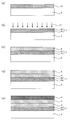
- FIG. 1 is a schematic cross-sectional view showing an example of the solar cell substrate of the present invention.
- a solar cell substrate 1 includes a transparent substrate 2 and a transparent electrode layer 3 formed on the transparent substrate 2 and containing a conductive metal oxide.
- the transparent electrode layer 3 is formed on the transparent substrate 2 and includes an amorphous film 3a containing a conductive metal oxide, and a crystal film 3b formed on the amorphous film 3a and containing a conductive metal oxide. And have.
- the amorphous film 3a and the crystal film 3b contain the same conductive metal oxide, and the crystal film 3b is obtained by crystallizing the surface of the amorphous film 3a.
- a crystalline film has a lower resistance than an amorphous film, that is, has a high conductivity.
- the crystal film has better acid resistance than the amorphous film.
- the work function is different between the amorphous film and the crystal film.
- the transparent electrode layer since the transparent electrode layer has a crystal film having a resistance lower than that of the amorphous film, the conductivity of the transparent electrode layer itself can be increased. Further, since the transparent electrode layer has an amorphous film having excellent flexibility, it is possible to maintain the flexibility of the transparent electrode layer itself. Therefore, in the present invention, a transparent electrode layer having both low resistance and flexibility can be obtained.
- the transparent electrode layer when the transparent substrate is a flexible film substrate, the transparent electrode layer has an amorphous film and is excellent in flexibility. It is possible to obtain a high-performance flexible solar cell by using
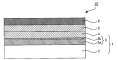
- FIG. 2 is a schematic cross-sectional view showing an example of an organic thin-film solar cell having the solar cell substrate of the present invention.
- An organic thin film solar cell 10 shown in FIG. 2 includes a solar cell substrate 1, a buffer layer 4 formed on the transparent electrode layer 3, a photoelectric conversion layer 5 formed on the buffer layer 4, and a photoelectric conversion layer 5.
- the transparent electrode layer has an amorphous film and a crystal film, and the crystal film having excellent acid resistance is formed on the buffer layer side. Therefore, in the organic thin film solar cell as shown in FIG. 2, when the buffer layer contains an acidic material, the buffer layer is not in direct contact with the amorphous film, and the Since the film is protected, damage to the transparent electrode layer due to the influence of the acid contained in the buffer layer can be reduced. Thereby, it can suppress that a transparent electrode layer melt
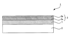
- FIG. 3 is a schematic cross-sectional view showing another example of an organic thin film solar cell having the solar cell substrate of the present invention.
- the organic thin film solar cell 20 shown in FIG. 3 has a solar cell substrate 1, an organic layer 15 formed on the transparent electrode layer 3, and a counter electrode layer 6 formed on the organic layer 15. .
- the work function is different between the amorphous film and the crystal film of the transparent electrode layer, in the organic thin film solar cell as shown in FIG. 3, the work function is set at the interface between the transparent electrode layer and the organic layer. It is possible to adjust. For example, the difference between the work function of the crystalline film and the work function of the organic layer in direct contact with the transparent electrode layer is greater than the difference between the work function of the amorphous film and the work function of the organic layer in direct contact with the transparent electrode layer. When it is small, the charge mobility from the organic layer to the transparent electrode layer can be improved.
- the transparent electrode layer in the present invention is formed on a transparent substrate, formed on the transparent substrate, and formed on the amorphous film containing the conductive metal oxide and the amorphous film. And a crystalline film containing the same conductive metal oxide as the conductive metal oxide contained in the amorphous film.
- the amorphous film and the crystalline film contain the same conductive metal oxide, and the crystalline film is obtained by crystallizing the surface of the amorphous film. Even if the elemental composition of the conductive metal oxide changes during the process of crystallizing the amorphous film to obtain the crystal film, the conductive metal oxide contained in the amorphous film and the crystal film contain it.
- the conductive metal oxides to be used are the same.
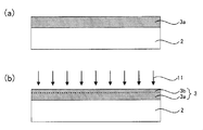
- the transparent electrode layer has an amorphous film and a crystal film by etching the transparent electrode layer.
- the transparent electrode layer is amorphous by comparing the etching rates of the transparent electrode layer, the electrode layer whose whole layer is an amorphous film, and the electrode layer whose whole layer is a crystalline film. It can be confirmed that the film has a film and a crystal film.
- the amount of decrease in the film thickness of the crystal film is smaller than the amount of decrease in the film thickness of the amorphous film.
- the amount of film thickness reduction is measured with a step gauge. The amount of decrease in the thickness of the transparent electrode layer ranges between the amount of decrease in the thickness of the electrode layer whose entire layer is an amorphous film and the amount of decrease in the thickness of the electrode layer whose entire layer is a crystalline film. If it is within the range, the transparent electrode layer is determined to have an amorphous film and a crystalline film.
- the transparent electrode layer is usually an electrode for extracting holes generated in the photoelectric conversion layer (hole extraction electrode).
- the transparent electrode layer has transparency, and the transparent electrode layer side is the light receiving surface.
- Conductive metal oxides used for amorphous films and crystal films are conductive and transparent, have an amorphous structure and a crystal structure, and can have low resistance and high acid resistance due to crystallization. There is no particular limitation as long as it can be crystallized by annealing treatment.
- a conductive metal oxide indium tin oxide (ITO) is preferably used. This is because ITO has conductivity and transparency and has a high work function. Further, when ITO is used, only the layer surface can be crystallized by laser annealing.
- the crystal film preferably has a work function comparable to that when the conductive metal oxide has a crystal structure. That is, it is preferable that the surface of the transparent electrode layer is crystallized until it has a work function comparable to that when the conductive metal oxide has a crystal structure.
- the work function of the crystal film varies depending on the type of conductive metal oxide. For example, when the conductive metal oxide is ITO, the crystal film preferably has a work function of about 4.6 eV to 4.9 eV.
- the work function of the crystal film can be obtained by measuring the work function of the surface of the transparent electrode layer on which the crystal film is formed.
- the sheet resistance of the transparent electrode layer is preferably 100 ⁇ / ⁇ or less, more preferably 50 ⁇ / ⁇ or less, and particularly preferably 20 ⁇ / ⁇ or less. If the sheet resistance of the transparent electrode layer having an amorphous film and a crystal film is in the above range, sufficient conductivity can be obtained. In addition, the said sheet resistance is measured based on JIS R1637 (Resistance test method of fine ceramics thin film: Measurement method by 4 probe method) using a surface resistance meter (Loresta MCP: Four-terminal probe) manufactured by Mitsubishi Chemical Corporation. It is the value.
- the film thickness of the transparent electrode layer is preferably in the range of 0.1 nm to 500 nm, and more preferably in the range of 10 nm to 300 nm. If the film thickness is smaller than the above range, the sheet resistance of the transparent electrode layer may become too large, and the generated charge may not be sufficiently transmitted to the external circuit. This is because the rate may decrease and the photoelectric conversion efficiency may decrease.
- the thickness of the crystal film in the transparent electrode layer may be such that the transparent electrode layer has flexibility. If the crystal film is thick, the flexibility of the transparent electrode layer may be impaired. Therefore, in order to increase the flexibility of the transparent electrode layer, the thickness of the crystal film is preferably relatively thin. Further, when the solar cell substrate of the present invention is an organic thin film solar cell substrate, the thickness of the crystal film in the transparent electrode layer may be any thickness that has acid resistance. If the crystal film is thin, desired acid resistance may not be obtained. On the other hand, if the crystal film is thick, the flexibility of the transparent electrode layer is impaired. If the thickness of the crystal film is equal to or greater than a certain level, sufficient acid resistance can be obtained. Therefore, in order to increase the flexibility of the transparent electrode layer, the thickness of the crystal film is preferably relatively thin among the acid-resistant thicknesses.
- the total light transmittance of the transparent electrode layer is preferably 85% or more, more preferably 90% or more, and particularly preferably 92% or more. This is because when the total light transmittance of the transparent electrode layer is within the above range, light can be sufficiently transmitted through the transparent electrode layer, and light can be efficiently absorbed by the photoelectric conversion layer.
- the total light transmittance is a value measured using an SM color computer (model number: SM-C) manufactured by Suga Test Instruments Co., Ltd. in the visible light region.
- the transparent electrode layer may be formed on the entire surface of the transparent substrate, or may be formed in a pattern.
- the crystal film 3b may be formed on the entire surface of the amorphous film 3a as illustrated in FIG. 1, and is formed in a pattern on the amorphous film 3a as illustrated in FIG. May be.
- the crystal film is formed in a pattern on the amorphous film, for example, an organic thin film solar cell 10 as shown in FIG. 5 is obtained. Even in such a case, the device performance can be improved.
- Transparent substrate The transparent substrate used in the present invention supports the transparent electrode layer.
- the transparent substrate is not particularly limited.
- inflexible transparent rigid material such as quartz glass, Pyrex (registered trademark), synthetic quartz plate, or flexible resin such as transparent resin film and optical resin plate.
- the transparent flexible material which has property can be mentioned.
- a transparent substrate is flexible materials, such as a transparent resin film. This is because the transparent resin film is excellent in workability, is useful in realizing a reduction in manufacturing cost, weight reduction, and a solar cell that is difficult to break, and expands the applicability to various applications such as application to curved surfaces.
- a barrier layer is formed on the transparent substrate surface.
- an inorganic thin film such as silicon oxide (SiO 2 ), silicon oxynitride (SiON), or silicon nitride (SiN) is generally formed by a vacuum film formation method or the like.
- the barrier layer can be the same as that described in JP-A-2007-73717.
- a heat insulating layer 7 may be formed between the transparent substrate 2 and the transparent electrode layer 3 as illustrated in FIG. This is because when the surface of an amorphous film is crystallized by laser annealing to form a crystal film, the heat insulating layer can protect the transparent substrate from heat.
- a heat insulating layer is preferably formed. Since the heat absorption amount of the film substrate due to laser annealing is reduced by the heat insulating layer, it is possible to prevent the transparent electrode layer from being broken or broken due to the thermal expansion of the film substrate.
- the material for forming the heat insulating layer is not particularly limited as long as it has a low thermal conductivity and heat resistance.
- Preferred examples include silicon oxide (SiO 2 ) and silicon oxynitride (SiON). Etc. This is because a heat insulating layer using these materials also functions as a barrier layer.
- the thickness of the heat insulating layer is not particularly limited as long as it can protect the transparent substrate from the heat during laser annealing, and can be set to about 0.1 ⁇ m to 2 ⁇ m, for example.
- Examples of the method for forming the heat insulating layer include a vapor deposition method such as a sputtering method and a coating method such as a spin coating method.
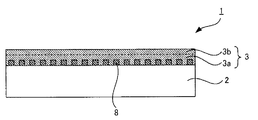
- a patterned auxiliary electrode 8 may be formed between the transparent substrate 2 and the transparent electrode layer 3. Even when the sheet resistance of the transparent electrode layer is relatively high, the resistance of the entire laminate of the transparent electrode layer and the auxiliary electrode can be reduced by sufficiently reducing the sheet resistance of the auxiliary electrode. Therefore, the generated power can be collected efficiently.
- the auxiliary electrode used in the present invention is formed in a pattern on a transparent substrate.
- the auxiliary electrode usually has a lower resistance value than the transparent electrode layer.
- a metal is usually used as a material for forming the auxiliary electrode.
- the metal used for the auxiliary electrode include aluminum (Al), gold (Au), silver (Ag), cobalt (Co), nickel (Ni), platinum (Pt), copper (Cu), and titanium (Ti).
- conductive metals such as iron (Fe), stainless steel, aluminum alloy, copper alloy, titanium alloy, iron-nickel alloy and nickel-chromium alloy (Ni-Cr).
- conductive metals described above those having a relatively low electrical resistance value are preferred. Examples of such a conductive metal include Al, Au, Ag, and Cu.
- the auxiliary electrode may be a single layer made of the conductive metal as described above, and a conductive metal layer and a contact layer are appropriately laminated in order to improve adhesion to the transparent substrate or the transparent electrode layer. It may be what you did.
- the material for forming the contact layer include nickel (Ni), chromium (Cr), nickel chromium (Ni—Cr), titanium (Ti), and tantalum (Ta).
- the contact layer is laminated on the conductive metal layer in order to obtain adhesion between the desired auxiliary electrode and the transparent substrate or transparent electrode layer, and may be laminated only on one side of the conductive metal layer. You may laminate
- the transparent electrode layer is a hole extraction electrode
- the metal used for the auxiliary electrode has a high work function. Specifically, Al is preferably used.
- the shape of the auxiliary electrode is not particularly limited as long as it is a pattern, and is appropriately selected depending on desired conductivity, permeability, strength, and the like.
- the auxiliary electrode may have a mesh-shaped mesh portion and a frame portion arranged around the mesh portion, or may be formed of a mesh-shaped mesh portion.
- the mesh portion and the frame portion may be arranged, for example, when the auxiliary electrode is rectangular, the frame portion may be arranged so as to surround four sides of the mesh portion. Further, it may be arranged so as to surround three sides of the mesh part, may be arranged so as to surround two sides of the mesh part, or may be arranged on one side of the mesh part. Especially, it is preferable that the frame part is arrange
- the shape of the mesh portion is not particularly limited as long as it is a mesh shape, and is appropriately selected depending on desired conductivity, permeability, strength, and the like.
- a polygon such as a triangle, a quadrangle, and a hexagon, a circular lattice, and the like can be given.
- a polygon or circular “lattice shape” refers to a shape in which polygons or circles are periodically arranged.
- polygonal or circular lattice shape for example, polygonal openings may be arranged in a straight line or zigzag.
- the shape of the mesh portion is preferably a hexagonal lattice shape or a parallelogram lattice shape. This is because the current flowing through the mesh portion can be prevented from being concentrated locally.
- the hexagonal openings are arranged in a zigzag (so-called honeycomb shape).
- the acute angle of the parallelogram is preferably within the range of 40 ° to 80 °, more preferably within the range of 50 ° to 70 °, and even more preferably 55 ° to 65 °. Within the range of °.
- the opening of the mesh part of the auxiliary electrode is relatively large.
- the ratio of the openings in the mesh portion of the auxiliary electrode is preferably about 50% to 98%, more preferably in the range of 70% to 98%, and still more preferably in the range of 80% to 98%. Within range.
- the pitch of the openings of the mesh portion of the auxiliary electrode and the line width of the mesh portion are appropriately selected according to the area of the entire auxiliary electrode and the like.
- the line width of the frame portion is appropriately selected according to the area of the entire auxiliary electrode.
- the thickness of the auxiliary electrode is not limited as long as it does not cause a short circuit between the transparent electrode layer and the counter electrode layer.
- the thickness of the auxiliary electrode is not limited to the thickness of the layer formed between the transparent electrode layer and the counter electrode layer. It is selected as appropriate. For example, in the case of an organic thin film solar cell, the thickness of the auxiliary electrode is appropriately selected according to the thickness of the photoelectric conversion layer, the buffer layer, and the like.
- the thickness of the auxiliary electrode is It is preferably 5 or less, more preferably 3 or less, further 2 or less, particularly preferably 1.5 or less, and most preferably 1 or less. This is because if the thickness of the auxiliary electrode is larger than the above range, a short circuit may occur between the electrodes.
- the thickness of the auxiliary electrode is preferably in the range of 100 nm to 1000 nm, more preferably in the range of 200 nm to 800 nm, further in the range of 200 nm to 500 nm, particularly in the range of 200 nm to 400 nm. It is preferable. This is because if the thickness of the auxiliary electrode is thinner than the above range, the sheet resistance of the auxiliary electrode may become too large. Moreover, it is because there exists a possibility that a short circuit may arise between electrodes when the thickness of an auxiliary electrode is thicker than the said range.
- the photoelectric conversion layer is formed on the transparent electrode layer by a method capable of adjusting the thickness mainly in accordance with the coating amount.
- the thickness of the auxiliary electrode is preferably in the range of 200 nm to 300 nm.
- the photoelectric conversion layer may be formed thicker than the desired thickness due to surface tension. If the thickness of the photoelectric conversion layer is too thick, it exceeds the electron diffusion length and the hole diffusion length, and the conversion efficiency decreases. It is preferable to adjust the thickness of the auxiliary electrode so that the photoelectric conversion layer is not formed thicker than desired due to surface tension. In particular, since it is known that the distance that holes and electrons can move in the photoelectric conversion layer is about 100 nm, the auxiliary electrode is formed so that the photoelectric conversion layer is not formed thicker than the desired thickness due to surface tension. It is preferable to adjust the thickness.
- the photoelectric conversion layer is formed by, for example, a spin coating method
- a uniform film is formed by centrifugal force, so that the edge of the auxiliary electrode can be covered even if the auxiliary electrode is relatively thick.
- the thickness can be adjusted by the number of rotations, so that a uniform film can be obtained even if the auxiliary electrode is relatively thick. Therefore, when the photoelectric conversion layer is formed mainly by a method capable of adjusting the thickness according to the coating amount, the above range is particularly preferable.
- the sheet resistance of the auxiliary electrode may be lower than that of the transparent electrode layer.
- the sheet resistance of the auxiliary electrode is preferably 5 ⁇ / ⁇ or less, more preferably 3 ⁇ / ⁇ or less, more preferably 1 ⁇ / ⁇ or less, particularly preferably 0.5 ⁇ / ⁇ or less, and 0.1 ⁇ . Most preferably, it is less than / ⁇ . This is because if the sheet resistance of the auxiliary electrode is larger than the above range, desired power generation efficiency may not be obtained.
- the said sheet resistance is measured based on JIS R1637 (Resistance test method of fine ceramics thin film: Measurement method by 4 probe method) using a surface resistance meter (Loresta MCP: Four-terminal probe) manufactured by Mitsubishi Chemical Corporation. It is the value.
- the method for forming the auxiliary electrode is not particularly limited, and examples thereof include a method in which a metal thin film is formed on the entire surface and then patterned in a mesh shape, and a method in which a mesh-like conductor is directly formed. These methods are appropriately selected depending on the auxiliary electrode forming material, configuration, and the like.
- the method for forming the metal thin film is preferably a vacuum film forming method such as a vacuum deposition method, a sputtering method, or an ion plating method. That is, the auxiliary electrode is preferably a metal thin film formed by a vacuum film forming method.
- the metal species formed by the vacuum film formation method has less inclusions than the plating film and can reduce the specific resistance, and can also reduce the specific resistance as compared with those formed using Ag paste or the like.
- a vacuum film formation method is also suitable as a method for forming a metal thin film having a thickness of 1 ⁇ m or less, preferably 500 nm or less, with a precise thickness and a uniform thickness.
- the method for patterning the metal thin film is not particularly limited as long as it can be accurately formed into a desired pattern, and examples thereof include a photoetching method.
- the solar cell substrate of the present invention is used for solar cells in general, and can be used for organic thin film solar cells, dye-sensitized solar cells, compound semiconductor solar cells, silicon solar cells, and the like. .
- substrate for solar cells of this invention is used for an organic thin film solar cell, a dye-sensitized solar cell, a compound semiconductor solar cell, and an amorphous silicon solar cell. Since these solar cells have relatively high resistance to bending, they are suitable as flexible solar cells and are suitable for the solar cell substrate of the present invention.
- the solar cell substrate of the present invention is preferably an organic thin film solar cell substrate.
- the resistance of the transparent electrode layer can be reduced, damage to the transparent electrode layer due to acid can be suppressed, and electrical characteristics can be improved.
- the solar cell of the present invention includes the above-described solar cell substrate.
- the solar cell substrate is provided, a transparent electrode layer having both low resistance and flexibility can be obtained. Further, when the transparent substrate is a flexible film substrate, the transparent electrode layer has an amorphous film and is excellent in flexibility, so that a high-performance flexible solar cell can be obtained. is there.
- the type of the solar cell of the present invention is not particularly limited, and examples thereof include an organic thin film solar cell, a dye-sensitized solar cell, a compound semiconductor solar cell, and a silicon solar cell.
- compound semiconductor solar cells include III-V compound semiconductor solar cells such as gallium arsenide (GaAs) and indium phosphorus (InP), and II-VI compound semiconductor solar cells such as cadmium tellurium (CdTe).
- III-V compound semiconductor solar cells such as gallium arsenide (GaAs) and indium phosphorus (InP)
- II-VI compound semiconductor solar cells such as cadmium tellurium (CdTe).
- Examples include batteries, I-III-VI group compound semiconductor solar cells such as CIS (CuInSe 2 ) and CIGS (Cu (In, Ga) Se 2 ).
- the silicon-based solar cell examples include a single crystal silicon solar cell, a polycrystalline silicon solar cell, and a single junction type or tandem structure type amorphous silicon solar cell.
- a thin film polycrystalline silicon solar cell, a thin film microcrystalline silicon solar cell, a hybrid solar cell of a thin film crystalline silicon solar cell and an amorphous silicon solar cell can also be mentioned.
- the solar cell of the present invention is preferably an organic thin film solar cell, a dye-sensitized solar cell, a compound semiconductor solar cell, or an amorphous silicon solar cell. This is because these solar cells have a relatively high resistance to bending, and thus are suitable as flexible solar cells and useful.
- An organic thin film solar cell is particularly suitable. This is because the acid resistance can be improved in the present invention as described above.
- the organic thin film solar cell the dye-sensitized solar cell, the compound semiconductor solar cell, and the silicon solar cell will be described separately.
- Organic thin-film solar cell of the present invention comprises the above-described solar cell substrate, a solar cell substrate, a photoelectric conversion layer formed on the transparent electrode layer of the solar cell substrate, A counter electrode layer formed on the photoelectric conversion layer.
- the solar cell substrate has been described in detail in the section “A. Solar Cell Substrate” above, and will not be described here.
- the organic thin film solar cell will be described in detail in the section “C. Organic thin film solar cell” described later, and the description thereof will be omitted here.
- the dye-sensitized solar cell of the present invention includes the above-described solar cell substrate, and is formed, for example, on the solar cell substrate and the transparent electrode layer of the solar cell substrate.
- the solar cell substrate has been described in detail in the section “A. Solar Cell Substrate” above, and will not be described here. Hereinafter, other configurations in the dye-sensitized solar cell will be described.
- Porous layer contains oxide semiconductor fine particles carrying a dye sensitizer.
- oxide semiconductor fine particles carrying a dye sensitizer carrying a dye sensitizer.
- the oxide semiconductor fine particles are not particularly limited as long as they are made of an oxide having semiconductor characteristics.
- the oxide constituting the oxide semiconductor fine particles include TiO 2 , ZnO, SnO 2 , ITO, ZrO 2 , MgO, Al 2 O 3 , CeO 2 , Bi 2 O 3 , Mn 3 O 4 , and Y 2 O. 3 , WO 3 , Ta 2 O 5 , Nb 2 O 5 , La 2 O 3 and the like.
- These oxide semiconductor fine particles are suitable for forming a porous porous layer, and are preferably used because energy conversion efficiency can be improved and cost can be reduced.
- the oxide semiconductor fine particles may all be made of the same oxide, or two or more kinds of oxide semiconductor fine particles may be used.
- One kind of oxide semiconductor fine particles may be a core fine particle, and another oxide semiconductor may have a core-shell structure including a core fine particle to form a shell.
- oxide semiconductor fine particles made of TiO 2 it is most preferable to use oxide semiconductor fine particles made of TiO 2 . This is because TiO 2 is particularly excellent in semiconductor characteristics.
- the average particle diameter of the oxide semiconductor fine particles is not particularly limited as long as the specific surface area of the porous layer is within a desired range, but is preferably within a range of 1 nm to 10 ⁇ m, and particularly 10 nm to 1000 nm. It is preferable to be within the range. If the average particle size is smaller than the above range, the respective oxide semiconductor fine particles may aggregate to form secondary particles. If the average particle size is larger than the above range, the porous layer becomes thicker. This is because the porosity of the porous layer, that is, the specific surface area may be reduced. Here, when the specific surface area of the porous layer becomes small, for example, it may be difficult to carry a dye sensitizer sufficient for photoelectric conversion on the porous layer. Note that the average particle size of the oxide semiconductor fine particles means a primary particle size.
- oxide semiconductor fine particles those having the same average particle diameter may be used, or a plurality of oxide semiconductor fine particles having different average particle diameters may be used.
- oxide semiconductor fine particles having different average particle diameters By using together oxide semiconductor fine particles having different average particle diameters, the light scattering effect in the porous layer can be enhanced, and there is an advantage that the dye-sensitized solar cell can be made more excellent in power generation efficiency.
- the combination of the different average particle diameters is, for example, oxide semiconductor fine particles having an average particle diameter in the range of 10 nm to 50 nm and an average particle diameter of 50 nm.
- oxide semiconductor fine particles in the range of ⁇ 800 nm can be exemplified.
- the dye sensitizer is not particularly limited as long as it can absorb light and generate an electromotive force.
- a dye sensitizer include organic dyes and metal complex dyes.
- the organic dye include acridine, azo, indigo, quinone, coumarin, merocyanine, and phenylxanthene dyes. Among these organic dyes, it is preferable to use a coumarin dye.
- the metal complex dye it is preferable to use a ruthenium dye, and it is particularly preferable to use a ruthenium bipyridine dye and a ruthenium terpyridine dye which are ruthenium complexes. This is because such a ruthenium complex has a wide wavelength range of light to be absorbed, so that the wavelength range of light that can be photoelectrically converted can be greatly expanded.
- the porous layer may contain an optional component in addition to the oxide semiconductor fine particles.
- binder resin can be mentioned, for example. It is because a porous layer can be made into a thing with low brittleness by containing binder resin in a porous layer.
- the binder resin is not particularly limited as long as the brittleness of the porous layer can be set to a desired level. However, since the porous layer is formed in contact with the electrolyte layer as described later, it is necessary to use a binder resin having resistance to the electrolyte layer.
- a binder resin include polyvinyl pyrrolidone, ethyl cellulose, caprolactan, and the like. There may be only one type of binder resin, or two or more types.
- the thickness of the porous layer is appropriately selected according to the use of the dye-sensitized solar cell and is not particularly limited.
- the thickness of the porous layer is preferably in the range of 1 ⁇ m to 100 ⁇ m, and particularly preferably in the range of 3 ⁇ m to 30 ⁇ m. This is because if the thickness of the porous layer is larger than the above range, the porous layer itself tends to cause cohesive failure, which tends to cause membrane resistance.
- the thickness of the porous layer is thinner than the above range, it becomes difficult to form a porous layer having a uniform thickness, or the amount of the dye sensitizer carried is reduced, so that the sunlight is sufficiently absorbed. This is because there is a possibility that performance may be deteriorated because it is not possible.
- the porous layer may be formed on one surface or a pattern on the solar cell substrate.
- the method for forming the porous layer can be the same as the general method for forming a porous layer in a dye-sensitized solar cell.
- Electrolyte layer The electrolyte layer is formed so as to be in contact with the porous layer between the transparent electrode layer and the counter electrode layer of the solar cell substrate.
- the electrolyte layer may be in any form of gel, solid or liquid.
- the electrolyte layer may or may not contain a redox pair.
- the redox couple is not particularly limited as long as it is generally used in an electrolyte layer of a dye-sensitized solar cell. A combination, a combination of bromine and bromide is preferred.
- Examples of the combination of iodine and iodide are used as the redox pair may be, for example, LiI, NaI, KI, and metal iodide such as CaI 2, a combination of I 2.
- Examples of the combination of bromine and bromide include a combination of a metal bromide such as LiBr, NaBr, KBr, CaBr 2 and Br 2 .
- the electrolyte layer When the electrolyte layer is in a liquid state, for example, acetonitrile, methoxyacetonitrile, propylene carbonate or the like is used as a solvent, and a redox couple containing the same or an ionic liquid having an imidazolium salt as a cation is used as the solvent. Can do.
- the electrolyte layer when it is in a gel form, it may be either a physical gel or a chemical gel.
- the physical gel is gelled near room temperature due to physical interaction
- the chemical gel is a gel formed by chemical bonding by a crosslinking reaction or the like.
- a solid electrolyte layer what consists of CuI, a polypyrrole, polythiophene etc. can be mentioned, for example.
- a catalyst layer may be formed between the counter electrode layer, the porous layer, and the electrolyte layer as necessary.
- the catalyst layer By forming the catalyst layer on the counter electrode layer, the dye-sensitized solar cell can be made more excellent in power generation efficiency.
- examples of such a catalyst layer include an embodiment in which Pt is deposited on the counter electrode layer, polyethylene dioxythiophene (PEDOT), polystyrene sulfonic acid (PSS), polyaniline (PA), paratoluene sulfonic acid (PTS) and Although the aspect which forms a catalyst layer from these mixtures can be mentioned, it is not this limitation.
- a sealant layer may be formed for sealing.
- the sealing agent used for the sealing agent layer is not particularly limited as long as it has durability to the electrolyte layer.
- various thermoplastic resins and thermoplastic elastomers that can be heat sealed, low density Random or block co-polymerization of ⁇ -olefins such as polyethylene, high-density polyethylene, polypropylene, poly-1-butene, poly-4-methyl-1-pentene, or ethylene, propylene, 1-butene, 4-methyl-1-pentene
- Polyolefin resins such as copolymers; ethylene-vinyl compound copolymer resins such as ethylene-vinyl acetate copolymer, ethylene-vinyl alcohol copolymer, ethylene-vinyl chloride copolymer; polystyrene, acrylonitrile-styrene copolymer, Styrene such as ABS, ⁇ -methyl
- the thickness of the sealing agent layer is preferably in the range of 1 ⁇ m to 100 ⁇ m, and more preferably in the range of 1 ⁇ m to 50 ⁇ m.
- the counter electrode layer can be the same as the counter electrode layer in the organic thin film solar cell described later.
- the counter electrode layer may be formed on the counter substrate.
- the counter substrate can be the same as the above-described transparent substrate of the solar cell substrate, and thus description thereof is omitted here.
- the compound semiconductor solar cell of the present invention includes the above-described solar cell substrate, and is formed on the solar cell substrate and the transparent electrode layer of the solar cell substrate. It has a semiconductor layer to be contained and a counter electrode layer disposed on the semiconductor layer.
- the solar cell substrate has been described in detail in the section “A. Solar Cell Substrate” above, and will not be described here. Hereinafter, other configurations of the compound semiconductor solar cell will be described.
- a semiconductor layer is a layer containing a compound semiconductor.
- compound semiconductors include III-V group compound semiconductors such as gallium arsenide (GaAs) and indium phosphorus (InP), II-VI group compound semiconductors such as cadmium tellurium (CdTe), CIS (CuInSe 2 ), and CIGS (Cu Examples include I-III-VI group compound semiconductors such as (In, Ga) Se 2 ).
- Counter electrode layer The counter electrode layer can be the same as the counter electrode layer in the organic thin film solar cell described later.
- Silicon-based solar cell The silicon-based solar cell of the present invention includes the above-described solar cell substrate, and is a semiconductor that is formed on the solar cell substrate and the transparent electrode layer of the solar cell substrate and contains silicon. And a counter electrode layer disposed on the semiconductor layer.
- the solar cell substrate has been described in detail in the section “A. Solar Cell Substrate” above, and will not be described here. Hereinafter, other configurations of the silicon-based solar cell will be described.
- the semiconductor layer is a layer containing silicon.
- silicon include single crystal silicon, polycrystalline silicon, and amorphous silicon.
- the semiconductor layer may be a stack of a layer containing thin film polycrystalline silicon, thin film microcrystalline silicon, or thin film crystal silicon, and a layer containing amorphous silicon. In this case, a hybrid solar cell can be obtained.
- Counter electrode layer The counter electrode layer can be the same as the counter electrode layer in the organic thin film solar cell described later.
- the organic thin film solar cell of the present invention includes a transparent substrate, a transparent electrode layer formed on the transparent substrate, a buffer layer formed on the transparent electrode layer, and a photoelectric conversion layer formed on the buffer layer. And a counter electrode layer formed on the photoelectric conversion layer, wherein the transparent electrode layer is an amorphous material formed on the transparent substrate and containing a conductive metal oxide. And a crystalline film formed on the amorphous film and containing the same conductive metal oxide as the conductive metal oxide contained in the amorphous film. It is. That is, the organic thin-film solar cell of the present invention includes the above-described solar cell substrate, and a buffer layer is formed on the transparent electrode layer.
- FIG. 2 is a schematic cross-sectional view showing an example of the organic thin film solar cell of the present invention.
- the organic thin-film solar cell 10 includes a solar cell substrate 1, a buffer layer 4 formed on the transparent electrode layer 3 of the solar cell substrate 1, and a photoelectric film formed on the buffer layer 4. It has a conversion layer 5 and a counter electrode layer 6 formed on the photoelectric conversion layer 5.
- the solar cell substrate 1 has a transparent substrate 2 and a transparent electrode layer 3 formed on the transparent substrate 2 and containing a conductive metal oxide.
- the transparent electrode layer 3 is formed on the transparent substrate 2 and is formed on the amorphous film 3a containing the conductive metal oxide and in contact with the buffer layer 4 on the amorphous film 3a. And a crystal film 3b containing.
- the amorphous film 3a and the crystal film 3b contain the same conductive metal oxide, and the crystal film 3b is obtained by crystallizing the surface of the amorphous film 3a.
- the solar cell substrate is provided, a transparent electrode layer having both low resistance and flexibility can be obtained. Further, when the transparent substrate is a flexible film substrate, the transparent electrode layer has an amorphous film and is excellent in flexibility, so that a high-performance flexible organic thin film solar cell can be obtained. Is possible.
- the solar cell substrate since the solar cell substrate is included, when the buffer layer contains a material exhibiting acidity, it is due to the influence of the acid contained in the buffer layer when the buffer layer is formed and when the solar cell is used. It is possible to reduce damage to the transparent electrode layer. Thereby, it is possible to suppress the deterioration of the electrical characteristics of the transparent electrode layer and to improve the reliability of the organic thin film solar cell.
- the transparent substrate, the transparent electrode layer, the heat insulating layer, and the auxiliary electrode have been described in detail in the above section “A. Solar Cell Substrate”, and thus description thereof is omitted here.
- the other structure in the organic thin-film solar cell of this invention is demonstrated.
- Buffer layer The buffer layer in the present invention is formed directly on the transparent electrode layer, and is a layer provided so that the charge can be easily taken out from the photoelectric conversion layer to the transparent electrode layer. Since the transparent electrode layer is usually a hole extraction electrode, the buffer layer is preferably a layer provided so that holes can be easily extracted from the photoelectric conversion layer to the transparent electrode layer. Since the hole extraction efficiency from the photoelectric conversion layer to the transparent electrode layer is increased by the buffer layer, the photoelectric conversion efficiency can be improved.
- the material used for the buffer layer is not particularly limited as long as it is a material that stabilizes the extraction of holes from the photoelectric conversion layer to the transparent electrode layer.
- conductive organic compounds such as doped polyaniline, polyphenylene vinylene, polythiophene, polypyrrole, polyparaphenylene, polyacetylene, triphenyldiamine (TPD), or electron donation such as tetrathiofulvalene, tetramethylphenylenediamine, etc.
- An organic material that forms a charge transfer complex composed of an organic compound and an electron-accepting compound such as tetracyanoquinodimethane and tetracyanoethylene.
- PEDOT / PSS polyethylene dioxythiophene / polystyrene sulfonic acid
- the material used for a buffer layer is what shows acidity. Specifically, a material having a pH of less than 7 when used as a coating solution is preferable. As described above, when the buffer layer contains a material exhibiting acidity, the damage of the transparent electrode layer due to the influence of the acid contained in the buffer layer can be reduced, so the configuration of the present invention is useful. Examples of the material showing acidity include PEDOT / PSS and doped polyaniline, and PEDOT / PSS is particularly preferably used. That is, the buffer layer preferably contains PEDOT / PSS. PEDOT / PSS is a material that exhibits acidity in the coating liquid for forming the buffer layer, and also exhibits acidity in the buffer layer when the buffer layer absorbs moisture. Therefore, it is useful that the transparent electrode layer has a crystal film on the buffer layer side as in the configuration of the present invention.
- the thickness of the buffer layer is preferably in the range of 10 nm to 200 nm.
- the photoelectric conversion layer used in the present invention is formed between the transparent electrode layer and the counter electrode layer.
- the “photoelectric conversion layer” refers to a member that contributes to charge separation of the organic thin film solar cell and has a function of transporting generated electrons and holes toward electrodes in opposite directions.
- the photoelectric conversion layer may be a single layer having both an electron-accepting function and an electron-donating function (first aspect), or an electron-accepting layer having an electron-accepting function and an electron-donating function.
- a layer in which an electron donating layer having n is laminated may be used (second embodiment).
- the 1st aspect of the photoelectric converting layer in this invention is a single layer which has both an electron-accepting function and an electron-donating function, and contains an electron-donating material and an electron-accepting material It is.
- this photoelectric conversion layer since charge separation occurs using a pn junction formed in the photoelectric conversion layer, it functions as a photoelectric conversion layer alone.
- the electron donating material is not particularly limited as long as it has a function as an electron donor, but it is preferable that the material can be formed by a wet coating method.
- a polymer material is preferred.
- a conductive polymer is a so-called ⁇ -conjugated polymer, which is composed of a ⁇ -conjugated system in which double bonds or triple bonds containing carbon-carbon or hetero atoms are alternately linked to single bonds, and exhibits semiconducting properties. It is. In the conductive polymer material, ⁇ conjugation is developed in the polymer main chain, so that charge transport in the main chain direction is basically advantageous.
- the electron transfer mechanism of the conductive polymer is mainly hopping conduction between molecules by ⁇ stacking, it is advantageous not only for the main chain direction of the polymer but also for the charge transport in the film thickness direction of the photoelectric conversion layer. is there.
- the conductive polymer material can be easily formed by a wet coating method using a coating solution in which the conductive polymer material is dissolved or dispersed in a solvent, a large-area organic thin film solar cell Can be manufactured at low cost without requiring expensive equipment.
- Examples of the electron-donating conductive polymer material include polyphenylene, polyphenylene vinylene, polysilane, polythiophene, polycarbazole, polyvinyl carbazole, porphyrin, polyacetylene, polypyrrole, polyaniline, polyfluorene, polyvinyl pyrene, polyvinyl anthracene, and derivatives thereof. And copolymers thereof, or phthalocyanine-containing polymers, carbazole-containing polymers, organometallic polymers, and the like.
- thiophene-fluorene copolymer polyalkylthiophene, phenylene ethynylene-phenylene vinylene copolymer, phenylene ethynylene-thiophene copolymer, phenylene ethynylene-fluorene copolymer, fluorene-phenylene vinylene copolymer
- a thiophene-phenylene vinylene copolymer is preferably used. This is because the energy level difference is appropriate for many electron-accepting materials.
- a phenylene ethynylene-phenylene vinylene copolymer Poly [1,4-phenyleneethynylene-1,4- (2,5-dioctadodecyloxyphenylene) -1,4-phenyleneethene-1,2-diyl-1,4- ( 2,5-dioctadodecyloxyphenylene) ethene-1,2-diyl]
- the electron-accepting material is not particularly limited as long as it has a function as an electron acceptor, but it is preferable that it can be formed into a film by a wet coating method.
- a conductive polymer material is preferable. This is because the conductive polymer material has the advantages as described above.
- Examples of the electron-accepting conductive polymer material include polyphenylene vinylene, polyfluorene, and derivatives thereof, and copolymers thereof, or carbon nanotubes, fullerene derivatives, CN group or CF 3 group-containing polymers, and the like. And —CF 3 substituted polymer.
- polyphenylene vinylene derivative examples include CN-PPV (Poly [2-Methoxy-5- (2′-ethylhexyloxy) -1,4- (1-cyanovinylene) phenylene]), MEH-CN-PPV (Poly [2 -Methoxy-5- (2′-ethylhexyloxy) -1,4- (1-cyanovinylene) phenylene]) and the like.
- an electron accepting material doped with an electron donating compound, an electron donating material doped with an electron accepting compound, or the like can be used.
- a conductive polymer material doped with an electron donating compound or an electron accepting compound is preferably used.
- Conductive polymer materials are basically advantageous in charge transport in the direction of the main chain because of the development of ⁇ conjugation in the polymer main chain, and are doped with electron-donating compounds and electron-accepting compounds. This is because electric charges are generated in the ⁇ -conjugated main chain, and the electrical conductivity can be greatly increased.
- Examples of the electron-accepting conductive polymer material doped with the electron-donating compound include the above-described electron-accepting conductive polymer material.
- a Lewis base such as an alkali metal such as Li, K, Ca, or Cs or an alkaline earth metal can be used.
- the Lewis base acts as an electron donor.
- the electron-donating conductive polymer material doped with the electron-accepting compound include the above-described electron-donating conductive polymer material.
- a Lewis acid such as FeCl 3 (III), AlCl 3 , AlBr 3 , AsF 6 or a halogen compound can be used. In addition, Lewis acid acts as an electron acceptor.
- the film thickness of the photoelectric conversion layer As the film thickness of the photoelectric conversion layer, the film thickness generally employed in bulk heterojunction organic thin-film solar cells can be employed. Specifically, it can be set within the range of 0.2 nm to 3000 nm, and preferably within the range of 1 nm to 600 nm. This is because when the film thickness is thicker than the above range, the volume resistance in the photoelectric conversion layer may increase. On the other hand, if the film thickness is thinner than the above range, light may not be sufficiently absorbed.
- the mixing ratio of the electron-donating material and the electron-accepting material is appropriately adjusted to an optimal mixing ratio depending on the type of material used.
- the method for forming the photoelectric conversion layer is not particularly limited as long as it can be uniformly formed in a predetermined film thickness, but a wet coating method is preferably used. This is because if the wet coating method is used, the photoelectric conversion layer can be formed in the air, and the cost can be reduced and the area can be easily increased.
- the method for applying the photoelectric conversion layer coating liquid is not particularly limited as long as it can uniformly apply the photoelectric conversion layer coating liquid.
- a die coating method, a spin coating method, a dip coating, and the like examples thereof include a coating method, a roll coating method, a bead coating method, a spray coating method, a bar coating method, a gravure coating method, an ink jet method, a screen printing method, and an offset printing method.
- coating method of the coating liquid for photoelectric conversion layers is a method which can adjust thickness mainly according to the application amount.
- Methods that can adjust the thickness mainly according to the coating amount include, for example, a die coating method, a bead coating method, a bar coating method, a gravure coating method, an ink jet method, a screen printing method, and an offset printing method. Can be mentioned.
- the printing method is suitable for increasing the area of the organic thin film solar cell.
- a drying treatment for drying the formed coating film may be performed. It is because productivity can be improved by removing the solvent etc. which are contained in the coating liquid for photoelectric conversion layers at an early stage.
- a drying method for example, a general method such as heat drying, air drying, vacuum drying, infrared heat drying, or the like can be used.
- the electron-accepting layer used in this embodiment has an electron-accepting function and contains an electron-accepting material.
- the electron-accepting material is not particularly limited as long as it has a function as an electron acceptor, but is preferably a material that can be formed into a film by a wet coating method.
- a polymer material is preferred. This is because the conductive polymer material has the advantages as described above. Specific examples include the same electron-accepting conductive polymer materials used for the photoelectric conversion layer of the first aspect.
- a film thickness generally employed in a bilayer type organic thin film solar cell can be employed. Specifically, it can be set within a range of 0.1 nm to 1500 nm, and preferably within a range of 1 nm to 300 nm. This is because if the film thickness is larger than the above range, the volume resistance in the electron-accepting layer may be increased. On the other hand, if the film thickness is thinner than the above range, light may not be sufficiently absorbed.
- the method for forming the electron-accepting layer can be the same as the method for forming the photoelectric conversion layer of the first aspect.
- the electron donating layer used in this embodiment has an electron donating function and contains an electron donating material.
- the electron donating material is not particularly limited as long as it has a function as an electron donor, but it is preferable that the material can be formed by a wet coating method.
- a polymer material is preferred. This is because the conductive polymer material has the advantages as described above. Specific examples include the same electron donating conductive polymer materials used for the photoelectric conversion layer of the first aspect.
- a film thickness generally employed in a bilayer type organic thin film solar cell can be employed. Specifically, it can be set within a range of 0.1 nm to 1500 nm, and preferably within a range of 1 nm to 300 nm. This is because if the film thickness is larger than the above range, the volume resistance in the electron donating layer may be increased. On the other hand, if the film thickness is thinner than the above range, light may not be sufficiently absorbed.
- the method for forming the electron donating layer can be the same as the method for forming the photoelectric conversion layer of the first aspect.
- the counter electrode layer used in the present invention is an electrode facing the transparent electrode layer.
- the counter electrode layer is an electrode (electron extraction electrode) for extracting electrons generated in the photoelectric conversion layer.
- the counter electrode layer since the transparent electrode layer side becomes the light receiving surface, the counter electrode layer may or may not have transparency.
- the material for forming the counter electrode layer is not particularly limited as long as it has conductivity. However, since the counter electrode layer is an electron extraction electrode, it preferably has a low work function. Specific examples of the material having a low work function include Li, In, Al, Ag, Ca, Mg, Sm, Tb, Yb, Zr, and LiF.
- the counter electrode layer may be a single layer or may be laminated using materials having different work functions. Examples of the counter electrode layer in which different materials are laminated include those in which any one of Ca, LiF, LiCa, MoO 3 or VO 5 and any one of Al or Ag are laminated.
- the thickness of the counter electrode layer is within a range of 0.1 nm to 500 nm, particularly 1 nm to 300 nm. It is preferable to be within the range.
- the film thickness is thinner than the above range, the sheet resistance of the counter electrode layer becomes too large, and the generated charge may not be sufficiently transmitted to the external circuit.
- the counter electrode layer may be formed on the entire surface of the photoelectric conversion layer, or may be formed in a pattern.
- a method for forming the counter electrode layer a general electrode forming method can be used. For example, a vacuum evaporation method or a pattern evaporation method using a metal mask can be used.
- an electron extraction layer may be formed between the photoelectric conversion layer and the counter electrode layer.
- the electron extraction layer is a layer provided so that electrons can be easily extracted from the photoelectric conversion layer to the electron extraction electrode. Thereby, since the electron extraction efficiency from the photoelectric conversion layer to the electron extraction electrode is increased, the photoelectric conversion efficiency can be improved.
- the material used for the electron extraction layer is not particularly limited as long as it is a material that stabilizes the extraction of electrons from the photoelectric conversion layer to the electron extraction electrode.
- conductive organic compounds such as doped polyaniline, polyphenylene vinylene, polythiophene, polypyrrole, polyparaphenylene, polyacetylene, triphenyldiamine (TPD), or electron donation such as tetrathiofulvalene, tetramethylphenylenediamine, etc.
- An organic material that forms a charge transfer complex composed of an organic compound and an electron-accepting compound such as tetracyanoquinodimethane and tetracyanoethylene.
- the metal dope layer with an alkali metal or alkaline-earth metal is mentioned.
- Suitable materials include bathocuproin (BCP) or bathophenantrone (Bphen) and metal doped layers such as Li, Cs, Ba, Sr.
- the organic thin film solar cell of the present invention may have constituent members to be described later as necessary in addition to the constituent members described above.
- the organic thin film solar cell of the present invention is a functional layer such as a protective sheet, a filler layer, a barrier layer, a protective hard coat layer, a strength support layer, an antifouling layer, a high light reflection layer, a light containment layer, a sealing material layer, etc. You may have.
- an adhesive layer may be formed between the functional layers depending on the layer configuration. These functional layers can be the same as those described in JP-A-2007-73717.
- the solar cell module of the present invention is characterized in that a plurality of the above-described solar cells are connected in series or in parallel.
- the connection of a plurality of solar cells is not limited as long as a desired electromotive force can be obtained, may be only in series, only in parallel, or a combination of series and parallel.
- B. Solar cell about the solar cell, description here is abbreviate
- Organic thin film solar cell module The organic thin film solar cell module of the present invention is characterized in that a plurality of the above organic thin film solar cells are connected in series or in parallel.
- the connection of the plurality of organic thin-film solar cells is not limited as long as a desired electromotive force can be obtained, may be only in series, may be only in parallel, or may be a combination of series and parallel. Since the organic thin film solar cell is described in detail in the section “C. Organic thin film solar cell”, description thereof is omitted here.
- an amorphous film containing a conductive metal oxide is formed on a transparent substrate, and then the surface of the amorphous film is crystallized by laser annealing to form a crystalline film. It has a transparent electrode layer forming step of forming and obtaining a transparent electrode layer having the amorphous film and the crystal film.
- FIG. 8A to 8 (b) are process charts showing an example of a method for manufacturing a solar cell substrate of the present invention.
- an amorphous film 3 a containing a conductive metal oxide is formed on the transparent substrate 2.
- the surface of the amorphous film 3a is crystallized by irradiating the laser 11 to form a crystal film 3b. Since the crystal film 3b is obtained by crystallizing the surface of the amorphous film 3a, the crystal film 3b has a lower resistance and superior acid resistance than the amorphous film 3a. Thereby, the transparent electrode layer 3 having the amorphous film 3a and the crystal film 3b is obtained (transparent electrode layer forming step).
- the transparent electrode layer since the surface of the amorphous film is crystallized by laser annealing to form a crystalline film having a lower resistance than the amorphous film, it is possible to obtain a transparent electrode layer with good conductivity. Moreover, since only the surface of the amorphous film is crystallized by laser annealing to form a crystal film, the transparent electrode layer has an amorphous film having excellent flexibility, and the transparent electrode layer having flexibility It is possible to obtain Therefore, in the present invention, a transparent electrode layer having both low resistance and flexibility can be formed.
- a transparent substrate with low heat resistance is used. It is possible. Therefore, a flexible film substrate can be used as the transparent substrate. As described above, in the present invention, a flexible transparent electrode layer can be obtained, and a flexible film substrate can be used as the transparent substrate. Therefore, a high-performance flexible solar cell can be manufactured. Is possible.
- the surface of the amorphous film is crystallized by laser annealing to form a crystalline film, for example, when an organic thin film solar cell 10 as shown in FIG.
- the buffer layer 4 is not directly formed. Therefore, when the buffer layer is formed using an acidic material, the amorphous film is protected by the crystal film, and it is possible to reduce the damage of the transparent electrode layer due to the influence of the acid contained in the buffer layer. is there. Thereby, it becomes possible to obtain an organic thin film solar cell with high reliability. Therefore, in the present invention, it is possible to produce an organic thin-film solar cell excellent in electrical performance by reducing the resistance of the transparent electrode layer and suppressing damage to the transparent electrode layer due to acid.
- the surface of the amorphous film is crystallized by laser annealing to form a crystalline film having a work function different from that of the amorphous film, and thus, for example, an organic thin film solar cell 20 as shown in FIG.
- Transparent electrode layer forming step In the transparent electrode layer forming step in the present invention, an amorphous film containing a conductive metal oxide is formed on a transparent substrate, and then the surface of the amorphous film is crystallized by laser annealing. This is a step of forming a crystal film and obtaining a transparent electrode layer having the amorphous film and the crystal film.
- the method for forming the amorphous film is not particularly limited as long as it is a method capable of forming a film having an amorphous structure.
- a sputtering method a vacuum evaporation method, an ion plating method, a thermal CVD method is used. And plasma CVD method.
- the sputtering method is preferable.
- an excimer laser can be used as the laser.
- the excimer laser include a KrF excimer laser (wavelength 248 nm), an ArF excimer laser (wavelength 193 nm), and the like.
- a KrF excimer laser having a wavelength of 248 nm is preferably used because of its versatility.
- the laser irradiation conditions are appropriately adjusted according to the damage to the amorphous film and the crystallinity of the irradiated portion.
- the output of the laser can be in a range of 70mJ / cm 2 ⁇ 110mJ / cm 2, the range among them of 80mJ / cm 2 ⁇ 100mJ / cm 2, particularly 85mJ / cm 2 ⁇ 95mJ / cm 2 It is preferable to be within the range.
- the atmosphere in laser annealing is usually an air atmosphere.
- the laser may be applied to the entire surface of the amorphous film, or the amorphous film may be irradiated in a pattern.
- the amorphous film is irradiated with laser in a pattern, the crystal film 3b is formed in a pattern on the amorphous film 3a as illustrated in FIG. Even in such a case, the device performance can be improved.
- the extent to which the amorphous film surface is crystallized by laser annealing is appropriately adjusted in consideration of the conductivity, flexibility, and acid resistance of the obtained transparent electrode layer.
- the surface of the amorphous film is preferably crystallized until the crystal film obtained by crystallization has a work function comparable to that when the conductive metal oxide has a crystal structure. . If the progress of crystallization is insufficient, the desired acid resistance may not be obtained. On the other hand, if crystallization proceeds excessively, the flexibility of the transparent electrode layer is impaired. When the crystallization progresses to a certain extent, the work function hardly changes. Therefore, in order to obtain high flexibility, the laser annealing may be stopped immediately after the crystal film has a work function comparable to that when the conductive metal oxide has a crystal structure. preferable.
- the surface of the amorphous film is crystallized can be confirmed by etching the film after laser annealing. Specifically, by comparing the etching rates of the film after laser annealing, the film whose entire layer is an amorphous film, and the film whose entire layer is a crystalline film, the surface of the amorphous film is It can be confirmed that it is crystallized.
- a film whose entire layer is an amorphous film and a film whose entire layer is a crystalline film are previously corroded with an acidic etchant for an arbitrary time, and then the amount of decrease in film thickness is measured with a step gauge. Keep it.
- the reduction amount of the film thickness is measured with a step gauge.
- the amount of film thickness reduction after laser annealing is in the range between the amount of film thickness reduction where the entire layer is an amorphous film and the amount of film thickness reduction where the entire layer is a crystalline film. If it is within the range, it is determined that only the surface of the amorphous film is crystallized.
- the method for producing a solar cell substrate of the present invention is a method for producing a solar cell substrate used in general solar cells, such as an organic thin film solar cell, a dye-sensitized solar cell, a compound semiconductor solar cell, and silicon. It can be set as the manufacturing method of the board
- the organic thin film solar cell manufacturing method of the present invention is formed on a transparent substrate, a transparent electrode layer formed on the transparent substrate, a buffer layer formed on the transparent electrode layer, and the buffer layer.
- a method for producing an organic thin film solar cell having a photoelectric conversion layer and a counter electrode layer formed on the photoelectric conversion layer, wherein an amorphous film containing a conductive metal oxide is formed on a transparent substrate Thereafter, the surface of the amorphous film is crystallized by laser annealing to form a crystal film, and a transparent electrode layer forming step for obtaining the amorphous film and the transparent electrode layer having the crystal film is formed on the transparent electrode layer.
- a buffer layer forming step of forming a buffer layer by applying a coating solution for forming a buffer layer applies a buffer layer-forming coating solution on a transparent electrode layer using a solar cell substrate produced by the above-described method for producing a solar cell substrate. This is a method for forming a buffer layer.
- FIG. 9A an amorphous film 3 a containing a conductive metal oxide is formed on the transparent substrate 2.
- FIG. 9B the surface of the amorphous film 3a is crystallized by irradiating the laser 11 to form a crystal film 3b. Since the crystal film 3b is obtained by crystallizing the surface of the amorphous film 3a, the resistance is lower than that of the amorphous film 3a.
- the transparent electrode layer 3 having the amorphous film 3a and the crystal film 3b is obtained (transparent electrode layer forming step).
- a buffer layer forming coating solution is applied on the crystal film 3b of the transparent electrode layer 3 to form the buffer layer 4 (buffer layer forming step).
- the photoelectric conversion layer 5 is formed on the buffer layer 4.
- the counter electrode layer 6 is formed on the photoelectric conversion layer 5.
- the solar cell substrate manufactured by the method for manufacturing a solar cell substrate described above since the solar cell substrate manufactured by the method for manufacturing a solar cell substrate described above is used, a transparent electrode layer having both low resistance and flexibility can be formed.
- a transparent substrate with low heat resistance can be used, and a flexible film substrate can be used as the transparent substrate. Therefore, it is possible to manufacture a high performance flexible organic thin film solar cell.
- the solar cell substrate described above when the buffer layer is formed using a buffer layer forming coating solution exhibiting acidity, the transparent electrode due to the influence of the acid contained in the buffer layer Damage to the layer can be reduced, and a highly reliable organic thin-film solar cell can be obtained.
- the transparent electrode layer forming step is described in the above section “F. Method for manufacturing a solar cell substrate”, and thus the description thereof is omitted here.
- the other process in the manufacturing method of the organic thin-film solar cell of this invention is demonstrated.
- the buffer layer forming step in the present invention is a step of forming a buffer layer by applying a buffer layer forming coating solution on the transparent electrode layer.
- the coating solution for forming the buffer layer can be prepared by dissolving or dispersing the materials described in the section of the buffer layer in “C. Organic thin film solar cell” in a solvent.
- the solvent is not particularly limited as long as it can dissolve or disperse the above materials, and examples thereof include water.
- various additives can be added to the buffer layer forming coating solution.
- the buffer layer forming coating solution is acidic.
- the pH of the buffer layer forming coating solution is preferably less than 7.
- the buffer layer forming coating solution exhibiting acidity include those containing PEDOT / PSS and those containing polyaniline as the main component, and PEDOT / PSS is particularly preferably used. That is, it is preferable that the buffer layer forming coating solution contains PEDOT / PSS.
- PEDOT / PSS is a material that exhibits acidity in the coating liquid for forming the buffer layer, and also exhibits acidity in the buffer layer when the buffer layer absorbs moisture. Therefore, it is useful to produce a transparent electrode layer by crystallizing the surface of an amorphous film by laser annealing to form a crystal film as in the configuration of the present invention.
- the method for applying the buffer layer forming coating solution is not particularly limited as long as it can be applied on the transparent electrode layer.
- a photoelectric conversion layer forming step for forming a photoelectric conversion layer on the buffer layer, a counter electrode layer forming step for forming a counter electrode layer on the photoelectric conversion layer, and the like are performed. be able to.
- the photoelectric conversion layer and the counter electrode layer have been described in the above section “C. Organic thin film solar cell”, and thus description thereof is omitted here.
- the present invention is not limited to the above embodiment.
- the above-described embodiment is an exemplification, and the present invention has any configuration that has substantially the same configuration as the technical idea described in the claims of the present invention and that exhibits the same effects. Are included in the technical scope.
- Example 1 (Production of organic thin film solar cells) An ITO layer having a thickness of 150 nm and a surface resistance of 60 ⁇ / ⁇ was formed on a PET film having a thickness of 125 ⁇ m by sputtering. Next, laser annealing using an excimer laser with an output of 90 mJ / cm 2 was performed on the ITO layer to obtain an ITO layer in which only the surface was crystallized.
- a conductive polymer paste (poly- (3,4-ethylenedioxythiophene) / polystyrene sulfonic acid dispersion) is formed on the ITO layer by spin coating, and then at 100 ° C. for 10 minutes. Dried to form a buffer layer.
- polythiophene P3HT: poly (3-hexylthiophene-2,5-diyl), manufactured by Aldrich
- C60PCBM [6,6] -phenyl-C61-butyric acid mettric ester, manufactured by Nano-C
- the crystallinity of the ITO layer before laser annealing was evaluated by X-ray diffraction measurement.
- the ITO layer before laser annealing was an amorphous film.
- the crystallinity of the ITO layer after laser annealing was evaluated.
- the work function of the ITO layer surface before and after laser annealing was measured, the work function of the ITO layer surface before laser annealing was 5.3 eV, and the work function of the ITO layer surface after laser annealing was 4.7 eV. This confirmed that the ITO layer surface was crystallized. Further, it was examined that only the surface of the ITO layer after laser annealing was crystallized.
- an ITO layer having a thickness of 150 nm was formed on a PET film having a thickness of 125 ⁇ m by an unheated sputtering method as an ITO layer whose entire layer was an amorphous film. Further, an ITO layer having a thickness of 150 nm was formed on a PET film having a thickness of 125 ⁇ m by a substrate heating sputtering method as an ITO layer whose entire layer was a crystal film. The crystallinity of each ITO layer was evaluated by X-ray diffraction measurement and confirmed to be an amorphous film and a crystalline film, respectively.
- the ITO layer after laser annealing, the ITO layer whose whole layer is an amorphous film, and the ITO layer whose whole layer is a crystalline film are corroded with an acidic etching solution for 5 minutes, and then the amount of decrease in film thickness was measured with a step gauge.
- the amount of film thickness reduction in the ITO layer after laser annealing is larger than the amount of film thickness reduction in the ITO layer where the whole layer is a crystalline film, and the amount of film thickness reduction in the ITO layer where the whole layer is an amorphous film. Less than. Thereby, it was determined that only the surface of the ITO layer was crystallized.
- the reduction amount of the film thickness in the ITO layer after laser annealing is smaller than the reduction amount of the film thickness in the ITO layer in which the whole layer is an amorphous film. It was found that the damage of the ITO layer due to the acid can be reduced by crystallizing the surface.
- Example 2 An organic thin film as in Example 1 except that a 1 ⁇ m thick SiO 2 layer (heat insulation layer) is formed on a 125 ⁇ m thick PET film by spin coating and an ITO layer is formed on the SiO 2 layer by sputtering. A solar cell was produced.
- Example 3 (Production of electrode substrate) A 15 mm x 32 mm square ITO thin film is formed by providing a 1 mm wide mask at the center of a 31 mm x 32 mm square polyethylene terephthalate (PET) sheet and depositing ITO through the mask by the ion plating (IP) method. An ITO layer having an adjacent structure with a width of 1 mm was formed. Next, laser annealing using an excimer laser with an output of 90 mJ / cm 2 was performed on the ITO layer to obtain an ITO layer in which only the surface was crystallized.
- PET polyethylene terephthalate
- IP ion plating
- a titanium oxide paste (manufactured by solaronix) is applied in an area of 10 mm ⁇ 30 mm with an applicator, and dried on a hot plate at 100 ° C. for 10 minutes, whereby a film thickness of 7 ⁇ m made of titanium oxide fine particles is formed. A porous oxide semiconductor layer was formed. Further, on the other ITO thin film, baytronP VP AI4083 (manufactured by Starck) was applied in a range of 10 mm ⁇ 30 mm with a Miya bar to provide a catalyst layer.
- a ruthenium complex (N719, manufactured by Dyesol) was used as a sensitizing dye in a mixed solution of acetonitrile and tert-butyl alcohol (volume ratio 1: 1) so as to have a concentration of 3 ⁇ 10 ⁇ 4 mol / l.
- a dissolved dye-supporting composition was prepared. Only the portion where the porous oxide semiconductor layer was formed was immersed in this dye-carrying composition and allowed to stand at room temperature for 20 hours. Thereafter, the portion where the porous oxide semiconductor layer was formed was pulled up from the dye-carrying composition, and the dye-carrying composition adhered to the porous oxide semiconductor layer was washed with acetonitrile and air-dried.
- an electrode substrate having a porous oxide semiconductor layer and a catalyst layer formed on the ITO layer was produced.
- an ionomer-based resin sheet (thickness: 30 ⁇ m) is placed in a range of 23 mm ⁇ 32 mm square (width 1 mm) so as to surround the porous oxide semiconductor layer and the catalyst layer.
- a 32 mm square PET sheet was bonded and heated on a hot plate to obtain a dye-sensitized solar cell in which the respective layers were laminated.
- Example 4 An ITO layer having a thickness of 150 nm and a surface resistance of 60 ⁇ / ⁇ was formed on a PET film having a thickness of 125 ⁇ m by sputtering. Next, laser annealing using an excimer laser with an output of 90 mJ / cm 2 was performed on the ITO layer to obtain an ITO layer in which only the surface was crystallized.
- an amorphous silicon power generation layer was formed on the ITO layer.
- a metal electrode was formed on the amorphous silicon power generation layer. Thereby, an amorphous silicon solar cell was obtained.
- Example 5 An ITO layer having a thickness of 150 nm and a surface resistance of 60 ⁇ / ⁇ was formed on a PET film having a thickness of 125 ⁇ m by sputtering. Next, laser annealing using an excimer laser with an output of 90 mJ / cm 2 was performed on the ITO layer to obtain an ITO layer in which only the surface was crystallized.
- an Mo layer was formed on the ITO layer by RF sputtering (high frequency sputtering), an NaF layer was formed by RF sputtering, and an Mo layer was further formed by RF sputtering.
- the Mo / NaF / Mo multilayer film deposited in this way had a thickness of about 1.0 ⁇ m.
- a CuInGaSe 2 thin film was deposited on the multilayer film inside the vacuum vessel.
- a Cu vapor source which is the main component of CuInGaSe 2 , an In vapor source, a Ga vapor source, and a Se vapor source are prepared in a vacuum vessel, and the degree of vacuum is about 10 ⁇ 7 Torr.
- an evaporation source crucible for Cu, In, Ga, and Se was heated to evaporate each element. At that time, the temperature of the crucible was appropriately adjusted.
- a multilayer semiconductor film was formed as a window layer.
- a CdS film having a thickness of about 50 nm was deposited by chemical precipitation. The chemical precipitation method was performed by warming an aqueous solution containing Cd nitrate, thiourea and ammonia to about 80 ° C. and immersing in this aqueous solution. Further, a ZnO film having a thickness of about 80 nm was formed on the CdS film by MOCVD. Next, an Al-doped ZnO film having a thickness of about 200 nm was deposited as a counter electrode layer by MOCVD. Finally, Al was formed by a vapor deposition method as an extraction electrode, and a CIGS solar cell was produced.
- Example 4 A CIGS solar cell was produced in the same manner as in Example 5 except that laser annealing was not performed.
Landscapes
- Engineering & Computer Science (AREA)
- Power Engineering (AREA)
- Microelectronics & Electronic Packaging (AREA)
- Chemical & Material Sciences (AREA)
- Physics & Mathematics (AREA)
- General Physics & Mathematics (AREA)
- Nanotechnology (AREA)
- Computer Hardware Design (AREA)
- Condensed Matter Physics & Semiconductors (AREA)
- Electromagnetism (AREA)
- Electrochemistry (AREA)
- General Chemical & Material Sciences (AREA)
- Manufacturing & Machinery (AREA)
- Mathematical Physics (AREA)
- Theoretical Computer Science (AREA)
- Crystallography & Structural Chemistry (AREA)
- Chemical Kinetics & Catalysis (AREA)
- Photovoltaic Devices (AREA)
- Non-Insulated Conductors (AREA)
- Manufacturing Of Electric Cables (AREA)
- Hybrid Cells (AREA)
Abstract
本発明は、低抵抗および可撓性を併せ持つ電極を有する太陽電池用基板および太陽電池を提供すること、さらには酸による電極へのダメージを低減することが可能な太陽電池用基板および有機薄膜太陽電池を提供することを主目的とする。 本発明は、透明基板と、上記透明基板上に形成された透明電極層とを有する太陽電池用基板であって、上記透明電極層は、上記透明基板上に形成され、導電性金属酸化物を含有する非晶質膜と、上記非晶質膜上に形成され、上記非晶質膜に含有される上記導電性金属酸化物と同一の導電性金属酸化物を含有する結晶膜とを有することを特徴とする太陽電池用基板を提供することにより、上記課題を解決する。
Description
本発明は、導電性金属酸化物を含有する透明電極層を有する太陽電池用基板、太陽電池および有機薄膜太陽電池に関するものである。
太陽電池において、受光側の電極は透明電極とされる。従来、この透明電極には、酸化インジウム錫(ITO)等の導電性金属酸化物が用いられており、中でも、導電性や透明性が高く、仕事関数が高いことから、ITOが主に使用されている。
しかしながら、太陽電池に用いられるITO電極は、厚みが薄く、シート抵抗が大きいため、発生した電流がITO電極を通過する際に消費され、発電効率が低下するという問題がある。この現象は、太陽電池の面積が大きくなるにつれて顕著に現れる。
しかしながら、太陽電池に用いられるITO電極は、厚みが薄く、シート抵抗が大きいため、発生した電流がITO電極を通過する際に消費され、発電効率が低下するという問題がある。この現象は、太陽電池の面積が大きくなるにつれて顕著に現れる。
ITO電極の低抵抗化の手法としては、アニール処理が提案されている(例えば特許文献1参照)。また、ITO膜にレーザーを照射することにより結晶化し、電気伝導性を向上させる研究も行われている(例えば非特許文献1参照)。さらに、ITO以外にも、n型またはp型半導体の性質を示す金属酸化物、例えばインジウムや錫等の酸化物の層にレーザーを照射することにより結晶化することが提案されている(例えば特許文献2参照)。これらの方法はレーザーアニール法を利用するものである。
プラスチックLCDの材料技術と低温プロセス 技術情報協会 2002年 p.65~71
しかしながら、ITO電極をアニール処理により結晶化すると、ITO電極が脆くなるという問題がある。特に、フレキシブル太陽電池では、曲げた際にITO電極が割れてしまい、変換効率が低下するという問題が生じる。また、フレキシブル太陽電池では可撓性を有するフィルム基板が用いられるが、フィルム基板は耐熱性が低いため、フィルム基板上にITO電極を形成する場合にはアニール処理を行うことは困難である。
また、特に有機薄膜太陽電池においては、光電変換層から電極への電荷の取出しが容易に行われるように、電極と光電変換層との間にバッファー層が設けられる場合がある。このバッファー層には、ポリエチレンジオキシチオフェン/ポリスチレンスルホン酸(PEDOT/PSS)が採用されることが多い。しかしながら、PEDOT/PSSを含む塗工液は酸性を示すため、電極上にPEDOT/PSSを含む塗工液を塗布してバッファー層を形成すると、酸によって電極が溶解する等のダメージを受けるおそれがある。また、バッファー層が吸湿した場合には、バッファー層中でPEDOT/PSSが酸性を示すものとなるので、同様に電極がダメージを受けるおそれがある。
本発明は、上記問題点に鑑みてなされたものであり、低抵抗および可撓性を併せ持つ電極を有する太陽電池用基板および太陽電池を提供すること、さらには酸による電極へのダメージを低減することが可能な太陽電池用基板および有機薄膜太陽電池を提供することを主目的とする。
本発明者は上記課題を解決するために鋭意検討を重ねた結果、導電性金属酸化物を含有する非晶質膜の表面のみをレーザーアニールにより結晶化することにより、低抵抗、可撓性、耐酸性を兼ね備える透明電極層が得られることを見出し、本発明を完成させるに至った。
すなわち、本発明は、透明基板と、上記透明基板上に形成された透明電極層とを有する太陽電池用基板であって、上記透明電極層は、上記透明基板上に形成され、導電性金属酸化物を含有する非晶質膜と、上記非晶質膜上に形成され、上記非晶質膜に含有される上記導電性金属酸化物と同一の導電性金属酸化物を含有する結晶膜とを有することを特徴とする太陽電池用基板を提供する。
本発明によれば、透明電極層が同一の導電性金属酸化物を含有する非晶質膜および結晶膜を有するので、低抵抗であるとともに、可撓性をも満たす透明電極層とすることが可能である。
上記発明においては、上記透明基板と上記透明電極層との間に断熱層が形成されていてもよい。断熱層によって透明電極層を形成する際のアニール処理時の熱から透明基板を保護することができるからである。特に、可撓性を有する透明基板は耐熱性に劣る傾向にあることから断熱層が形成されていることが好ましい。
また本発明においては、上記透明基板が可撓性を有することが好ましい。本発明の太陽電池用基板を用いることで、フレキシブル太陽電池を得ることができるからである。
また本発明の太陽電池用基板は、有機薄膜太陽電池用基板であることが好ましい。結晶膜は非晶質膜が結晶化されたものであるので非晶質膜よりも耐酸性に優れており、この結晶膜が最表面に形成されているので、透明電極層上に酸性を示す材料を含有するバッファー層を形成する場合には、非晶質膜が結晶膜によって保護され、バッファー層に含有される酸の影響による透明電極層のダメージを低減することができる。したがって、透明電極層を低抵抗化しつつ、酸による透明電極層のダメージを抑制し、電気的特性の向上を図ることが可能となる。さらに、結晶膜は非晶質膜が結晶化されたものであり、結晶膜と非晶質膜とは仕事関数が異なるため、透明電極層と透明電極層上に形成される有機層との界面において仕事関数を調整することも可能である。
さらに本発明は、上述の太陽電池用基板と、上記太陽電池用基板の透明電極層上に形成されたバッファー層と、上記バッファー層上に形成された光電変換層と、上記光電変換層上に形成された対向電極層とを有することを特徴とする有機薄膜太陽電池を提供する。すなわち、本発明は、透明基板と、上記透明基板上に形成された透明電極層と、上記透明電極層上に形成されたバッファー層と、上記バッファー層上に形成された光電変換層と、上記光電変換層上に形成された対向電極層とを有する有機薄膜太陽電池であって、上記透明電極層は、上記透明基板上に形成され、導電性金属酸化物を含有する非晶質膜と、上記非晶質膜上に形成され、上記非晶質膜に含有される上記導電性金属酸化物と同一の導電性金属酸化物を含有する結晶膜とを有することを特徴とする有機薄膜太陽電池を提供する。
本発明によれば、透明電極層が同一の導電性金属酸化物を含有する非晶質膜および結晶膜を有するので、低抵抗および可撓性を併せ持つ透明電極層とすることが可能である。また、結晶膜は非晶質膜が結晶化されたものであるので非晶質膜よりも耐酸性に優れており、この結晶膜はバッファー層側に形成されているので、バッファー層が酸性を示す材料を含有する場合には、非晶質膜が結晶膜によって保護され、バッファー層に含有される酸の影響による透明電極層のダメージを低減することができ、有機薄膜太陽電池の信頼性を向上させることが可能となる。
また本発明は、上述の太陽電池用基板を備えることを特徴とする太陽電池を提供する。
本発明によれば、透明電極層が同一の導電性金属酸化物を含有する非晶質膜および結晶膜を有するので、低抵抗および可撓性を併せ持つ透明電極層とすることが可能である。
本発明によれば、透明電極層が同一の導電性金属酸化物を含有する非晶質膜および結晶膜を有するので、低抵抗および可撓性を併せ持つ透明電極層とすることが可能である。
さらに本発明は、上述の有機薄膜太陽電池が複数個直列または並列に接続されていることを特徴とする有機薄膜太陽電池モジュールを提供する。
また本発明は、上述の太陽電池が複数個直列または並列に接続されていることを特徴とする太陽電池モジュールを提供する。
また本発明は、透明基板上に導電性金属酸化物を含有する非晶質膜を形成した後、上記非晶質膜の表面をレーザーアニールにより結晶化して結晶膜を形成し、上記非晶質膜および上記結晶膜を有する透明電極層を得る透明電極層形成工程を有することを特徴とする太陽電池用基板の製造方法を提供する。
本発明によれば、非晶質膜の表面をレーザーアニールにより結晶化して結晶膜を形成し、非晶質膜および結晶膜を有する透明電極層を得るので、低抵抗であるとともに、可撓性をも満たす透明電極層を形成することが可能である。
上記発明においては、上記透明電極層形成工程前に、上記透明基板上に断熱層を形成する断熱層形成工程を有していてもよい。レーザーアニールの際に、断熱層によって透明基板を熱から保護することができるからである。
また本発明においては、上記透明基板が可撓性を有することが好ましい。本発明により得られる太陽電池用基板を用いることで、フレキシブル太陽電池を製造することができるからである。
また本発明の太陽電池用基板の製造方法は、有機薄膜太陽電池用基板の製造方法であることが好ましい。結晶膜は非晶質膜が結晶化されたものであるので非晶質膜よりも耐酸性に優れているため、透明電極層上に酸性を示すバッファー層形成用塗工液を塗布してバッファー層を形成する場合には、酸の影響による透明電極層のダメージを低減することが可能である。したがって、透明電極層を低抵抗化しつつ、酸による透明電極層のダメージを抑制し、電気的特性の向上を図ることが可能となる。さらに、結晶膜は非晶質膜が結晶化されたものであり、結晶膜と非晶質膜とは仕事関数が異なるため、透明電極層と透明電極層上に形成される有機層との界面において仕事関数を調整することも可能である。
また本発明は、透明基板と、上記透明基板上に形成された透明電極層と、上記透明電極層上に形成されたバッファー層と、上記バッファー層上に形成された光電変換層と、上記光電変換層上に形成された対向電極層とを有する有機薄膜太陽電池の製造方法であって、上述の透明電極層形成工程と、上記透明電極層上にバッファー層形成用塗工液を塗布してバッファー層を形成するバッファー層形成工程とを有することを特徴とする有機薄膜太陽電池の製造方法を提供する。すなわち、本発明は、透明基板と、上記透明基板上に形成された透明電極層と、上記透明電極層上に形成されたバッファー層と、上記バッファー層上に形成された光電変換層と、上記光電変換層上に形成された対向電極層とを有する有機薄膜太陽電池の製造方法であって、上記透明基板上に導電性金属酸化物を含有する非晶質膜を形成した後、上記非晶質膜の表面をレーザーアニールにより結晶化して結晶膜を形成し、上記非晶質膜および上記結晶膜を有する上記透明電極層を得る透明電極層形成工程と、上記透明電極層上にバッファー層形成用塗工液を塗布してバッファー層を形成するバッファー層形成工程とを有することを特徴とする有機薄膜太陽電池の製造方法を提供する。
本発明によれば、非晶質膜の表面をレーザーアニールにより結晶化して結晶膜を形成し、非晶質膜および結晶膜を有する透明電極層を得るので、低抵抗および可撓性を併せ持つ透明電極層を形成することが可能である。結晶膜は非晶質膜が結晶化されたものであるので非晶質膜よりも耐酸性に優れているため、透明電極層上に酸性を示すバッファー層形成用塗工液を塗布してバッファー層を形成する場合には、酸の影響による透明電極層のダメージを低減することが可能である。したがって、信頼性の高い有機薄膜太陽電池を得ることができる。
本発明においては、透明電極層が同一の導電性金属酸化物を含有する非晶質膜および結晶膜を有するので、低抵抗および可撓性を兼ね備え、さらには耐酸性をも併せ持つ透明電極層とすることが可能であるという効果を奏する。
以下、本発明の太陽電池用基板、太陽電池、有機薄膜太陽電池、太陽電池モジュール、有機薄膜太陽電池モジュール、太陽電池用基板の製造方法、および有機薄膜太陽電池の製造方法について詳細に説明する。
A.太陽電池用基板
まず、本発明の太陽電池用基板について説明する。
本発明の太陽電池用基板は、透明基板と、上記透明基板上に形成された透明電極層とを有する太陽電池用基板であって、上記透明電極層は、上記透明基板上に形成され、導電性金属酸化物を含有する非晶質膜と、上記非晶質膜上に形成され、上記非晶質膜に含有される上記導電性金属酸化物と同一の導電性金属酸化物を含有する結晶膜とを有することを特徴とするものである。
まず、本発明の太陽電池用基板について説明する。
本発明の太陽電池用基板は、透明基板と、上記透明基板上に形成された透明電極層とを有する太陽電池用基板であって、上記透明電極層は、上記透明基板上に形成され、導電性金属酸化物を含有する非晶質膜と、上記非晶質膜上に形成され、上記非晶質膜に含有される上記導電性金属酸化物と同一の導電性金属酸化物を含有する結晶膜とを有することを特徴とするものである。
本発明の太陽電池用基板について図面を参照しながら説明する。
図1は、本発明の太陽電池用基板の一例を示す概略断面図である。図1に示す例において、太陽電池用基板1は、透明基板2と、透明基板2上に形成され、導電性金属酸化物を含有する透明電極層3とを有している。透明電極層3は、透明基板2上に形成され、導電性金属酸化物を含有する非晶質膜3aと、非晶質膜3a上に形成され、導電性金属酸化物を含有する結晶膜3bとを有する。非晶質膜3aおよび結晶膜3bは同一の導電性金属酸化物を含有し、結晶膜3bは非晶質膜3aの表面を結晶化することで得られる。
図1は、本発明の太陽電池用基板の一例を示す概略断面図である。図1に示す例において、太陽電池用基板1は、透明基板2と、透明基板2上に形成され、導電性金属酸化物を含有する透明電極層3とを有している。透明電極層3は、透明基板2上に形成され、導電性金属酸化物を含有する非晶質膜3aと、非晶質膜3a上に形成され、導電性金属酸化物を含有する結晶膜3bとを有する。非晶質膜3aおよび結晶膜3bは同一の導電性金属酸化物を含有し、結晶膜3bは非晶質膜3aの表面を結晶化することで得られる。
一般的に、導電性金属酸化物において、結晶膜は非晶質膜よりも抵抗が低く、すなわち導電性が高い。また、導電性金属酸化物において、結晶膜は非晶質膜よりも耐酸性に優れている。さらに、導電性金属酸化物において、非晶質膜と結晶膜とでは仕事関数が異なるものとなる。
本発明によれば、透明電極層が非晶質膜よりも抵抗が低い結晶膜を有することにより、透明電極層自体の導電性を高めることが可能である。また、透明電極層が可撓性に優れる非晶質膜を有することにより、透明電極層自体の可撓性を維持することが可能である。したがって本発明においては、低抵抗および可撓性を併せ持つ透明電極層とすることができる。
また本発明によれば、透明基板が可撓性を有するフィルム基板である場合には、透明電極層が非晶質膜を有し可撓性に優れているので、本発明の太陽電池用基板を用いることにより高性能なフレキシブル太陽電池を得ることが可能である。
図2は、本発明の太陽電池用基板を有する有機薄膜太陽電池の一例を示す概略断面図である。図2に示す有機薄膜太陽電池10は、太陽電池用基板1と、透明電極層3上に形成されたバッファー層4と、バッファー層4上に形成された光電変換層5と、光電変換層5上に形成された対向電極層6とを有している。
本発明によれば、透明電極層が非晶質膜および結晶膜を有し、耐酸性に優れる結晶膜がバッファー層側に形成されている。そのため、図2に示すような有機薄膜太陽電池において、バッファー層が酸性を示す材料を含有する場合には、バッファー層が非晶質膜に直に接触することがなく、結晶膜によって非晶質膜が保護されるので、バッファー層に含まれる酸の影響による透明電極層のダメージを低減することが可能である。これにより、酸の影響によって透明電極層が溶解して、透明電極層の電気的特性が低下するのを抑制することができる。その結果、有機薄膜太陽電池の信頼性の向上を図ることが可能となる。
したがって本発明においては、透明電極層を低抵抗化しつつ、酸による透明電極層のダメージを抑制し、電気的性能を向上させることが可能である。
したがって本発明においては、透明電極層を低抵抗化しつつ、酸による透明電極層のダメージを抑制し、電気的性能を向上させることが可能である。
図3は、本発明の太陽電池用基板を有する有機薄膜太陽電池の他の例を示す概略断面図である。図3に示す有機薄膜太陽電池20は、太陽電池用基板1と、透明電極層3上に形成された有機層15と、有機層15上に形成された対向電極層6とを有している。
本発明によれば、透明電極層の非晶質膜と結晶膜とでは仕事関数が異なるので、図3に示すような有機薄膜太陽電池において、透明電極層と有機層との界面で仕事関数を調整することが可能である。例えば、結晶膜の仕事関数と透明電極層に直に接する有機層の仕事関数との差が、非晶質膜の仕事関数と透明電極層に直に接する有機層の仕事関数との差よりも小さい場合には、有機層から透明電極層への電荷移動性を向上させることが可能となる。
以下、本発明の太陽電池用基板における各構成について説明する。
1.透明電極層
本発明における透明電極層は、透明基板上に形成されるものであり、透明基板上に形成され、導電性金属酸化物を含有する非晶質膜と、非晶質膜上に形成され、非晶質膜に含有される導電性金属酸化物と同一の導電性金属酸化物を含有する結晶膜とを有するものである。非晶質膜および結晶膜は同一の導電性金属酸化物を含有し、結晶膜は非晶質膜の表面を結晶化することにより得られる。なお、非晶質膜を結晶化させて結晶膜を得る過程で導電性金属酸化物の元素組成が変化したとしても、その非晶質膜に含有される導電性金属酸化物と結晶膜に含有される導電性金属酸化物は同一のものとする。
本発明における透明電極層は、透明基板上に形成されるものであり、透明基板上に形成され、導電性金属酸化物を含有する非晶質膜と、非晶質膜上に形成され、非晶質膜に含有される導電性金属酸化物と同一の導電性金属酸化物を含有する結晶膜とを有するものである。非晶質膜および結晶膜は同一の導電性金属酸化物を含有し、結晶膜は非晶質膜の表面を結晶化することにより得られる。なお、非晶質膜を結晶化させて結晶膜を得る過程で導電性金属酸化物の元素組成が変化したとしても、その非晶質膜に含有される導電性金属酸化物と結晶膜に含有される導電性金属酸化物は同一のものとする。
なお、透明電極層が非晶質膜および結晶膜を有することは、透明電極層をエッチングすることで確認することができる。具体的には、透明電極層と、層全体が非晶質膜である電極層と、層全体が結晶膜である電極層とについて、エッチングレートを比較することで、透明電極層が非晶質膜および結晶膜を有することを確認することができる。まず、層全体が非晶質膜である電極層と、層全体が結晶膜である電極層とについて、あらかじめ、酸性エッチング液により任意の時間で腐食した後、膜厚の減少量を段差計で測定しておく。結晶膜は非晶質膜よりも耐酸性に優れているため、結晶膜の膜厚の減少量は非晶質膜の膜厚の減少量よりも少なくなる。次いで、透明電極層を酸性エッチング液により任意の時間で腐食した後、膜厚の減少量を段差計で測定する。透明電極層の膜厚の減少量が、層全体が非晶質膜である電極層の膜厚の減少量と、層全体が結晶膜である電極層の膜厚の減少量との間の範囲内である場合には、透明電極層は非晶質膜および結晶膜を有すると判定する。
透明電極層は、通常、光電変換層で発生した正孔を取り出すための電極(正孔取出し電極)とされる。本発明において、透明電極層は透明性を有し、透明電極層側が受光面となる。
非晶質膜および結晶膜に用いられる導電性金属酸化物としては、導電性および透明性を有し、アモルファス構造および結晶構造を持ち、結晶化により抵抗が低く耐酸性が高くなり得るものであり、アニール処理により結晶化され得るものであれば特に限定されるものではない。このような導電性金属酸化物としては、酸化インジウム錫(ITO)が好ましく用いられる。ITOは、導電性および透明性を有し、かつ仕事関数が高いからである。また、ITOを用いた場合にはレーザーアニールにより層表面のみを結晶化することができるからである。
結晶膜は、導電性金属酸化物が結晶構造を有するときの仕事関数と同程度の仕事関数を有することが好ましい。すなわち、透明電極層の表面は、導電性金属酸化物が結晶構造を有するときの仕事関数と同程度の仕事関数を有するようになるまで結晶化されていることが好ましい。結晶膜の仕事関数は導電性金属酸化物の種類に応じて異なる。例えば導電性金属酸化物がITOである場合、結晶膜は4.6eV~4.9eV程度の仕事関数を有することが好ましい。
なお、結晶膜の仕事関数は、透明電極層の結晶膜が形成されている側の表面の仕事関数を測定することにより求めることができる。
なお、結晶膜の仕事関数は、透明電極層の結晶膜が形成されている側の表面の仕事関数を測定することにより求めることができる。
透明電極層のシート抵抗は、100Ω/□以下であることが好ましく、中でも50Ω/□以下、特に20Ω/□以下であることが好ましい。非晶質膜および結晶膜を有する透明電極層のシート抵抗が上記範囲であれば、十分な導電性が得られる。
なお、上記シート抵抗は、三菱化学株式会社製 表面抵抗計(ロレスタMCP:四端子プローブ)を用い、JIS R1637(ファインセラミックス薄膜の抵抗率試験方法:4探針法による測定方法)に基づき、測定した値である。
なお、上記シート抵抗は、三菱化学株式会社製 表面抵抗計(ロレスタMCP:四端子プローブ)を用い、JIS R1637(ファインセラミックス薄膜の抵抗率試験方法:4探針法による測定方法)に基づき、測定した値である。
透明電極層の膜厚としては、0.1nm~500nmの範囲内であることが好ましく、中でも10nm~300nmの範囲内であることが好ましい。膜厚が上記範囲より薄いと、透明電極層のシート抵抗が大きくなりすぎ、発生した電荷を十分に外部回路へ伝達できない可能性があり、一方、膜厚が上記範囲より厚いと、全光線透過率が低下し、光電変換効率を低下させる可能性があるからである。
透明電極層中の結晶膜の厚みとしては、透明電極層が可撓性を有するような厚みであればよい。結晶膜の厚みが厚いと透明電極層の可撓性が損なわれるおそれがある。したがって、透明電極層の可撓性を高めるために、結晶膜の厚みは比較的薄いことが好ましい。
また、本発明の太陽電池用基板が有機薄膜太陽電池用基板である場合、透明電極層中の結晶膜の厚みとしては、耐酸性を有する厚みであればよい。結晶膜の厚みが薄いと所望の耐酸性が得られない場合がある。一方、結晶膜の厚みが厚いと透明電極層の可撓性が損なわれる。結晶膜の厚みが一定以上であれば十分な耐酸性を得ることができる。したがって、透明電極層の可撓性を高めるために、結晶膜の厚みは耐酸性を有する厚みの中でも比較的薄いことが好ましい。
また、本発明の太陽電池用基板が有機薄膜太陽電池用基板である場合、透明電極層中の結晶膜の厚みとしては、耐酸性を有する厚みであればよい。結晶膜の厚みが薄いと所望の耐酸性が得られない場合がある。一方、結晶膜の厚みが厚いと透明電極層の可撓性が損なわれる。結晶膜の厚みが一定以上であれば十分な耐酸性を得ることができる。したがって、透明電極層の可撓性を高めるために、結晶膜の厚みは耐酸性を有する厚みの中でも比較的薄いことが好ましい。
透明電極層の全光線透過率は85%以上であることが好ましく、中でも90%以上、特に92%以上であることが好ましい。透明電極層の全光線透過率が上記範囲であることにより、透明電極層にて光を十分に透過することができ、光電変換層にて光を効率的に吸収することができるからである。
なお、上記全光線透過率は、可視光領域において、スガ試験機株式会社製 SMカラーコンピュータ(型番:SM-C)を用いて測定した値である。
なお、上記全光線透過率は、可視光領域において、スガ試験機株式会社製 SMカラーコンピュータ(型番:SM-C)を用いて測定した値である。
透明電極層は、透明基板上に全面に形成されていてもよく、パターン状に形成されていてもよい。
また、結晶膜3bは、図1に例示するように非晶質膜3a上に全面に形成されていてもよく、図4に例示するように非晶質膜3a上にパターン状に形成されていてもよい。結晶膜が非晶質膜上にパターン状に形成されている場合、例えば図5に示すような有機薄膜太陽電池10が得られる。このような場合でも、素子性能を高めることが可能である。
また、結晶膜3bは、図1に例示するように非晶質膜3a上に全面に形成されていてもよく、図4に例示するように非晶質膜3a上にパターン状に形成されていてもよい。結晶膜が非晶質膜上にパターン状に形成されている場合、例えば図5に示すような有機薄膜太陽電池10が得られる。このような場合でも、素子性能を高めることが可能である。
なお、透明電極層の形成方法については、後述の「F.太陽電池用基板の製造方法」の項に記載するので、ここでの説明は省略する。
2.透明基板
本発明に用いられる透明基板は、上記透明電極層を支持するものである。
本発明に用いられる透明基板は、上記透明電極層を支持するものである。
透明基板としては特に限定されるものではなく、例えば石英ガラス、パイレックス(登録商標)、合成石英板等の可撓性のない透明なリジット材、あるいは透明樹脂フィルム、光学用樹脂板等の可撓性を有する透明なフレキシブル材を挙げることができる。
中でも、透明基板が透明樹脂フィルム等のフレキシブル材であることが好ましい。透明樹脂フィルムは、加工性に優れており、製造コスト低減や軽量化、割れにくい太陽電池の実現において有用であり、曲面への適用等、種々のアプリケーションへの適用可能性が広がるからである。
中でも、透明基板が透明樹脂フィルム等のフレキシブル材であることが好ましい。透明樹脂フィルムは、加工性に優れており、製造コスト低減や軽量化、割れにくい太陽電池の実現において有用であり、曲面への適用等、種々のアプリケーションへの適用可能性が広がるからである。
フレキシブル材を使用する場合は、透明基板表面からの水蒸気透過の懸念があるため、透明基板表面にバリア層が形成されていることが好ましい。バリア層としては、酸化ケイ素(SiO2)、酸窒化ケイ素(SiON)、窒化ケイ素(SiN)等の無機薄膜を真空成膜法等により形成することが一般的である。なお、バリア層については、特開2007-73717号公報等に記載のものと同様とすることができる。
3.断熱層
本発明においては、図6に例示するように、透明基板2と透明電極層3との間に断熱層7が形成されていてもよい。レーザーアニールにより非晶質膜の表面を結晶化して結晶膜を形成する際に、断熱層によって熱から透明基板を保護することができるからである。透明基板が可撓性を有するフィルム基板である場合には、断熱層が形成されていることが好ましい。レーザーアニールによるフィルム基板の吸熱量が断熱層で軽減されるため、フィルム基板の熱膨張に伴う透明電極層の破断、破壊を防ぐことができる。
本発明においては、図6に例示するように、透明基板2と透明電極層3との間に断熱層7が形成されていてもよい。レーザーアニールにより非晶質膜の表面を結晶化して結晶膜を形成する際に、断熱層によって熱から透明基板を保護することができるからである。透明基板が可撓性を有するフィルム基板である場合には、断熱層が形成されていることが好ましい。レーザーアニールによるフィルム基板の吸熱量が断熱層で軽減されるため、フィルム基板の熱膨張に伴う透明電極層の破断、破壊を防ぐことができる。
断熱層の形成材料としては、熱伝導率が低く、耐熱性を有する材料であれば特に限定されるものではなく、好ましいものとしては、例えば、酸化ケイ素(SiO2)、酸窒化ケイ素(SiON)等が挙げられる。これらの材料を用いた断熱層は、バリア層としても機能するからである。
断熱層の厚みとしては、レーザーアニール時の熱から透明基板を保護することができる厚みであればよく、例えば、0.1μm~2μm程度で設定することができる。
断熱層の形成方法としては、例えば、スパッタリング法等の蒸着法や、スピンコート法等の塗布法が挙げられる。
4.補助電極
本発明においては、図7に例示するように、透明基板2と透明電極層3との間にパターン状の補助電極8が形成されていてもよい。透明電極層のシート抵抗が比較的高い場合であっても、補助電極のシート抵抗を十分に低くすることで、透明電極層および補助電極の積層体全体としての抵抗を低減することができる。したがって、発生した電力を効率良く集電することができる。
本発明においては、図7に例示するように、透明基板2と透明電極層3との間にパターン状の補助電極8が形成されていてもよい。透明電極層のシート抵抗が比較的高い場合であっても、補助電極のシート抵抗を十分に低くすることで、透明電極層および補助電極の積層体全体としての抵抗を低減することができる。したがって、発生した電力を効率良く集電することができる。
本発明に用いられる補助電極は、透明基板上にパターン状に形成されるものである。補助電極は、通常、透明電極層よりも抵抗値が低い。
補助電極の形成材料としては、通常、金属が用いられる。補助電極に用いられる金属としては、例えば、アルミニウム(Al)、金(Au)、銀(Ag)、コバルト(Co)、ニッケル(Ni)、白金(Pt)、銅(Cu)、チタン(Ti)、鉄(Fe)、ステンレス系金属、アルミニウム合金、銅合金、チタン合金、鉄-ニッケル合金およびニッケル-クロム合金(Ni-Cr)等の導電性金属を挙げることができる。上述の導電性金属の中でも、電気抵抗値が比較的低いものが好ましい。このような導電性金属としては、Al、Au、Ag、Cu等が挙げられる。
また、補助電極は、上述のような導電性金属からなる単層であってもよく、また透明基板や透明電極層との密着性向上のために、導電性金属層とコンタクト層とを適宜積層したものであってもよい。コンタクト層の形成材料としては、例えば、ニッケル(Ni)、クロム(Cr)、ニッケルクロム(Ni-Cr)、チタン(Ti)、タンタル(Ta)等が挙げられる。コンタクト層は所望の補助電極と透明基板や透明電極層との密着性を得るために導電性金属層に積層されるものであり、導電性金属層の片側にのみ積層してもよく、導電性金属層の両側に積層してもよい。
また、透明電極層は正孔取出し電極であるので、補助電極に用いられる金属は仕事関数の高いものであることが好ましい。具体的には、Alが好ましく用いられる。
補助電極の形状としては、パターン状であれば特に限定されるものではなく、所望の導電性、透過性、強度等により適宜選択される。例えば、補助電極は、メッシュ状のメッシュ部と、このメッシュ部の周囲に配置されたフレーム部とを有するものであってもよく、メッシュ状のメッシュ部からなるものであってもよい。
補助電極がメッシュ部とフレーム部とを有する場合、メッシュ部およびフレーム部の配置としては、例えば補助電極が矩形である場合、フレーム部が、メッシュ部の四方を囲むように配置されていてもよく、メッシュ部の三方を囲むように配置されていてもよく、メッシュ部の二方を囲むように配置されていてもよく、メッシュ部の一方に配置されていてもよい。中でも、フレーム部は、メッシュ部の四方または三方を囲むように配置されていることが好ましい。効率良く集電することができるからである。
メッシュ部の形状としては、メッシュ状であれば特に限定されるものではなく、所望の導電性、透過性、強度等により適宜選択される。例えば、三角形、四角形、六角形等の多角形や円形の格子状等が挙げられる。なお、多角形や円形の「格子状」とは、多角形や円形が周期的に配列されている形状をいう。多角形や円形の格子状としては、例えば多角形の開口部がストレートに配列されていてもよく、ジグザグに配列されていてもよい。
中でも、メッシュ部の形状は、六角形の格子状または平行四辺形の格子状であることが好ましい。メッシュ部を流れる電流が局所的に集中するのを防止することができるからである。六角形の格子状の場合、特に、六角形の開口部がジグザグに(いわゆるハニカム状に)配列されていることが好ましい。一方、平行四辺形の格子状の場合、平行四辺形の鋭角が40°~80°の範囲内であることが好ましく、より好ましくは50°~70°の範囲内、さらに好ましくは55°~65°の範囲内である。
補助電極自体は基本的に光を透過しないので、補助電極のメッシュ部の開口部から光電変換層に光が入射する。そのため、補助電極のメッシュ部の開口部は比較的大きいことが好ましい。具体的には、補助電極のメッシュ部の開口部の比率は、50%~98%程度であることが好ましく、より好ましくは70%~98%の範囲内、さらに好ましくは80%~98%の範囲内である。
補助電極のメッシュ部の開口部のピッチおよびメッシュ部の線幅は、補助電極全体の面積等に応じて適宜選択される。
また、フレーム部の線幅は、補助電極全体の面積等に応じて適宜選択される。
また、フレーム部の線幅は、補助電極全体の面積等に応じて適宜選択される。
補助電極の厚みは、透明電極層と対向電極層との間で短絡が生じない厚みであれば限定されるものではなく、透明電極層と対向電極層との間に形成される層の厚みに応じて適宜選択される。例えば有機薄膜太陽電池の場合、補助電極の厚みは、光電変換層、バッファー層等の厚みに応じて適宜選択される。具体的には、透明電極層と対向電極層との間に形成される層(有機薄膜太陽電池の場合は光電変換層、バッファー層など)の総膜厚を1とすると、補助電極の厚みは、5以下であることが好ましく、中でも3以下、さらには2以下、特に1.5以下であることが好ましく、1以下であることが最も好ましい。補助電極の厚みが上記範囲より厚いと、電極間で短絡が生じるおそれがあるからである。より具体的には、補助電極の厚みは、100nm~1000nmの範囲内であることが好ましく、中でも200nm~800nmの範囲内、さらには200nm~500nmの範囲内、特に200nm~400nmの範囲内であることが好ましい。補助電極の厚みが上記範囲より薄いと、補助電極のシート抵抗が大きくなりすぎる場合があるからである。また、補助電極の厚みが上記範囲より厚いと、電極間で短絡が生じるおそれがあるからである。
中でも、本発明の太陽電池用基板が有機薄膜太陽電池用基板である場合であって、透明電極層上に、主に塗布量に応じて厚みを調整することが可能な方法により光電変換層を形成する場合、補助電極の厚みは200nm~300nmの範囲内であることが好ましい。透明電極層上に、主に塗布量に応じて厚みを調整することが可能な方法により光電変換層を形成する場合、補助電極の厚みが上記範囲よりも厚いと、補助電極のメッシュ部やフレーム部のエッジを覆うことが困難となり、電極間で短絡が生じやすくなる。また、補助電極の厚みが上記範囲よりも厚いと、表面張力によって所望の厚みよりも厚く光電変換層が形成されてしまうおそれがある。光電変換層の厚みが厚すぎると、電子拡散長および正孔拡散長を超えてしまい変換効率が低下する。表面張力によって所望の厚みよりも厚く光電変換層が形成されないように、補助電極の厚みを調整することが好ましい。特に、光電変換層内を正孔および電子が移動できる距離は100nm程度であることが知られていることからも、表面張力によって所望の厚みよりも厚く光電変換層が形成されないように、補助電極の厚みを調整することが好ましいのである。
一方、例えばスピンコート法により光電変換層を形成する場合、遠心力により均質な膜とするので、補助電極の厚みが比較的厚くても、補助電極のエッジを覆うことができる。また、スピンコート法の場合、回転数によって厚みを調整することができるので、補助電極の厚みが比較的厚くても、均質な膜を得ることができる。
よって、主に塗布量に応じて厚みを調整することが可能な方法により光電変換層を形成する場合には、上記範囲が特に好ましいのである。
一方、例えばスピンコート法により光電変換層を形成する場合、遠心力により均質な膜とするので、補助電極の厚みが比較的厚くても、補助電極のエッジを覆うことができる。また、スピンコート法の場合、回転数によって厚みを調整することができるので、補助電極の厚みが比較的厚くても、均質な膜を得ることができる。
よって、主に塗布量に応じて厚みを調整することが可能な方法により光電変換層を形成する場合には、上記範囲が特に好ましいのである。
補助電極のシート抵抗としては、透明電極層のシート抵抗よりも低ければよい。具体的に、補助電極のシート抵抗は、5Ω/□以下であることが好ましく、中でも3Ω/□以下、さらには1Ω/□以下、特に0.5Ω/□以下であることが好ましく、0.1Ω/□以下であることが最も好ましい。補助電極のシート抵抗が上記範囲より大きいと、所望の発電効率が得られない場合があるからである。
なお、上記シート抵抗は、三菱化学株式会社製 表面抵抗計(ロレスタMCP:四端子プローブ)を用い、JIS R1637(ファインセラミックス薄膜の抵抗率試験方法:4探針法による測定方法)に基づき、測定した値である。
なお、上記シート抵抗は、三菱化学株式会社製 表面抵抗計(ロレスタMCP:四端子プローブ)を用い、JIS R1637(ファインセラミックス薄膜の抵抗率試験方法:4探針法による測定方法)に基づき、測定した値である。
補助電極の形成方法としては、特に限定されるものではなく、例えば、金属薄膜を全面に成膜した後に網目状にパターニングする方法、網目状の導電体を直接形成する方法等が挙げられる。これらの方法は、補助電極の形成材料や構成等に応じて適宜選択される。
金属薄膜の成膜方法としては、真空蒸着法、スパッタリング法、イオンプレーティング法等の真空成膜法であることが好ましい。すなわち、補助電極は真空成膜法にて形成された金属薄膜であることが好ましい。真空成膜法により成膜した金属種は、めっき膜に比べ介在物が少なく比抵抗を小さくでき、またAgペースト等を用いて成膜したものと比較しても比抵抗を小さくできる。また、厚み1μm以下、好ましくは500nm以下の金属薄膜を、膜厚を精密に制御し、均一な厚みに成膜する方法としても、真空成膜法が好適である。
金属薄膜のパターニング方法としては、所望のパターンに精度良く形成することができる方法であれば特に限定されるものではなく、例えばフォトエッチング法等を挙げることができる。
金属薄膜のパターニング方法としては、所望のパターンに精度良く形成することができる方法であれば特に限定されるものではなく、例えばフォトエッチング法等を挙げることができる。
5.用途
本発明の太陽電池用基板は、太陽電池全般に用いられるものであり、例えば、有機薄膜太陽電池、色素増感型太陽電池、化合物半導体系太陽電池、シリコン系太陽電池等に用いることができる。
中でも、本発明の太陽電池用基板は、有機薄膜太陽電池、色素増感型太陽電池、化合物半導体系太陽電池、アモルファスシリコン太陽電池に使用されることが好ましい。これらの太陽電池は折り曲げに対する耐性が比較的高いので、フレキシブル太陽電池として適しており、本発明の太陽電池用基板に好適である。
特に、本発明の太陽電池用基板は、有機薄膜太陽電池用基板であることが好ましい。本発明においては、透明電極層を低抵抗化しつつ、酸による透明電極層のダメージを抑制し、電気的特性の向上を図ることが可能である。
B.太陽電池
次に、本発明の太陽電池について説明する。
本発明の太陽電池は、上述の太陽電池用基板を備えることを特徴とするものである。
次に、本発明の太陽電池について説明する。
本発明の太陽電池は、上述の太陽電池用基板を備えることを特徴とするものである。
本発明によれば、上述の太陽電池用基板を有するので、低抵抗および可撓性を兼ね備える透明電極層とすることができる。また、透明基板が可撓性を有するフィルム基板である場合には、透明電極層が非晶質膜を有し可撓性に優れているので、高性能なフレキシブル太陽電池とすることが可能である。
本発明の太陽電池の種類としては、特に限定されるものではなく、例えば、有機薄膜太陽電池、色素増感型太陽電池、化合物半導体系太陽電池、シリコン系太陽電池等を挙げることができる。化合物半導体系太陽電池としては、具体的に、ガリウムヒ素(GaAs)やインジウム燐(InP)等のIII-V族化合物半導体系太陽電池、カドミウムテルル(CdTe)等のII-VI族化合物半導体系太陽電池、CIS(CuInSe2)やCIGS(Cu(In、Ga)Se2)等のI-III-VI族化合物半導体系太陽電池等が挙げられる。シリコン系太陽電池としては、具体的に、単結晶シリコン太陽電池、多結晶シリコン太陽電池、シングル接合型もしくはタンデム構造型等のアモルファスシリコン太陽電池等が挙げられる。また、薄膜多結晶性シリコン太陽電池、薄膜微結晶性シリコン太陽電池、薄膜結晶シリコン太陽電池とアモルファスシリコン太陽電池とのハイブリット太陽電池を挙げることもできる。
中でも、本発明の太陽電池は、有機薄膜太陽電池、色素増感型太陽電池、化合物半導体系太陽電池、アモルファスシリコン太陽電池であることが好ましい。これらの太陽電池は折り曲げに対する耐性が比較的高いので、フレキシブル太陽電池として適しており、有用性があるからである。
特に有機薄膜太陽電池が好適である。本発明においては、上述したように耐酸性をも改善することが可能だからである。
中でも、本発明の太陽電池は、有機薄膜太陽電池、色素増感型太陽電池、化合物半導体系太陽電池、アモルファスシリコン太陽電池であることが好ましい。これらの太陽電池は折り曲げに対する耐性が比較的高いので、フレキシブル太陽電池として適しており、有用性があるからである。
特に有機薄膜太陽電池が好適である。本発明においては、上述したように耐酸性をも改善することが可能だからである。
以下、有機薄膜太陽電池、色素増感型太陽電池、化合物半導体系太陽電池、シリコン系太陽電池について分けて説明する。
1.有機薄膜太陽電池
本発明の有機薄膜太陽電池は、上述の太陽電池用基板を備えるものであり、太陽電池用基板と、上記太陽電池用基板の透明電極層上に形成された光電変換層と、上記光電変換層上に形成された対向電極層とを有するものである。
なお、太陽電池用基板については、上記「A.太陽電池用基板」の項に詳しく記載したので、ここでの説明は省略する。また、有機薄膜太陽電池については、後述の「C.有機薄膜太陽電池」の項に詳しく記載するので、ここでの説明は省略する。
本発明の有機薄膜太陽電池は、上述の太陽電池用基板を備えるものであり、太陽電池用基板と、上記太陽電池用基板の透明電極層上に形成された光電変換層と、上記光電変換層上に形成された対向電極層とを有するものである。
なお、太陽電池用基板については、上記「A.太陽電池用基板」の項に詳しく記載したので、ここでの説明は省略する。また、有機薄膜太陽電池については、後述の「C.有機薄膜太陽電池」の項に詳しく記載するので、ここでの説明は省略する。
2.色素増感型太陽電池
本発明の色素増感型太陽電池は、上述の太陽電池用基板を備えるものであり、例えば、太陽電池用基板と、上記太陽電池用基板の透明電極層上に形成され、色素増感剤が担持された酸化物半導体微粒子を含有する多孔質層と、多孔質層に接触するように形成された電解質層と、多孔質層および電解質層上に配置された対向電極層とを有するものである。
なお、太陽電池用基板については、上記「A.太陽電池用基板」の項に詳しく記載したので、ここでの説明は省略する。以下、色素増感型太陽電池における他の構成について説明する。
本発明の色素増感型太陽電池は、上述の太陽電池用基板を備えるものであり、例えば、太陽電池用基板と、上記太陽電池用基板の透明電極層上に形成され、色素増感剤が担持された酸化物半導体微粒子を含有する多孔質層と、多孔質層に接触するように形成された電解質層と、多孔質層および電解質層上に配置された対向電極層とを有するものである。
なお、太陽電池用基板については、上記「A.太陽電池用基板」の項に詳しく記載したので、ここでの説明は省略する。以下、色素増感型太陽電池における他の構成について説明する。
(1)多孔質層
多孔質層は、色素増感剤が担持された酸化物半導体微粒子を含有するものである。
以下、多孔質層の各構成について説明する。
多孔質層は、色素増感剤が担持された酸化物半導体微粒子を含有するものである。
以下、多孔質層の各構成について説明する。
(酸化物半導体微粒子)
酸化物半導体微粒子としては、半導体特性を備える酸化物からなるものであれば特に限定されるものではない。酸化物半導体微粒子を構成する酸化物としては、例えば、TiO2、ZnO、SnO2、ITO、ZrO2、MgO、Al2O3、CeO2、Bi2O3、Mn3O4、Y2O3、WO3、Ta2O5、Nb2O5、La2O3等を挙げることができる。これらの酸化物半導体微粒子は、多孔性の多孔質層を形成するのに適しており、エネルギー変換効率の向上、コストの削減を図ることができるため好適に用いられる。
酸化物半導体微粒子としては、半導体特性を備える酸化物からなるものであれば特に限定されるものではない。酸化物半導体微粒子を構成する酸化物としては、例えば、TiO2、ZnO、SnO2、ITO、ZrO2、MgO、Al2O3、CeO2、Bi2O3、Mn3O4、Y2O3、WO3、Ta2O5、Nb2O5、La2O3等を挙げることができる。これらの酸化物半導体微粒子は、多孔性の多孔質層を形成するのに適しており、エネルギー変換効率の向上、コストの削減を図ることができるため好適に用いられる。
酸化物半導体微粒子は、すべて同一の酸化物からなるものであってもよく、異なる酸化物からなるものが2種類以上用いられていてもよい。また、酸化物半導体微粒子は、一種をコア微粒子とし、他の酸化物半導体により、コア微粒子を包含してシェルを形成するコアシェル構造としてもよい。
中でも、TiO2からなる酸化物半導体微粒子を用いることが最も好ましい。TiO2は特に半導体特性に優れるからである。
中でも、TiO2からなる酸化物半導体微粒子を用いることが最も好ましい。TiO2は特に半導体特性に優れるからである。
酸化物半導体微粒子の平均粒径としては、多孔質層の比表面積を所望の範囲内にできる程度であれば特に限定されるものではないが、1nm~10μmの範囲内が好ましく、特に10nm~1000nmの範囲内であることが好ましい。平均粒径が上記範囲よりも小さいと各々の酸化物半導体微粒子が凝集し二次粒子を形成してしまう場合があり、また平均粒径が上記範囲より大きいと、多孔質層が厚膜化してしまうだけではなく、多孔質層の多孔度、すなわち比表面積が減少してしまう可能性があるからである。ここで、多孔質層の比表面積が小さくなると、例えば、光電変換するのに十分な色素増感剤を多孔質層に担持させることが困難になる場合がある。
なお、酸化物半導体微粒子の平均粒径は一次粒径を意味するものとする。
なお、酸化物半導体微粒子の平均粒径は一次粒径を意味するものとする。
また、上記酸化物半導体微粒子として、すべて同一の平均粒径のものを用いてもよく、平均粒径の異なる複数の酸化物半導体微粒子を2種類以上用いてもよい。平均粒径の異なる酸化物半導体微粒子を併用することにより、多孔質層における光散乱効果を高めることができ、色素増感型太陽電池をより発電効率に優れたものにできるという利点がある。
平均粒径の異なる酸化物半導体微粒子を2種類以上用いる場合、異なる平均粒径の組み合わせとしては、例えば、平均粒径が10nm~50nmの範囲内にある酸化物半導体微粒子と、平均粒径が50nm~800nmの範囲内にある酸化物半導体微粒子との組み合わせを例示することができる。
(色素増感剤)
色素増感剤としては、光を吸収して起電力を生じさせることが可能なものであれば特に限定されない。このような色素増感剤としては、有機色素または金属錯体色素を挙げることができる。上記有機色素としては、アクリジン系、アゾ系、インジゴ系、キノン系、クマリン系、メロシアニン系、フェニルキサンテン系の色素が挙げられる。これらの有機色素の中でも、クマリン系色素を用いることが好ましい。また、上記金属錯体色素としてはルテニウム系色素を用いることが好ましく、特にルテニウム錯体であるルテニウムビピリジン色素およびルテニウムターピリジン色素を用いることが好ましい。このようなルテニウム錯体は吸収する光の波長範囲が広いため、光電変換できる光の波長領域を大幅に広げることができるからである。
色素増感剤としては、光を吸収して起電力を生じさせることが可能なものであれば特に限定されない。このような色素増感剤としては、有機色素または金属錯体色素を挙げることができる。上記有機色素としては、アクリジン系、アゾ系、インジゴ系、キノン系、クマリン系、メロシアニン系、フェニルキサンテン系の色素が挙げられる。これらの有機色素の中でも、クマリン系色素を用いることが好ましい。また、上記金属錯体色素としてはルテニウム系色素を用いることが好ましく、特にルテニウム錯体であるルテニウムビピリジン色素およびルテニウムターピリジン色素を用いることが好ましい。このようなルテニウム錯体は吸収する光の波長範囲が広いため、光電変換できる光の波長領域を大幅に広げることができるからである。
(任意の成分)
多孔質層には、上記酸化物半導体微粒子の他に任意の成分が含まれていてもよい。任意の成分としては、例えば、バインダー樹脂を挙げることができる。多孔質層にバインダー樹脂が含有されることにより、多孔質層を脆性の低いものにできるからである。
多孔質層には、上記酸化物半導体微粒子の他に任意の成分が含まれていてもよい。任意の成分としては、例えば、バインダー樹脂を挙げることができる。多孔質層にバインダー樹脂が含有されることにより、多孔質層を脆性の低いものにできるからである。
バインダー樹脂としては、多孔質層の脆性を所望の程度にできるものであれば特に限定されるものではない。もっとも、後述するように多孔質層が電解質層と接するように形成されることから電解質層に対する耐性を備えるバインダー樹脂が用いられることが必要になる。このようなバインダー樹脂としては、例えば、ポリビニルピロリドン、エチルセルロース、カプロラクタン等を挙げることができる。
バインダー樹脂は1種類のみであってもよく2種類以上であってもよい。
バインダー樹脂は1種類のみであってもよく2種類以上であってもよい。
(多孔質層のその他の点)
多孔質層の厚みは、色素増感型太陽電池の用途に応じて適宜選択されるものであり特に限定されるものではい。中でも、多孔質層の厚みは、1μm~100μmの範囲内であることが好ましく、特に3μm~30μmの範囲内であることが好ましい。多孔質層の厚みが上記範囲よりも厚いと、多孔質層自体の凝集破壊が起りやすく、膜抵抗となりやすくなってしまう場合があるからである。また、多孔質層の厚みが上記範囲よりも薄いと厚みが均一な多孔質層を形成するのが困難となったり、色素増感剤が担持される量が少なくなり、太陽光を十分に吸収できないために性能不良になったりする可能性があるからである。
多孔質層の厚みは、色素増感型太陽電池の用途に応じて適宜選択されるものであり特に限定されるものではい。中でも、多孔質層の厚みは、1μm~100μmの範囲内であることが好ましく、特に3μm~30μmの範囲内であることが好ましい。多孔質層の厚みが上記範囲よりも厚いと、多孔質層自体の凝集破壊が起りやすく、膜抵抗となりやすくなってしまう場合があるからである。また、多孔質層の厚みが上記範囲よりも薄いと厚みが均一な多孔質層を形成するのが困難となったり、色素増感剤が担持される量が少なくなり、太陽光を十分に吸収できないために性能不良になったりする可能性があるからである。
多孔質層は、太陽電池用基板上に一面に形成されていてもよくパターン状に形成されていてもよい。
多孔質層の形成方法としては、色素増感型太陽電池における一般的な多孔質層の形成方法と同様とすることができる。
多孔質層の形成方法としては、色素増感型太陽電池における一般的な多孔質層の形成方法と同様とすることができる。
(2)電解質層
電解質層は、太陽電池用基板の透明電極層と対向電極層との間に多孔質層に接するように形成されるものである。
電解質層は、太陽電池用基板の透明電極層と対向電極層との間に多孔質層に接するように形成されるものである。
電解質層は、ゲル状、固体状または液体状のいずれの形態からなるものであってもよい。また、電解質層は、酸化還元対を含有していてもよく含有していなくてもよい。酸化還元対が用いられる場合、酸化還元対としては、一般的に色素増感型太陽電池の電解質層に用いられているものであれば特に限定されるものではないが、中でもヨウ素およびヨウ化物の組合せ、臭素および臭化物の組合せであることが好ましい。
酸化還元対として用いられるヨウ素およびヨウ化物の組合せとしては、例えば、LiI、NaI、KI、CaI2等の金属ヨウ化物と、I2との組合せを挙げることができる。また、臭素および臭化物の組合せとしては、例えば、LiBr、NaBr、KBr、CaBr2等の金属臭化物と、Br2との組合せを挙げることができる。
電解質層を液体状とする場合には、例えばアセトニトリル、メトキシアセトニトリル、炭酸プロピレンなどを溶媒とし、酸化還元対を含有させたものや、同じくイミダゾリウム塩をカチオンとするイオン性液体を溶媒とすることができる。
一方、電解質層をゲル状とした場合には、物理ゲルと化学ゲルのいずれであってもよい。ここで、物理ゲルは物理的な相互作用で室温付近においてゲル化しているものであり、化学ゲルは架橋反応などにより化学結合でゲルを形成しているものである。
また、固体状の電解質層としては、例えば、CuI、ポリピロール、ポリチオフェン等からなるものを挙げることができる。
また、固体状の電解質層としては、例えば、CuI、ポリピロール、ポリチオフェン等からなるものを挙げることができる。
(3)触媒層
色素増感型太陽電池においては、対向電極層と多孔質層および電解質層との間に必要に応じて触媒層が形成されていてもよい。対向電極層上に触媒層が形成されていることにより、色素増感型太陽電池をより発電効率に優れたものにできる。このような触媒層の例としては、対向電極層上にPtを蒸着した態様や、ポリエチレンジオキシチオフェン(PEDOT)、ポリスチレンスルホン酸(PSS)、ポリアニリン(PA)、パラトルエンスルホン酸(PTS)およびこれらの混合物から触媒層を形成する態様を挙げることができるが、この限りではない。
色素増感型太陽電池においては、対向電極層と多孔質層および電解質層との間に必要に応じて触媒層が形成されていてもよい。対向電極層上に触媒層が形成されていることにより、色素増感型太陽電池をより発電効率に優れたものにできる。このような触媒層の例としては、対向電極層上にPtを蒸着した態様や、ポリエチレンジオキシチオフェン(PEDOT)、ポリスチレンスルホン酸(PSS)、ポリアニリン(PA)、パラトルエンスルホン酸(PTS)およびこれらの混合物から触媒層を形成する態様を挙げることができるが、この限りではない。
(4)シール剤層
色素増感型太陽電池においては、封止のためにシール剤層が形成されていてもよい。シール剤層に用いられるシール剤としては、電解質層に対して耐久性を有するものであれば特に限定されるものではなく、例えば、ヒートシール可能な各種の熱可塑性樹脂や熱可塑性エラストマー、低密度ポリエチレン、高密度ポリエチレン、ポリプロピレン、ポリ1-ブテン、ポリ4-メチル-1-ペンテン、あるいはエチレン、プロピレン、1-ブテン、4-メチル-1-ペンテン等のα-オレフィン同士のランダムまたはブロック共重合体等のポリオレフィン系樹脂;エチレン-酢酸ビニル共重合体、エチレン-ビニルアルコール共重合体、エチレン-塩化ビニル共重合体等のエチレン-ビニル化合物共重合体樹脂;ポリスチレン、アクリロニトリル-スチレン共重合体、ABS、α-メチルスチレン-スチレン共重合体等のスチレン系樹脂;ポリビニルアルコール、ポリビニルピロリドン、ポリ塩化ビニル、ポリ塩化ビニリデン、塩化ビニル-塩化ビニリデン共重合体、ポリアクリル酸、ポリメタクリル酸、ポリアクリル酸メチル、ポリメタクリル酸メチル等のビニル系樹脂;ナイロン6、ナイロン6-6、ナイロン6-10、ナイロン11、ナイロン12等のポリアミド樹脂;ポリエチレンテレフタレート、ポリブチレンテレフタレート、ポリエチレンナフタレート等のポリエステル樹脂;ポリカーボネート;ポリフェニレンオキサイド;カルボキシメチルセルロース、ヒドロキシエチルセルロースなどのセルロース誘導体;酸化澱粉、エーテル化澱粉、デキストリンなどの澱粉;およびこれらの混合物からなる樹脂などを使用することができる。
色素増感型太陽電池においては、封止のためにシール剤層が形成されていてもよい。シール剤層に用いられるシール剤としては、電解質層に対して耐久性を有するものであれば特に限定されるものではなく、例えば、ヒートシール可能な各種の熱可塑性樹脂や熱可塑性エラストマー、低密度ポリエチレン、高密度ポリエチレン、ポリプロピレン、ポリ1-ブテン、ポリ4-メチル-1-ペンテン、あるいはエチレン、プロピレン、1-ブテン、4-メチル-1-ペンテン等のα-オレフィン同士のランダムまたはブロック共重合体等のポリオレフィン系樹脂;エチレン-酢酸ビニル共重合体、エチレン-ビニルアルコール共重合体、エチレン-塩化ビニル共重合体等のエチレン-ビニル化合物共重合体樹脂;ポリスチレン、アクリロニトリル-スチレン共重合体、ABS、α-メチルスチレン-スチレン共重合体等のスチレン系樹脂;ポリビニルアルコール、ポリビニルピロリドン、ポリ塩化ビニル、ポリ塩化ビニリデン、塩化ビニル-塩化ビニリデン共重合体、ポリアクリル酸、ポリメタクリル酸、ポリアクリル酸メチル、ポリメタクリル酸メチル等のビニル系樹脂;ナイロン6、ナイロン6-6、ナイロン6-10、ナイロン11、ナイロン12等のポリアミド樹脂;ポリエチレンテレフタレート、ポリブチレンテレフタレート、ポリエチレンナフタレート等のポリエステル樹脂;ポリカーボネート;ポリフェニレンオキサイド;カルボキシメチルセルロース、ヒドロキシエチルセルロースなどのセルロース誘導体;酸化澱粉、エーテル化澱粉、デキストリンなどの澱粉;およびこれらの混合物からなる樹脂などを使用することができる。
シール剤層の厚みは、1μm~100μmの範囲内であることが好ましく、1μm~50μmの範囲内であることがより好ましい。
(5)対向電極層
対向電極層としては、後述の有機薄膜太陽電池における対向電極層と同様とすることができる。
対向電極層としては、後述の有機薄膜太陽電池における対向電極層と同様とすることができる。
(6)対向基板
色素増感型太陽電池においては、対向電極層が対向基板上に形成されていてもよい。
なお、対向基板については、上述の太陽電池用基板の透明基板と同様とすることができるので、ここでの説明は省略する。
色素増感型太陽電池においては、対向電極層が対向基板上に形成されていてもよい。
なお、対向基板については、上述の太陽電池用基板の透明基板と同様とすることができるので、ここでの説明は省略する。
3.化合物半導体系太陽電池
本発明の化合物半導体系太陽電池は、上述の太陽電池用基板を備えるものであり、太陽電池用基板と、上記太陽電池用基板の透明電極層上に形成され、化合物半導体を含有する半導体層と、半導体層上に配置された対向電極層とを有するものである。
なお、太陽電池用基板については、上記「A.太陽電池用基板」の項に詳しく記載したので、ここでの説明は省略する。以下、化合物半導体系太陽電池における他の構成について説明する。
本発明の化合物半導体系太陽電池は、上述の太陽電池用基板を備えるものであり、太陽電池用基板と、上記太陽電池用基板の透明電極層上に形成され、化合物半導体を含有する半導体層と、半導体層上に配置された対向電極層とを有するものである。
なお、太陽電池用基板については、上記「A.太陽電池用基板」の項に詳しく記載したので、ここでの説明は省略する。以下、化合物半導体系太陽電池における他の構成について説明する。
(1)半導体層
半導体層は、化合物半導体を含有する層である。化合物半導体としては、例えば、ガリウムヒ素(GaAs)やインジウム燐(InP)等のIII-V族化合物半導体、カドミウムテルル(CdTe)等のII-VI族化合物半導体、CIS(CuInSe2)やCIGS(Cu(In、Ga)Se2)等のI-III-VI族化合物半導体等が挙げられる。
半導体層は、化合物半導体を含有する層である。化合物半導体としては、例えば、ガリウムヒ素(GaAs)やインジウム燐(InP)等のIII-V族化合物半導体、カドミウムテルル(CdTe)等のII-VI族化合物半導体、CIS(CuInSe2)やCIGS(Cu(In、Ga)Se2)等のI-III-VI族化合物半導体等が挙げられる。
(2)対向電極層
対向電極層としては、後述の有機薄膜太陽電池における対向電極層と同様とすることができる。
対向電極層としては、後述の有機薄膜太陽電池における対向電極層と同様とすることができる。
(3)その他の構成
化合物半導体系太陽電池における他の構成としては、一般的な構成とすることができる。
化合物半導体系太陽電池における他の構成としては、一般的な構成とすることができる。
4.シリコン系太陽電池
本発明のシリコン系太陽電池は、上述の太陽電池用基板を備えるものであり、太陽電池用基板と、上記太陽電池用基板の透明電極層上に形成され、シリコンを含有する半導体層と、半導体層上に配置された対向電極層とを有するものである。
なお、太陽電池用基板については、上記「A.太陽電池用基板」の項に詳しく記載したので、ここでの説明は省略する。以下、シリコン系太陽電池における他の構成について説明する。
本発明のシリコン系太陽電池は、上述の太陽電池用基板を備えるものであり、太陽電池用基板と、上記太陽電池用基板の透明電極層上に形成され、シリコンを含有する半導体層と、半導体層上に配置された対向電極層とを有するものである。
なお、太陽電池用基板については、上記「A.太陽電池用基板」の項に詳しく記載したので、ここでの説明は省略する。以下、シリコン系太陽電池における他の構成について説明する。
(1)半導体層
半導体層は、シリコンを含有する層である。シリコンとしては、例えば、単結晶シリコン、多結晶シリコン、アモルファスシリコン等が挙げられる。また、半導体層は、薄膜多結晶性シリコン、薄膜微結晶性シリコンまたは薄膜結晶シリコンを含有する層と、アモルファスシリコンを含有する層とが積層されたものであってもよい。この場合、ハイブリット太陽電池とすることができる。
半導体層は、シリコンを含有する層である。シリコンとしては、例えば、単結晶シリコン、多結晶シリコン、アモルファスシリコン等が挙げられる。また、半導体層は、薄膜多結晶性シリコン、薄膜微結晶性シリコンまたは薄膜結晶シリコンを含有する層と、アモルファスシリコンを含有する層とが積層されたものであってもよい。この場合、ハイブリット太陽電池とすることができる。
(2)対向電極層
対向電極層としては、後述の有機薄膜太陽電池における対向電極層と同様とすることができる。
対向電極層としては、後述の有機薄膜太陽電池における対向電極層と同様とすることができる。
(3)その他の構成
シリコン系太陽電池における他の構成としては、一般的な構成とすることができる。
シリコン系太陽電池における他の構成としては、一般的な構成とすることができる。
C.有機薄膜太陽電池
次に、本発明の有機薄膜太陽電池について説明する。
本発明の有機薄膜太陽電池は、透明基板と、上記透明基板上に形成された透明電極層と、上記透明電極層上に形成されたバッファー層と、上記バッファー層上に形成された光電変換層と、上記光電変換層上に形成された対向電極層とを有する有機薄膜太陽電池であって、上記透明電極層は、上記透明基板上に形成され、導電性金属酸化物を含有する非晶質膜と、上記非晶質膜上に形成され、上記非晶質膜に含有される上記導電性金属酸化物と同一の導電性金属酸化物を含有する結晶膜とを有することを特徴とするものである。すなわち、本発明の有機薄膜太陽電池は、上述の太陽電池用基板を備え、透明電極層上にバッファー層が形成されたものである。
本発明の有機薄膜太陽電池について図面を参照しながら説明する。
図2は、本発明の有機薄膜太陽電池の一例を示す概略断面図である。図2に示す例において、有機薄膜太陽電池10は、太陽電池用基板1と、太陽電池用基板1の透明電極層3上に形成されたバッファー層4と、バッファー層4上に形成された光電変換層5と、光電変換層5上に形成された対向電極層6とを有している。太陽電池用基板1は、透明基板2と、透明基板2上に形成され、導電性金属酸化物を含有する透明電極層3とを有している。透明電極層3は、透明基板2上に形成され、導電性金属酸化物を含有する非晶質膜3aと、非晶質膜3a上にバッファー層4に接して形成され、導電性金属酸化物を含有する結晶膜3bとを有する。非晶質膜3aおよび結晶膜3bは同一の導電性金属酸化物を含有し、結晶膜3bは非晶質膜3aの表面を結晶化することで得られる。
図2は、本発明の有機薄膜太陽電池の一例を示す概略断面図である。図2に示す例において、有機薄膜太陽電池10は、太陽電池用基板1と、太陽電池用基板1の透明電極層3上に形成されたバッファー層4と、バッファー層4上に形成された光電変換層5と、光電変換層5上に形成された対向電極層6とを有している。太陽電池用基板1は、透明基板2と、透明基板2上に形成され、導電性金属酸化物を含有する透明電極層3とを有している。透明電極層3は、透明基板2上に形成され、導電性金属酸化物を含有する非晶質膜3aと、非晶質膜3a上にバッファー層4に接して形成され、導電性金属酸化物を含有する結晶膜3bとを有する。非晶質膜3aおよび結晶膜3bは同一の導電性金属酸化物を含有し、結晶膜3bは非晶質膜3aの表面を結晶化することで得られる。
本発明によれば、上述の太陽電池用基板を有するので、低抵抗および可撓性を兼ね備える透明電極層とすることができる。また、透明基板が可撓性を有するフィルム基板である場合には、透明電極層が非晶質膜を有し可撓性に優れているので、高性能なフレキシブル有機薄膜太陽電池とすることが可能である。
また本発明によれば、上述の太陽電池用基板を有するので、バッファー層が酸性を示す材料を含有する場合には、バッファー層形成時および太陽電池使用時においてバッファー層に含まれる酸の影響による透明電極層のダメージを低減することが可能である。これにより、透明電極層の電気的特性が低下するのを抑制し、有機薄膜太陽電池の信頼性を向上させることが可能となる。
なお、透明基板、透明電極層、断熱層、および補助電極については、上記「A.太陽電池用基板」の項に詳しく記載したので、ここでの説明は省略する。以下、本発明の有機薄膜太陽電池における他の構成について説明する。
1.バッファー層
本発明におけるバッファー層は、透明電極層上に直に形成されるものであり、光電変換層から透明電極層への電荷の取出しが容易に行われるように設けられる層である。透明電極層は、通常、正孔取出し電極とされることから、バッファー層は、光電変換層から透明電極層への正孔の取出しが容易に行われるように設けられる層であることが好ましい。バッファー層によって光電変換層から透明電極層への正孔取出し効率が高められるため、光電変換効率を向上させることが可能となる。
本発明におけるバッファー層は、透明電極層上に直に形成されるものであり、光電変換層から透明電極層への電荷の取出しが容易に行われるように設けられる層である。透明電極層は、通常、正孔取出し電極とされることから、バッファー層は、光電変換層から透明電極層への正孔の取出しが容易に行われるように設けられる層であることが好ましい。バッファー層によって光電変換層から透明電極層への正孔取出し効率が高められるため、光電変換効率を向上させることが可能となる。
バッファー層に用いられる材料としては、光電変換層から透明電極層への正孔の取出しを安定化させる材料であれば特に限定されるものではない。具体的には、ドープされたポリアニリン、ポリフェニレンビニレン、ポリチオフェン、ポリピロール、ポリパラフェニレン、ポリアセチレン、トリフェニルジアミン(TPD)等の導電性有機化合物、またはテトラチオフルバレン、テトラメチルフェニレンジアミン等の電子供与性化合物と、テトラシアノキノジメタン、テトラシアノエチレン等の電子受容性化合物とからなる電荷移動錯体を形成する有機材料等を挙げることができる。これらの中でも、特にポリエチレンジオキシチオフェン/ポリスチレンスルホン酸(PEDOT/PSS)が好ましい。
また、バッファー層に用いられる材料は、酸性を示すものであることが好ましい。具体的には、塗工液とした場合にpHが7未満となる材料が好ましい。上述したように、バッファー層が酸性を示す材料を含有する場合には、バッファー層に含まれる酸の影響による透明電極層のダメージを低減することができるので、本発明の構成が有用である。酸性を示す材料としては、PEDOT/PSSや、ドープされたポリアニリンが挙げられ、特にPEDOT/PSSが好ましく用いられる。
すなわち、バッファー層は、PEDOT/PSSを含有することが好ましい。PEDOT/PSSは、バッファー層形成用塗工液中で酸性を示す材料であるとともに、バッファー層が吸湿した場合にバッファー層中で酸性を示すものとなる。そのため、本発明の構成のように透明電極層がバッファー層側に結晶膜を有することが有用である。
すなわち、バッファー層は、PEDOT/PSSを含有することが好ましい。PEDOT/PSSは、バッファー層形成用塗工液中で酸性を示す材料であるとともに、バッファー層が吸湿した場合にバッファー層中で酸性を示すものとなる。そのため、本発明の構成のように透明電極層がバッファー層側に結晶膜を有することが有用である。
バッファー層の膜厚としては、10nm~200nmの範囲内であることが好ましい。
なお、バッファー層の形成方法については、後述の「G.有機薄膜太陽電池の製造方法」の項に記載するので、ここでの説明は省略する。
2.光電変換層
本発明に用いられる光電変換層は、透明電極層と対向電極層との間に形成されるものである。なお、「光電変換層」とは、有機薄膜太陽電池の電荷分離に寄与し、生じた電子および正孔を各々反対方向の電極に向かって輸送する機能を有する部材をいう。
本発明に用いられる光電変換層は、透明電極層と対向電極層との間に形成されるものである。なお、「光電変換層」とは、有機薄膜太陽電池の電荷分離に寄与し、生じた電子および正孔を各々反対方向の電極に向かって輸送する機能を有する部材をいう。
光電変換層は、電子受容性および電子供与性の両機能を有する単一の層であってもよく(第1態様)、また電子受容性の機能を有する電子受容性層と電子供与性の機能を有する電子供与性層とが積層されたものであってもよい(第2態様)。以下、各態様について説明する。
(1)第1態様
本発明における光電変換層の第1態様は、電子受容性および電子供与性の両機能を有する単一の層であり、電子供与性材料および電子受容性材料を含有するものである。この光電変換層では、光電変換層内で形成されるpn接合を利用して電荷分離が生じるため、単独で光電変換層として機能する。
本発明における光電変換層の第1態様は、電子受容性および電子供与性の両機能を有する単一の層であり、電子供与性材料および電子受容性材料を含有するものである。この光電変換層では、光電変換層内で形成されるpn接合を利用して電荷分離が生じるため、単独で光電変換層として機能する。
電子供与性材料としては、電子供与体としての機能を有するものであれば特に限定されるものではないが、湿式塗工法により成膜可能なものであることが好ましく、中でも電子供与性の導電性高分子材料であることが好ましい。
導電性高分子はいわゆるπ共役高分子であり、炭素-炭素またはヘテロ原子を含む二重結合または三重結合が、単結合と交互に連なったπ共役系から成り立っており、半導体的性質を示すものである。導電性高分子材料は、高分子主鎖内にπ共役が発達しているため主鎖方向への電荷輸送が基本的に有利である。また、導電性高分子の電子伝達機構は、主にπスタッキングによる分子間のホッピング伝導であるため、高分子の主鎖方向のみならず、光電変換層の膜厚方向への電荷輸送も有利である。さらに、導電性高分子材料は、導電性高分子材料を溶媒に溶解もしくは分散させた塗工液を用いることで湿式塗工法により容易に成膜可能であることから、大面積の有機薄膜太陽電池を高価な設備を必要とせず低コストで製造できるという利点がある。
導電性高分子はいわゆるπ共役高分子であり、炭素-炭素またはヘテロ原子を含む二重結合または三重結合が、単結合と交互に連なったπ共役系から成り立っており、半導体的性質を示すものである。導電性高分子材料は、高分子主鎖内にπ共役が発達しているため主鎖方向への電荷輸送が基本的に有利である。また、導電性高分子の電子伝達機構は、主にπスタッキングによる分子間のホッピング伝導であるため、高分子の主鎖方向のみならず、光電変換層の膜厚方向への電荷輸送も有利である。さらに、導電性高分子材料は、導電性高分子材料を溶媒に溶解もしくは分散させた塗工液を用いることで湿式塗工法により容易に成膜可能であることから、大面積の有機薄膜太陽電池を高価な設備を必要とせず低コストで製造できるという利点がある。
電子供与性の導電性高分子材料としては、例えば、ポリフェニレン、ポリフェニレンビニレン、ポリシラン、ポリチオフェン、ポリカルバゾール、ポリビニルカルバゾール、ポルフィリン、ポリアセチレン、ポリピロール、ポリアニリン、ポリフルオレン、ポリビニルピレン、ポリビニルアントラセン、およびこれらの誘導体、ならびにこれらの共重合体、あるいは、フタロシアニン含有ポリマー、カルバゾール含有ポリマー、有機金属ポリマー等を挙げることができる。
上記の中でも、チオフェン-フルオレン共重合体、ポリアルキルチオフェン、フェニレンエチニレン-フェニレンビニレン共重合体、フェニレンエチニレン-チオフェン共重合体、フェニレンエチニレン-フルオレン共重合体、フルオレン-フェニレンビニレン共重合体、チオフェン-フェニレンビニレン共重合体等が好ましく用いられる。これらは、多くの電子受容性材料に対して、エネルギー準位差が適当であるからである。
なお、例えばフェニレンエチニレン-フェニレンビニレン共重合体(Poly[1,4-phenyleneethynylene-1,4-(2,5-dioctadodecyloxyphenylene)-1,4-phenyleneethene-1,2-diyl-1,4-(2,5-dioctadodecyloxyphenylene)ethene-1,2-diyl])の合成方法については、Macromolecules, 35, 3825 (2002) や、Mcromol. Chem. Phys., 202, 2712 (2001) に詳しい。
なお、例えばフェニレンエチニレン-フェニレンビニレン共重合体(Poly[1,4-phenyleneethynylene-1,4-(2,5-dioctadodecyloxyphenylene)-1,4-phenyleneethene-1,2-diyl-1,4-(2,5-dioctadodecyloxyphenylene)ethene-1,2-diyl])の合成方法については、Macromolecules, 35, 3825 (2002) や、Mcromol. Chem. Phys., 202, 2712 (2001) に詳しい。
また、電子受容性材料としては、電子受容体としての機能を有するものであれば特に限定されるものではないが、湿式塗工法により成膜可能なものであることが好ましく、中でも電子受容性の導電性高分子材料であることが好ましい。導電性高分子材料は、上述したような利点を有するからである。
電子受容性の導電性高分子材料としては、例えば、ポリフェニレンビニレン、ポリフルオレン、およびこれらの誘導体、ならびにこれらの共重合体、あるいは、カーボンナノチューブ、フラーレン誘導体、CN基またはCF3基含有ポリマーおよびそれらの-CF3置換ポリマー等を挙げることができる。ポリフェニレンビニレン誘導体の具体例としては、CN-PPV(Poly[2-Methoxy-5-(2´-ethylhexyloxy)-1,4-(1-cyanovinylene)phenylene])、MEH-CN-PPV(Poly[2-Methoxy-5-(2´-ethylhexyloxy)-1,4-(1-cyanovinylene)phenylene])等が挙げられる。
また、電子供与性化合物がドープされた電子受容性材料や、電子受容性化合物がドープされた電子供与性材料等を用いることもできる。中でも、電子供与性化合物もしくは電子受容性化合物がドープされた導電性高分子材料が好ましく用いられる。導電性高分子材料は、高分子主鎖内にπ共役が発達しているため主鎖方向への電荷輸送が基本的に有利であり、また、電子供与性化合物や電子受容性化合物をドープすることによりπ共役主鎖中に電荷が発生し、電気伝導度を大きく増大させることが可能であるからである。
電子供与性化合物がドープされる電子受容性の導電性高分子材料としては、上述した電子受容性の導電性高分子材料を挙げることができる。ドープされる電子供与性化合物としては、例えばLi、K、Ca、Cs等のアルカリ金属やアルカリ土類金属のようなルイス塩基を用いることができる。なお、ルイス塩基は電子供与体として作用する。
また、電子受容性化合物がドープされる電子供与性の導電性高分子材料としては、上述した電子供与性の導電性高分子材料を挙げることができる。ドープされる電子受容性化合物としては、例えばFeCl3(III)、AlCl3、AlBr3、AsF6やハロゲン化合物のようなルイス酸を用いることができる。なお、ルイス酸は電子受容体として作用する。
また、電子受容性化合物がドープされる電子供与性の導電性高分子材料としては、上述した電子供与性の導電性高分子材料を挙げることができる。ドープされる電子受容性化合物としては、例えばFeCl3(III)、AlCl3、AlBr3、AsF6やハロゲン化合物のようなルイス酸を用いることができる。なお、ルイス酸は電子受容体として作用する。
光電変換層の膜厚としては、一般的にバルクヘテロ接合型有機薄膜太陽電池において採用されている膜厚を採用することができる。具体的には、0.2nm~3000nmの範囲内で設定することができ、好ましくは1nm~600nmの範囲内である。膜厚が上記範囲より厚いと、光電変換層における体積抵抗が高くなる場合があるからである。一方、膜厚が上記範囲より薄いと、光を十分に吸収できない場合があるからである。
電子供与性材料および電子受容性材料の混合比は、使用する材料の種類により最適な混合比に適宜調整される。
光電変換層を形成する方法としては、所定の膜厚に均一に形成することができる方法であれば特に限定されるものではないが、湿式塗工法が好ましく用いられる。湿式塗工法であれば、大気中で光電変換層を形成することができ、コストの削減が図れるとともに、大面積化が容易だからである。
光電変換層用塗工液の塗布方法としては、光電変換層用塗工液を均一に塗布することができる方法であれば特に限定されるものではなく、例えば、ダイコート法、スピンコート法、ディップコート法、ロールコート法、ビードコート法、スプレーコート法、バーコート法、グラビアコート法、インクジェット法、スクリーン印刷法、オフセット印刷法等を挙げることができる。
中でも、光電変換層用塗工液の塗布方法は、主に塗布量に応じて厚みを調整することが可能な方法であることが好ましい。主に塗布量に応じて厚みを調整することが可能な方法としては、例えば、ダイコート法、ビードコート法、バーコート法、グラビアコート法、インクジェット法、スクリーン印刷法、オフセット印刷法などの印刷法を挙げることができる。印刷法は有機薄膜太陽電池の大面積化に好適である。
中でも、光電変換層用塗工液の塗布方法は、主に塗布量に応じて厚みを調整することが可能な方法であることが好ましい。主に塗布量に応じて厚みを調整することが可能な方法としては、例えば、ダイコート法、ビードコート法、バーコート法、グラビアコート法、インクジェット法、スクリーン印刷法、オフセット印刷法などの印刷法を挙げることができる。印刷法は有機薄膜太陽電池の大面積化に好適である。
光電変換層用塗工液の塗布後は、形成された塗膜を乾燥する乾燥処理を施してもよい。光電変換層用塗工液に含まれる溶媒等を早期に除去することにより、生産性を向上させることができるからである。
乾燥処理の方法として、例えば、加熱乾燥、送風乾燥、真空乾燥、赤外線加熱乾燥等、一般的な方法を用いることができる。
乾燥処理の方法として、例えば、加熱乾燥、送風乾燥、真空乾燥、赤外線加熱乾燥等、一般的な方法を用いることができる。
(2)第2態様
本発明における光電変換層の第2態様は、電子受容性の機能を有する電子受容性層と電子供与性の機能を有する電子供与性層とが積層されたものである。以下、電子受容性層および電子供与性層について説明する。
本発明における光電変換層の第2態様は、電子受容性の機能を有する電子受容性層と電子供与性の機能を有する電子供与性層とが積層されたものである。以下、電子受容性層および電子供与性層について説明する。
(電子受容性層)
本態様に用いられる電子受容性層は、電子受容性の機能を有するものであり、電子受容性材料を含有するものである。
本態様に用いられる電子受容性層は、電子受容性の機能を有するものであり、電子受容性材料を含有するものである。
電子受容性材料としては、電子受容体としての機能を有するものであれば特に限定されるものではないが、湿式塗工法により成膜可能なものであることが好ましく、中でも電子受容性の導電性高分子材料であることが好ましい。導電性高分子材料は、上述したような利点を有するからである。具体的には、上記第1態様の光電変換層に用いられる電子受容性の導電性高分子材料と同様のものを挙げることができる。
電子受容性層の膜厚としては、一般的にバイレイヤー型有機薄膜太陽電池において採用されている膜厚を採用することができる。具体的には、0.1nm~1500nmの範囲内で設定することができ、好ましくは1nm~300nmの範囲内である。膜厚が上記範囲より厚いと、電子受容性層における体積抵抗が高くなる可能性があるからである。一方、膜厚が上記範囲より薄いと、光を十分に吸収できない場合があるからである。
電子受容性層の形成方法としては、上記第1態様の光電変換層の形成方法と同様とすることができる。
(電子供与性層)
本態様に用いられる電子供与性層は、電子供与性の機能を有するものであり、電子供与性材料を含有するものである。
本態様に用いられる電子供与性層は、電子供与性の機能を有するものであり、電子供与性材料を含有するものである。
電子供与性材料としては、電子供与体としての機能を有するものであれば特に限定されるものではないが、湿式塗工法により成膜可能なものであることが好ましく、中でも電子供与性の導電性高分子材料であることが好ましい。導電性高分子材料は、上述したような利点を有するからである。具体的には、上記第1態様の光電変換層に用いられる電子供与性の導電性高分子材料と同様のものを挙げることができる。
電子供与性層の膜厚としては、一般的にバイレイヤー型有機薄膜太陽電池において採用されている膜厚を採用することができる。具体的には、0.1nm~1500nmの範囲内で設定することができ、好ましくは1nm~300nmの範囲内である。膜厚が上記範囲より厚いと、電子供与性層における体積抵抗が高くなる可能性があるからである。一方、膜厚が上記範囲より薄いと、光を十分に吸収できない場合があるからである。
電子供与性層の形成方法としては、上記第1態様の光電変換層の形成方法と同様とすることができる。
3.対向電極層
本発明に用いられる対向電極層は、上記透明電極層と対向する電極である。通常、対向電極層は、光電変換層で発生した電子を取り出すための電極(電子取出し電極)とされる。本発明においては、透明電極層側が受光面となるため、対向電極層は透明性を有していてもよく有さなくてもよい。
本発明に用いられる対向電極層は、上記透明電極層と対向する電極である。通常、対向電極層は、光電変換層で発生した電子を取り出すための電極(電子取出し電極)とされる。本発明においては、透明電極層側が受光面となるため、対向電極層は透明性を有していてもよく有さなくてもよい。
対向電極層の形成材料としては、導電性を有するものであれば特に限定されるものではないが、対向電極層は電子取出し電極であるので、仕事関数の低いものであることが好ましい。具体的に仕事関数の低い材料としては、Li、In、Al、Ag、Ca、Mg、Sm、Tb、Yb、Zr、LiF等を挙げることができる。対向電極層は、単層であってもよく、また異なる仕事関数の材料を用いて積層されたものであってもよい。異なる材料が積層されている対向電極層としては、例えば、Ca、LiF、LiCa、MoO3またはVO5のいずれかと、AlまたはAgのいずれかとが積層されたものが挙げられる。
対向電極層の膜厚は、単層である場合にはその膜厚が、複数層からなる場合には各層を合わせた総膜厚が、0.1nm~500nmの範囲内、中でも1nm~300nmの範囲内であることが好ましい。膜厚が上記範囲より薄い場合は、対向電極層のシート抵抗が大きくなりすぎ、発生した電荷を十分に外部回路へ伝達できない可能性がある。
対向電極層は、光電変換層上に全面に形成されていてもよく、パターン状に形成されていてもよい。
対向電極層の形成方法としては、一般的な電極の形成方法を用いることができ、例えば真空蒸着法、メタルマスクによるパターン蒸着法を使用することができる。
対向電極層の形成方法としては、一般的な電極の形成方法を用いることができ、例えば真空蒸着法、メタルマスクによるパターン蒸着法を使用することができる。
4.電子取出し層
本発明においては、光電変換層と対向電極層との間に電子取出し層が形成されていてもよい。電子取出し層は、光電変換層から電子取出し電極への電子の取出しが容易に行われるように設けられる層である。これにより、光電変換層から電子取出し電極への電子取出し効率が高められるため、光電変換効率を向上させることが可能となる。
本発明においては、光電変換層と対向電極層との間に電子取出し層が形成されていてもよい。電子取出し層は、光電変換層から電子取出し電極への電子の取出しが容易に行われるように設けられる層である。これにより、光電変換層から電子取出し電極への電子取出し効率が高められるため、光電変換効率を向上させることが可能となる。
電子取出し層に用いられる材料としては、光電変換層から電子取出し電極への電子の取出しを安定化させる材料であれば特に限定されない。具体的には、ドープされたポリアニリン、ポリフェニレンビニレン、ポリチオフェン、ポリピロール、ポリパラフェニレン、ポリアセチレン、トリフェニルジアミン(TPD)等の導電性有機化合物、またはテトラチオフルバレン、テトラメチルフェニレンジアミン等の電子供与性化合物と、テトラシアノキノジメタン、テトラシアノエチレン等の電子受容性化合物とからなる電荷移動錯体を形成する有機材料等を挙げることができる。また、アルカリ金属あるいはアルカリ土類金属との金属ドープ層が挙げられる。好適な材料としては、バソキュプロイン(BCP)または、バソフェナントロン(Bphen)と、Li、Cs、Ba、Srなどの金属ドープ層が挙げられる。
5.その他の構成
本発明の有機薄膜太陽電池は、上述した構成部材の他にも、必要に応じて後述する構成部材を有していてもよい。例えば、本発明の有機薄膜太陽電池は、保護シート、充填材層、バリア層、保護ハードコート層、強度支持層、防汚層、高光反射層、光封じ込め層、封止材層等の機能層を有していてもよい。また、層構成に応じて、各機能層間に接着層が形成されていてもよい。
なお、これらの機能層については、特開2007-73717号公報等に記載のものと同様とすることができる。
本発明の有機薄膜太陽電池は、上述した構成部材の他にも、必要に応じて後述する構成部材を有していてもよい。例えば、本発明の有機薄膜太陽電池は、保護シート、充填材層、バリア層、保護ハードコート層、強度支持層、防汚層、高光反射層、光封じ込め層、封止材層等の機能層を有していてもよい。また、層構成に応じて、各機能層間に接着層が形成されていてもよい。
なお、これらの機能層については、特開2007-73717号公報等に記載のものと同様とすることができる。
D.太陽電池モジュール
本発明の太陽電池モジュールは、上述の太陽電池が複数個直列または並列に接続されていることを特徴とするものである。
複数個の太陽電池の接続としては、所望の起電力を得ることができればよく、直列のみであってもよく、並列のみであってもよく、直列および並列を組み合わせてもよい。
なお、太陽電池については、「B.太陽電池」の項に記載したので、ここでの説明は省略する。
本発明の太陽電池モジュールは、上述の太陽電池が複数個直列または並列に接続されていることを特徴とするものである。
複数個の太陽電池の接続としては、所望の起電力を得ることができればよく、直列のみであってもよく、並列のみであってもよく、直列および並列を組み合わせてもよい。
なお、太陽電池については、「B.太陽電池」の項に記載したので、ここでの説明は省略する。
E.有機薄膜太陽電池モジュール
本発明の有機薄膜太陽電池モジュールは、上述の有機薄膜太陽電池が複数個直列または並列に接続されていることを特徴とするものである。
複数個の有機薄膜太陽電池の接続としては、所望の起電力を得ることができればよく、直列のみであってもよく、並列のみであってもよく、直列および並列を組み合わせてもよい。
なお、有機薄膜太陽電池については、「C.有機薄膜太陽電池」の項に詳しく記載したので、ここでの説明は省略する。
本発明の有機薄膜太陽電池モジュールは、上述の有機薄膜太陽電池が複数個直列または並列に接続されていることを特徴とするものである。
複数個の有機薄膜太陽電池の接続としては、所望の起電力を得ることができればよく、直列のみであってもよく、並列のみであってもよく、直列および並列を組み合わせてもよい。
なお、有機薄膜太陽電池については、「C.有機薄膜太陽電池」の項に詳しく記載したので、ここでの説明は省略する。
F.太陽電池用基板の製造方法
次に、本発明の太陽電池用基板の製造方法について説明する。
本発明の太陽電池用基板の製造方法は、透明基板上に導電性金属酸化物を含有する非晶質膜を形成した後、上記非晶質膜の表面をレーザーアニールにより結晶化して結晶膜を形成し、上記非晶質膜および上記結晶膜を有する透明電極層を得る透明電極層形成工程を有することを特徴とするものである。
次に、本発明の太陽電池用基板の製造方法について説明する。
本発明の太陽電池用基板の製造方法は、透明基板上に導電性金属酸化物を含有する非晶質膜を形成した後、上記非晶質膜の表面をレーザーアニールにより結晶化して結晶膜を形成し、上記非晶質膜および上記結晶膜を有する透明電極層を得る透明電極層形成工程を有することを特徴とするものである。
本発明の太陽電池用基板の製造方法について図面を参照しながら説明する。
図8(a)~(b)は、本発明の太陽電池用基板の製造方法の一例を示す工程図である。まず、図8(a)に示すように、透明基板2上に導電性金属酸化物を含有する非晶質膜3aを形成する。次いで、図8(b)に示すように、非晶質膜3aの表面にレーザー11を照射して結晶化させ、結晶膜3bを形成する。結晶膜3bは非晶質膜3aの表面を結晶化することで得られるので、非晶質膜3aよりも抵抗が低く、耐酸性に優れる。これにより、非晶質膜3aおよび結晶膜3bを有する透明電極層3が得られる(透明電極層形成工程)。
図8(a)~(b)は、本発明の太陽電池用基板の製造方法の一例を示す工程図である。まず、図8(a)に示すように、透明基板2上に導電性金属酸化物を含有する非晶質膜3aを形成する。次いで、図8(b)に示すように、非晶質膜3aの表面にレーザー11を照射して結晶化させ、結晶膜3bを形成する。結晶膜3bは非晶質膜3aの表面を結晶化することで得られるので、非晶質膜3aよりも抵抗が低く、耐酸性に優れる。これにより、非晶質膜3aおよび結晶膜3bを有する透明電極層3が得られる(透明電極層形成工程)。
本発明によれば、非晶質膜の表面をレーザーアニールにより結晶化して非晶質膜よりも抵抗が低い結晶膜を形成するので、導電性の良い透明電極層を得ることが可能である。また、非晶質膜の表面のみをレーザーアニールにより結晶化して結晶膜を形成するので、透明電極層は可撓性に優れる非晶質膜を有しており、可撓性を有する透明電極層を得ることが可能である。したがって本発明においては、低抵抗および可撓性を併せ持つ透明電極層を形成することができる。
また本発明によれば、レーザーアニールを利用するため、非晶質膜の表面にのみ瞬間的に熱が加えられ、透明基板への熱影響が抑制されるので、耐熱性の低い透明基板を用いることが可能である。したがって、透明基板として可撓性を有するフィルム基板も適用可能である。このように本発明においては、可撓性を有する透明電極層を得ることができ、透明基板として可撓性を有するフィルム基板を用いることができるので、高性能なフレキシブル太陽電池を製造することが可能である。
さらに本発明によれば、非晶質膜の表面をレーザーアニールにより結晶化して結晶膜を形成するので、例えば図2に示すような有機薄膜太陽電池10を作製する場合、非晶質膜3a上に直にバッファー層4を形成することがない。そのため、酸性を示す材料を用いてバッファー層を形成した場合には、結晶膜によって非晶質膜が保護され、バッファー層に含まれる酸の影響による透明電極層のダメージを低減することが可能である。これにより、信頼性の高い有機薄膜太陽電池を得ることが可能となる。
したがって本発明においては、透明電極層を低抵抗化しつつ、酸による透明電極層のダメージを抑制し、電気的性能に優れる有機薄膜太陽電池を製造することが可能である。
したがって本発明においては、透明電極層を低抵抗化しつつ、酸による透明電極層のダメージを抑制し、電気的性能に優れる有機薄膜太陽電池を製造することが可能である。
また本発明によれば、非晶質膜の表面をレーザーアニールにより結晶化して非晶質膜と仕事関数が異なる結晶膜を形成するので、例えば図3に示すような有機薄膜太陽電池20を作製する場合、透明電極層3と有機層15との界面で仕事関数を調整し、電荷移動性を高めることが可能である。
以下、本発明の太陽電池用基板の製造方法における各工程について説明する。
1.透明電極層形成工程
本発明における透明電極層形成工程は、透明基板上に導電性金属酸化物を含有する非晶質膜を形成した後、上記非晶質膜の表面をレーザーアニールにより結晶化して結晶膜を形成し、上記非晶質膜および上記結晶膜を有する透明電極層を得る工程である。
本発明における透明電極層形成工程は、透明基板上に導電性金属酸化物を含有する非晶質膜を形成した後、上記非晶質膜の表面をレーザーアニールにより結晶化して結晶膜を形成し、上記非晶質膜および上記結晶膜を有する透明電極層を得る工程である。
非晶質膜の形成方法としては、アモルファス構造を有する膜を形成することができる方法であれば特に限定されるものではなく、例えば、スパッタリング法、真空蒸着法、イオンプレーティング法、熱CVD法、プラズマCVD法などが挙げられる。中でも、スパッタリング法が好ましい。
非晶質膜の形成後は、非晶質膜の表面のみをレーザーアニールにより結晶化して結晶膜を形成する。
レーザーとしては、エキシマレーザーを用いることができる。エキシマレーザーとしては、KrFエキシマレーザー(波長248nm)、ArFエキシマレーザー(波長193nm)などが挙げられる。中でも、汎用性が高いことから、波長248nmのKrFエキシマレーザーが好ましく用いられる。
レーザーの照射条件としては、非晶質膜へのダメージや照射部分の結晶性などに応じて適宜調整される。例えば、レーザーの出力が大きすぎると非晶質膜に多大のダメージを与えるおそれがあり、レーザーの出力が小さいと結晶化が困難となる。具体的に、レーザーの出力は70mJ/cm2~110mJ/cm2の範囲内とすることができ、中でも80mJ/cm2~100mJ/cm2の範囲内、特に85mJ/cm2~95mJ/cm2の範囲内であることが好ましい。
レーザーアニールでの雰囲気は、通常、大気雰囲気とされる。
レーザーは、非晶質膜の全面に照射してもよく、非晶質膜にパターン状に照射してもよい。レーザーを非晶質膜にパターン状に照射した場合には、図4に例示するように結晶膜3bが非晶質膜3a上にパターン状に形成される。このような場合でも素子性能を高めることが可能である。
レーザーアニールによって非晶質膜表面をどの程度まで結晶化するかは、得られる透明電極層の導電性、可撓性、耐酸性を考慮して適宜調整される。非晶質膜の表面は、結晶化により得られる結晶膜が、導電性金属酸化物が結晶構造を有するときの仕事関数と同程度の仕事関数を有するようになるまで、結晶化することが好ましい。結晶化の進行が不十分であると、所望の耐酸性が得られない場合がある。一方、結晶化が過度に進行すると、透明電極層の可撓性が損なわれる。結晶化がある程度まで進むと、仕事関数はほとんど変わらなくなる。したがって、高い可撓性を得るために、結晶膜が、導電性金属酸化物が結晶構造を有するときの仕事関数と同程度の仕事関数を有するようになった直後に、レーザーアニールを止めることが好ましい。
なお、非晶質膜の表面が結晶化されていることは、レーザーアニール後の膜をエッチングすることで確認することができる。具体的には、レーザーアニール後の膜と、層全体が非晶質膜である膜と、層全体が結晶膜である膜とについて、エッチングレートを比較することで、非晶質膜の表面が結晶化されていることを確認することができる。まず、層全体が非晶質膜である膜と、層全体が結晶膜である膜とについて、あらかじめ、酸性エッチング液により任意の時間で腐食した後、膜厚の減少量を段差計で測定しておく。次いで、レーザーアニール後の膜を酸性エッチング液により任意の時間で腐食した後、膜厚の減少量を段差計で測定する。レーザーアニール後の膜の膜厚の減少量が、層全体が非晶質膜である膜の膜厚の減少量と、層全体が結晶膜である膜の膜厚の減少量との間の範囲内である場合には、非晶質膜の表面のみが結晶化されていると判定する。
なお、導電性金属酸化物、非晶質膜、結晶膜および透明電極層のその他の点については、上記「A.太陽電池用基板」の項に記載したので、ここでの説明は省略する。
2.その他の工程
本発明においては、透明電極層形成工程前に、透明基板上に断熱層を形成する断熱層形成工程を行ってもよい。レーザーアニールの際、断熱層によって熱から透明基板を保護することができるからである。透明基板が可撓性を有するフィルム基板である場合には、断熱層形成工程を行うことが好ましい。なお、断熱層については、上記「A.太陽電池用基板」の項に記載したので、ここでの説明は省略する。
本発明においては、透明電極層形成工程前に、透明基板上に断熱層を形成する断熱層形成工程を行ってもよい。レーザーアニールの際、断熱層によって熱から透明基板を保護することができるからである。透明基板が可撓性を有するフィルム基板である場合には、断熱層形成工程を行うことが好ましい。なお、断熱層については、上記「A.太陽電池用基板」の項に記載したので、ここでの説明は省略する。
3.用途
本発明の太陽電池用基板の製造方法は、太陽電池全般に用いられる太陽電池用基板の製造方法であり、例えば、有機薄膜太陽電池、色素増感型太陽電池、化合物半導体系太陽電池、シリコン系太陽電池等に用いられる太陽電池用基板の製造方法とすることができる。
中でも、本発明の太陽電池用基板の製造方法は、有機薄膜太陽電池用基板の製造方法であることが好ましい。本発明においては、上述したように、透明電極層を低抵抗化しつつ、酸による透明電極層のダメージを抑制し、電気的特性の向上を図ることが可能である。
本発明の太陽電池用基板の製造方法は、太陽電池全般に用いられる太陽電池用基板の製造方法であり、例えば、有機薄膜太陽電池、色素増感型太陽電池、化合物半導体系太陽電池、シリコン系太陽電池等に用いられる太陽電池用基板の製造方法とすることができる。
中でも、本発明の太陽電池用基板の製造方法は、有機薄膜太陽電池用基板の製造方法であることが好ましい。本発明においては、上述したように、透明電極層を低抵抗化しつつ、酸による透明電極層のダメージを抑制し、電気的特性の向上を図ることが可能である。
G.有機薄膜太陽電池の製造方法
次に、本発明の有機薄膜太陽電池の製造方法について説明する。
本発明の有機薄膜太陽電池の製造方法は、透明基板と、上記透明基板上に形成された透明電極層と、上記透明電極層上に形成されたバッファー層と、上記バッファー層上に形成された光電変換層と、上記光電変換層上に形成された対向電極層とを有する有機薄膜太陽電池の製造方法であって、透明基板上に導電性金属酸化物を含有する非晶質膜を形成した後、上記非晶質膜の表面をレーザーアニールにより結晶化して結晶膜を形成し、上記非晶質膜および上記結晶膜を有する透明電極層を得る透明電極層形成工程と、上記透明電極層上にバッファー層形成用塗工液を塗布してバッファー層を形成するバッファー層形成工程とを有することを特徴とするものである。すなわち、本発明の有機薄膜太陽電池の製造方法は、上述の太陽電池用基板の製造方法により製造される太陽電池用基板を用いて、透明電極層上にバッファー層形成用塗工液を塗布してバッファー層を形成する方法である。
本発明の有機薄膜太陽電池の製造方法について図面を参照しながら説明する。
図9(a)~(e)は、本発明の有機薄膜太陽電池の製造方法の一例を示す工程図である。まず、図9(a)に示すように、透明基板2上に導電性金属酸化物を含有する非晶質膜3aを形成する。次いで、図9(b)に示すように、非晶質膜3aの表面にレーザー11を照射して結晶化させ、結晶膜3bを形成する。結晶膜3bは非晶質膜3aの表面を結晶化することで得られるので、非晶質膜3aよりも抵抗が低い。これにより、非晶質膜3aおよび結晶膜3bを有する透明電極層3が得られる(透明電極層形成工程)。次に、図9(c)に示すように、透明電極層3の結晶膜3b上にバッファー層形成用塗工液を塗布してバッファー層4を形成する(バッファー層形成工程)。次いで、図9(d)に示すように、バッファー層4上に光電変換層5を形成する。続いて、図9(e)に示すように、光電変換層5上に対向電極層6を形成する。
図9(a)~(e)は、本発明の有機薄膜太陽電池の製造方法の一例を示す工程図である。まず、図9(a)に示すように、透明基板2上に導電性金属酸化物を含有する非晶質膜3aを形成する。次いで、図9(b)に示すように、非晶質膜3aの表面にレーザー11を照射して結晶化させ、結晶膜3bを形成する。結晶膜3bは非晶質膜3aの表面を結晶化することで得られるので、非晶質膜3aよりも抵抗が低い。これにより、非晶質膜3aおよび結晶膜3bを有する透明電極層3が得られる(透明電極層形成工程)。次に、図9(c)に示すように、透明電極層3の結晶膜3b上にバッファー層形成用塗工液を塗布してバッファー層4を形成する(バッファー層形成工程)。次いで、図9(d)に示すように、バッファー層4上に光電変換層5を形成する。続いて、図9(e)に示すように、光電変換層5上に対向電極層6を形成する。
本発明によれば、上述の太陽電池用基板の製造方法により製造される太陽電池用基板を用いるので、低抵抗および可撓性を併せ持つ透明電極層を形成することができる。また、上述の太陽電池用基板を用いるので、耐熱性の低い透明基板を用いることができ、透明基板として可撓性を有するフィルム基板も適用可能である。したがって、高性能なフレキシブル有機薄膜太陽電池を製造することが可能である。
さらに本発明によれば、上述の太陽電池用基板を用いるので、酸性を示すバッファー層形成用塗工液を用いてバッファー層を形成した場合には、バッファー層に含まれる酸の影響による透明電極層のダメージを低減することができ、信頼性の高い有機薄膜太陽電池を得ることが可能となる。
なお、透明電極層形成工程については、上記「F.太陽電池用基板の製造方法」の項に記載したので、ここでの説明は省略する。以下、本発明の有機薄膜太陽電池の製造方法における他の工程について説明する。
1.バッファー層形成工程
本発明におけるバッファー層形成工程は、上記透明電極層上にバッファー層形成用塗工液を塗布してバッファー層を形成する工程である。
本発明におけるバッファー層形成工程は、上記透明電極層上にバッファー層形成用塗工液を塗布してバッファー層を形成する工程である。
バッファー層形成用塗工液は、上記「C.有機薄膜太陽電池」のバッファー層の項に記載した材料を溶剤に溶解もしくは分散させることにより調製することができる。
溶剤としては、上述の材料を溶解もしくは分散させることができれば特に限定されるものではなく、例えば、水などを挙げることができる。
また、バッファー層形成用塗工液には、上述の材料および溶剤に加えて、種々の添加剤を加えることができる。
溶剤としては、上述の材料を溶解もしくは分散させることができれば特に限定されるものではなく、例えば、水などを挙げることができる。
また、バッファー層形成用塗工液には、上述の材料および溶剤に加えて、種々の添加剤を加えることができる。
バッファー層形成用塗工液は、酸性を示すものであることが好ましい。具体的には、バッファー層形成用塗工液のpHは7未満であることが好ましい。上述したように、バッファー層形成用塗工液が酸性を示す場合、酸の影響による透明電極層のダメージを低減することができるので、本発明の構成が有用である。酸性を示すバッファー層形成用塗工液としては、PEDOT/PSSを含有するものや、ポリアニリンを主成分とするものが挙げられ、特にPEDOT/PSSが好ましく用いられる。
すなわち、バッファー層形成用塗工液は、PEDOT/PSSを含有することが好ましい。PEDOT/PSSは、バッファー層形成用塗工液中で酸性を示す材料であるとともに、バッファー層が吸湿した場合にバッファー層中で酸性を示すものとなる。そのため、本発明の構成のように非晶質膜の表面をレーザーアニールにより結晶化して結晶膜を形成することで透明電極層を作製することが有用である。
すなわち、バッファー層形成用塗工液は、PEDOT/PSSを含有することが好ましい。PEDOT/PSSは、バッファー層形成用塗工液中で酸性を示す材料であるとともに、バッファー層が吸湿した場合にバッファー層中で酸性を示すものとなる。そのため、本発明の構成のように非晶質膜の表面をレーザーアニールにより結晶化して結晶膜を形成することで透明電極層を作製することが有用である。
バッファー層形成用塗工液の塗布方法としては、透明電極層上に塗布することができる方法であれば特に限定されるものではなく、例えば、スピンコート法、ダイコート法、キャスト法、ディップコート法、バーコート法、ブレードコート法、ロールコート法、スプレーコート法、フレキソ印刷法、グラビア印刷法、オフセット印刷法、スクリーン印刷法、インクジェット法などが挙げられる。
2.その他の工程
本発明においては、バッファー層形成工程後に、バッファー層上に光電変換層を形成する光電変換層形成工程や、光電変換層上に対向電極層を形成する対向電極層形成工程などを行うことができる。なお、光電変換層および対向電極層については、上記「C.有機薄膜太陽電池」の項に記載したので、ここでの説明は省略する。
本発明においては、バッファー層形成工程後に、バッファー層上に光電変換層を形成する光電変換層形成工程や、光電変換層上に対向電極層を形成する対向電極層形成工程などを行うことができる。なお、光電変換層および対向電極層については、上記「C.有機薄膜太陽電池」の項に記載したので、ここでの説明は省略する。
本発明は、上記実施形態に限定されるものではない。上記実施形態は例示であり、本発明の特許請求の範囲に記載された技術的思想と実質的に同一な構成を有し、同様な作用効果を奏するものは、いかなるものであっても本発明の技術的範囲に包含される。
以下、実施例を挙げて本発明を具体的に説明する。
[実施例1]
(有機薄膜太陽電池の作製)
厚み125μmのPETフィルム上にスパッタ法により厚み150nm、表面抵抗値60Ω/□のITO層を形成した。次に、上記ITO層に対して出力90mJ/cm2のエキシマレーザーを用いたレーザーアニールを行い、表面のみが結晶化されたITO層を得た。
[実施例1]
(有機薄膜太陽電池の作製)
厚み125μmのPETフィルム上にスパッタ法により厚み150nm、表面抵抗値60Ω/□のITO層を形成した。次に、上記ITO層に対して出力90mJ/cm2のエキシマレーザーを用いたレーザーアニールを行い、表面のみが結晶化されたITO層を得た。
次に、上記ITO層上に、導電性高分子ペースト(ポリ-(3,4-エチレンジオキシチオフェン)/ポリスチレンスルホン酸分散品)をスピンコート法にて成膜した後、100℃で10分間乾燥させ、バッファー層を形成した。
次に、ポリチオフェン(P3HT:poly(3-hexylthiophene-2,5-diyl)、Aldrich社製)とC60PCBM([6,6]-phenyl-C61-butyric acid mettric ester、Nano-C社製)をブロモベンゼンに溶解させ、固形分濃度1.4wt%の光電変換層用塗工液を準備した。次いで、光電変換層用塗工液を上記バッファー層上にスピンコート法にて塗布した後、100℃で10分間乾燥させて、光電変換層を形成した。
次に、上記光電変換層上にカルシウムおよびアルミニウムを真空蒸着法にて形成して、金属電極とした。
次に、ポリチオフェン(P3HT:poly(3-hexylthiophene-2,5-diyl)、Aldrich社製)とC60PCBM([6,6]-phenyl-C61-butyric acid mettric ester、Nano-C社製)をブロモベンゼンに溶解させ、固形分濃度1.4wt%の光電変換層用塗工液を準備した。次いで、光電変換層用塗工液を上記バッファー層上にスピンコート法にて塗布した後、100℃で10分間乾燥させて、光電変換層を形成した。
次に、上記光電変換層上にカルシウムおよびアルミニウムを真空蒸着法にて形成して、金属電極とした。
(ITO層の評価)
まず、レーザーアニール前のITO層の結晶性についてX線回折測定で評価した。レーザーアニール前のITO層は非晶質膜であった。
次に、レーザーアニール後のITO層の結晶性について評価した。レーザーアニール前後のITO層表面の仕事関数を測定したところ、レーザーアニール前のITO層表面の仕事関数は5.3eV、レーザーアニール後のITO層表面の仕事関数は4.7eVであった。これにより、ITO層表面は結晶化されていることを確認した。
また、レーザーアニール後のITO層の表面のみが結晶化されていることについて調べた。はじめに、層全体が非晶質膜であるITO層として、厚み125μmのPETフィルム上に非加熱のスパッタ法により厚み150nmのITO層を形成した。また、層全体が結晶膜であるITO層として、厚み125μmのPETフィルム上に基板加熱のスパッタ法により厚み150nmのITO層を形成した。それぞれのITO層の結晶性についてはX線回折測定で評価し、それぞれ非晶質膜、結晶膜であることを確認した。次いで、レーザーアニール後のITO層と、層全体が非晶質膜であるITO層と、層全体が結晶膜であるITO層とについて、酸性エッチング液により5分間腐食した後、膜厚の減少量を段差計で測定した。レーザーアニール後のITO層における膜厚の減少量は、層全体が結晶膜であるITO層における膜厚の減少量よりも多く、層全体が非晶質膜であるITO層における膜厚の減少量よりも少なかった。これにより、ITO層は表面のみが結晶化されていると判定した。
また、上記のITO層のエッチングでは、レーザーアニール後のITO層における膜厚の減少量が、層全体が非晶質膜であるITO層における膜厚の減少量よりも少なかったことから、ITO層表面を結晶化することで酸によるITO層のダメージを低減できることがわかった。
[実施例2]
厚み125μmのPETフィルム上にスピンコート法により厚み1μmのSiO2層(断熱層)を成膜し、SiO2層上にスパッタ法によりITO層を形成すること以外は実施例1と同様に有機薄膜太陽電池を作製した。
厚み125μmのPETフィルム上にスピンコート法により厚み1μmのSiO2層(断熱層)を成膜し、SiO2層上にスパッタ法によりITO層を形成すること以外は実施例1と同様に有機薄膜太陽電池を作製した。
[比較例1]
レーザーアニールを行わないこと以外は実施例1と同様に有機薄膜太陽電池を作製した。
レーザーアニールを行わないこと以外は実施例1と同様に有機薄膜太陽電池を作製した。
[評価]
ソーラーシミュレーターにより100mW/cm2、A.M.1.5Gの条件で太陽電池性能を評価した。比較例1の有機薄膜太陽電池は0.5%の変換効率値を示したのに対して、実施例1の有機薄膜太陽電池は2.5%、実施例2の有機薄膜太陽電池は3.0%と変換効率値が向上した。
ソーラーシミュレーターにより100mW/cm2、A.M.1.5Gの条件で太陽電池性能を評価した。比較例1の有機薄膜太陽電池は0.5%の変換効率値を示したのに対して、実施例1の有機薄膜太陽電池は2.5%、実施例2の有機薄膜太陽電池は3.0%と変換効率値が向上した。
[実施例3]
(電極基板の作製)
31mm×32mm角のポリエチレンテレフタレート(PET)シートの中央に、幅1mmのマスクを設け、イオンプレーティング(IP)法により、マスクを介してITOを蒸着することにより、15mm×32mm角のITO薄膜が1mmの幅で隣接した構造のITO層を形成した。次に、ITO層に対して出力90mJ/cm2のエキシマレーザーを用いたレーザーアニールを行い、表面のみが結晶化されたITO層を得た。
(電極基板の作製)
31mm×32mm角のポリエチレンテレフタレート(PET)シートの中央に、幅1mmのマスクを設け、イオンプレーティング(IP)法により、マスクを介してITOを蒸着することにより、15mm×32mm角のITO薄膜が1mmの幅で隣接した構造のITO層を形成した。次に、ITO層に対して出力90mJ/cm2のエキシマレーザーを用いたレーザーアニールを行い、表面のみが結晶化されたITO層を得た。
一方のITO薄膜上に、酸化チタンペースト(solaronix製)をアプリケーターにより、10mm×30mmの範囲に塗布し、100℃のホットプレート上で10分間乾燥させることにより、酸化チタン微粒子からなる膜厚7μmの多孔質酸化物半導体層を形成した。
また、他方のITO薄膜上に、baytronP VP AI4083(スタルク製)をミヤバーにより、10mm×30mmの範囲に塗布して、触媒層を設けた。
また、他方のITO薄膜上に、baytronP VP AI4083(スタルク製)をミヤバーにより、10mm×30mmの範囲に塗布して、触媒層を設けた。
次いで、増感色素として、ルテニウム錯体(N719、Dyesol製)を、濃度が3×10⁻⁴mol/lとなるようにアセトニトリルとtert-ブチルアルコールとの混合溶液(体積比1:1)中に溶解させた色素担持用組成物を調製した。この色素担持用組成物中に、多孔質酸化物半導体層が形成された部分のみを浸漬し、室温で20時間放置した。その後、多孔質酸化物半導体層が形成された部分を色素担持用組成物から引き上げ、多孔質酸化物半導体層に付着した色素担持用組成物をアセトニトリルにより洗浄し、風乾した。このようにして、ITO層上に、多孔質酸化物半導体層および触媒層が形成された電極基板を作製した。
(電解質の調製)
0.6Mのヘキシルメチルイミダゾールアイオダイド(富士薬品製)、0.03MのI2(メルク製)、および0.1MのN-メチルベンズイミダゾール(富士薬品製)に、シリカ粒子(日本アエロジル社製、AEROGIL200)を7質量%加えて、乳鉢で混合して電解質組成物を調製した。この電解質組成物を、スクリーン印刷法によって、上記の多孔質酸化物半導体層および触媒層上に、21mm×30mmの範囲となるように塗布した。
0.6Mのヘキシルメチルイミダゾールアイオダイド(富士薬品製)、0.03MのI2(メルク製)、および0.1MのN-メチルベンズイミダゾール(富士薬品製)に、シリカ粒子(日本アエロジル社製、AEROGIL200)を7質量%加えて、乳鉢で混合して電解質組成物を調製した。この電解質組成物を、スクリーン印刷法によって、上記の多孔質酸化物半導体層および触媒層上に、21mm×30mmの範囲となるように塗布した。
(セル組み)
上記ITO層上に、多孔質酸化物半導体層および触媒層を囲むようにして、23mm×32mm角の範囲(幅1mm)で、アイオノマー系樹脂シート(30μm厚)を載置し、その上に、23mm×32mm角のPETシートを貼り合せて、ホットプレート上で加熱することにより、各層を積層した色素増感型太陽電池を得た。
上記ITO層上に、多孔質酸化物半導体層および触媒層を囲むようにして、23mm×32mm角の範囲(幅1mm)で、アイオノマー系樹脂シート(30μm厚)を載置し、その上に、23mm×32mm角のPETシートを貼り合せて、ホットプレート上で加熱することにより、各層を積層した色素増感型太陽電池を得た。
[比較例2]
レーザーアニールを行わないこと以外は実施例3と同様に色素増感型太陽電池を作製した。
レーザーアニールを行わないこと以外は実施例3と同様に色素増感型太陽電池を作製した。
[評価]
ソーラーシミュレーターにより100mW/cm2、A.M.1.5Gの条件で太陽電池性能を評価したところ、比較例2の色素増感型太陽電池に対して、実施例3の色素増感型太陽電池は変換効率値が向上した。
ソーラーシミュレーターにより100mW/cm2、A.M.1.5Gの条件で太陽電池性能を評価したところ、比較例2の色素増感型太陽電池に対して、実施例3の色素増感型太陽電池は変換効率値が向上した。
[実施例4]
厚み125μmのPETフィルム上にスパッタ法により厚み150nm、表面抵抗値60Ω/□のITO層を形成した。次に、上記ITO層に対して出力90mJ/cm2のエキシマレーザーを用いたレーザーアニールを行い、表面のみが結晶化されたITO層を得た。
厚み125μmのPETフィルム上にスパッタ法により厚み150nm、表面抵抗値60Ω/□のITO層を形成した。次に、上記ITO層に対して出力90mJ/cm2のエキシマレーザーを用いたレーザーアニールを行い、表面のみが結晶化されたITO層を得た。
次に、上記ITO層上にアモルファスシリコン発電層を形成した。次いで、アモルファスシリコン発電層上に金属電極を形成した。これにより、アモルファスシリコン太陽電池を得た。
[比較例3]
レーザーアニールを行わないこと以外は実施例4と同様にアモルファスシリコン太陽電池を作製した。
レーザーアニールを行わないこと以外は実施例4と同様にアモルファスシリコン太陽電池を作製した。
[評価]
ソーラーシミュレーターにより100mW/cm2、A.M.1.5Gの条件で太陽電池性能を評価したところ、比較例3のアモルファスシリコン太陽電池に対して、実施例4のアモルファスシリコン太陽電池は変換効率値が向上した。
ソーラーシミュレーターにより100mW/cm2、A.M.1.5Gの条件で太陽電池性能を評価したところ、比較例3のアモルファスシリコン太陽電池に対して、実施例4のアモルファスシリコン太陽電池は変換効率値が向上した。
[実施例5]
厚み125μmのPETフィルム上にスパッタ法により厚み150nm、表面抵抗値60Ω/□のITO層を形成した。次に、上記ITO層に対して出力90mJ/cm2のエキシマレーザーを用いたレーザーアニールを行い、表面のみが結晶化されたITO層を得た。
厚み125μmのPETフィルム上にスパッタ法により厚み150nm、表面抵抗値60Ω/□のITO層を形成した。次に、上記ITO層に対して出力90mJ/cm2のエキシマレーザーを用いたレーザーアニールを行い、表面のみが結晶化されたITO層を得た。
次に、上記ITO層上に、RFスパッタリング(高周波スパッタリング)によって、Mo層を形成した後、RFスパッタリングによって、NaF層を形成し、さらにRFスパッタリングによって、Mo層を形成した。このようにして堆積したMo/NaF/Mo多層膜の厚みは約1.0μmの厚さであった。
次いで、上記多層膜上にCuInGaSe2薄膜を真空容器内部で堆積した。CuInGaSe2薄膜の堆積は、真空容器内部にCuInGaSe2の主成分であるCuの蒸着源、Inの蒸着源、Gaの蒸着源、およびSeの蒸着源を用意し、真空度約10-7Torrのもとで、Cu、In、Ga、およびSeの蒸着源ルツボを加熱し、各元素を蒸発させた。その際、ルツボの温度は適宜調節した。
次いで、上記多層膜上にCuInGaSe2薄膜を真空容器内部で堆積した。CuInGaSe2薄膜の堆積は、真空容器内部にCuInGaSe2の主成分であるCuの蒸着源、Inの蒸着源、Gaの蒸着源、およびSeの蒸着源を用意し、真空度約10-7Torrのもとで、Cu、In、Ga、およびSeの蒸着源ルツボを加熱し、各元素を蒸発させた。その際、ルツボの温度は適宜調節した。
次に、窓層として、複層の半導体膜を形成した。まず、約50nmの厚さのCdS膜を化学析出法により堆積した。化学析出法は、硝酸Cd、チオ尿素およびアンモニアを含む水溶液を約80℃に温め、この水溶液に浸漬することにより行った。さらに、CdS膜の上に約80nmの厚さのZnO膜をMOCVD法で形成した。
次に、MOCVD法により、対向電極層として、約200nmの厚さのAl添加ZnO膜を堆積した。最後に、取り出し電極として、Alを蒸着法で形成し、CIGS太陽電池を作製した。
次に、MOCVD法により、対向電極層として、約200nmの厚さのAl添加ZnO膜を堆積した。最後に、取り出し電極として、Alを蒸着法で形成し、CIGS太陽電池を作製した。
[比較例4]
レーザーアニールを行わないこと以外は実施例5と同様にCIGS太陽電池を作製した。
レーザーアニールを行わないこと以外は実施例5と同様にCIGS太陽電池を作製した。
[評価]
ソーラーシミュレーターにより100mW/cm2、A.M.1.5Gの条件で太陽電池性能を評価したところ、比較例4のCIGS太陽電池に対して、実施例5のCIGS太陽電池は変換効率値が向上した。
ソーラーシミュレーターにより100mW/cm2、A.M.1.5Gの条件で太陽電池性能を評価したところ、比較例4のCIGS太陽電池に対して、実施例5のCIGS太陽電池は変換効率値が向上した。
1 … 太陽電池用基板
2 … 透明基板
3 … 透明電極層
3a … 非晶質膜
3b … 結晶膜
4 … バッファー層
5 … 光電変換層
6 … 対向電極層
7 … 断熱層
8 … 補助電極
10 … 有機薄膜太陽電池
2 … 透明基板
3 … 透明電極層
3a … 非晶質膜
3b … 結晶膜
4 … バッファー層
5 … 光電変換層
6 … 対向電極層
7 … 断熱層
8 … 補助電極
10 … 有機薄膜太陽電池
Claims (13)
- 透明基板と、前記透明基板上に形成された透明電極層とを有する太陽電池用基板であって、
前記透明電極層は、前記透明基板上に形成され、導電性金属酸化物を含有する非晶質膜と、前記非晶質膜上に形成され、前記非晶質膜に含有される前記導電性金属酸化物と同一の導電性金属酸化物を含有する結晶膜とを有することを特徴とする太陽電池用基板。 - 前記透明基板と前記透明電極層との間に断熱層が形成されていることを特徴とする請求の範囲第1項に記載の太陽電池用基板。
- 前記透明基板が可撓性を有することを特徴とする請求の範囲第1項または第2項に記載の太陽電池用基板。
- 有機薄膜太陽電池用基板であることを特徴とする請求の範囲第1項から第3項までのいずれかに記載の太陽電池用基板。
- 請求の範囲第1項から第4項までのいずれかに記載の太陽電池用基板と、前記太陽電池用基板の透明電極層上に形成されたバッファー層と、前記バッファー層上に形成された光電変換層と、前記光電変換層上に形成された対向電極層とを有することを特徴とする有機薄膜太陽電池。
- 請求の範囲第1項から第4項までのいずれかに記載の太陽電池用基板を備えることを特徴とする太陽電池。
- 請求の範囲第5項に記載の有機薄膜太陽電池が複数個直列または並列に接続されていることを特徴とする有機薄膜太陽電池モジュール。
- 請求の範囲第6項に記載の太陽電池が複数個直列または並列に接続されていることを特徴とする太陽電池モジュール。
- 透明基板上に導電性金属酸化物を含有する非晶質膜を形成した後、前記非晶質膜の表面をレーザーアニールにより結晶化して結晶膜を形成し、前記非晶質膜および前記結晶膜を有する透明電極層を得る透明電極層形成工程を有することを特徴とする太陽電池用基板の製造方法。
- 前記透明電極層形成工程前に、前記透明基板上に断熱層を形成する断熱層形成工程を有することを特徴とする請求の範囲第9項に記載の太陽電池用基板の製造方法。
- 前記透明基板が可撓性を有することを特徴とする請求の範囲第9項または第10項に記載の太陽電池用基板の製造方法。
- 有機薄膜太陽電池用基板の製造方法であることを特徴とする請求の範囲第9項から第11項までのいずれかに記載の太陽電池用基板の製造方法。
- 透明基板と、前記透明基板上に形成された透明電極層と、前記透明電極層上に形成されたバッファー層と、前記バッファー層上に形成された光電変換層と、前記光電変換層上に形成された対向電極層とを有する有機薄膜太陽電池の製造方法であって、
請求の範囲第9項から第12項までのいずれかに記載の透明電極層形成工程と、
前記透明電極層上にバッファー層形成用塗工液を塗布してバッファー層を形成するバッファー層形成工程と
を有することを特徴とする有機薄膜太陽電池の製造方法。
Applications Claiming Priority (4)
| Application Number | Priority Date | Filing Date | Title |
|---|---|---|---|
| JP2010-024236 | 2010-02-05 | ||
| JP2010024236 | 2010-02-05 | ||
| JP2011010852A JP4905595B2 (ja) | 2010-02-05 | 2011-01-21 | 有機薄膜太陽電池、有機薄膜太陽電池モジュールおよび有機薄膜太陽電池の製造方法 |
| JP2011-010852 | 2011-01-21 |
Publications (1)
| Publication Number | Publication Date |
|---|---|
| WO2011096289A1 true WO2011096289A1 (ja) | 2011-08-11 |
Family
ID=44355290
Family Applications (1)
| Application Number | Title | Priority Date | Filing Date |
|---|---|---|---|
| PCT/JP2011/051207 WO2011096289A1 (ja) | 2010-02-05 | 2011-01-24 | 太陽電池用基板、太陽電池、有機薄膜太陽電池、太陽電池用基板の製造方法および有機薄膜太陽電池の製造方法 |
Country Status (2)
| Country | Link |
|---|---|
| JP (1) | JP4905595B2 (ja) |
| WO (1) | WO2011096289A1 (ja) |
Cited By (1)
| Publication number | Priority date | Publication date | Assignee | Title |
|---|---|---|---|---|
| US10431702B2 (en) * | 2017-07-21 | 2019-10-01 | Kabushiki Kaisha Toshiba | Transparent electrode, manufacturing method thereof and electronic device employing the transparent electrode |
Families Citing this family (8)
| Publication number | Priority date | Publication date | Assignee | Title |
|---|---|---|---|---|
| CN103295667A (zh) * | 2012-02-23 | 2013-09-11 | 群康科技(深圳)有限公司 | 复合导电结构及其制造方法与具有其的显示及触控面板 |
| JP6139261B2 (ja) * | 2013-05-17 | 2017-05-31 | 株式会社カネカ | 太陽電池およびその製造方法、ならびに太陽電池モジュール |
| DE102013107910A1 (de) * | 2013-07-24 | 2015-01-29 | Lilas Gmbh | Verfahren zur Herstellung einer Solarzelle, insbesondere einer Silizium-Dünnschicht-Solarzelle |
| WO2017056873A1 (ja) * | 2015-09-29 | 2017-04-06 | コニカミノルタ株式会社 | 透明電極、及び、有機電子デバイス、並びに、透明電極の製造方法、及び、有機電子デバイスの製造方法 |
| JP6408042B2 (ja) * | 2017-01-24 | 2018-10-17 | 株式会社東芝 | 光電変換素子およびその製造方法 |
| JP6600670B2 (ja) | 2017-09-15 | 2019-10-30 | 株式会社東芝 | 光電変換素子、その製造方法、およびその製造装置 |
| CN113990555B (zh) * | 2021-11-09 | 2024-01-26 | 惠州市天誉科技有限公司 | 触控传感器用ito导电薄膜及其制备方法和触控屏应用 |
| WO2023190182A1 (ja) * | 2022-03-30 | 2023-10-05 | 株式会社カネカ | ペロブスカイト薄膜系太陽電池の製造方法およびペロブスカイト薄膜系太陽電池 |
Citations (1)
| Publication number | Priority date | Publication date | Assignee | Title |
|---|---|---|---|---|
| JP2006310728A (ja) * | 2005-03-28 | 2006-11-09 | Dainippon Printing Co Ltd | 有機薄膜太陽電池素子 |
-
2011
- 2011-01-21 JP JP2011010852A patent/JP4905595B2/ja not_active Expired - Fee Related
- 2011-01-24 WO PCT/JP2011/051207 patent/WO2011096289A1/ja active Application Filing
Patent Citations (1)
| Publication number | Priority date | Publication date | Assignee | Title |
|---|---|---|---|---|
| JP2006310728A (ja) * | 2005-03-28 | 2006-11-09 | Dainippon Printing Co Ltd | 有機薄膜太陽電池素子 |
Non-Patent Citations (2)
| Title |
|---|
| H.HOSONO ET AL.: "Excimer Laser Crystallization of Amorphous Indium-Tin-Oxide and Its Application to Fine Patterning", JAPANESE JOURNAL OF APPLIED PHYSICS, vol. 37, no. 10A, 1 October 1998 (1998-10-01), pages L1119 - L1121 * |
| PLASTIC LCD NO ZAIRYO GIJUTSU TO TEION PROCESS, 29 March 2002 (2002-03-29), pages 65 - 71 * |
Cited By (2)
| Publication number | Priority date | Publication date | Assignee | Title |
|---|---|---|---|---|
| US10431702B2 (en) * | 2017-07-21 | 2019-10-01 | Kabushiki Kaisha Toshiba | Transparent electrode, manufacturing method thereof and electronic device employing the transparent electrode |
| US10644172B2 (en) | 2017-07-21 | 2020-05-05 | Kabushiki Kaisha Toshiba | Transparent electrode, manufacturing method thereof and electronic device employing the transparent electrode |
Also Published As
| Publication number | Publication date |
|---|---|
| JP4905595B2 (ja) | 2012-03-28 |
| JP2011181904A (ja) | 2011-09-15 |
Similar Documents
| Publication | Publication Date | Title |
|---|---|---|
| WO2011096289A1 (ja) | 太陽電池用基板、太陽電池、有機薄膜太陽電池、太陽電池用基板の製造方法および有機薄膜太陽電池の製造方法 | |
| JP4985717B2 (ja) | 有機薄膜太陽電池およびその製造方法 | |
| CN103972394B (zh) | 固体染料敏化型太阳能电池和固体染料敏化型太阳能电池模块 | |
| JP4935910B2 (ja) | 有機薄膜太陽電池 | |
| JP4991126B2 (ja) | 積層型有機太陽電池及びその製造方法 | |
| JP5573372B2 (ja) | 有機薄膜太陽電池およびその製造方法 | |
| JP5326731B2 (ja) | 有機薄膜太陽電池 | |
| Kasahara et al. | Crystalline-Si heterojunction with organic thin-layer (HOT) solar cell module using poly (3, 4-ethylenedioxythiophene): poly (styrene sulfonate)(PEDOT: PSS) | |
| JP5146584B2 (ja) | 有機薄膜太陽電池 | |
| JP5077407B2 (ja) | 太陽電池および太陽電池モジュール | |
| JP2013089807A (ja) | 有機薄膜太陽電池、有機薄膜太陽電池モジュール、および有機薄膜太陽電池の製造方法 | |
| WO2011074306A1 (ja) | 有機薄膜太陽電池モジュール | |
| JP5699374B2 (ja) | 有機系太陽電池素子モジュールの製造方法 | |
| JP4993018B2 (ja) | 有機薄膜太陽電池および有機薄膜太陽電池の製造方法 | |
| JP5359255B2 (ja) | 有機光電変換素子 | |
| JP5991092B2 (ja) | 有機系太陽電池素子モジュールの製造方法 | |
| JP2012209400A (ja) | 有機薄膜太陽電池、及び有機薄膜太陽電池モジュール | |
| WO2022009636A1 (ja) | 太陽電池および光電変換素子 | |
| JP2010141250A (ja) | 有機薄膜太陽電池およびその製造方法 | |
| WO2012029781A1 (ja) | 太陽電池および太陽電池モジュール | |
| JP2012089617A (ja) | 有機薄膜太陽電池素子 | |
| JP5326743B2 (ja) | 有機薄膜太陽電池及びその製造方法 | |
| JP2009076667A (ja) | 有機薄膜太陽電池 | |
| JP5866879B2 (ja) | 太陽電池および太陽電池モジュール | |
| JP2013055216A (ja) | 太陽電池および太陽電池モジュール |
Legal Events
| Date | Code | Title | Description |
|---|---|---|---|
| 121 | Ep: the epo has been informed by wipo that ep was designated in this application |
Ref document number: 11739638 Country of ref document: EP Kind code of ref document: A1 |
|
| NENP | Non-entry into the national phase |
Ref country code: DE |
|
| 122 | Ep: pct application non-entry in european phase |
Ref document number: 11739638 Country of ref document: EP Kind code of ref document: A1 |