WO2011096289A1 - 太陽電池用基板、太陽電池、有機薄膜太陽電池、太陽電池用基板の製造方法および有機薄膜太陽電池の製造方法 - Google Patents
太陽電池用基板、太陽電池、有機薄膜太陽電池、太陽電池用基板の製造方法および有機薄膜太陽電池の製造方法 Download PDFInfo
- Publication number
- WO2011096289A1 WO2011096289A1 PCT/JP2011/051207 JP2011051207W WO2011096289A1 WO 2011096289 A1 WO2011096289 A1 WO 2011096289A1 JP 2011051207 W JP2011051207 W JP 2011051207W WO 2011096289 A1 WO2011096289 A1 WO 2011096289A1
- Authority
- WO
- WIPO (PCT)
- Prior art keywords
- solar cell
- layer
- film
- substrate
- electrode layer
- Prior art date
- Legal status (The legal status is an assumption and is not a legal conclusion. Google has not performed a legal analysis and makes no representation as to the accuracy of the status listed.)
- Ceased
Links
Images


Classifications
-
- B—PERFORMING OPERATIONS; TRANSPORTING
- B82—NANOTECHNOLOGY
- B82Y—SPECIFIC USES OR APPLICATIONS OF NANOSTRUCTURES; MEASUREMENT OR ANALYSIS OF NANOSTRUCTURES; MANUFACTURE OR TREATMENT OF NANOSTRUCTURES
- B82Y10/00—Nanotechnology for information processing, storage or transmission, e.g. quantum computing or single electron logic
-
- H—ELECTRICITY
- H01—ELECTRIC ELEMENTS
- H01G—CAPACITORS; CAPACITORS, RECTIFIERS, DETECTORS, SWITCHING DEVICES, LIGHT-SENSITIVE OR TEMPERATURE-SENSITIVE DEVICES OF THE ELECTROLYTIC TYPE
- H01G9/00—Electrolytic capacitors, rectifiers, detectors, switching devices, light-sensitive or temperature-sensitive devices; Processes of their manufacture
- H01G9/20—Light-sensitive devices
- H01G9/2095—Light-sensitive devices comprising a flexible sustrate
-
- H—ELECTRICITY
- H01—ELECTRIC ELEMENTS
- H01M—PROCESSES OR MEANS, e.g. BATTERIES, FOR THE DIRECT CONVERSION OF CHEMICAL ENERGY INTO ELECTRICAL ENERGY
- H01M14/00—Electrochemical current or voltage generators not provided for in groups H01M6/00 - H01M12/00; Manufacture thereof
-
- H—ELECTRICITY
- H10—SEMICONDUCTOR DEVICES; ELECTRIC SOLID-STATE DEVICES NOT OTHERWISE PROVIDED FOR
- H10F—INORGANIC SEMICONDUCTOR DEVICES SENSITIVE TO INFRARED RADIATION, LIGHT, ELECTROMAGNETIC RADIATION OF SHORTER WAVELENGTH OR CORPUSCULAR RADIATION
- H10F71/00—Manufacture or treatment of devices covered by this subclass
- H10F71/138—Manufacture of transparent electrodes, e.g. transparent conductive oxides [TCO] or indium tin oxide [ITO] electrodes
-
- H—ELECTRICITY
- H10—SEMICONDUCTOR DEVICES; ELECTRIC SOLID-STATE DEVICES NOT OTHERWISE PROVIDED FOR
- H10F—INORGANIC SEMICONDUCTOR DEVICES SENSITIVE TO INFRARED RADIATION, LIGHT, ELECTROMAGNETIC RADIATION OF SHORTER WAVELENGTH OR CORPUSCULAR RADIATION
- H10F77/00—Constructional details of devices covered by this subclass
- H10F77/20—Electrodes
- H10F77/244—Electrodes made of transparent conductive layers, e.g. transparent conductive oxide [TCO] layers
-
- H—ELECTRICITY
- H10—SEMICONDUCTOR DEVICES; ELECTRIC SOLID-STATE DEVICES NOT OTHERWISE PROVIDED FOR
- H10K—ORGANIC ELECTRIC SOLID-STATE DEVICES
- H10K77/00—Constructional details of devices covered by this subclass and not covered by groups H10K10/80, H10K30/80, H10K50/80 or H10K59/80
- H10K77/10—Substrates, e.g. flexible substrates
- H10K77/111—Flexible substrates
-
- H—ELECTRICITY
- H10—SEMICONDUCTOR DEVICES; ELECTRIC SOLID-STATE DEVICES NOT OTHERWISE PROVIDED FOR
- H10K—ORGANIC ELECTRIC SOLID-STATE DEVICES
- H10K30/00—Organic devices sensitive to infrared radiation, light, electromagnetic radiation of shorter wavelength or corpuscular radiation
- H10K30/30—Organic devices sensitive to infrared radiation, light, electromagnetic radiation of shorter wavelength or corpuscular radiation comprising bulk heterojunctions, e.g. interpenetrating networks of donor and acceptor material domains
-
- H—ELECTRICITY
- H10—SEMICONDUCTOR DEVICES; ELECTRIC SOLID-STATE DEVICES NOT OTHERWISE PROVIDED FOR
- H10K—ORGANIC ELECTRIC SOLID-STATE DEVICES
- H10K39/00—Integrated devices, or assemblies of multiple devices, comprising at least one organic radiation-sensitive element covered by group H10K30/00
- H10K39/10—Organic photovoltaic [PV] modules; Arrays of single organic PV cells
- H10K39/12—Electrical configurations of PV cells, e.g. series connections or parallel connections
-
- H—ELECTRICITY
- H10—SEMICONDUCTOR DEVICES; ELECTRIC SOLID-STATE DEVICES NOT OTHERWISE PROVIDED FOR
- H10K—ORGANIC ELECTRIC SOLID-STATE DEVICES
- H10K85/00—Organic materials used in the body or electrodes of devices covered by this subclass
- H10K85/10—Organic polymers or oligomers
- H10K85/111—Organic polymers or oligomers comprising aromatic, heteroaromatic, or aryl chains, e.g. polyaniline, polyphenylene or polyphenylene vinylene
- H10K85/113—Heteroaromatic compounds comprising sulfur or selene, e.g. polythiophene
- H10K85/1135—Polyethylene dioxythiophene [PEDOT]; Derivatives thereof
-
- H—ELECTRICITY
- H10—SEMICONDUCTOR DEVICES; ELECTRIC SOLID-STATE DEVICES NOT OTHERWISE PROVIDED FOR
- H10K—ORGANIC ELECTRIC SOLID-STATE DEVICES
- H10K85/00—Organic materials used in the body or electrodes of devices covered by this subclass
- H10K85/20—Carbon compounds, e.g. carbon nanotubes or fullerenes
- H10K85/211—Fullerenes, e.g. C60
- H10K85/215—Fullerenes, e.g. C60 comprising substituents, e.g. PCBM
-
- Y—GENERAL TAGGING OF NEW TECHNOLOGICAL DEVELOPMENTS; GENERAL TAGGING OF CROSS-SECTIONAL TECHNOLOGIES SPANNING OVER SEVERAL SECTIONS OF THE IPC; TECHNICAL SUBJECTS COVERED BY FORMER USPC CROSS-REFERENCE ART COLLECTIONS [XRACs] AND DIGESTS
- Y02—TECHNOLOGIES OR APPLICATIONS FOR MITIGATION OR ADAPTATION AGAINST CLIMATE CHANGE
- Y02E—REDUCTION OF GREENHOUSE GAS [GHG] EMISSIONS, RELATED TO ENERGY GENERATION, TRANSMISSION OR DISTRIBUTION
- Y02E10/00—Energy generation through renewable energy sources
- Y02E10/50—Photovoltaic [PV] energy
- Y02E10/542—Dye sensitized solar cells
-
- Y—GENERAL TAGGING OF NEW TECHNOLOGICAL DEVELOPMENTS; GENERAL TAGGING OF CROSS-SECTIONAL TECHNOLOGIES SPANNING OVER SEVERAL SECTIONS OF THE IPC; TECHNICAL SUBJECTS COVERED BY FORMER USPC CROSS-REFERENCE ART COLLECTIONS [XRACs] AND DIGESTS
- Y02—TECHNOLOGIES OR APPLICATIONS FOR MITIGATION OR ADAPTATION AGAINST CLIMATE CHANGE
- Y02E—REDUCTION OF GREENHOUSE GAS [GHG] EMISSIONS, RELATED TO ENERGY GENERATION, TRANSMISSION OR DISTRIBUTION
- Y02E10/00—Energy generation through renewable energy sources
- Y02E10/50—Photovoltaic [PV] energy
- Y02E10/549—Organic PV cells
-
- Y—GENERAL TAGGING OF NEW TECHNOLOGICAL DEVELOPMENTS; GENERAL TAGGING OF CROSS-SECTIONAL TECHNOLOGIES SPANNING OVER SEVERAL SECTIONS OF THE IPC; TECHNICAL SUBJECTS COVERED BY FORMER USPC CROSS-REFERENCE ART COLLECTIONS [XRACs] AND DIGESTS
- Y02—TECHNOLOGIES OR APPLICATIONS FOR MITIGATION OR ADAPTATION AGAINST CLIMATE CHANGE
- Y02P—CLIMATE CHANGE MITIGATION TECHNOLOGIES IN THE PRODUCTION OR PROCESSING OF GOODS
- Y02P70/00—Climate change mitigation technologies in the production process for final industrial or consumer products
- Y02P70/50—Manufacturing or production processes characterised by the final manufactured product
Definitions
- the present invention relates to a solar cell substrate, a solar cell, and an organic thin film solar cell having a transparent electrode layer containing a conductive metal oxide.
- the electrode on the light receiving side is a transparent electrode.
- conductive metal oxides such as indium tin oxide (ITO) have been used for this transparent electrode.
- ITO is mainly used because of its high conductivity and transparency and high work function. ing.
- the ITO electrode used for the solar cell is thin and has a large sheet resistance, there is a problem that the generated current is consumed when passing through the ITO electrode and power generation efficiency is lowered. This phenomenon becomes more prominent as the area of the solar cell increases.
- An annealing process has been proposed as a technique for reducing the resistance of ITO electrodes (see, for example, Patent Document 1).
- studies have been made to crystallize an ITO film by irradiating a laser to improve electrical conductivity (for example, see Non-Patent Document 1).
- it has been proposed to crystallize a metal oxide exhibiting n-type or p-type semiconductor properties, for example, an oxide layer such as indium or tin by irradiating a laser (for example, a patent).
- These methods use a laser annealing method.
- the ITO electrode when the ITO electrode is crystallized by annealing, there is a problem that the ITO electrode becomes brittle. In particular, in a flexible solar cell, the ITO electrode breaks when bent, resulting in a problem that the conversion efficiency is lowered. In addition, although a flexible film substrate is used in the flexible solar cell, since the film substrate has low heat resistance, it is difficult to perform an annealing process when forming an ITO electrode on the film substrate.
- a buffer layer may be provided between the electrode and the photoelectric conversion layer so that the charge can be easily taken out from the photoelectric conversion layer to the electrode.
- PEDOT / PSS polyethylenedioxythiophene / polystyrene sulfonic acid
- the coating liquid containing PEDOT / PSS shows acidity
- the buffer layer absorbs moisture
- PEDOT / PSS in the buffer layer shows acidity, and the electrode may be similarly damaged.
- the present invention has been made in view of the above problems, and provides a solar cell substrate and a solar cell having electrodes having both low resistance and flexibility, and further reduces damage to the electrode due to acid. It is a main object of the present invention to provide a solar cell substrate and an organic thin film solar cell that can be used.
- the present inventor crystallized only the surface of an amorphous film containing a conductive metal oxide by laser annealing, so that low resistance, flexibility, The inventors have found that a transparent electrode layer having acid resistance can be obtained, and have completed the present invention.
- the present invention is a solar cell substrate having a transparent substrate and a transparent electrode layer formed on the transparent substrate, wherein the transparent electrode layer is formed on the transparent substrate and is electrically conductive metal oxidized.
- a solar cell substrate is provided.
- the transparent electrode layer has an amorphous film and a crystal film containing the same conductive metal oxide, it is possible to provide a transparent electrode layer that has low resistance and also satisfies flexibility. Is possible.
- a heat insulating layer may be formed between the transparent substrate and the transparent electrode layer. This is because the transparent substrate can be protected from heat during the annealing process when the transparent electrode layer is formed by the heat insulating layer. In particular, since a transparent substrate having flexibility tends to be inferior in heat resistance, a heat insulating layer is preferably formed.
- the transparent substrate has flexibility. This is because a flexible solar cell can be obtained by using the solar cell substrate of the present invention.
- the solar cell substrate of the present invention is preferably an organic thin film solar cell substrate. Since the crystal film is an amorphous film crystallized, it has better acid resistance than the amorphous film. Since this crystal film is formed on the outermost surface, it shows acidity on the transparent electrode layer. In the case of forming a buffer layer containing a material, the amorphous film is protected by the crystal film, and damage to the transparent electrode layer due to the influence of the acid contained in the buffer layer can be reduced. Therefore, it is possible to improve the electrical characteristics by reducing the resistance of the transparent electrode layer and suppressing the damage of the transparent electrode layer due to the acid.
- the crystal film is an amorphous film crystallized, and the crystal film and the amorphous film have different work functions, so the interface between the transparent electrode layer and the organic layer formed on the transparent electrode layer is different. It is also possible to adjust the work function at.
- the present invention provides the above-described solar cell substrate, the buffer layer formed on the transparent electrode layer of the solar cell substrate, the photoelectric conversion layer formed on the buffer layer, and the photoelectric conversion layer.
- An organic thin-film solar cell having a counter electrode layer formed is provided.
- the present invention provides a transparent substrate, a transparent electrode layer formed on the transparent substrate, a buffer layer formed on the transparent electrode layer, a photoelectric conversion layer formed on the buffer layer, An organic thin film solar cell having a counter electrode layer formed on a photoelectric conversion layer, wherein the transparent electrode layer is formed on the transparent substrate, and contains an amorphous film containing a conductive metal oxide; An organic thin film solar cell comprising a crystalline film formed on the amorphous film and containing the same conductive metal oxide as the conductive metal oxide contained in the amorphous film I will provide a.
- the transparent electrode layer has an amorphous film and a crystal film containing the same conductive metal oxide, a transparent electrode layer having both low resistance and flexibility can be obtained.
- the crystalline film is a crystallized amorphous film, it has better acid resistance than the amorphous film. Since this crystalline film is formed on the buffer layer side, the buffer layer is made acidic. In the case of containing the material shown, the amorphous film is protected by the crystal film, and the damage of the transparent electrode layer due to the influence of the acid contained in the buffer layer can be reduced, thereby improving the reliability of the organic thin film solar cell. It becomes possible to improve.
- this invention provides the solar cell board
- the solar cell characterized by the above-mentioned is provided.
- the transparent electrode layer has an amorphous film and a crystal film containing the same conductive metal oxide, a transparent electrode layer having both low resistance and flexibility can be obtained.
- the present invention provides an organic thin film solar cell module, wherein a plurality of the above organic thin film solar cells are connected in series or in parallel.
- the present invention also provides a solar cell module characterized in that a plurality of the above-described solar cells are connected in series or in parallel.
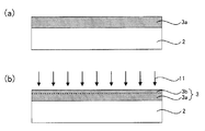
- an amorphous film containing a conductive metal oxide is formed on a transparent substrate, and then the surface of the amorphous film is crystallized by laser annealing to form a crystalline film.
- a method for producing a substrate for a solar cell comprising a transparent electrode layer forming step of obtaining a transparent electrode layer having a film and the crystal film.
- the surface of the amorphous film is crystallized by laser annealing to form a crystalline film, and a transparent electrode layer having an amorphous film and a crystalline film is obtained. It is possible to form a transparent electrode layer that also satisfies the above.
- a heat insulating layer forming step of forming a heat insulating layer on the transparent substrate may be provided before the transparent electrode layer forming step. This is because the transparent substrate can be protected from heat by the heat insulating layer during the laser annealing.
- the transparent substrate has flexibility. It is because a flexible solar cell can be manufactured by using the solar cell substrate obtained by the present invention.
- substrate for solar cells of this invention is a manufacturing method of the board
- the crystalline film is a crystallized amorphous film, it has better acid resistance than the amorphous film. Therefore, a buffer layer forming coating solution that shows acidity is applied onto the transparent electrode layer to buffer the crystalline film.
- a buffer layer forming coating solution that shows acidity is applied onto the transparent electrode layer to buffer the crystalline film.
- the crystal film is an amorphous film crystallized, and the crystal film and the amorphous film have different work functions, so the interface between the transparent electrode layer and the organic layer formed on the transparent electrode layer is different. It is also possible to adjust the work function at.
- the present invention also provides a transparent substrate, a transparent electrode layer formed on the transparent substrate, a buffer layer formed on the transparent electrode layer, a photoelectric conversion layer formed on the buffer layer, and the photoelectric conversion layer.
- a method for producing an organic thin-film solar cell comprising: a buffer layer forming step of forming a buffer layer.
- the present invention provides a transparent substrate, a transparent electrode layer formed on the transparent substrate, a buffer layer formed on the transparent electrode layer, a photoelectric conversion layer formed on the buffer layer, A method for producing an organic thin film solar cell having a counter electrode layer formed on a photoelectric conversion layer, wherein after forming an amorphous film containing a conductive metal oxide on the transparent substrate, the amorphous film A transparent electrode layer forming step of crystallizing the surface of the porous film by laser annealing to form a crystal film and obtaining the transparent electrode layer having the amorphous film and the crystal film; and forming a buffer layer on the transparent electrode layer And a buffer layer forming step of forming a buffer layer by applying a coating liquid for coating.
- a method for producing an organic thin film solar cell is provided.
- the surface of the amorphous film is crystallized by laser annealing to form a crystalline film, and the transparent electrode layer having the amorphous film and the crystalline film is obtained. Therefore, the transparent film having both low resistance and flexibility is obtained.
- An electrode layer can be formed. Since the crystalline film is a crystallized amorphous film, it has better acid resistance than the amorphous film. Therefore, a buffer layer forming coating solution that shows acidity is applied onto the transparent electrode layer to buffer the crystalline film. When forming a layer, it is possible to reduce damage to the transparent electrode layer due to the influence of an acid. Therefore, a highly reliable organic thin film solar cell can be obtained.
- the transparent electrode layer since the transparent electrode layer has an amorphous film and a crystal film containing the same conductive metal oxide, the transparent electrode layer has both low resistance and flexibility, and also has acid resistance. There is an effect that it is possible.
- the substrate for solar cell the solar cell, the organic thin film solar cell, the solar cell module, the organic thin film solar cell module, the method for manufacturing the solar cell substrate, and the method for manufacturing the organic thin film solar cell of the present invention will be described in detail.
- the solar cell substrate of the present invention is a solar cell substrate having a transparent substrate and a transparent electrode layer formed on the transparent substrate, wherein the transparent electrode layer is formed on the transparent substrate and is electrically conductive.
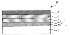
- FIG. 1 is a schematic cross-sectional view showing an example of the solar cell substrate of the present invention.
- a solar cell substrate 1 includes a transparent substrate 2 and a transparent electrode layer 3 formed on the transparent substrate 2 and containing a conductive metal oxide.
- the transparent electrode layer 3 is formed on the transparent substrate 2 and includes an amorphous film 3a containing a conductive metal oxide, and a crystal film 3b formed on the amorphous film 3a and containing a conductive metal oxide. And have.
- the amorphous film 3a and the crystal film 3b contain the same conductive metal oxide, and the crystal film 3b is obtained by crystallizing the surface of the amorphous film 3a.
- a crystalline film has a lower resistance than an amorphous film, that is, has a high conductivity.
- the crystal film has better acid resistance than the amorphous film.
- the work function is different between the amorphous film and the crystal film.
- the transparent electrode layer since the transparent electrode layer has a crystal film having a resistance lower than that of the amorphous film, the conductivity of the transparent electrode layer itself can be increased. Further, since the transparent electrode layer has an amorphous film having excellent flexibility, it is possible to maintain the flexibility of the transparent electrode layer itself. Therefore, in the present invention, a transparent electrode layer having both low resistance and flexibility can be obtained.
- the transparent electrode layer when the transparent substrate is a flexible film substrate, the transparent electrode layer has an amorphous film and is excellent in flexibility. It is possible to obtain a high-performance flexible solar cell by using
- FIG. 2 is a schematic cross-sectional view showing an example of an organic thin-film solar cell having the solar cell substrate of the present invention.
- An organic thin film solar cell 10 shown in FIG. 2 includes a solar cell substrate 1, a buffer layer 4 formed on the transparent electrode layer 3, a photoelectric conversion layer 5 formed on the buffer layer 4, and a photoelectric conversion layer 5.
- the transparent electrode layer has an amorphous film and a crystal film, and the crystal film having excellent acid resistance is formed on the buffer layer side. Therefore, in the organic thin film solar cell as shown in FIG. 2, when the buffer layer contains an acidic material, the buffer layer is not in direct contact with the amorphous film, and the Since the film is protected, damage to the transparent electrode layer due to the influence of the acid contained in the buffer layer can be reduced. Thereby, it can suppress that a transparent electrode layer melt
- FIG. 3 is a schematic cross-sectional view showing another example of an organic thin film solar cell having the solar cell substrate of the present invention.
- the organic thin film solar cell 20 shown in FIG. 3 has a solar cell substrate 1, an organic layer 15 formed on the transparent electrode layer 3, and a counter electrode layer 6 formed on the organic layer 15. .
- the work function is different between the amorphous film and the crystal film of the transparent electrode layer, in the organic thin film solar cell as shown in FIG. 3, the work function is set at the interface between the transparent electrode layer and the organic layer. It is possible to adjust. For example, the difference between the work function of the crystalline film and the work function of the organic layer in direct contact with the transparent electrode layer is greater than the difference between the work function of the amorphous film and the work function of the organic layer in direct contact with the transparent electrode layer. When it is small, the charge mobility from the organic layer to the transparent electrode layer can be improved.
- the transparent electrode layer in the present invention is formed on a transparent substrate, formed on the transparent substrate, and formed on the amorphous film containing the conductive metal oxide and the amorphous film. And a crystalline film containing the same conductive metal oxide as the conductive metal oxide contained in the amorphous film.
- the amorphous film and the crystalline film contain the same conductive metal oxide, and the crystalline film is obtained by crystallizing the surface of the amorphous film. Even if the elemental composition of the conductive metal oxide changes during the process of crystallizing the amorphous film to obtain the crystal film, the conductive metal oxide contained in the amorphous film and the crystal film contain it.
- the conductive metal oxides to be used are the same.
- the transparent electrode layer has an amorphous film and a crystal film by etching the transparent electrode layer.
- the transparent electrode layer is amorphous by comparing the etching rates of the transparent electrode layer, the electrode layer whose whole layer is an amorphous film, and the electrode layer whose whole layer is a crystalline film. It can be confirmed that the film has a film and a crystal film.
- the amount of decrease in the film thickness of the crystal film is smaller than the amount of decrease in the film thickness of the amorphous film.
- the amount of film thickness reduction is measured with a step gauge. The amount of decrease in the thickness of the transparent electrode layer ranges between the amount of decrease in the thickness of the electrode layer whose entire layer is an amorphous film and the amount of decrease in the thickness of the electrode layer whose entire layer is a crystalline film. If it is within the range, the transparent electrode layer is determined to have an amorphous film and a crystalline film.
- the transparent electrode layer is usually an electrode for extracting holes generated in the photoelectric conversion layer (hole extraction electrode).
- the transparent electrode layer has transparency, and the transparent electrode layer side is the light receiving surface.
- Conductive metal oxides used for amorphous films and crystal films are conductive and transparent, have an amorphous structure and a crystal structure, and can have low resistance and high acid resistance due to crystallization. There is no particular limitation as long as it can be crystallized by annealing treatment.
- a conductive metal oxide indium tin oxide (ITO) is preferably used. This is because ITO has conductivity and transparency and has a high work function. Further, when ITO is used, only the layer surface can be crystallized by laser annealing.
- the crystal film preferably has a work function comparable to that when the conductive metal oxide has a crystal structure. That is, it is preferable that the surface of the transparent electrode layer is crystallized until it has a work function comparable to that when the conductive metal oxide has a crystal structure.
- the work function of the crystal film varies depending on the type of conductive metal oxide. For example, when the conductive metal oxide is ITO, the crystal film preferably has a work function of about 4.6 eV to 4.9 eV.
- the work function of the crystal film can be obtained by measuring the work function of the surface of the transparent electrode layer on which the crystal film is formed.
- the sheet resistance of the transparent electrode layer is preferably 100 ⁇ / ⁇ or less, more preferably 50 ⁇ / ⁇ or less, and particularly preferably 20 ⁇ / ⁇ or less. If the sheet resistance of the transparent electrode layer having an amorphous film and a crystal film is in the above range, sufficient conductivity can be obtained. In addition, the said sheet resistance is measured based on JIS R1637 (Resistance test method of fine ceramics thin film: Measurement method by 4 probe method) using a surface resistance meter (Loresta MCP: Four-terminal probe) manufactured by Mitsubishi Chemical Corporation. It is the value.
- the film thickness of the transparent electrode layer is preferably in the range of 0.1 nm to 500 nm, and more preferably in the range of 10 nm to 300 nm. If the film thickness is smaller than the above range, the sheet resistance of the transparent electrode layer may become too large, and the generated charge may not be sufficiently transmitted to the external circuit. This is because the rate may decrease and the photoelectric conversion efficiency may decrease.
- the thickness of the crystal film in the transparent electrode layer may be such that the transparent electrode layer has flexibility. If the crystal film is thick, the flexibility of the transparent electrode layer may be impaired. Therefore, in order to increase the flexibility of the transparent electrode layer, the thickness of the crystal film is preferably relatively thin. Further, when the solar cell substrate of the present invention is an organic thin film solar cell substrate, the thickness of the crystal film in the transparent electrode layer may be any thickness that has acid resistance. If the crystal film is thin, desired acid resistance may not be obtained. On the other hand, if the crystal film is thick, the flexibility of the transparent electrode layer is impaired. If the thickness of the crystal film is equal to or greater than a certain level, sufficient acid resistance can be obtained. Therefore, in order to increase the flexibility of the transparent electrode layer, the thickness of the crystal film is preferably relatively thin among the acid-resistant thicknesses.
- the total light transmittance of the transparent electrode layer is preferably 85% or more, more preferably 90% or more, and particularly preferably 92% or more. This is because when the total light transmittance of the transparent electrode layer is within the above range, light can be sufficiently transmitted through the transparent electrode layer, and light can be efficiently absorbed by the photoelectric conversion layer.
- the total light transmittance is a value measured using an SM color computer (model number: SM-C) manufactured by Suga Test Instruments Co., Ltd. in the visible light region.
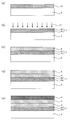
- the transparent electrode layer may be formed on the entire surface of the transparent substrate, or may be formed in a pattern.
- the crystal film 3b may be formed on the entire surface of the amorphous film 3a as illustrated in FIG. 1, and is formed in a pattern on the amorphous film 3a as illustrated in FIG. May be.
- the crystal film is formed in a pattern on the amorphous film, for example, an organic thin film solar cell 10 as shown in FIG. 5 is obtained. Even in such a case, the device performance can be improved.
- Transparent substrate The transparent substrate used in the present invention supports the transparent electrode layer.
- the transparent substrate is not particularly limited.
- inflexible transparent rigid material such as quartz glass, Pyrex (registered trademark), synthetic quartz plate, or flexible resin such as transparent resin film and optical resin plate.
- the transparent flexible material which has property can be mentioned.
- a transparent substrate is flexible materials, such as a transparent resin film. This is because the transparent resin film is excellent in workability, is useful in realizing a reduction in manufacturing cost, weight reduction, and a solar cell that is difficult to break, and expands the applicability to various applications such as application to curved surfaces.
- a barrier layer is formed on the transparent substrate surface.
- an inorganic thin film such as silicon oxide (SiO 2 ), silicon oxynitride (SiON), or silicon nitride (SiN) is generally formed by a vacuum film formation method or the like.
- the barrier layer can be the same as that described in JP-A-2007-73717.
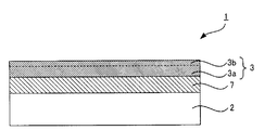
- a heat insulating layer 7 may be formed between the transparent substrate 2 and the transparent electrode layer 3 as illustrated in FIG. This is because when the surface of an amorphous film is crystallized by laser annealing to form a crystal film, the heat insulating layer can protect the transparent substrate from heat.
- a heat insulating layer is preferably formed. Since the heat absorption amount of the film substrate due to laser annealing is reduced by the heat insulating layer, it is possible to prevent the transparent electrode layer from being broken or broken due to the thermal expansion of the film substrate.
- the material for forming the heat insulating layer is not particularly limited as long as it has a low thermal conductivity and heat resistance.
- Preferred examples include silicon oxide (SiO 2 ) and silicon oxynitride (SiON). Etc. This is because a heat insulating layer using these materials also functions as a barrier layer.
- the thickness of the heat insulating layer is not particularly limited as long as it can protect the transparent substrate from the heat during laser annealing, and can be set to about 0.1 ⁇ m to 2 ⁇ m, for example.
- Examples of the method for forming the heat insulating layer include a vapor deposition method such as a sputtering method and a coating method such as a spin coating method.
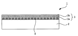
- a patterned auxiliary electrode 8 may be formed between the transparent substrate 2 and the transparent electrode layer 3. Even when the sheet resistance of the transparent electrode layer is relatively high, the resistance of the entire laminate of the transparent electrode layer and the auxiliary electrode can be reduced by sufficiently reducing the sheet resistance of the auxiliary electrode. Therefore, the generated power can be collected efficiently.
- the auxiliary electrode used in the present invention is formed in a pattern on a transparent substrate.
- the auxiliary electrode usually has a lower resistance value than the transparent electrode layer.
- a metal is usually used as a material for forming the auxiliary electrode.
- the metal used for the auxiliary electrode include aluminum (Al), gold (Au), silver (Ag), cobalt (Co), nickel (Ni), platinum (Pt), copper (Cu), and titanium (Ti).
- conductive metals such as iron (Fe), stainless steel, aluminum alloy, copper alloy, titanium alloy, iron-nickel alloy and nickel-chromium alloy (Ni-Cr).
- conductive metals described above those having a relatively low electrical resistance value are preferred. Examples of such a conductive metal include Al, Au, Ag, and Cu.
- the auxiliary electrode may be a single layer made of the conductive metal as described above, and a conductive metal layer and a contact layer are appropriately laminated in order to improve adhesion to the transparent substrate or the transparent electrode layer. It may be what you did.
- the material for forming the contact layer include nickel (Ni), chromium (Cr), nickel chromium (Ni—Cr), titanium (Ti), and tantalum (Ta).
- the contact layer is laminated on the conductive metal layer in order to obtain adhesion between the desired auxiliary electrode and the transparent substrate or transparent electrode layer, and may be laminated only on one side of the conductive metal layer. You may laminate
- the transparent electrode layer is a hole extraction electrode
- the metal used for the auxiliary electrode has a high work function. Specifically, Al is preferably used.
- the shape of the auxiliary electrode is not particularly limited as long as it is a pattern, and is appropriately selected depending on desired conductivity, permeability, strength, and the like.
- the auxiliary electrode may have a mesh-shaped mesh portion and a frame portion arranged around the mesh portion, or may be formed of a mesh-shaped mesh portion.
- the mesh portion and the frame portion may be arranged, for example, when the auxiliary electrode is rectangular, the frame portion may be arranged so as to surround four sides of the mesh portion. Further, it may be arranged so as to surround three sides of the mesh part, may be arranged so as to surround two sides of the mesh part, or may be arranged on one side of the mesh part. Especially, it is preferable that the frame part is arrange
- the shape of the mesh portion is not particularly limited as long as it is a mesh shape, and is appropriately selected depending on desired conductivity, permeability, strength, and the like.
- a polygon such as a triangle, a quadrangle, and a hexagon, a circular lattice, and the like can be given.
- a polygon or circular “lattice shape” refers to a shape in which polygons or circles are periodically arranged.
- polygonal or circular lattice shape for example, polygonal openings may be arranged in a straight line or zigzag.
- the shape of the mesh portion is preferably a hexagonal lattice shape or a parallelogram lattice shape. This is because the current flowing through the mesh portion can be prevented from being concentrated locally.
- the hexagonal openings are arranged in a zigzag (so-called honeycomb shape).
- the acute angle of the parallelogram is preferably within the range of 40 ° to 80 °, more preferably within the range of 50 ° to 70 °, and even more preferably 55 ° to 65 °. Within the range of °.
- the opening of the mesh part of the auxiliary electrode is relatively large.
- the ratio of the openings in the mesh portion of the auxiliary electrode is preferably about 50% to 98%, more preferably in the range of 70% to 98%, and still more preferably in the range of 80% to 98%. Within range.
- the pitch of the openings of the mesh portion of the auxiliary electrode and the line width of the mesh portion are appropriately selected according to the area of the entire auxiliary electrode and the like.
- the line width of the frame portion is appropriately selected according to the area of the entire auxiliary electrode.
- the thickness of the auxiliary electrode is not limited as long as it does not cause a short circuit between the transparent electrode layer and the counter electrode layer.
- the thickness of the auxiliary electrode is not limited to the thickness of the layer formed between the transparent electrode layer and the counter electrode layer. It is selected as appropriate. For example, in the case of an organic thin film solar cell, the thickness of the auxiliary electrode is appropriately selected according to the thickness of the photoelectric conversion layer, the buffer layer, and the like.
- the thickness of the auxiliary electrode is It is preferably 5 or less, more preferably 3 or less, further 2 or less, particularly preferably 1.5 or less, and most preferably 1 or less. This is because if the thickness of the auxiliary electrode is larger than the above range, a short circuit may occur between the electrodes.
- the thickness of the auxiliary electrode is preferably in the range of 100 nm to 1000 nm, more preferably in the range of 200 nm to 800 nm, further in the range of 200 nm to 500 nm, particularly in the range of 200 nm to 400 nm. It is preferable. This is because if the thickness of the auxiliary electrode is thinner than the above range, the sheet resistance of the auxiliary electrode may become too large. Moreover, it is because there exists a possibility that a short circuit may arise between electrodes when the thickness of an auxiliary electrode is thicker than the said range.
- the photoelectric conversion layer is formed on the transparent electrode layer by a method capable of adjusting the thickness mainly in accordance with the coating amount.
- the thickness of the auxiliary electrode is preferably in the range of 200 nm to 300 nm.
- the photoelectric conversion layer may be formed thicker than the desired thickness due to surface tension. If the thickness of the photoelectric conversion layer is too thick, it exceeds the electron diffusion length and the hole diffusion length, and the conversion efficiency decreases. It is preferable to adjust the thickness of the auxiliary electrode so that the photoelectric conversion layer is not formed thicker than desired due to surface tension. In particular, since it is known that the distance that holes and electrons can move in the photoelectric conversion layer is about 100 nm, the auxiliary electrode is formed so that the photoelectric conversion layer is not formed thicker than the desired thickness due to surface tension. It is preferable to adjust the thickness.
- the photoelectric conversion layer is formed by, for example, a spin coating method
- a uniform film is formed by centrifugal force, so that the edge of the auxiliary electrode can be covered even if the auxiliary electrode is relatively thick.
- the thickness can be adjusted by the number of rotations, so that a uniform film can be obtained even if the auxiliary electrode is relatively thick. Therefore, when the photoelectric conversion layer is formed mainly by a method capable of adjusting the thickness according to the coating amount, the above range is particularly preferable.
- the sheet resistance of the auxiliary electrode may be lower than that of the transparent electrode layer.
- the sheet resistance of the auxiliary electrode is preferably 5 ⁇ / ⁇ or less, more preferably 3 ⁇ / ⁇ or less, more preferably 1 ⁇ / ⁇ or less, particularly preferably 0.5 ⁇ / ⁇ or less, and 0.1 ⁇ . Most preferably, it is less than / ⁇ . This is because if the sheet resistance of the auxiliary electrode is larger than the above range, desired power generation efficiency may not be obtained.
- the said sheet resistance is measured based on JIS R1637 (Resistance test method of fine ceramics thin film: Measurement method by 4 probe method) using a surface resistance meter (Loresta MCP: Four-terminal probe) manufactured by Mitsubishi Chemical Corporation. It is the value.
- the method for forming the auxiliary electrode is not particularly limited, and examples thereof include a method in which a metal thin film is formed on the entire surface and then patterned in a mesh shape, and a method in which a mesh-like conductor is directly formed. These methods are appropriately selected depending on the auxiliary electrode forming material, configuration, and the like.
- the method for forming the metal thin film is preferably a vacuum film forming method such as a vacuum deposition method, a sputtering method, or an ion plating method. That is, the auxiliary electrode is preferably a metal thin film formed by a vacuum film forming method.
- the metal species formed by the vacuum film formation method has less inclusions than the plating film and can reduce the specific resistance, and can also reduce the specific resistance as compared with those formed using Ag paste or the like.
- a vacuum film formation method is also suitable as a method for forming a metal thin film having a thickness of 1 ⁇ m or less, preferably 500 nm or less, with a precise thickness and a uniform thickness.
- the method for patterning the metal thin film is not particularly limited as long as it can be accurately formed into a desired pattern, and examples thereof include a photoetching method.
- the solar cell substrate of the present invention is used for solar cells in general, and can be used for organic thin film solar cells, dye-sensitized solar cells, compound semiconductor solar cells, silicon solar cells, and the like. .
- substrate for solar cells of this invention is used for an organic thin film solar cell, a dye-sensitized solar cell, a compound semiconductor solar cell, and an amorphous silicon solar cell. Since these solar cells have relatively high resistance to bending, they are suitable as flexible solar cells and are suitable for the solar cell substrate of the present invention.
- the solar cell substrate of the present invention is preferably an organic thin film solar cell substrate.
- the resistance of the transparent electrode layer can be reduced, damage to the transparent electrode layer due to acid can be suppressed, and electrical characteristics can be improved.
- the solar cell of the present invention includes the above-described solar cell substrate.
- the solar cell substrate is provided, a transparent electrode layer having both low resistance and flexibility can be obtained. Further, when the transparent substrate is a flexible film substrate, the transparent electrode layer has an amorphous film and is excellent in flexibility, so that a high-performance flexible solar cell can be obtained. is there.
- the type of the solar cell of the present invention is not particularly limited, and examples thereof include an organic thin film solar cell, a dye-sensitized solar cell, a compound semiconductor solar cell, and a silicon solar cell.
- compound semiconductor solar cells include III-V compound semiconductor solar cells such as gallium arsenide (GaAs) and indium phosphorus (InP), and II-VI compound semiconductor solar cells such as cadmium tellurium (CdTe).
- III-V compound semiconductor solar cells such as gallium arsenide (GaAs) and indium phosphorus (InP)
- II-VI compound semiconductor solar cells such as cadmium tellurium (CdTe).
- Examples include batteries, I-III-VI group compound semiconductor solar cells such as CIS (CuInSe 2 ) and CIGS (Cu (In, Ga) Se 2 ).
- the silicon-based solar cell examples include a single crystal silicon solar cell, a polycrystalline silicon solar cell, and a single junction type or tandem structure type amorphous silicon solar cell.
- a thin film polycrystalline silicon solar cell, a thin film microcrystalline silicon solar cell, a hybrid solar cell of a thin film crystalline silicon solar cell and an amorphous silicon solar cell can also be mentioned.
- the solar cell of the present invention is preferably an organic thin film solar cell, a dye-sensitized solar cell, a compound semiconductor solar cell, or an amorphous silicon solar cell. This is because these solar cells have a relatively high resistance to bending, and thus are suitable as flexible solar cells and useful.
- An organic thin film solar cell is particularly suitable. This is because the acid resistance can be improved in the present invention as described above.
- the organic thin film solar cell the dye-sensitized solar cell, the compound semiconductor solar cell, and the silicon solar cell will be described separately.
- Organic thin-film solar cell of the present invention comprises the above-described solar cell substrate, a solar cell substrate, a photoelectric conversion layer formed on the transparent electrode layer of the solar cell substrate, A counter electrode layer formed on the photoelectric conversion layer.
- the solar cell substrate has been described in detail in the section “A. Solar Cell Substrate” above, and will not be described here.
- the organic thin film solar cell will be described in detail in the section “C. Organic thin film solar cell” described later, and the description thereof will be omitted here.
- the dye-sensitized solar cell of the present invention includes the above-described solar cell substrate, and is formed, for example, on the solar cell substrate and the transparent electrode layer of the solar cell substrate.
- the solar cell substrate has been described in detail in the section “A. Solar Cell Substrate” above, and will not be described here. Hereinafter, other configurations in the dye-sensitized solar cell will be described.
- Porous layer contains oxide semiconductor fine particles carrying a dye sensitizer.
- oxide semiconductor fine particles carrying a dye sensitizer carrying a dye sensitizer.
- the oxide semiconductor fine particles are not particularly limited as long as they are made of an oxide having semiconductor characteristics.
- the oxide constituting the oxide semiconductor fine particles include TiO 2 , ZnO, SnO 2 , ITO, ZrO 2 , MgO, Al 2 O 3 , CeO 2 , Bi 2 O 3 , Mn 3 O 4 , and Y 2 O. 3 , WO 3 , Ta 2 O 5 , Nb 2 O 5 , La 2 O 3 and the like.
- These oxide semiconductor fine particles are suitable for forming a porous porous layer, and are preferably used because energy conversion efficiency can be improved and cost can be reduced.
- the oxide semiconductor fine particles may all be made of the same oxide, or two or more kinds of oxide semiconductor fine particles may be used.
- One kind of oxide semiconductor fine particles may be a core fine particle, and another oxide semiconductor may have a core-shell structure including a core fine particle to form a shell.
- oxide semiconductor fine particles made of TiO 2 it is most preferable to use oxide semiconductor fine particles made of TiO 2 . This is because TiO 2 is particularly excellent in semiconductor characteristics.
- the average particle diameter of the oxide semiconductor fine particles is not particularly limited as long as the specific surface area of the porous layer is within a desired range, but is preferably within a range of 1 nm to 10 ⁇ m, and particularly 10 nm to 1000 nm. It is preferable to be within the range. If the average particle size is smaller than the above range, the respective oxide semiconductor fine particles may aggregate to form secondary particles. If the average particle size is larger than the above range, the porous layer becomes thicker. This is because the porosity of the porous layer, that is, the specific surface area may be reduced. Here, when the specific surface area of the porous layer becomes small, for example, it may be difficult to carry a dye sensitizer sufficient for photoelectric conversion on the porous layer. Note that the average particle size of the oxide semiconductor fine particles means a primary particle size.
- oxide semiconductor fine particles those having the same average particle diameter may be used, or a plurality of oxide semiconductor fine particles having different average particle diameters may be used.
- oxide semiconductor fine particles having different average particle diameters By using together oxide semiconductor fine particles having different average particle diameters, the light scattering effect in the porous layer can be enhanced, and there is an advantage that the dye-sensitized solar cell can be made more excellent in power generation efficiency.
- the combination of the different average particle diameters is, for example, oxide semiconductor fine particles having an average particle diameter in the range of 10 nm to 50 nm and an average particle diameter of 50 nm.
- oxide semiconductor fine particles in the range of ⁇ 800 nm can be exemplified.
- the dye sensitizer is not particularly limited as long as it can absorb light and generate an electromotive force.
- a dye sensitizer include organic dyes and metal complex dyes.
- the organic dye include acridine, azo, indigo, quinone, coumarin, merocyanine, and phenylxanthene dyes. Among these organic dyes, it is preferable to use a coumarin dye.
- the metal complex dye it is preferable to use a ruthenium dye, and it is particularly preferable to use a ruthenium bipyridine dye and a ruthenium terpyridine dye which are ruthenium complexes. This is because such a ruthenium complex has a wide wavelength range of light to be absorbed, so that the wavelength range of light that can be photoelectrically converted can be greatly expanded.
- the porous layer may contain an optional component in addition to the oxide semiconductor fine particles.
- binder resin can be mentioned, for example. It is because a porous layer can be made into a thing with low brittleness by containing binder resin in a porous layer.
- the binder resin is not particularly limited as long as the brittleness of the porous layer can be set to a desired level. However, since the porous layer is formed in contact with the electrolyte layer as described later, it is necessary to use a binder resin having resistance to the electrolyte layer.
- a binder resin include polyvinyl pyrrolidone, ethyl cellulose, caprolactan, and the like. There may be only one type of binder resin, or two or more types.
- the thickness of the porous layer is appropriately selected according to the use of the dye-sensitized solar cell and is not particularly limited.
- the thickness of the porous layer is preferably in the range of 1 ⁇ m to 100 ⁇ m, and particularly preferably in the range of 3 ⁇ m to 30 ⁇ m. This is because if the thickness of the porous layer is larger than the above range, the porous layer itself tends to cause cohesive failure, which tends to cause membrane resistance.
- the thickness of the porous layer is thinner than the above range, it becomes difficult to form a porous layer having a uniform thickness, or the amount of the dye sensitizer carried is reduced, so that the sunlight is sufficiently absorbed. This is because there is a possibility that performance may be deteriorated because it is not possible.
- the porous layer may be formed on one surface or a pattern on the solar cell substrate.
- the method for forming the porous layer can be the same as the general method for forming a porous layer in a dye-sensitized solar cell.
- Electrolyte layer The electrolyte layer is formed so as to be in contact with the porous layer between the transparent electrode layer and the counter electrode layer of the solar cell substrate.
- the electrolyte layer may be in any form of gel, solid or liquid.
- the electrolyte layer may or may not contain a redox pair.
- the redox couple is not particularly limited as long as it is generally used in an electrolyte layer of a dye-sensitized solar cell. A combination, a combination of bromine and bromide is preferred.
- Examples of the combination of iodine and iodide are used as the redox pair may be, for example, LiI, NaI, KI, and metal iodide such as CaI 2, a combination of I 2.
- Examples of the combination of bromine and bromide include a combination of a metal bromide such as LiBr, NaBr, KBr, CaBr 2 and Br 2 .
- the electrolyte layer When the electrolyte layer is in a liquid state, for example, acetonitrile, methoxyacetonitrile, propylene carbonate or the like is used as a solvent, and a redox couple containing the same or an ionic liquid having an imidazolium salt as a cation is used as the solvent. Can do.
- the electrolyte layer when it is in a gel form, it may be either a physical gel or a chemical gel.
- the physical gel is gelled near room temperature due to physical interaction
- the chemical gel is a gel formed by chemical bonding by a crosslinking reaction or the like.
- a solid electrolyte layer what consists of CuI, a polypyrrole, polythiophene etc. can be mentioned, for example.
- a catalyst layer may be formed between the counter electrode layer, the porous layer, and the electrolyte layer as necessary.
- the catalyst layer By forming the catalyst layer on the counter electrode layer, the dye-sensitized solar cell can be made more excellent in power generation efficiency.
- examples of such a catalyst layer include an embodiment in which Pt is deposited on the counter electrode layer, polyethylene dioxythiophene (PEDOT), polystyrene sulfonic acid (PSS), polyaniline (PA), paratoluene sulfonic acid (PTS) and Although the aspect which forms a catalyst layer from these mixtures can be mentioned, it is not this limitation.
- a sealant layer may be formed for sealing.
- the sealing agent used for the sealing agent layer is not particularly limited as long as it has durability to the electrolyte layer.
- various thermoplastic resins and thermoplastic elastomers that can be heat sealed, low density Random or block co-polymerization of ⁇ -olefins such as polyethylene, high-density polyethylene, polypropylene, poly-1-butene, poly-4-methyl-1-pentene, or ethylene, propylene, 1-butene, 4-methyl-1-pentene
- Polyolefin resins such as copolymers; ethylene-vinyl compound copolymer resins such as ethylene-vinyl acetate copolymer, ethylene-vinyl alcohol copolymer, ethylene-vinyl chloride copolymer; polystyrene, acrylonitrile-styrene copolymer, Styrene such as ABS, ⁇ -methyl
- the thickness of the sealing agent layer is preferably in the range of 1 ⁇ m to 100 ⁇ m, and more preferably in the range of 1 ⁇ m to 50 ⁇ m.
- the counter electrode layer can be the same as the counter electrode layer in the organic thin film solar cell described later.
- the counter electrode layer may be formed on the counter substrate.
- the counter substrate can be the same as the above-described transparent substrate of the solar cell substrate, and thus description thereof is omitted here.
- the compound semiconductor solar cell of the present invention includes the above-described solar cell substrate, and is formed on the solar cell substrate and the transparent electrode layer of the solar cell substrate. It has a semiconductor layer to be contained and a counter electrode layer disposed on the semiconductor layer.
- the solar cell substrate has been described in detail in the section “A. Solar Cell Substrate” above, and will not be described here. Hereinafter, other configurations of the compound semiconductor solar cell will be described.
- a semiconductor layer is a layer containing a compound semiconductor.
- compound semiconductors include III-V group compound semiconductors such as gallium arsenide (GaAs) and indium phosphorus (InP), II-VI group compound semiconductors such as cadmium tellurium (CdTe), CIS (CuInSe 2 ), and CIGS (Cu Examples include I-III-VI group compound semiconductors such as (In, Ga) Se 2 ).
- Counter electrode layer The counter electrode layer can be the same as the counter electrode layer in the organic thin film solar cell described later.
- Silicon-based solar cell The silicon-based solar cell of the present invention includes the above-described solar cell substrate, and is a semiconductor that is formed on the solar cell substrate and the transparent electrode layer of the solar cell substrate and contains silicon. And a counter electrode layer disposed on the semiconductor layer.
- the solar cell substrate has been described in detail in the section “A. Solar Cell Substrate” above, and will not be described here. Hereinafter, other configurations of the silicon-based solar cell will be described.
- the semiconductor layer is a layer containing silicon.
- silicon include single crystal silicon, polycrystalline silicon, and amorphous silicon.
- the semiconductor layer may be a stack of a layer containing thin film polycrystalline silicon, thin film microcrystalline silicon, or thin film crystal silicon, and a layer containing amorphous silicon. In this case, a hybrid solar cell can be obtained.
- Counter electrode layer The counter electrode layer can be the same as the counter electrode layer in the organic thin film solar cell described later.
- the organic thin film solar cell of the present invention includes a transparent substrate, a transparent electrode layer formed on the transparent substrate, a buffer layer formed on the transparent electrode layer, and a photoelectric conversion layer formed on the buffer layer. And a counter electrode layer formed on the photoelectric conversion layer, wherein the transparent electrode layer is an amorphous material formed on the transparent substrate and containing a conductive metal oxide. And a crystalline film formed on the amorphous film and containing the same conductive metal oxide as the conductive metal oxide contained in the amorphous film. It is. That is, the organic thin-film solar cell of the present invention includes the above-described solar cell substrate, and a buffer layer is formed on the transparent electrode layer.
- FIG. 2 is a schematic cross-sectional view showing an example of the organic thin film solar cell of the present invention.
- the organic thin-film solar cell 10 includes a solar cell substrate 1, a buffer layer 4 formed on the transparent electrode layer 3 of the solar cell substrate 1, and a photoelectric film formed on the buffer layer 4. It has a conversion layer 5 and a counter electrode layer 6 formed on the photoelectric conversion layer 5.
- the solar cell substrate 1 has a transparent substrate 2 and a transparent electrode layer 3 formed on the transparent substrate 2 and containing a conductive metal oxide.
- the transparent electrode layer 3 is formed on the transparent substrate 2 and is formed on the amorphous film 3a containing the conductive metal oxide and in contact with the buffer layer 4 on the amorphous film 3a. And a crystal film 3b containing.
- the amorphous film 3a and the crystal film 3b contain the same conductive metal oxide, and the crystal film 3b is obtained by crystallizing the surface of the amorphous film 3a.
- the solar cell substrate is provided, a transparent electrode layer having both low resistance and flexibility can be obtained. Further, when the transparent substrate is a flexible film substrate, the transparent electrode layer has an amorphous film and is excellent in flexibility, so that a high-performance flexible organic thin film solar cell can be obtained. Is possible.
- the solar cell substrate since the solar cell substrate is included, when the buffer layer contains a material exhibiting acidity, it is due to the influence of the acid contained in the buffer layer when the buffer layer is formed and when the solar cell is used. It is possible to reduce damage to the transparent electrode layer. Thereby, it is possible to suppress the deterioration of the electrical characteristics of the transparent electrode layer and to improve the reliability of the organic thin film solar cell.
- the transparent substrate, the transparent electrode layer, the heat insulating layer, and the auxiliary electrode have been described in detail in the above section “A. Solar Cell Substrate”, and thus description thereof is omitted here.
- the other structure in the organic thin-film solar cell of this invention is demonstrated.
- Buffer layer The buffer layer in the present invention is formed directly on the transparent electrode layer, and is a layer provided so that the charge can be easily taken out from the photoelectric conversion layer to the transparent electrode layer. Since the transparent electrode layer is usually a hole extraction electrode, the buffer layer is preferably a layer provided so that holes can be easily extracted from the photoelectric conversion layer to the transparent electrode layer. Since the hole extraction efficiency from the photoelectric conversion layer to the transparent electrode layer is increased by the buffer layer, the photoelectric conversion efficiency can be improved.
- the material used for the buffer layer is not particularly limited as long as it is a material that stabilizes the extraction of holes from the photoelectric conversion layer to the transparent electrode layer.
- conductive organic compounds such as doped polyaniline, polyphenylene vinylene, polythiophene, polypyrrole, polyparaphenylene, polyacetylene, triphenyldiamine (TPD), or electron donation such as tetrathiofulvalene, tetramethylphenylenediamine, etc.
- An organic material that forms a charge transfer complex composed of an organic compound and an electron-accepting compound such as tetracyanoquinodimethane and tetracyanoethylene.
- PEDOT / PSS polyethylene dioxythiophene / polystyrene sulfonic acid
- the material used for a buffer layer is what shows acidity. Specifically, a material having a pH of less than 7 when used as a coating solution is preferable. As described above, when the buffer layer contains a material exhibiting acidity, the damage of the transparent electrode layer due to the influence of the acid contained in the buffer layer can be reduced, so the configuration of the present invention is useful. Examples of the material showing acidity include PEDOT / PSS and doped polyaniline, and PEDOT / PSS is particularly preferably used. That is, the buffer layer preferably contains PEDOT / PSS. PEDOT / PSS is a material that exhibits acidity in the coating liquid for forming the buffer layer, and also exhibits acidity in the buffer layer when the buffer layer absorbs moisture. Therefore, it is useful that the transparent electrode layer has a crystal film on the buffer layer side as in the configuration of the present invention.
- the thickness of the buffer layer is preferably in the range of 10 nm to 200 nm.
- the photoelectric conversion layer used in the present invention is formed between the transparent electrode layer and the counter electrode layer.
- the “photoelectric conversion layer” refers to a member that contributes to charge separation of the organic thin film solar cell and has a function of transporting generated electrons and holes toward electrodes in opposite directions.
- the photoelectric conversion layer may be a single layer having both an electron-accepting function and an electron-donating function (first aspect), or an electron-accepting layer having an electron-accepting function and an electron-donating function.
- a layer in which an electron donating layer having n is laminated may be used (second embodiment).
- the 1st aspect of the photoelectric converting layer in this invention is a single layer which has both an electron-accepting function and an electron-donating function, and contains an electron-donating material and an electron-accepting material It is.
- this photoelectric conversion layer since charge separation occurs using a pn junction formed in the photoelectric conversion layer, it functions as a photoelectric conversion layer alone.
- the electron donating material is not particularly limited as long as it has a function as an electron donor, but it is preferable that the material can be formed by a wet coating method.
- a polymer material is preferred.
- a conductive polymer is a so-called ⁇ -conjugated polymer, which is composed of a ⁇ -conjugated system in which double bonds or triple bonds containing carbon-carbon or hetero atoms are alternately linked to single bonds, and exhibits semiconducting properties. It is. In the conductive polymer material, ⁇ conjugation is developed in the polymer main chain, so that charge transport in the main chain direction is basically advantageous.
- the electron transfer mechanism of the conductive polymer is mainly hopping conduction between molecules by ⁇ stacking, it is advantageous not only for the main chain direction of the polymer but also for the charge transport in the film thickness direction of the photoelectric conversion layer. is there.
- the conductive polymer material can be easily formed by a wet coating method using a coating solution in which the conductive polymer material is dissolved or dispersed in a solvent, a large-area organic thin film solar cell Can be manufactured at low cost without requiring expensive equipment.
- Examples of the electron-donating conductive polymer material include polyphenylene, polyphenylene vinylene, polysilane, polythiophene, polycarbazole, polyvinyl carbazole, porphyrin, polyacetylene, polypyrrole, polyaniline, polyfluorene, polyvinyl pyrene, polyvinyl anthracene, and derivatives thereof. And copolymers thereof, or phthalocyanine-containing polymers, carbazole-containing polymers, organometallic polymers, and the like.
- thiophene-fluorene copolymer polyalkylthiophene, phenylene ethynylene-phenylene vinylene copolymer, phenylene ethynylene-thiophene copolymer, phenylene ethynylene-fluorene copolymer, fluorene-phenylene vinylene copolymer
- a thiophene-phenylene vinylene copolymer is preferably used. This is because the energy level difference is appropriate for many electron-accepting materials.
- a phenylene ethynylene-phenylene vinylene copolymer Poly [1,4-phenyleneethynylene-1,4- (2,5-dioctadodecyloxyphenylene) -1,4-phenyleneethene-1,2-diyl-1,4- ( 2,5-dioctadodecyloxyphenylene) ethene-1,2-diyl]
- the electron-accepting material is not particularly limited as long as it has a function as an electron acceptor, but it is preferable that it can be formed into a film by a wet coating method.
- a conductive polymer material is preferable. This is because the conductive polymer material has the advantages as described above.
- Examples of the electron-accepting conductive polymer material include polyphenylene vinylene, polyfluorene, and derivatives thereof, and copolymers thereof, or carbon nanotubes, fullerene derivatives, CN group or CF 3 group-containing polymers, and the like. And —CF 3 substituted polymer.
- polyphenylene vinylene derivative examples include CN-PPV (Poly [2-Methoxy-5- (2′-ethylhexyloxy) -1,4- (1-cyanovinylene) phenylene]), MEH-CN-PPV (Poly [2 -Methoxy-5- (2′-ethylhexyloxy) -1,4- (1-cyanovinylene) phenylene]) and the like.
- an electron accepting material doped with an electron donating compound, an electron donating material doped with an electron accepting compound, or the like can be used.
- a conductive polymer material doped with an electron donating compound or an electron accepting compound is preferably used.
- Conductive polymer materials are basically advantageous in charge transport in the direction of the main chain because of the development of ⁇ conjugation in the polymer main chain, and are doped with electron-donating compounds and electron-accepting compounds. This is because electric charges are generated in the ⁇ -conjugated main chain, and the electrical conductivity can be greatly increased.
- Examples of the electron-accepting conductive polymer material doped with the electron-donating compound include the above-described electron-accepting conductive polymer material.
- a Lewis base such as an alkali metal such as Li, K, Ca, or Cs or an alkaline earth metal can be used.
- the Lewis base acts as an electron donor.
- the electron-donating conductive polymer material doped with the electron-accepting compound include the above-described electron-donating conductive polymer material.
- a Lewis acid such as FeCl 3 (III), AlCl 3 , AlBr 3 , AsF 6 or a halogen compound can be used. In addition, Lewis acid acts as an electron acceptor.
- the film thickness of the photoelectric conversion layer As the film thickness of the photoelectric conversion layer, the film thickness generally employed in bulk heterojunction organic thin-film solar cells can be employed. Specifically, it can be set within the range of 0.2 nm to 3000 nm, and preferably within the range of 1 nm to 600 nm. This is because when the film thickness is thicker than the above range, the volume resistance in the photoelectric conversion layer may increase. On the other hand, if the film thickness is thinner than the above range, light may not be sufficiently absorbed.
- the mixing ratio of the electron-donating material and the electron-accepting material is appropriately adjusted to an optimal mixing ratio depending on the type of material used.
- the method for forming the photoelectric conversion layer is not particularly limited as long as it can be uniformly formed in a predetermined film thickness, but a wet coating method is preferably used. This is because if the wet coating method is used, the photoelectric conversion layer can be formed in the air, and the cost can be reduced and the area can be easily increased.
- the method for applying the photoelectric conversion layer coating liquid is not particularly limited as long as it can uniformly apply the photoelectric conversion layer coating liquid.
- a die coating method, a spin coating method, a dip coating, and the like examples thereof include a coating method, a roll coating method, a bead coating method, a spray coating method, a bar coating method, a gravure coating method, an ink jet method, a screen printing method, and an offset printing method.
- coating method of the coating liquid for photoelectric conversion layers is a method which can adjust thickness mainly according to the application amount.
- Methods that can adjust the thickness mainly according to the coating amount include, for example, a die coating method, a bead coating method, a bar coating method, a gravure coating method, an ink jet method, a screen printing method, and an offset printing method. Can be mentioned.
- the printing method is suitable for increasing the area of the organic thin film solar cell.
- a drying treatment for drying the formed coating film may be performed. It is because productivity can be improved by removing the solvent etc. which are contained in the coating liquid for photoelectric conversion layers at an early stage.
- a drying method for example, a general method such as heat drying, air drying, vacuum drying, infrared heat drying, or the like can be used.
- the electron-accepting layer used in this embodiment has an electron-accepting function and contains an electron-accepting material.
- the electron-accepting material is not particularly limited as long as it has a function as an electron acceptor, but is preferably a material that can be formed into a film by a wet coating method.
- a polymer material is preferred. This is because the conductive polymer material has the advantages as described above. Specific examples include the same electron-accepting conductive polymer materials used for the photoelectric conversion layer of the first aspect.
- a film thickness generally employed in a bilayer type organic thin film solar cell can be employed. Specifically, it can be set within a range of 0.1 nm to 1500 nm, and preferably within a range of 1 nm to 300 nm. This is because if the film thickness is larger than the above range, the volume resistance in the electron-accepting layer may be increased. On the other hand, if the film thickness is thinner than the above range, light may not be sufficiently absorbed.
- the method for forming the electron-accepting layer can be the same as the method for forming the photoelectric conversion layer of the first aspect.
- the electron donating layer used in this embodiment has an electron donating function and contains an electron donating material.
- the electron donating material is not particularly limited as long as it has a function as an electron donor, but it is preferable that the material can be formed by a wet coating method.
- a polymer material is preferred. This is because the conductive polymer material has the advantages as described above. Specific examples include the same electron donating conductive polymer materials used for the photoelectric conversion layer of the first aspect.
- a film thickness generally employed in a bilayer type organic thin film solar cell can be employed. Specifically, it can be set within a range of 0.1 nm to 1500 nm, and preferably within a range of 1 nm to 300 nm. This is because if the film thickness is larger than the above range, the volume resistance in the electron donating layer may be increased. On the other hand, if the film thickness is thinner than the above range, light may not be sufficiently absorbed.
- the method for forming the electron donating layer can be the same as the method for forming the photoelectric conversion layer of the first aspect.
- the counter electrode layer used in the present invention is an electrode facing the transparent electrode layer.
- the counter electrode layer is an electrode (electron extraction electrode) for extracting electrons generated in the photoelectric conversion layer.
- the counter electrode layer since the transparent electrode layer side becomes the light receiving surface, the counter electrode layer may or may not have transparency.
- the material for forming the counter electrode layer is not particularly limited as long as it has conductivity. However, since the counter electrode layer is an electron extraction electrode, it preferably has a low work function. Specific examples of the material having a low work function include Li, In, Al, Ag, Ca, Mg, Sm, Tb, Yb, Zr, and LiF.
- the counter electrode layer may be a single layer or may be laminated using materials having different work functions. Examples of the counter electrode layer in which different materials are laminated include those in which any one of Ca, LiF, LiCa, MoO 3 or VO 5 and any one of Al or Ag are laminated.
- the thickness of the counter electrode layer is within a range of 0.1 nm to 500 nm, particularly 1 nm to 300 nm. It is preferable to be within the range.
- the film thickness is thinner than the above range, the sheet resistance of the counter electrode layer becomes too large, and the generated charge may not be sufficiently transmitted to the external circuit.
- the counter electrode layer may be formed on the entire surface of the photoelectric conversion layer, or may be formed in a pattern.
- a method for forming the counter electrode layer a general electrode forming method can be used. For example, a vacuum evaporation method or a pattern evaporation method using a metal mask can be used.
- an electron extraction layer may be formed between the photoelectric conversion layer and the counter electrode layer.
- the electron extraction layer is a layer provided so that electrons can be easily extracted from the photoelectric conversion layer to the electron extraction electrode. Thereby, since the electron extraction efficiency from the photoelectric conversion layer to the electron extraction electrode is increased, the photoelectric conversion efficiency can be improved.
- the material used for the electron extraction layer is not particularly limited as long as it is a material that stabilizes the extraction of electrons from the photoelectric conversion layer to the electron extraction electrode.
- conductive organic compounds such as doped polyaniline, polyphenylene vinylene, polythiophene, polypyrrole, polyparaphenylene, polyacetylene, triphenyldiamine (TPD), or electron donation such as tetrathiofulvalene, tetramethylphenylenediamine, etc.
- An organic material that forms a charge transfer complex composed of an organic compound and an electron-accepting compound such as tetracyanoquinodimethane and tetracyanoethylene.
- the metal dope layer with an alkali metal or alkaline-earth metal is mentioned.
- Suitable materials include bathocuproin (BCP) or bathophenantrone (Bphen) and metal doped layers such as Li, Cs, Ba, Sr.
- the organic thin film solar cell of the present invention may have constituent members to be described later as necessary in addition to the constituent members described above.
- the organic thin film solar cell of the present invention is a functional layer such as a protective sheet, a filler layer, a barrier layer, a protective hard coat layer, a strength support layer, an antifouling layer, a high light reflection layer, a light containment layer, a sealing material layer, etc. You may have.
- an adhesive layer may be formed between the functional layers depending on the layer configuration. These functional layers can be the same as those described in JP-A-2007-73717.
- the solar cell module of the present invention is characterized in that a plurality of the above-described solar cells are connected in series or in parallel.
- the connection of a plurality of solar cells is not limited as long as a desired electromotive force can be obtained, may be only in series, only in parallel, or a combination of series and parallel.
- B. Solar cell about the solar cell, description here is abbreviate
- Organic thin film solar cell module The organic thin film solar cell module of the present invention is characterized in that a plurality of the above organic thin film solar cells are connected in series or in parallel.
- the connection of the plurality of organic thin-film solar cells is not limited as long as a desired electromotive force can be obtained, may be only in series, may be only in parallel, or may be a combination of series and parallel. Since the organic thin film solar cell is described in detail in the section “C. Organic thin film solar cell”, description thereof is omitted here.
- an amorphous film containing a conductive metal oxide is formed on a transparent substrate, and then the surface of the amorphous film is crystallized by laser annealing to form a crystalline film. It has a transparent electrode layer forming step of forming and obtaining a transparent electrode layer having the amorphous film and the crystal film.
- FIG. 8A to 8 (b) are process charts showing an example of a method for manufacturing a solar cell substrate of the present invention.
- an amorphous film 3 a containing a conductive metal oxide is formed on the transparent substrate 2.
- the surface of the amorphous film 3a is crystallized by irradiating the laser 11 to form a crystal film 3b. Since the crystal film 3b is obtained by crystallizing the surface of the amorphous film 3a, the crystal film 3b has a lower resistance and superior acid resistance than the amorphous film 3a. Thereby, the transparent electrode layer 3 having the amorphous film 3a and the crystal film 3b is obtained (transparent electrode layer forming step).
- the transparent electrode layer since the surface of the amorphous film is crystallized by laser annealing to form a crystalline film having a lower resistance than the amorphous film, it is possible to obtain a transparent electrode layer with good conductivity. Moreover, since only the surface of the amorphous film is crystallized by laser annealing to form a crystal film, the transparent electrode layer has an amorphous film having excellent flexibility, and the transparent electrode layer having flexibility It is possible to obtain Therefore, in the present invention, a transparent electrode layer having both low resistance and flexibility can be formed.
- a transparent substrate with low heat resistance is used. It is possible. Therefore, a flexible film substrate can be used as the transparent substrate. As described above, in the present invention, a flexible transparent electrode layer can be obtained, and a flexible film substrate can be used as the transparent substrate. Therefore, a high-performance flexible solar cell can be manufactured. Is possible.
- the surface of the amorphous film is crystallized by laser annealing to form a crystalline film, for example, when an organic thin film solar cell 10 as shown in FIG.
- the buffer layer 4 is not directly formed. Therefore, when the buffer layer is formed using an acidic material, the amorphous film is protected by the crystal film, and it is possible to reduce the damage of the transparent electrode layer due to the influence of the acid contained in the buffer layer. is there. Thereby, it becomes possible to obtain an organic thin film solar cell with high reliability. Therefore, in the present invention, it is possible to produce an organic thin-film solar cell excellent in electrical performance by reducing the resistance of the transparent electrode layer and suppressing damage to the transparent electrode layer due to acid.
- the surface of the amorphous film is crystallized by laser annealing to form a crystalline film having a work function different from that of the amorphous film, and thus, for example, an organic thin film solar cell 20 as shown in FIG.
- Transparent electrode layer forming step In the transparent electrode layer forming step in the present invention, an amorphous film containing a conductive metal oxide is formed on a transparent substrate, and then the surface of the amorphous film is crystallized by laser annealing. This is a step of forming a crystal film and obtaining a transparent electrode layer having the amorphous film and the crystal film.
- the method for forming the amorphous film is not particularly limited as long as it is a method capable of forming a film having an amorphous structure.
- a sputtering method a vacuum evaporation method, an ion plating method, a thermal CVD method is used. And plasma CVD method.
- the sputtering method is preferable.
- an excimer laser can be used as the laser.
- the excimer laser include a KrF excimer laser (wavelength 248 nm), an ArF excimer laser (wavelength 193 nm), and the like.
- a KrF excimer laser having a wavelength of 248 nm is preferably used because of its versatility.
- the laser irradiation conditions are appropriately adjusted according to the damage to the amorphous film and the crystallinity of the irradiated portion.
- the output of the laser can be in a range of 70mJ / cm 2 ⁇ 110mJ / cm 2, the range among them of 80mJ / cm 2 ⁇ 100mJ / cm 2, particularly 85mJ / cm 2 ⁇ 95mJ / cm 2 It is preferable to be within the range.
- the atmosphere in laser annealing is usually an air atmosphere.
- the laser may be applied to the entire surface of the amorphous film, or the amorphous film may be irradiated in a pattern.
- the amorphous film is irradiated with laser in a pattern, the crystal film 3b is formed in a pattern on the amorphous film 3a as illustrated in FIG. Even in such a case, the device performance can be improved.
- the extent to which the amorphous film surface is crystallized by laser annealing is appropriately adjusted in consideration of the conductivity, flexibility, and acid resistance of the obtained transparent electrode layer.
- the surface of the amorphous film is preferably crystallized until the crystal film obtained by crystallization has a work function comparable to that when the conductive metal oxide has a crystal structure. . If the progress of crystallization is insufficient, the desired acid resistance may not be obtained. On the other hand, if crystallization proceeds excessively, the flexibility of the transparent electrode layer is impaired. When the crystallization progresses to a certain extent, the work function hardly changes. Therefore, in order to obtain high flexibility, the laser annealing may be stopped immediately after the crystal film has a work function comparable to that when the conductive metal oxide has a crystal structure. preferable.
- the surface of the amorphous film is crystallized can be confirmed by etching the film after laser annealing. Specifically, by comparing the etching rates of the film after laser annealing, the film whose entire layer is an amorphous film, and the film whose entire layer is a crystalline film, the surface of the amorphous film is It can be confirmed that it is crystallized.
- a film whose entire layer is an amorphous film and a film whose entire layer is a crystalline film are previously corroded with an acidic etchant for an arbitrary time, and then the amount of decrease in film thickness is measured with a step gauge. Keep it.
- the reduction amount of the film thickness is measured with a step gauge.
- the amount of film thickness reduction after laser annealing is in the range between the amount of film thickness reduction where the entire layer is an amorphous film and the amount of film thickness reduction where the entire layer is a crystalline film. If it is within the range, it is determined that only the surface of the amorphous film is crystallized.
- the method for producing a solar cell substrate of the present invention is a method for producing a solar cell substrate used in general solar cells, such as an organic thin film solar cell, a dye-sensitized solar cell, a compound semiconductor solar cell, and silicon. It can be set as the manufacturing method of the board
- the organic thin film solar cell manufacturing method of the present invention is formed on a transparent substrate, a transparent electrode layer formed on the transparent substrate, a buffer layer formed on the transparent electrode layer, and the buffer layer.
- a method for producing an organic thin film solar cell having a photoelectric conversion layer and a counter electrode layer formed on the photoelectric conversion layer, wherein an amorphous film containing a conductive metal oxide is formed on a transparent substrate Thereafter, the surface of the amorphous film is crystallized by laser annealing to form a crystal film, and a transparent electrode layer forming step for obtaining the amorphous film and the transparent electrode layer having the crystal film is formed on the transparent electrode layer.
- a buffer layer forming step of forming a buffer layer by applying a coating solution for forming a buffer layer applies a buffer layer-forming coating solution on a transparent electrode layer using a solar cell substrate produced by the above-described method for producing a solar cell substrate. This is a method for forming a buffer layer.
- FIG. 9A an amorphous film 3 a containing a conductive metal oxide is formed on the transparent substrate 2.
- FIG. 9B the surface of the amorphous film 3a is crystallized by irradiating the laser 11 to form a crystal film 3b. Since the crystal film 3b is obtained by crystallizing the surface of the amorphous film 3a, the resistance is lower than that of the amorphous film 3a.
- the transparent electrode layer 3 having the amorphous film 3a and the crystal film 3b is obtained (transparent electrode layer forming step).
- a buffer layer forming coating solution is applied on the crystal film 3b of the transparent electrode layer 3 to form the buffer layer 4 (buffer layer forming step).
- the photoelectric conversion layer 5 is formed on the buffer layer 4.
- the counter electrode layer 6 is formed on the photoelectric conversion layer 5.
- the solar cell substrate manufactured by the method for manufacturing a solar cell substrate described above since the solar cell substrate manufactured by the method for manufacturing a solar cell substrate described above is used, a transparent electrode layer having both low resistance and flexibility can be formed.
- a transparent substrate with low heat resistance can be used, and a flexible film substrate can be used as the transparent substrate. Therefore, it is possible to manufacture a high performance flexible organic thin film solar cell.
- the solar cell substrate described above when the buffer layer is formed using a buffer layer forming coating solution exhibiting acidity, the transparent electrode due to the influence of the acid contained in the buffer layer Damage to the layer can be reduced, and a highly reliable organic thin-film solar cell can be obtained.
- the transparent electrode layer forming step is described in the above section “F. Method for manufacturing a solar cell substrate”, and thus the description thereof is omitted here.
- the other process in the manufacturing method of the organic thin-film solar cell of this invention is demonstrated.
- the buffer layer forming step in the present invention is a step of forming a buffer layer by applying a buffer layer forming coating solution on the transparent electrode layer.
- the coating solution for forming the buffer layer can be prepared by dissolving or dispersing the materials described in the section of the buffer layer in “C. Organic thin film solar cell” in a solvent.
- the solvent is not particularly limited as long as it can dissolve or disperse the above materials, and examples thereof include water.
- various additives can be added to the buffer layer forming coating solution.
- the buffer layer forming coating solution is acidic.
- the pH of the buffer layer forming coating solution is preferably less than 7.
- the buffer layer forming coating solution exhibiting acidity include those containing PEDOT / PSS and those containing polyaniline as the main component, and PEDOT / PSS is particularly preferably used. That is, it is preferable that the buffer layer forming coating solution contains PEDOT / PSS.
- PEDOT / PSS is a material that exhibits acidity in the coating liquid for forming the buffer layer, and also exhibits acidity in the buffer layer when the buffer layer absorbs moisture. Therefore, it is useful to produce a transparent electrode layer by crystallizing the surface of an amorphous film by laser annealing to form a crystal film as in the configuration of the present invention.
- the method for applying the buffer layer forming coating solution is not particularly limited as long as it can be applied on the transparent electrode layer.
- a photoelectric conversion layer forming step for forming a photoelectric conversion layer on the buffer layer, a counter electrode layer forming step for forming a counter electrode layer on the photoelectric conversion layer, and the like are performed. be able to.
- the photoelectric conversion layer and the counter electrode layer have been described in the above section “C. Organic thin film solar cell”, and thus description thereof is omitted here.
- the present invention is not limited to the above embodiment.
- the above-described embodiment is an exemplification, and the present invention has any configuration that has substantially the same configuration as the technical idea described in the claims of the present invention and that exhibits the same effects. Are included in the technical scope.
- Example 1 (Production of organic thin film solar cells) An ITO layer having a thickness of 150 nm and a surface resistance of 60 ⁇ / ⁇ was formed on a PET film having a thickness of 125 ⁇ m by sputtering. Next, laser annealing using an excimer laser with an output of 90 mJ / cm 2 was performed on the ITO layer to obtain an ITO layer in which only the surface was crystallized.
- a conductive polymer paste (poly- (3,4-ethylenedioxythiophene) / polystyrene sulfonic acid dispersion) is formed on the ITO layer by spin coating, and then at 100 ° C. for 10 minutes. Dried to form a buffer layer.
- polythiophene P3HT: poly (3-hexylthiophene-2,5-diyl), manufactured by Aldrich
- C60PCBM [6,6] -phenyl-C61-butyric acid mettric ester, manufactured by Nano-C
- the crystallinity of the ITO layer before laser annealing was evaluated by X-ray diffraction measurement.
- the ITO layer before laser annealing was an amorphous film.
- the crystallinity of the ITO layer after laser annealing was evaluated.
- the work function of the ITO layer surface before and after laser annealing was measured, the work function of the ITO layer surface before laser annealing was 5.3 eV, and the work function of the ITO layer surface after laser annealing was 4.7 eV. This confirmed that the ITO layer surface was crystallized. Further, it was examined that only the surface of the ITO layer after laser annealing was crystallized.
- an ITO layer having a thickness of 150 nm was formed on a PET film having a thickness of 125 ⁇ m by an unheated sputtering method as an ITO layer whose entire layer was an amorphous film. Further, an ITO layer having a thickness of 150 nm was formed on a PET film having a thickness of 125 ⁇ m by a substrate heating sputtering method as an ITO layer whose entire layer was a crystal film. The crystallinity of each ITO layer was evaluated by X-ray diffraction measurement and confirmed to be an amorphous film and a crystalline film, respectively.
- the ITO layer after laser annealing, the ITO layer whose whole layer is an amorphous film, and the ITO layer whose whole layer is a crystalline film are corroded with an acidic etching solution for 5 minutes, and then the amount of decrease in film thickness was measured with a step gauge.
- the amount of film thickness reduction in the ITO layer after laser annealing is larger than the amount of film thickness reduction in the ITO layer where the whole layer is a crystalline film, and the amount of film thickness reduction in the ITO layer where the whole layer is an amorphous film. Less than. Thereby, it was determined that only the surface of the ITO layer was crystallized.
- the reduction amount of the film thickness in the ITO layer after laser annealing is smaller than the reduction amount of the film thickness in the ITO layer in which the whole layer is an amorphous film. It was found that the damage of the ITO layer due to the acid can be reduced by crystallizing the surface.
- Example 2 An organic thin film as in Example 1 except that a 1 ⁇ m thick SiO 2 layer (heat insulation layer) is formed on a 125 ⁇ m thick PET film by spin coating and an ITO layer is formed on the SiO 2 layer by sputtering. A solar cell was produced.
- Example 3 (Production of electrode substrate) A 15 mm x 32 mm square ITO thin film is formed by providing a 1 mm wide mask at the center of a 31 mm x 32 mm square polyethylene terephthalate (PET) sheet and depositing ITO through the mask by the ion plating (IP) method. An ITO layer having an adjacent structure with a width of 1 mm was formed. Next, laser annealing using an excimer laser with an output of 90 mJ / cm 2 was performed on the ITO layer to obtain an ITO layer in which only the surface was crystallized.
- PET polyethylene terephthalate
- IP ion plating
- a titanium oxide paste (manufactured by solaronix) is applied in an area of 10 mm ⁇ 30 mm with an applicator, and dried on a hot plate at 100 ° C. for 10 minutes, whereby a film thickness of 7 ⁇ m made of titanium oxide fine particles is formed. A porous oxide semiconductor layer was formed. Further, on the other ITO thin film, baytronP VP AI4083 (manufactured by Starck) was applied in a range of 10 mm ⁇ 30 mm with a Miya bar to provide a catalyst layer.
- a ruthenium complex (N719, manufactured by Dyesol) was used as a sensitizing dye in a mixed solution of acetonitrile and tert-butyl alcohol (volume ratio 1: 1) so as to have a concentration of 3 ⁇ 10 ⁇ 4 mol / l.
- a dissolved dye-supporting composition was prepared. Only the portion where the porous oxide semiconductor layer was formed was immersed in this dye-carrying composition and allowed to stand at room temperature for 20 hours. Thereafter, the portion where the porous oxide semiconductor layer was formed was pulled up from the dye-carrying composition, and the dye-carrying composition adhered to the porous oxide semiconductor layer was washed with acetonitrile and air-dried.
- an electrode substrate having a porous oxide semiconductor layer and a catalyst layer formed on the ITO layer was produced.
- an ionomer-based resin sheet (thickness: 30 ⁇ m) is placed in a range of 23 mm ⁇ 32 mm square (width 1 mm) so as to surround the porous oxide semiconductor layer and the catalyst layer.
- a 32 mm square PET sheet was bonded and heated on a hot plate to obtain a dye-sensitized solar cell in which the respective layers were laminated.
- Example 4 An ITO layer having a thickness of 150 nm and a surface resistance of 60 ⁇ / ⁇ was formed on a PET film having a thickness of 125 ⁇ m by sputtering. Next, laser annealing using an excimer laser with an output of 90 mJ / cm 2 was performed on the ITO layer to obtain an ITO layer in which only the surface was crystallized.
- an amorphous silicon power generation layer was formed on the ITO layer.
- a metal electrode was formed on the amorphous silicon power generation layer. Thereby, an amorphous silicon solar cell was obtained.
- Example 5 An ITO layer having a thickness of 150 nm and a surface resistance of 60 ⁇ / ⁇ was formed on a PET film having a thickness of 125 ⁇ m by sputtering. Next, laser annealing using an excimer laser with an output of 90 mJ / cm 2 was performed on the ITO layer to obtain an ITO layer in which only the surface was crystallized.
- an Mo layer was formed on the ITO layer by RF sputtering (high frequency sputtering), an NaF layer was formed by RF sputtering, and an Mo layer was further formed by RF sputtering.
- the Mo / NaF / Mo multilayer film deposited in this way had a thickness of about 1.0 ⁇ m.
- a CuInGaSe 2 thin film was deposited on the multilayer film inside the vacuum vessel.
- a Cu vapor source which is the main component of CuInGaSe 2 , an In vapor source, a Ga vapor source, and a Se vapor source are prepared in a vacuum vessel, and the degree of vacuum is about 10 ⁇ 7 Torr.
- an evaporation source crucible for Cu, In, Ga, and Se was heated to evaporate each element. At that time, the temperature of the crucible was appropriately adjusted.
- a multilayer semiconductor film was formed as a window layer.
- a CdS film having a thickness of about 50 nm was deposited by chemical precipitation. The chemical precipitation method was performed by warming an aqueous solution containing Cd nitrate, thiourea and ammonia to about 80 ° C. and immersing in this aqueous solution. Further, a ZnO film having a thickness of about 80 nm was formed on the CdS film by MOCVD. Next, an Al-doped ZnO film having a thickness of about 200 nm was deposited as a counter electrode layer by MOCVD. Finally, Al was formed by a vapor deposition method as an extraction electrode, and a CIGS solar cell was produced.
- Example 4 A CIGS solar cell was produced in the same manner as in Example 5 except that laser annealing was not performed.
Landscapes
- Engineering & Computer Science (AREA)
- Chemical & Material Sciences (AREA)
- Nanotechnology (AREA)
- Mathematical Physics (AREA)
- Power Engineering (AREA)
- Crystallography & Structural Chemistry (AREA)
- Theoretical Computer Science (AREA)
- Physics & Mathematics (AREA)
- Chemical Kinetics & Catalysis (AREA)
- General Chemical & Material Sciences (AREA)
- Electrochemistry (AREA)
- Microelectronics & Electronic Packaging (AREA)
- Photovoltaic Devices (AREA)
- Non-Insulated Conductors (AREA)
- Manufacturing Of Electric Cables (AREA)
- Hybrid Cells (AREA)
- Electroluminescent Light Sources (AREA)
Applications Claiming Priority (4)
| Application Number | Priority Date | Filing Date | Title |
|---|---|---|---|
| JP2010024236 | 2010-02-05 | ||
| JP2010-024236 | 2010-02-05 | ||
| JP2011-010852 | 2011-01-21 | ||
| JP2011010852A JP4905595B2 (ja) | 2010-02-05 | 2011-01-21 | 有機薄膜太陽電池、有機薄膜太陽電池モジュールおよび有機薄膜太陽電池の製造方法 |
Publications (1)
| Publication Number | Publication Date |
|---|---|
| WO2011096289A1 true WO2011096289A1 (ja) | 2011-08-11 |
Family
ID=44355290
Family Applications (1)
| Application Number | Title | Priority Date | Filing Date |
|---|---|---|---|
| PCT/JP2011/051207 Ceased WO2011096289A1 (ja) | 2010-02-05 | 2011-01-24 | 太陽電池用基板、太陽電池、有機薄膜太陽電池、太陽電池用基板の製造方法および有機薄膜太陽電池の製造方法 |
Country Status (2)
| Country | Link |
|---|---|
| JP (1) | JP4905595B2 (https=) |
| WO (1) | WO2011096289A1 (https=) |
Cited By (1)
| Publication number | Priority date | Publication date | Assignee | Title |
|---|---|---|---|---|
| US10431702B2 (en) * | 2017-07-21 | 2019-10-01 | Kabushiki Kaisha Toshiba | Transparent electrode, manufacturing method thereof and electronic device employing the transparent electrode |
Families Citing this family (10)
| Publication number | Priority date | Publication date | Assignee | Title |
|---|---|---|---|---|
| CN103295667A (zh) * | 2012-02-23 | 2013-09-11 | 群康科技(深圳)有限公司 | 复合导电结构及其制造方法与具有其的显示及触控面板 |
| JP6139261B2 (ja) * | 2013-05-17 | 2017-05-31 | 株式会社カネカ | 太陽電池およびその製造方法、ならびに太陽電池モジュール |
| DE102013107910A1 (de) * | 2013-07-24 | 2015-01-29 | Lilas Gmbh | Verfahren zur Herstellung einer Solarzelle, insbesondere einer Silizium-Dünnschicht-Solarzelle |
| JP6793654B2 (ja) * | 2015-09-29 | 2020-12-02 | コニカミノルタ株式会社 | 透明電極、及び、有機電子デバイス、並びに、透明電極の製造方法、及び、有機電子デバイスの製造方法 |
| JP6408042B2 (ja) * | 2017-01-24 | 2018-10-17 | 株式会社東芝 | 光電変換素子およびその製造方法 |
| JP6600670B2 (ja) | 2017-09-15 | 2019-10-30 | 株式会社東芝 | 光電変換素子、その製造方法、およびその製造装置 |
| JP7671965B2 (ja) * | 2021-05-26 | 2025-05-07 | 株式会社エネコートテクノロジーズ | 透明導電性積層体,太陽電池及びそれらの製造方法 |
| CN113990555B (zh) * | 2021-11-09 | 2024-01-26 | 惠州市天誉科技有限公司 | 触控传感器用ito导电薄膜及其制备方法和触控屏应用 |
| WO2023190182A1 (ja) * | 2022-03-30 | 2023-10-05 | 株式会社カネカ | ペロブスカイト薄膜系太陽電池の製造方法およびペロブスカイト薄膜系太陽電池 |
| JP2024143151A (ja) * | 2023-03-30 | 2024-10-11 | 日東電工株式会社 | 透明導電性フィルム |
Citations (1)
| Publication number | Priority date | Publication date | Assignee | Title |
|---|---|---|---|---|
| JP2006310728A (ja) * | 2005-03-28 | 2006-11-09 | Dainippon Printing Co Ltd | 有機薄膜太陽電池素子 |
-
2011
- 2011-01-21 JP JP2011010852A patent/JP4905595B2/ja not_active Expired - Fee Related
- 2011-01-24 WO PCT/JP2011/051207 patent/WO2011096289A1/ja not_active Ceased
Patent Citations (1)
| Publication number | Priority date | Publication date | Assignee | Title |
|---|---|---|---|---|
| JP2006310728A (ja) * | 2005-03-28 | 2006-11-09 | Dainippon Printing Co Ltd | 有機薄膜太陽電池素子 |
Non-Patent Citations (2)
| Title |
|---|
| H.HOSONO ET AL.: "Excimer Laser Crystallization of Amorphous Indium-Tin-Oxide and Its Application to Fine Patterning", JAPANESE JOURNAL OF APPLIED PHYSICS, vol. 37, no. 10A, 1 October 1998 (1998-10-01), pages L1119 - L1121 * |
| PLASTIC LCD NO ZAIRYO GIJUTSU TO TEION PROCESS, 29 March 2002 (2002-03-29), pages 65 - 71 * |
Cited By (2)
| Publication number | Priority date | Publication date | Assignee | Title |
|---|---|---|---|---|
| US10431702B2 (en) * | 2017-07-21 | 2019-10-01 | Kabushiki Kaisha Toshiba | Transparent electrode, manufacturing method thereof and electronic device employing the transparent electrode |
| US10644172B2 (en) | 2017-07-21 | 2020-05-05 | Kabushiki Kaisha Toshiba | Transparent electrode, manufacturing method thereof and electronic device employing the transparent electrode |
Also Published As
| Publication number | Publication date |
|---|---|
| JP4905595B2 (ja) | 2012-03-28 |
| JP2011181904A (ja) | 2011-09-15 |
Similar Documents
| Publication | Publication Date | Title |
|---|---|---|
| WO2011096289A1 (ja) | 太陽電池用基板、太陽電池、有機薄膜太陽電池、太陽電池用基板の製造方法および有機薄膜太陽電池の製造方法 | |
| JP4985717B2 (ja) | 有機薄膜太陽電池およびその製造方法 | |
| JP5573372B2 (ja) | 有機薄膜太陽電池およびその製造方法 | |
| JP4935910B2 (ja) | 有機薄膜太陽電池 | |
| Kasahara et al. | Crystalline-Si heterojunction with organic thin-layer (HOT) solar cell module using poly (3, 4-ethylenedioxythiophene): poly (styrene sulfonate)(PEDOT: PSS) | |
| JP5077407B2 (ja) | 太陽電池および太陽電池モジュール | |
| JP2013089807A (ja) | 有機薄膜太陽電池、有機薄膜太陽電池モジュール、および有機薄膜太陽電池の製造方法 | |
| JP5146584B2 (ja) | 有機薄膜太陽電池 | |
| WO2011074306A1 (ja) | 有機薄膜太陽電池モジュール | |
| JP4993018B2 (ja) | 有機薄膜太陽電池および有機薄膜太陽電池の製造方法 | |
| JP5991092B2 (ja) | 有機系太陽電池素子モジュールの製造方法 | |
| JP4991126B2 (ja) | 積層型有機太陽電池及びその製造方法 | |
| JP5699374B2 (ja) | 有機系太陽電池素子モジュールの製造方法 | |
| JP2012209400A (ja) | 有機薄膜太陽電池、及び有機薄膜太陽電池モジュール | |
| JP2010141250A (ja) | 有機薄膜太陽電池およびその製造方法 | |
| JP2010147276A (ja) | 有機光電変換素子 | |
| CN102576804A (zh) | 有机光电转换元件及其制造方法 | |
| JP2012054494A (ja) | 太陽電池および太陽電池モジュール | |
| JP2012089617A (ja) | 有機薄膜太陽電池素子 | |
| JP5326743B2 (ja) | 有機薄膜太陽電池及びその製造方法 | |
| JP5245123B2 (ja) | 有機光電変換素子、太陽電池および光センサアレイ | |
| JP2009076667A (ja) | 有機薄膜太陽電池 | |
| JP5866879B2 (ja) | 太陽電池および太陽電池モジュール | |
| JP2013055216A (ja) | 太陽電池および太陽電池モジュール | |
| WO2025237278A9 (zh) | 钙钛矿太阳能电池、其制备方法、光伏组件、用电装置和发电装置 |
Legal Events
| Date | Code | Title | Description |
|---|---|---|---|
| 121 | Ep: the epo has been informed by wipo that ep was designated in this application |
Ref document number: 11739638 Country of ref document: EP Kind code of ref document: A1 |
|
| NENP | Non-entry into the national phase |
Ref country code: DE |
|
| 122 | Ep: pct application non-entry in european phase |
Ref document number: 11739638 Country of ref document: EP Kind code of ref document: A1 |