WO2011093149A1 - 光電変換装置 - Google Patents
光電変換装置 Download PDFInfo
- Publication number
- WO2011093149A1 WO2011093149A1 PCT/JP2011/050561 JP2011050561W WO2011093149A1 WO 2011093149 A1 WO2011093149 A1 WO 2011093149A1 JP 2011050561 W JP2011050561 W JP 2011050561W WO 2011093149 A1 WO2011093149 A1 WO 2011093149A1
- Authority
- WO
- WIPO (PCT)
- Prior art keywords
- transparent electrode
- electrode layer
- photoelectric conversion
- layer
- substrate
- Prior art date
- Legal status (The legal status is an assumption and is not a legal conclusion. Google has not performed a legal analysis and makes no representation as to the accuracy of the status listed.)
- Ceased
Links
Images


Classifications
-
- H—ELECTRICITY
- H10—SEMICONDUCTOR DEVICES; ELECTRIC SOLID-STATE DEVICES NOT OTHERWISE PROVIDED FOR
- H10F—INORGANIC SEMICONDUCTOR DEVICES SENSITIVE TO INFRARED RADIATION, LIGHT, ELECTROMAGNETIC RADIATION OF SHORTER WAVELENGTH OR CORPUSCULAR RADIATION
- H10F77/00—Constructional details of devices covered by this subclass
- H10F77/20—Electrodes
- H10F77/244—Electrodes made of transparent conductive layers, e.g. transparent conductive oxide [TCO] layers
- H10F77/251—Electrodes made of transparent conductive layers, e.g. transparent conductive oxide [TCO] layers comprising zinc oxide [ZnO]
-
- H—ELECTRICITY
- H10—SEMICONDUCTOR DEVICES; ELECTRIC SOLID-STATE DEVICES NOT OTHERWISE PROVIDED FOR
- H10F—INORGANIC SEMICONDUCTOR DEVICES SENSITIVE TO INFRARED RADIATION, LIGHT, ELECTROMAGNETIC RADIATION OF SHORTER WAVELENGTH OR CORPUSCULAR RADIATION
- H10F71/00—Manufacture or treatment of devices covered by this subclass
- H10F71/138—Manufacture of transparent electrodes, e.g. transparent conductive oxides [TCO] or indium tin oxide [ITO] electrodes
- H10F71/1385—Etching transparent electrodes
-
- H—ELECTRICITY
- H10—SEMICONDUCTOR DEVICES; ELECTRIC SOLID-STATE DEVICES NOT OTHERWISE PROVIDED FOR
- H10F—INORGANIC SEMICONDUCTOR DEVICES SENSITIVE TO INFRARED RADIATION, LIGHT, ELECTROMAGNETIC RADIATION OF SHORTER WAVELENGTH OR CORPUSCULAR RADIATION
- H10F77/00—Constructional details of devices covered by this subclass
- H10F77/70—Surface textures, e.g. pyramid structures
- H10F77/707—Surface textures, e.g. pyramid structures of the substrates or of layers on substrates, e.g. textured ITO layer on a glass substrate
-
- Y—GENERAL TAGGING OF NEW TECHNOLOGICAL DEVELOPMENTS; GENERAL TAGGING OF CROSS-SECTIONAL TECHNOLOGIES SPANNING OVER SEVERAL SECTIONS OF THE IPC; TECHNICAL SUBJECTS COVERED BY FORMER USPC CROSS-REFERENCE ART COLLECTIONS [XRACs] AND DIGESTS
- Y02—TECHNOLOGIES OR APPLICATIONS FOR MITIGATION OR ADAPTATION AGAINST CLIMATE CHANGE
- Y02E—REDUCTION OF GREENHOUSE GAS [GHG] EMISSIONS, RELATED TO ENERGY GENERATION, TRANSMISSION OR DISTRIBUTION
- Y02E10/00—Energy generation through renewable energy sources
- Y02E10/50—Photovoltaic [PV] energy
Definitions
- the present invention relates to a photoelectric conversion device.
- a photoelectric conversion device in which semiconductor thin films such as amorphous and microcrystals are stacked is used.
- FIG. 11 is a schematic cross-sectional view of the basic configuration of the photoelectric conversion device 100.
- the photoelectric conversion device 100 is formed by laminating a transparent electrode 12, a photoelectric conversion unit 14, and a back electrode 16 on a transparent substrate 10 such as glass. By making light incident from the transparent substrate 10 side, the photoelectric conversion device 100 generates electric power by photoelectric conversion in the photoelectric conversion unit 14.
- the transparent electrode 12 is generally formed by MOCVD or sputtering (see Patent Document 1).
- the conventional method for forming the transparent electrode 12 is such that the transparent electrode 12 having a high electrical conductivity and a low light absorption rate is formed under a film forming condition at a high density, and a low electrical conductivity / A transparent electrode 12 having a high light absorption rate is formed.
- the transparent electrode 12 having a high electrical conductivity and a low light absorption rate has a high density, and the texture structure is processed. There is a problem that is difficult.
- This invention proposes a transparent electrode having good characteristics (high electrical conductivity, low light absorption rate, high light scattering effect), and an object thereof is to improve the performance of a photoelectric conversion device provided with the transparent electrode.
- One aspect of the present invention is a photoelectric device comprising a substrate, a transparent electrode layer formed on the substrate, a photoelectric conversion unit formed on the transparent electrode layer, and a back electrode formed on the photoelectric conversion unit.
- the transparent electrode layer has a texture structure on the surface on the photoelectric conversion unit side, the first transparent electrode layer formed on the substrate side, and a position farther from the substrate than the first transparent electrode layer, And a second transparent electrode layer having a density lower than that of the one transparent electrode layer.
- the present invention proposes a transparent electrode having a high electrical conductivity, a low light absorption rate, and a high light scattering effect, and makes it possible to improve the performance of a photoelectric conversion device including the same.
- the photoelectric conversion device 200 includes an amorphous silicon photoelectric conversion unit having a substrate 20 as a light incident side and a wide band gap as a transparent electrode layer 22 and a top cell from the light incident side.
- a-Si unit) 202 intermediate layer 24, microcrystalline silicon photoelectric conversion unit ( ⁇ c-Si unit) 204 having a narrower band gap than a-Si unit 202 as a bottom cell, first back electrode layer 26, second back electrode layer 28 And a structure in which the filler 30 and the back sheet 32 are laminated.
- a tandem photoelectric conversion device in which an a-Si unit 202 and a ⁇ c-Si unit 204 are stacked will be described as an example of a photoelectric conversion unit that is a power generation layer.
- the scope of application of the present invention is limited to this. It is not limited, A single type photoelectric conversion apparatus and a multilayer photoelectric conversion apparatus may be sufficient.
- a material having transparency in at least the visible light wavelength region such as a glass substrate and a plastic substrate, can be applied.
- a transparent electrode layer 22 is formed on the substrate 20.
- the transparent electrode layer 22 is doped with tin oxide (SnO 2 ), zinc oxide (ZnO), indium tin oxide (ITO), etc. with tin (Sn), antimony (Sb), fluorine (F), aluminum (Al), etc. It is preferable to use at least one or a combination of a plurality of transparent conductive oxides (TCO).
- zinc oxide (ZnO) is preferable because it has high translucency, low resistivity, and excellent plasma resistance.
- the transparent electrode layer 22 is configured by sequentially laminating a first transparent electrode layer 22a and a second transparent electrode layer 22b on the substrate 20, as shown in the enlarged sectional views of FIGS. .
- the first transparent electrode layer 22a is an electric conductive layer having a higher density than the second transparent electrode layer 22b and having a high electric conductivity and a low light absorption rate.
- the second transparent electrode layer 22b is a light scattering layer having a lower density than the first transparent electrode layer 22a and having a texture structure.
- the first transparent electrode layer 22a and the second transparent electrode layer 22b can be formed by a sputtering method.
- a target containing an element that is a material of the first transparent electrode layer 22a and the second transparent electrode layer 22b is disposed so as to face the substrate 20 installed in a vacuum chamber, and a sputtering gas such as argon converted into plasma.
- the first transparent electrode layer 22a and the second transparent electrode layer 22b are formed by depositing a material on the substrate 20 by sputtering the target.
- the first transparent electrode layer 22a is formed by a sputtering method under a magnetic field having a higher density than the second transparent electrode layer 22b.
- the first transparent electrode layer 22a serving as the electrically conductive layer becomes a denser layer than the second transparent electrode layer 22b serving as the light scattering layer, and has a higher electrical conductivity and lower light absorption than the second transparent electrode layer 22b.
- the second transparent electrode layer 22b serving as the light scattering layer is a sparser layer than the first transparent electrode layer 22a serving as the electrically conductive layer, and can be processed into a texture structure more easily than the first transparent electrode layer 22a. .
- the first transparent electrode layer 22a and the second transparent electrode layer 22b are preferably formed by magnetron sputtering as shown in Table 1.
- the first transparent electrode layer 22a has a substrate 20 and a target facing each other in a vacuum chamber with a surface interval of 50 mm, and argon gas is introduced into the vacuum chamber at a flow rate of 100 sccm and a pressure of 0.7 Pa at a substrate temperature of 150 ° C.
- the film is formed into plasma by electric power.
- the magnetic field is 1000 G.
- the substrate 20 and the target are arranged to face each other at a surface interval of 50 mm in the vacuum chamber, and argon gas is introduced into the vacuum chamber at a flow rate of 100 sccm and a pressure of 0.7 Pa at a substrate temperature of 150 ° C.
- the film is formed into plasma with 500 W power.
- the magnetic field is set to 300 G, which is lower than when the first transparent electrode layer 22a is formed.
- the film thickness of the transparent electrode layer 22 is preferably in the range of 500 nm or more and 5000 nm or less, including the film thicknesses of the first transparent electrode layer 22a and the second transparent electrode layer 22b.
- the first transparent electrode layer 22a is 400 nm and the second transparent electrode layer 22b is 100 nm.
- Table 2 shows the results of measuring the densities of the first transparent electrode layer 22a and the second transparent electrode layer 22b formed under the film forming conditions shown in Table 1 by X-ray reflection analysis.
- the density when the first transparent electrode layer 22a and the second transparent electrode layer 22b are each formed as a single layer on the substrate 20 is shown. It can be seen that the first transparent electrode layer 22a formed under a higher density magnetic field has a higher film density than the second transparent electrode layer 22b.
- each density can be measured by X-ray reflection analysis. Further, the density of the first transparent electrode layer 22a and the second transparent electrode layer 22b can be measured even when electron energy loss spectroscopy (EELS) is applied to the cross section.
- EELS electron energy loss spectroscopy
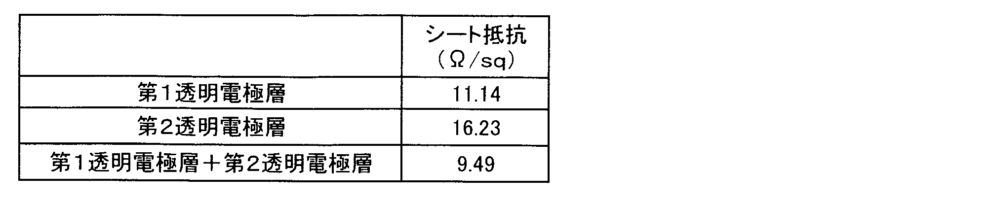
- Table 3 shows the sheet resistance of the first transparent electrode layer 22a and the second transparent electrode layer 22b formed under the film forming conditions shown in Table 1.
- the first transparent electrode layer 22a and the second transparent electrode layer 22b are formed on the substrate 20 as single layers having a film thickness of 400 nm and 500 nm, respectively, and the first transparent electrode layer 22a and the second transparent electrode layer 22b are formed.
- the sheet resistance when laminated at 400 nm and 100 nm, respectively, is shown. It can be seen that the first transparent electrode layer 22a has a lower sheet resistance than the second transparent electrode layer 22b. It can also be seen that the sheet resistance of the laminated film of the first transparent electrode layer 22a and the second transparent electrode layer 22b is also low. The higher the electrical conductivity, the lower the sheet resistance. The lower the sheet resistance, the smaller the loss when current flows.
- FIG. 5 shows the absorption coefficient of the first transparent electrode layer 22a and the second transparent electrode layer 22b formed under the film forming conditions shown in Table 1 with respect to the wavelength of light.
- the first transparent electrode layer 22a and the second transparent electrode layer 22b are formed on the substrate 20 as single layers having a film thickness of 400 nm and 500 nm, respectively, and the first transparent electrode layer 22a and the second transparent electrode layer 22b are formed.
- the absorption coefficient when laminated at 400 nm and 100 nm, respectively, is shown.
- the first transparent electrode layer 22a has a smaller absorption coefficient at all wavelengths measured than the second transparent electrode layer 22b.
- the laminated film of the first transparent electrode layer 22a and the second transparent electrode layer 22b also has a smaller absorption coefficient than the single-layer second transparent electrode layer 22b at all wavelengths, and in particular, a single layer in the wavelength region of 550 nm or more.
- the absorption coefficient is smaller than that of the first transparent electrode layer 22a. The smaller the light absorption rate, the smaller the absorption coefficient. The smaller the absorption coefficient, the smaller the absorption loss of light passing through the transparent electrode layer 22, and the power generation efficiency is improved.
- FIG. 6 shows the refractive index with respect to the wavelength of light of the first transparent electrode layer 22a and the second transparent electrode layer 22b formed under the film forming conditions shown in Table 1.
- the refractive index when the first transparent electrode layer 22a and the second transparent electrode layer 22b are formed on the substrate 20 as single layers having a film thickness of 400 nm and 500 nm, respectively, is shown.
- the refractive index increases when the density of the transparent electrode is increased.
- the film formation is performed under a high-density magnetic field, so that the first transparent electrode layer 22a is formed in a high-density state.
- the refractive index becomes small.
- the refractive index of the first transparent electrode layer 22a is smaller than that of the second transparent electrode layer 22b in a wavelength region of 440 nm or more, and at least in a wavelength region of 550 nm or more and 600 nm or less.
- the difference in refractive index from the substrate 20 such as a glass substrate is reduced, and reflection loss when light from the substrate 20 side is incident can be reduced.
- the refractive index of the first transparent electrode layer 22a is smaller than the refractive index of the second transparent electrode layer 22b, the substrate 20, the first transparent electrode layer 22a, the second transparent electrode layer 22b, a ⁇
- the refractive index gradually increases in the order of the Si unit 202. Thereby, the reflection loss before the light is incident on the a-Si unit 202 can be reduced, and the light can be effectively incident on the a-Si unit 202.
- the transparent electrode layer 22 has a laminated structure of the first transparent electrode layer 22a and the second transparent electrode layer 22b from the presence of the discontinuity of the impurity concentration in the film thickness direction of the transparent electrode layer 22. Can do.
- the concentration distribution of other impurities such as aluminum (Al) also shows discontinuities at the interface between the second transparent electrode layer 22b and the first transparent electrode layer 22a.
- the refractive index of each transparent electrode layer is reduced by adding Ga to the first transparent electrode layer 22a and the second transparent electrode layer 22b. For this reason, the refractive index difference with the substrate 20 such as a glass substrate becomes smaller, and the reflection loss when the light from the substrate 20 is incident can be reduced. Furthermore, the refractive index of the 1st transparent electrode layer 22a becomes still smaller than the 2nd transparent electrode layer 22b by making Ga density
- the refractive index gradually increases in the order of the substrate 20, the first transparent electrode layer 22a, the second transparent electrode layer 22b, and the a-Si unit 202 from the light incident side, and before light is incident on the a-Si unit 202.
- the reflection loss can be reduced, and light can be effectively incident on the a-Si unit 202.
- the addition of Si to the second transparent electrode layer 22b facilitates etching with a chemical solution, which will be described later, compared to the case where Si is not added, and the texture structure of the second transparent electrode layer 22b. Workability is improved.
- a texture structure is formed at least on the second transparent electrode layer 22b.
- a texture structure can be formed on the transparent electrode layer 22 by performing chemical etching.
- the first transparent electrode layer 22a and the second transparent electrode layer 22b are zinc oxide (ZnO)
- a texture structure can be formed by etching using 0.05% dilute hydrochloric acid.
- the transparent electrode 22 shown in FIG. 2 only the second transparent electrode layer 22b is etched, and a texture structure is formed in the second transparent electrode layer 22b so as not to reach the first transparent electrode layer 22a. That is, the level difference between the peak and valley of the texture provided on the transparent electrode 22 is smaller than the film thickness of the second transparent electrode layer 22b. With this structure, high electrical conductivity, low light absorption rate, and high light scattering effect can be obtained, and the performance of the photoelectric conversion device 200 can be improved.
- the transparent electrode 22 shown in FIG. 3 only the second transparent electrode layer 22b is etched, and a texture structure is formed in the second transparent electrode layer 22b so as to reach the first transparent electrode layer 22a. That is, the level difference between the crest and trough of the texture provided on the transparent electrode 22 is equal to the film thickness of the second transparent electrode layer 22b. In this structure, since the second transparent electrode layer 22b having a high light absorption rate is thinner, a higher light transmittance can be obtained.
- the first transparent electrode layer 22a is over-etched to form a texture structure on both the surface layer of the first transparent electrode layer 22a and the second transparent electrode layer 22b. That is, the level difference between the peak and valley of the texture provided on the transparent electrode 22 is larger than the film thickness of the second transparent electrode layer 22b. In this structure, the first transparent electrode layer 22a having a higher density than the second transparent electrode layer 22b is exposed on the surface. Further, because of the difference in etching rate between the first transparent electrode layer 22a and the second transparent electrode layer 22b, the texture angle ⁇ 1 formed on the surface of the first transparent electrode layer 22a is the texture formed on the second transparent electrode layer 22b.
- the angle ⁇ 2 is shallower than the angle ⁇ 2, the light scattering angle can be made different depending on the texture formed on the first transparent electrode layer 22a and the second transparent electrode layer 22b, thereby improving the light utilization rate. Can do. Further, by exposing the first transparent electrode layer 22a having a shallow angle, the film-forming surface of the power generation layer (a-Si unit 202) formed thereon becomes smooth, and the microcrystals formed thereon are formed. Crystal growth of the silicon layer ( ⁇ c-Si unit 204) can be promoted.
- the second transparent electrode layer 22b can also be formed by metal organic chemical vapor deposition (MOCVD method).
- MOCVD method metal organic chemical vapor deposition
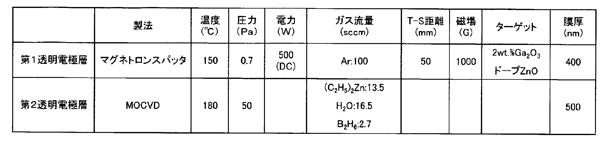
- the first transparent electrode layer 22a has a substrate 20 and a target facing each other with a surface interval of 50 mm in a vacuum chamber, and argon gas is flowed at 100 sccm and pressure 0.7 Pa at a substrate temperature of 150 ° C. Then, the film is introduced into a vacuum chamber and turned into plasma with a power of 500 W to form a film. At this time, the magnetic field is 1000 G.
- the second transparent electrode layer 22b are the raw material gas into the vacuum chamber at a substrate temperature of 180 °C (C 2 H 5) 2 Zn, H 2 O and B 2 H 6, respectively 13.5sccm, 16.5sccm and The film is introduced at a pressure of 50 Pa at 2.7 sccm.
- the second transparent electrode layer 22b is formed by the MOCVD method, the same characteristics of the transparent electrode 22 as described above can be obtained. Further, since the texture structure is naturally formed on the second transparent electrode layer 22b at the time of formation, the etching process may not be performed.
- the second transparent electrode layer 22b when the second transparent electrode layer 22b is formed by the MOCVD method, it may be a condition that boron is not doped.
- diborane B 2 H 6
- the source gas is contained in the vacuum chamber at a substrate temperature of 180 ° C.
- C 2 H 5 ) 2 Zn and H 2 O are introduced at 13.5 sccm and 16.5 sccm, respectively, so that the pressure is 50 Pa, and a film is formed.
- the transparent electrode 12 When the transparent electrode 12 is configured as a single layer as in the prior art, for example, as shown in Table 6, it is necessary to ensure conductivity by doping boron using diborane (B 2 H 6 ).
- the dopant concentration for generating carriers such as boron in the second transparent electrode layer 22b is lower than that in the first transparent electrode layer 22a. May be. Further, the second transparent electrode layer 22b may not be doped.
- Table 7 shows that when the first transparent electrode layer 22a and the second transparent electrode layer 22b are stacked on the substrate 20 with the film formation conditions shown in Table 5 at a film thickness of 400 nm and 1500 nm, respectively, The sheet resistance and the haze ratio when a single-layer transparent electrode having a structure is formed with a film thickness of 1500 nm are shown.
- the laminated structure of the first transparent electrode layer 22a and the second transparent electrode layer 22b in the present embodiment has a lower sheet resistance than the conventional single layer structure. Further, the laminated structure of the first transparent electrode layer 22a and the second transparent electrode layer 22b in the present embodiment has a higher haze ratio than the conventional single layer structure, that is, optical effects such as light confinement are also excellent. .
- the haze ratio is a physical quantity represented by scattering transmittance / total transmittance.
- FIG. 7 shows a case where the first transparent electrode layer 22a and the second transparent electrode layer 22b are stacked on the substrate 20 with the film formation conditions shown in Table 5 at a film thickness of 400 nm and 1500 nm, respectively.
- Table 5 The wavelength dependence of the total transmittance when a single-layer transparent electrode having a structure is formed with a film thickness of 1500 nm is shown.
- the laminated structure of the first transparent electrode layer 22a and the second transparent electrode layer 22b in the present embodiment is wider than the conventional single layer structure over a wide range except in the short wavelength region near the wavelength of 400 nm.
- the total transmittance was also high.
- the transparent electrode layer 22 is patterned into a strip shape.
- the transparent electrode layer 22 can be patterned into a strip shape using a YAG laser having a wavelength of 1064 nm, an energy density of 13 J / cm 2 , and a pulse frequency of 3 kHz.
- the a-Si unit 202 includes a silicon-containing gas such as silane (SiH 4 ), disilane (Si 2 H 6 ), dichlorosilane (SiH 2 Cl 2 ), a carbon-containing gas such as methane (CH 4 ), diborane (B 2 H 6 ) Plasma chemical vapor deposition in which a mixed gas obtained by mixing a p-type dopant-containing gas such as phosphine (PH 3 ) and a dilute gas such as phosphine (PH 3 ) and hydrogen (H 2 ) is formed into a plasma. It can be formed by the method (CVD method).
- a silicon-containing gas such as silane (SiH 4 ), disilane (Si 2 H 6 ), dichlorosilane (SiH 2 Cl 2 ), a carbon-containing gas such as methane (CH 4 ), diborane (B 2 H 6 )
- Plasma chemical vapor deposition in which a mixed gas obtained by mixing a
- an RF plasma CVD method of 13.56 MHz is preferably applied.
- the RF plasma CVD method can be a parallel plate type. It is good also as a structure which provided the gas shower hole for supplying the mixed gas of a raw material in the side which does not distribute
- Input power density of the plasma is preferably set to 5 mW / cm 2 or more 300 mW / cm 2 or less.
- the p-type layer is a single layer or a stacked structure such as an amorphous silicon layer, a microcrystalline silicon thin film, or a microcrystalline silicon carbide thin film having a thickness of 5 nm to 50 nm to which a p-type dopant (boron or the like) is added.
- the film quality of the p-type layer can be changed by adjusting the mixing ratio of the silicon-containing gas, the p-type dopant-containing gas and the dilution gas, the pressure, and the high frequency power for plasma generation.
- the i-type layer is an amorphous silicon film with a film thickness of 50 nm to 500 nm that is not added with a dopant formed on the p-type layer.
- the film quality of the i-type layer can be changed by adjusting the mixing ratio of the silicon-containing gas and the dilution gas, the pressure, and the high frequency power for plasma generation.
- the i-type layer becomes a power generation layer of the a-Si unit 202.
- the n-type layer is an n-type microcrystalline silicon layer (n-type ⁇ c-Si: H) having a thickness of 10 nm to 100 nm to which an n-type dopant (phosphorus or the like) formed on the i-type layer is added.
- the film quality of the n-type layer can be changed by adjusting the mixing ratio of the silicon-containing gas, the carbon-containing gas, the n-type dopant-containing gas and the dilution gas, the pressure, and the high-frequency power for plasma generation.
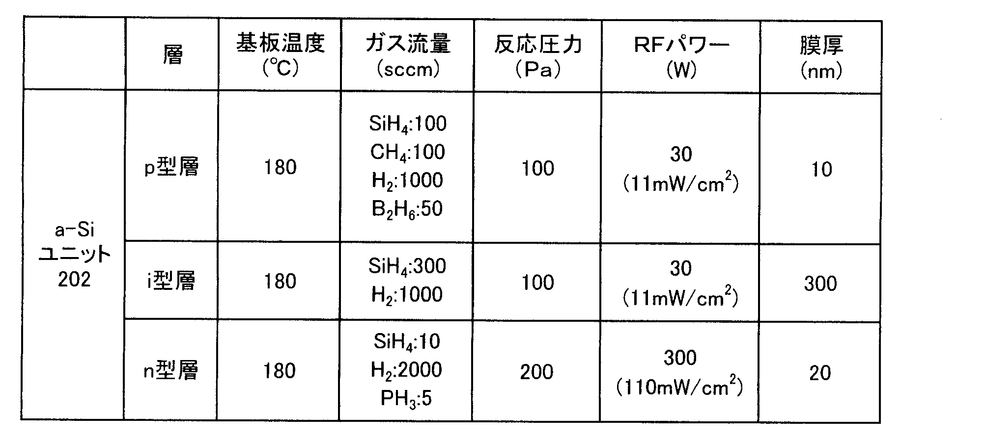
- the a-Si unit 202 is formed under the film formation conditions shown in Table 8.
- the intermediate layer 24 is formed on the a-Si unit 202.
- the intermediate layer 24 is preferably made of a transparent conductive oxide (TCO) such as zinc oxide (ZnO) or silicon oxide (SiOx). In particular, it is preferable to use zinc oxide (ZnO) or silicon oxide (SiOx) doped with magnesium (Mg).
- TCO transparent conductive oxide
- ZnO zinc oxide
- SiOx silicon oxide
- Mg magnesium
- the intermediate layer 24 can be formed by, for example, sputtering.
- the film thickness of the intermediate layer 24 is preferably in the range of 10 nm to 200 nm. The intermediate layer 24 may not be provided.
- the ⁇ c-Si unit 204 is formed by sequentially stacking a p-type layer, an i-type layer, and an n-type layer.
- the ⁇ c-Si unit 204 includes a silicon-containing gas such as silane (SiH 4 ), disilane (Si 2 H 6 ), dichlorosilane (SiH 2 Cl 2 ), a carbon-containing gas such as methane (CH 4 ), diborane (B 2 H 6 ) formed by a plasma CVD method in which a mixed gas obtained by mixing a p-type dopant-containing gas such as phosphine (PH 3 ) and a dilute gas such as phosphine (PH 3 ) and hydrogen (H 2 ) is formed into a plasma. can do.
- a silicon-containing gas such as silane (SiH 4 ), disilane (Si 2 H 6 ), dichlorosilane (SiH 2 Cl 2 )
- a carbon-containing gas such as
- the plasma CVD method it is preferable to apply, for example, a 13.56 MHz RF plasma CVD method as in the case of the a-Si unit 202.
- the RF plasma CVD method can be a parallel plate type. It is good also as a structure which provided the gas shower hole for supplying the mixed gas of a raw material in the side which does not distribute
- Input power density of the plasma is preferably set to 5 mW / cm 2 or more 300 mW / cm 2 or less.
- the p-type layer is a microcrystalline silicon layer ( ⁇ c-Si: H) to which a p-type dopant (boron or the like) having a thickness of 5 nm to 50 nm is added.
- a p-type dopant boron or the like
- the film quality of the p-type layer can be changed by adjusting the mixing ratio of the silicon-containing gas, the p-type dopant-containing gas and the dilution gas, the pressure, and the high frequency power for plasma generation.
- the i-type layer is a microcrystalline silicon layer ( ⁇ c-Si: H) formed on the p-type layer to which a dopant having a thickness of 0.5 ⁇ m to 5 ⁇ m is not added.
- the film quality of the i-type layer can be changed by adjusting the mixing ratio of the silicon-containing gas and the dilution gas, the pressure, and the high frequency power for plasma generation.
- the n-type layer is formed by stacking microcrystalline silicon layers (n-type ⁇ c-Si: H) to which an n-type dopant (phosphorus or the like) having a thickness of 5 nm to 50 nm is added.
- the film quality of the n-type layer can be changed by adjusting the mixing ratio of the silicon-containing gas, the n-type dopant-containing gas and the dilution gas, the pressure, and the high frequency power for plasma generation.
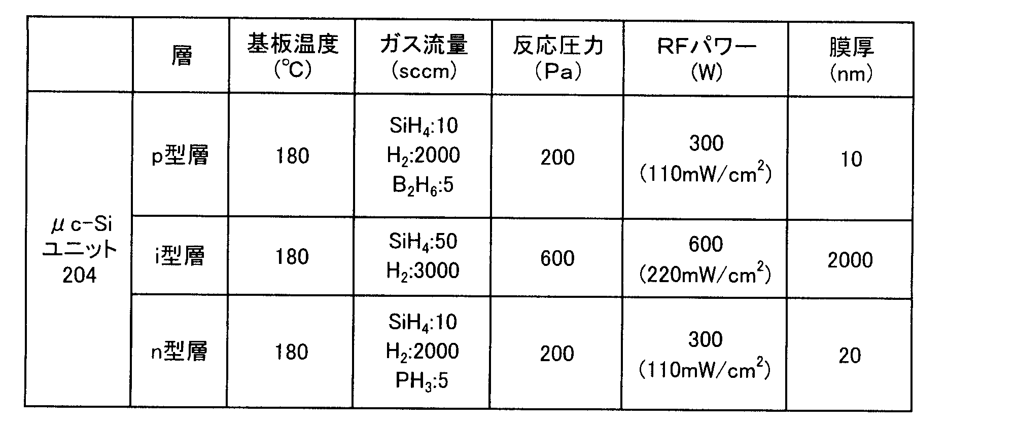
- the ⁇ c-Si unit 204 is formed under the film formation conditions shown in Table 9.
- the a-Si unit 202 and the ⁇ c-Si unit 204 are patterned into strips.
- a slit is formed by irradiating YAG laser at a position 50 ⁇ m lateral from the patterning position of the transparent electrode layer 22, and the a-Si unit 202 and the ⁇ c-Si unit 204 are patterned into strips.
- a YAG laser having an energy density of 0.7 J / cm 2 and a pulse frequency of 3 kHz is preferably used.
- a laminated structure of a transparent conductive oxide (TCO) and a reflective metal is formed on the ⁇ c-Si unit 204 as the first back electrode layer 26 and the second back electrode layer 28.
- a transparent conductive oxide (TCO) such as tin oxide (SnO 2 ), zinc oxide (ZnO), indium tin oxide (ITO), or the like is used.
- metals such as silver (Ag) and aluminum (Al), can be used.
- the transparent conductive oxide (TCO) can be formed by, for example, sputtering.
- the first back electrode layer 26 and the second back electrode layer 28 preferably have a thickness of about 1 ⁇ m in total. It is preferable that at least one of the first back electrode layer 26 and the second back electrode layer 28 is provided with unevenness for enhancing the light confinement effect.
- the first back electrode layer 26 and the second back electrode layer 28 are patterned into strips.
- a slit is formed by irradiating YAG laser at a position 50 ⁇ m lateral from the patterning position of the a-Si unit 202 and the ⁇ c-Si unit 204, and the first back electrode layer 26 and the second back electrode layer 28 are patterned into strips.
- a YAG laser having an energy density of 0.7 J / cm 2 and a pulse frequency of 4 kHz is preferably used.
- the back sheet 32 covers the surface of the second back electrode layer 28 with the filler 30.
- the filler 30 and the back sheet 32 can be made of a resin material such as EVA or polyimide. This can prevent moisture from entering the power generation layer of the photoelectric conversion device 200.
- the photoelectric conversion device 200 can be configured. It can be set as the favorable transparent electrode 22 with a high electrical conductivity, a low light absorption rate, and a high light-scattering effect, and the photoelectric conversion efficiency of the photoelectric conversion apparatus 200 can be improved.
- the first transparent electrode layer 22a having a high density and the second transparent electrode layer 22b having a low density are stacked, at least the second transparent electrode layer 22b having a low density is etched to be transparent. Since the texture can be easily formed on the electrode 22, the manufacturing cost of the photoelectric conversion device 200 can be reduced.
Landscapes
- Photovoltaic Devices (AREA)
Abstract
【課題】電気伝導率が高く、光の吸収率が低く、かつ高い光散乱効果を得ることができる透明電極を備えた光電変換装置を提供する。 【解決手段】透明電極層22として、基板20側に形成された第1透明電極層22aと、第1透明電極層22aより基板20から遠い位置に、第1透明電極層22aより密度が小さい第2透明電極層22bとを形成し、テクスチャ構造を設ける。
Description
本発明は、光電変換装置に関する。
太陽光を利用した発電システムとして、アモルファスや微結晶等の半導体薄膜を積層した光電変換装置が用いられている。
図11に、光電変換装置100の基本構成の断面模式図を示す。光電変換装置100は、ガラス等の透明基板10上に透明電極12、光電変換ユニット14及び裏面電極16を積層して形成される。透明基板10側から光を入射させることによって、光電変換装置100は光電変換ユニット14における光電変換により電力を発生させる。ここで、透明電極12は、一般的に、MOCVD法やスパッタリング法を用いて形成される(特許文献1参照)。
従来の透明電極12の形成方法は、高密度となる成膜条件下では高電気伝導率・低光吸収率の透明電極12が形成され、低密度となる成膜条件下では低電気伝導率・高光吸収率の透明電極12が形成される。
さらに光の利用率を高めるためには透明電極12の表面にテクスチャ構造を形成することが望ましいが、高電気伝導率・低光吸収率となる透明電極12は高密度であり、テクスチャ構造の加工が困難であるという問題がある。
この発明は、良好な特性(高電気伝導率、低光吸収率、高光散乱効果)を有する透明電極を提案し、これを備えた光電変換装置の性能の向上を図ることを目的とする。
本発明の1つの態様は、基板と、基板上に形成された透明電極層と、透明電極層上に形成された光電変換ユニットと、光電変換ユニット上に形成された裏面電極と、を備える光電変換装置であって、透明電極層は、光電変換ユニット側の表面にテクスチャ構造を有し、基板側に形成された第1透明電極層と、第1透明電極層より基板から遠い位置に、第1透明電極層より密度が小さい第2透明電極層と、を備える光電変換装置である。
本発明は、高電気伝導率、低光吸収率、高光散乱効果を有する透明電極を提案し、これを備えた光電変換装置の性能の向上を可能とする。
本実施の形態における光電変換装置200は、図1に示すように、基板20を光入射側として、光入射側から、透明電極層22、トップセルとして広いバンドギャップを有するアモルファスシリコン光電変換ユニット(a-Siユニット)202、中間層24、ボトムセルとしてa-Siユニット202よりバンドギャップの狭い微結晶シリコン光電変換ユニット(μc-Siユニット)204、第1裏面電極層26、第2裏面電極層28、充填材30及びバックシート32を積層した構造を有している。
本実施の形態では、発電層である光電変換ユニットとして、a-Siユニット202及びμc-Siユニット204を積層したタンデム型光電変換装置を例に説明を行うが、本発明の適用範囲はこれに限定されるものではなく、シングル型光電変換装置やさらに多層の光電変換装置であってもよい。
基板20は、例えば、ガラス基板、プラスチック基板等の少なくとも可視光波長領域において透過性を有する材料を適用することができる。
基板20上に透明電極層22が形成される。透明電極層22は、酸化錫(SnO2)、酸化亜鉛(ZnO)、インジウム錫酸化物(ITO)等に錫(Sn)、アンチモン(Sb)、フッ素(F)、アルミニウム(Al)等をドープした透明導電性酸化物(TCO)のうち少なくとも一種類又は複数種を組み合わせて用いることが好適である。特に、酸化亜鉛(ZnO)は、透光性が高く、抵抗率が低く、耐プラズマ特性にも優れているので好適である。
本実施の形態では透明電極層22は、図2~図4の拡大断面図に示すように、基板20上に第1透明電極層22a及び第2透明電極層22bを順に積層して構成される。第1透明電極層22aは、第2透明電極層22bよりも密度が高く、高い電気伝導率と低い光吸収率を有する電気伝導層である。また、第2透明電極層22bは、第1透明電極層22aよりも密度が低く、テクスチャ構造が形成される光散乱層である。透明電極層22をこうした積層構造とすることで、電気伝導率が高く、光の吸収率が低く、かつ、高い光散乱効果を有する透明電極とすることができる。
第1透明電極層22a及び第2透明電極層22bは、スパッタリング法で形成することができる。スパッタリング法では、真空槽内に設置した基板20に対向させて第1透明電極層22a及び第2透明電極層22bの材料となる元素を含むターゲットを配置し、プラズマ化したアルゴン等のスパッタ用ガスによりターゲットをスパッタリングすることによって基板20上に材料を堆積させて第1透明電極層22a及び第2透明電極層22bを形成する。
第1透明電極層22aは、第2透明電極層22bよりも高密度の磁場下におけるスパッタリング法で形成する。これにより、電気伝導層となる第1透明電極層22aは光散乱層となる第2透明電極層22bよりも緻密な層となり、第2透明電極層22bよりも高い電気伝導率及び低い光吸収率を示すことができる。一方、光散乱層となる第2透明電極層22bは電気伝導層となる第1透明電極層22aよりも疎な層となり、第1透明電極層22aよりも容易にテクスチャ構造に加工することができる。
例えば、第1透明電極層22a及び第2透明電極層22bは、表1に示すようにマグネトロンスパッタリング法により形成することが好適である。第1透明電極層22aは、真空槽内に基板20とターゲットを50mmの面間隔で対向配置し、基板温度150℃においてアルゴンガスを流量100sccm及び圧力0.7Paで真空槽に導入して500Wの電力によりプラズマ化して成膜する。このとき、磁場は1000Gとする。一方、第2透明電極層22bは、真空槽内に基板20とターゲットを50mmの面間隔で対向配置し、基板温度150℃においてアルゴンガスを流量100sccm及び圧力0.7Paで真空槽に導入して500Wの電力によりプラズマ化して成膜する。このとき、磁場は第1透明電極層22aを形成するときに比べて低い300Gとする。
透明電極層22の膜厚は、第1透明電極層22a及び第2透明電極層22bの膜厚を合わせて500nm以上5000nm以下の範囲とすることが好適である。例えば、第1透明電極層22aを400nmとし、第2透明電極層22bを100nmとする。

表2に、表1に示す成膜条件で形成した第1透明電極層22a及び第2透明電極層22bの密度をX線反射分析によって測定した結果を示す。ここでは、基板20上に第1透明電極層22a及び第2透明電極層22bをそれぞれ単層として形成した場合の密度を示す。より高密度の磁場下で形成された第1透明電極層22aは、第2透明電極層22bより膜の密度が高いことが分かる。
なお、第1透明電極層22a及び第2透明電極層22bを積層した場合であっても、エッチングやイオンミリング等によって第1透明電極層22a、第2透明電極層22bの表面を露出させた状態にすることでX線反射分析によるそれぞれの密度の測定が可能である。また、断面に対して電子エネルギー損失分光法(EELS:Electron Energy-Loss Spectroscopy)を適用しても第1透明電極層22a及び第2透明電極層22bの密度をそれぞれ測定することができる。

表3に、表1に示す成膜条件で形成した第1透明電極層22a及び第2透明電極層22bのシート抵抗を示す。ここでは、基板20上に第1透明電極層22a及び第2透明電極層22bをそれぞれ膜厚400nm及び500nmの単層として形成した場合、並びに第1透明電極層22a及び第2透明電極層22bをそれぞれ400nm及び100nmで積層した場合についてのシート抵抗を示す。第1透明電極層22aは、第2透明電極層22bよりもシート抵抗が低いことが分かる。また、第1透明電極層22aと第2透明電極層22bとの積層膜もシート抵抗が低くなることが分かる。電気伝導率が高いほどシート抵抗は低くなる。シート抵抗が低いほど電流が流れる際の損失が小さくなる。
また、図5に、表1に示す成膜条件で形成した第1透明電極層22a及び第2透明電極層22bの光の波長に対する吸収係数を示す。ここでは、基板20上に第1透明電極層22a及び第2透明電極層22bをそれぞれ膜厚400nm及び500nmの単層として形成した場合、並びに第1透明電極層22a及び第2透明電極層22bをそれぞれ400nm及び100nmで積層した場合についての吸収係数を示す。第1透明電極層22aは、第2透明電極層22bよりも測定した全波長において吸収係数が小さい。また、第1透明電極層22aと第2透明電極層22bとの積層膜も測定した全波長において単層の第2透明電極層22bよりも吸収係数が小さく、特に550nm以上の波長領域では単層の第1透明電極層22aよりも吸収係数が小さい。光吸収率が小さいほど吸収係数は小さくなる。吸収係数が小さいほど、透明電極層22を通過する光の吸収損失が小さくなり、発電効率が向上する。
また、図6に、表1に示す成膜条件で形成した第1透明電極層22a及び第2透明電極層22bの光の波長に対する屈折率を示す。ここでは、基板20上に第1透明電極層22a及び第2透明電極層22bをそれぞれ膜厚400nm及び500nmの単層として形成した場合についての屈折率を示す。従来の形成方法では、透明電極の密度を高くしようとすると屈折率が大きくなってしまうが、成膜を高密度な磁場下で行ったことで、高密度な状態で第1透明電極層22aの屈折率が小さくなる。特に、第1透明電極層22aは、440nm以上の波長領域、少なくとも550nm以上600nm以下の波長領域において第2透明電極層22bよりも屈折率が小さくなる。
第1透明電極層22aの屈折率を小さくしたことで、ガラス基板等の基板20との屈折率差が小さくなり、基板20側からの光が入射する際の反射損失を低減することができる。
また、第1透明電極層22aの屈折率が第2透明電極層22bの屈折率よりも小さいことで、光入射側から基板20、第1透明電極層22a、第2透明電極層22b、a-Siユニット202の順に徐々に屈折率が大きくなる構造となる。これにより、a-Siユニット202への光入射前の反射損失を低減でき、a-Siユニット202に効果的に光を入射させることができる。
また、図8~図10に、表1に示す成膜条件で積層した第1透明電極層22a及び第2透明電極層22bに含まれる亜鉛(Zn)、ガリウム(Ga)、シリコン(Si)及び銅(Cu)を二次イオン質量分析法(SIMS:Secondary Ion Mass Spectroscopy)で測定した結果を示す。ガリウム(Ga)、シリコン(Si)及び銅(Cu)のいずれにおいても、表面から深さ100nmにおいて含有濃度の不連続点が現れており、これが第2透明電極層22bと第1透明電極層22aとの界面であることを示している。このように、透明電極層22の膜厚方向における不純物濃度の不連続点の存在から、透明電極層22が第1透明電極層22a及び第2透明電極層22bの積層構造であることを知ることができる。なお、ここでは図示しないが、アルミニウム(Al)等の他の不純物の濃度分布も第2透明電極層22bと第1透明電極層22aとの界面において不連続点を示す。
ガリウム(Ga)の場合、第1透明電極層22aや第2透明電極層22bにGaを添加することで、各透明電極層の屈折率が小さくなる。このため、ガラス基板等の基板20との屈折率差がより小さくなり、基板20側からの光が入射する際の反射損失を低減することができる。さらに、第1透明電極層22aのGa濃度を第2透明電極層22bよりも多くすることで、第2透明電極層22bよりも第1透明電極層22aの屈折率がさらに小さくなる。これにより、第1透明電極層22aと基板20との間の屈折率差をさらに小さくすることが可能になり、上述の反射損失をより効果的に低減することができる。また、光入射側から基板20、第1透明電極層22a、第2透明電極層22b、a-Siユニット202の順に徐々に屈折率が大きくなる構造となり、a-Siユニット202への光入射前の反射損失を低減でき、a-Siユニット202に効果的に光を入射させることができる。
シリコン(Si)の場合、第2透明電極層22bにSiを添加することで、Siを添加しない場合に比べて、後述する薬液によるエッチングがし易くなり、第2透明電極層22bのテクスチャ構造の加工性が向上する。
また、少なくとも第2透明電極層22bにはテクスチャ構造を形成する。スパッタリング法により第1透明電極層22a及び第2透明電極層22bを形成した場合、化学的エッチングを施すことにより透明電極層22にテクスチャ構造を形成することができる。例えば、第1透明電極層22a及び第2透明電極層22bが酸化亜鉛(ZnO)である場合、0.05%希塩酸を用いたエッチングによりテクスチャ構造を形成することができる。
エッチング処理時間を調整することによって、図2~図4に示すように、透明電極層22に形成されるテクスチャ構造にバリエーションを設けることができる。
図2に示す透明電極22では、第2透明電極層22bのみエッチングし、第1透明電極層22aまで到達しないように第2透明電極層22bにテクスチャ構造を形成する。すなわち、透明電極22に設けられたテクスチャの山と谷との段差は第2透明電極層22bの膜厚よりも小さい。この構造によって、高い電気伝導度、低い光吸収率及び高い光散乱効果を得ることができ、光電変換装置200の性能を向上することができる。
図3に示す透明電極22では、第2透明電極層22bのみエッチングし、第1透明電極層22aまで到達するように第2透明電極層22bにテクスチャ構造を形成する。すなわち、透明電極22に設けられたテクスチャの山と谷との段差は第2透明電極層22bの膜厚と等しい。この構造では、光吸収率の高い第2透明電極層22bがより薄くなるので、より高い光透過率を得ることができる。
図4に示す透明電極22では、第1透明電極層22aまでオーバーエッチングし、第1透明電極層22aの表面層及び第2透明電極層22bの両方にテクスチャ構造を形成する。すなわち、透明電極22に設けられたテクスチャの山と谷との段差は第2透明電極層22bの膜厚よりも大きい。この構造では、第2透明電極層22bよりも高密度な第1透明電極層22aが表面に露出する。また、第1透明電極層22a及び第2透明電極層22bのエッチング速度の相違から、第1透明電極層22aの表面に形成されるテクスチャの角度θ1は第2透明電極層22bに形成されるテクスチャの角度θ2よりも浅くなるので、第1透明電極層22aと第2透明電極層22bとに形成されるそれぞれのテクスチャによって光の散乱角を異ならせることができ、光の利用率を向上させることができる。また、角度が浅くなる第1透明電極層22aを露出させることで、この上に形成される発電層(a-Siユニット202)の成膜面が平滑になり、その上に形成される微結晶シリコン層(μc-Siユニット204)の結晶成長を促進させることができる。
なお、第2透明電極層22bを有機金属気相成長法(MOCVD法)で形成することもできる。例えば、表4に示すように、第1透明電極層22aは、真空槽内に基板20とターゲットを50mmの面間隔で対向配置し、基板温度150℃においてアルゴンガスを流量100sccm及び圧力0.7Paで真空槽に導入して500Wの電力によりプラズマ化して成膜する。このとき、磁場は1000Gとする。一方、第2透明電極層22bは、基板温度180℃において真空槽内に原料ガスである(C2H5)2Zn,H2O及びB2H6をそれぞれ13.5sccm,16.5sccm及び2.7sccmで圧力50Paとなるように導入して成膜する。
このようにMOCVD法にて第2透明電極層22bを形成した場合も上記と同様の透明電極22の特性を得ることができる。また、形成時に第2透明電極層22bにテクスチャ構造が自然形成されるのでエッチング処理を行わなくてもよい。
また、第2透明電極層22bをMOCVD法にて形成する場合にボロンをドーピングしない条件としてもよい。例えば、表5に示すように、第2透明電極層22bを形成する際にジボラン(B2H6)を導入せず、基板温度180℃において真空槽内に原料ガスである(C2H5)2Zn及びH2Oをそれぞれ13.5sccm及び16.5sccmで圧力50Paとなるように導入して成膜する。
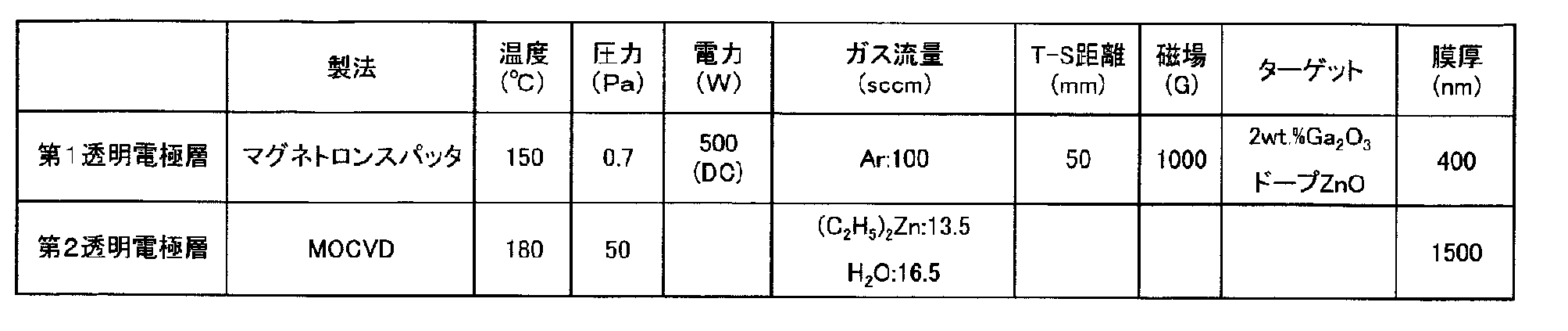
従来のように透明電極12を単層で構成する場合、例えば表6に示すように、ジボラン(B2H6)を用いてボロンをドーピングすることによって導電性を確保する必要がある。一方、本実施の形態では、第1透明電極層22aが高い導電性を有するので、第2透明電極層22bではボロン等のキャリアを発生させるためのドーパント濃度を第1透明電極層22aより低くしてもよい。さらに、第2透明電極層22bにはドーピングを行わなくてもよい。

表7に、表5に示す成膜条件で基板20上に第1透明電極層22a及び第2透明電極層22bをそれぞれ膜厚400nm及び1500nmで積層した場合、並びに表6の成膜条件で従来構造の単層の透明電極を膜厚1500nmで形成した場合についてのシート抵抗及びヘイズ率を示す。本実施の形態における第1透明電極層22aと第2透明電極層22bとの積層構造は従来の単層構造よりもシート抵抗が低かった。また、本実施の形態における第1透明電極層22aと第2透明電極層22bとの積層構造は従来の単層構造よりもヘイズ率が高く、すなわち光閉じ込め等の光学的な効果も優れている。なお、ヘイズ率は散乱透過率/全透過率で表される物理量である。

図7は、表5に示す成膜条件で基板20上に第1透明電極層22a及び第2透明電極層22bをそれぞれ膜厚400nm及び1500nmで積層した場合、並びに表6の成膜条件で従来構造の単層の透明電極を膜厚1500nmで形成した場合についての全透過率の波長依存性を示す。図7に示されるように、波長400nm付近の短波長領域以外では広範囲に亘って本実施の形態における第1透明電極層22aと第2透明電極層22bとの積層構造は従来の単層構造よりも全透過率が高かった。
タンデム型太陽電池100を複数のセルを直列に接続した構成とする場合、透明電極層22を短冊状にパターニングする。例えば、波長1064nm、エネルギー密度13J/cm2、パルス周波数3kHzのYAGレーザを用いて透明電極層22を短冊状にパターニングすることができる。
透明電極層22上に、p型層、i型層、n型層のシリコン系薄膜を順に積層してa-Siユニット202を形成する。a-Siユニット202は、シラン(SiH4)、ジシラン(Si2H6)、ジクロルシラン(SiH2Cl2)等のシリコン含有ガス、メタン(CH4)等の炭素含有ガス、ジボラン(B2H6)等のp型ドーパント含有ガス、フォスフィン(PH3)等のn型ドーパント含有ガス及び水素(H2)等の希釈ガスを混合した混合ガスをプラズマ化して成膜を行うプラズマ化学気相成長法(CVD法)により形成することができる。
プラズマCVD法は、例えば、13.56MHzのRFプラズマCVD法を適用することが好適である。RFプラズマCVD法は平行平板型とすることができる。平行平板型の電極のうち基板20を配しない側には原料の混合ガスを供給するためのガスシャワー孔を設けた構成としてもよい。プラズマの投入電力密度は、5mW/cm2以上300mW/cm2以下とすることが好ましい。
p型層は、p型ドーパント(ボロン等)を添加した膜厚5nm以上50nm以下のアモルファスシリコン層、微結晶シリコン薄膜、微結晶炭化シリコン薄膜等の単層又は積層構造とする。p型層の膜質は、シリコン含有ガス、p型ドーパント含有ガス及び希釈ガスの混合比、圧力及びプラズマ発生用高周波パワーを調整することによって変化させることができる。i型層は、p型層上に形成されたドーパントが添加されていない膜厚50nm以上500nm以下のアモルファスシリコン膜とする。i型層の膜質は、シリコン含有ガス及び希釈ガスの混合比、圧力及びプラズマ発生用高周波パワーを調整することによって変化させることができる。i型層は、a-Siユニット202の発電層となる。n型層は、i型層上に形成されたn型ドーパント(リン等)を添加した膜厚10nm以上100nm以下のn型微結晶シリコン層(n型μc-Si:H)とする。n型層の膜質は、シリコン含有ガス、炭素含有ガス、n型ドーパント含有ガス及び希釈ガスの混合比、圧力及びプラズマ発生用高周波パワーを調整することによって変化させることができる。例えば、a-Siユニット202は、表8に示す成膜条件で成膜する。
a-Siユニット202上に、中間層24を形成する。中間層24は、酸化亜鉛(ZnO)、酸化シリコン(SiOx)等の透明導電性酸化物(TCO)を用いることが好適である。特に、マグネシウム(Mg)がドープされた酸化亜鉛(ZnO)や酸化シリコン(SiOx)を用いることが好適である。中間層24は、例えば、スパッタリング等により形成することができる。中間層24の膜厚は10nm以上200nm以下の範囲とすることが好適である。なお、中間層24は、設けなくてもよい。
中間層24上に、p型層、i型層、n型層を順に積層したμc-Siユニット204を形成する。μc-Siユニット204は、シラン(SiH4)、ジシラン(Si2H6)、ジクロルシラン(SiH2Cl2)等のシリコン含有ガス、メタン(CH4)等の炭素含有ガス、ジボラン(B2H6)等のp型ドーパント含有ガス、フォスフィン(PH3)等のn型ドーパント含有ガス及び水素(H2)等の希釈ガスを混合した混合ガスをプラズマ化して成膜を行うプラズマCVD法により形成することができる。
プラズマCVD法は、a-Siユニット202と同様に、例えば、13.56MHzのRFプラズマCVD法を適用することが好適である。RFプラズマCVD法は平行平板型とすることができる。平行平板型の電極のうち基板20を配しない側には原料の混合ガスを供給するためのガスシャワー孔を設けた構成としてもよい。プラズマの投入電力密度は、5mW/cm2以上300mW/cm2以下とすることが好ましい。
p型層は、膜厚5nm以上50nm以下のp型ドーパント(ボロン等)が添加された微結晶シリコン層(μc-Si:H)とする。p型層の膜質は、シリコン含有ガス、p型ドーパント含有ガス及び希釈ガスの混合比、圧力及びプラズマ発生用高周波パワーを調整することによって変化させることができる。
i型層は、p型層上に形成された膜厚0.5μm以上5μm以下のドーパントが添加されていない微結晶シリコン層(μc-Si:H)である。i型層の膜質は、シリコン含有ガス及び希釈ガスの混合比、圧力及びプラズマ発生用高周波パワーを調整することによって変化させることができる。
n型層は、膜厚5nm以上50nm以下のn型ドーパント(リン等)が添加された微結晶シリコン層(n型μc-Si:H)を積層して構成される。n型層の膜質は、シリコン含有ガス、n型ドーパント含有ガス及び希釈ガスの混合比、圧力及びプラズマ発生用高周波パワーを調整することによって変化させることができる。例えば、μc-Siユニット204は、表9に示す成膜条件で成膜する。
複数のセルを直列接続する場合、a-Siユニット202及びμc-Siユニット204を短冊状にパターニングする。透明電極層22のパターンニング位置から50μm横の位置にYAGレーザを照射してスリットを形成し、a-Siユニット202及びμc-Siユニット204を短冊状にパターニングする。YAGレーザは、例えば、エネルギー密度0.7J/cm2、パルス周波数3kHzのものを用いることが好適である。
μc-Siユニット204上に、第1裏面電極層26、第2裏面電極層28として透明導電性酸化物(TCO)と反射性金属との積層構造を形成する。第1裏面電極層26としては、酸化錫(SnO2)、酸化亜鉛(ZnO)、インジウム錫酸化物(ITO)等の透明導電性酸化物(TCO)が用いられる。また、第2裏面電極層28としては、銀(Ag)、アルミニウム(Al)等の金属が使用できる。透明導電性酸化物(TCO)は、例えば、スパッタリング等により形成することができる。第1裏面電極層26及び第2裏面電極層28は、合わせて1μm程度の膜厚とすることが好適である。第1裏面電極層26及び第2裏面電極層28の少なくとも一方には、光閉じ込め効果を高めるための凹凸が設けることが好適である。
複数のセルを直列接続する場合、第1裏面電極層26及び第2裏面電極層28を短冊状にパターニングする。a-Siユニット202及びμc-Siユニット204のパターンニング位置から50μm横の位置にYAGレーザを照射してスリットを形成し、第1裏面電極層26、第2裏面電極層28を短冊状にパターニングする。YAGレーザは、エネルギー密度0.7J/cm2、パルス周波数4kHzのものを用いることが好適である。
さらに、充填材30によって第2裏面電極層28の表面をバックシート32で被う。充填材30及びバックシート32は、EVA、ポリイミド等の樹脂材料とすることができる。これによって、光電変換装置200の発電層への水分の侵入等を防ぐことができる。
以上のように、本発明の実施の形態における光電変換装置200を構成することができる。電気伝導率が高く、光の吸収率が低く、かつ高い光散乱効果を有する良好な透明電極22とすることができ、光電変換装置200の光電変換効率を向上させることができる。また、密度の高い第1透明電極層22aと密度の低い第2透明電極層22bとを積層した構造とすることによって、少なくとも密度の低い第2透明電極層22bに対してエッチングを行うことによって透明電極22にテクスチャを容易に形成することができるので、光電変換装置200の製造コストを低減することができる。
10 透明基板、12 透明電極、14 光電変換ユニット、16 裏面電極、20 基板、22 透明電極層、22a 第1透明電極層、22b 第2透明電極層、24 中間層、26 第1裏面電極層、28 第2裏面電極層、30 充填材、32 バックシート、100,200 光電変換装置、202 アモルファスシリコン光電変換ユニット、204 微結晶シリコン光電変換ユニット。
Claims (5)
- 基板と、前記基板上に形成された透明電極層と、前記透明電極層上に形成された光電変換ユニットと、前記光電変換ユニット上に形成された裏面電極と、を備える光電変換装置であって、
前記透明電極層は、前記光電変換ユニット側の表面にテクスチャ構造を有し、
前記基板側に形成された第1透明電極層と、
前記第1透明電極層より前記基板から遠い位置に、前記第1透明電極層より密度が小さい第2透明電極層と、
を備えることを特徴とする光電変換装置。 - 請求項1に記載の光電変換装置であって、
前記第1透明電極層は、波長550nm以上600nm以下の領域において前記第2透明電極層より屈折率が小さいことを特徴とする光電変換装置。 - 請求項1又は2に記載の光電変換装置であって
前記第1透明電極層には、前記第2透明電極層よりも高濃度のガリウム(Ga)が含まれることを特徴とする光電変換装置。 - 請求項1~3のいずれか1つに記載の光電変換装置であって、
前記テクスチャ構造は、段差が前記第2透明電極層の膜厚よりも小さいことを特徴とする光電変換装置。 - 請求項1~4のいずれか1つに記載の光電変換装置であって、
前記第2透明電極層は、前記第1透明電極層よりキャリアを発生させるためのドーパント濃度が低いことを特徴とする光電変換装置。
Priority Applications (2)
| Application Number | Priority Date | Filing Date | Title |
|---|---|---|---|
| CN2011800071957A CN102725856A (zh) | 2010-01-27 | 2011-01-14 | 光电转换装置 |
| US13/558,790 US20120299142A1 (en) | 2010-01-27 | 2012-07-26 | Photoelectric conversion device |
Applications Claiming Priority (4)
| Application Number | Priority Date | Filing Date | Title |
|---|---|---|---|
| JP2010015848 | 2010-01-27 | ||
| JP2010-015848 | 2010-01-27 | ||
| JP2011004845A JP4945686B2 (ja) | 2010-01-27 | 2011-01-13 | 光電変換装置 |
| JP2011-004845 | 2011-01-13 |
Related Child Applications (1)
| Application Number | Title | Priority Date | Filing Date |
|---|---|---|---|
| US13/558,790 Continuation US20120299142A1 (en) | 2010-01-27 | 2012-07-26 | Photoelectric conversion device |
Publications (1)
| Publication Number | Publication Date |
|---|---|
| WO2011093149A1 true WO2011093149A1 (ja) | 2011-08-04 |
Family
ID=44319141
Family Applications (1)
| Application Number | Title | Priority Date | Filing Date |
|---|---|---|---|
| PCT/JP2011/050561 Ceased WO2011093149A1 (ja) | 2010-01-27 | 2011-01-14 | 光電変換装置 |
Country Status (4)
| Country | Link |
|---|---|
| US (1) | US20120299142A1 (ja) |
| JP (1) | JP4945686B2 (ja) |
| CN (1) | CN102725856A (ja) |
| WO (1) | WO2011093149A1 (ja) |
Cited By (1)
| Publication number | Priority date | Publication date | Assignee | Title |
|---|---|---|---|---|
| WO2012157428A1 (ja) * | 2011-05-13 | 2012-11-22 | 三洋電機株式会社 | 光電変換装置 |
Families Citing this family (4)
| Publication number | Priority date | Publication date | Assignee | Title |
|---|---|---|---|---|
| KR101921236B1 (ko) | 2012-03-21 | 2019-02-13 | 엘지전자 주식회사 | 박막 태양 전지 및 그의 제조 방법 |
| JP6312060B2 (ja) * | 2012-10-31 | 2018-04-18 | パナソニックIpマネジメント株式会社 | 太陽電池 |
| CN111564112B (zh) * | 2020-06-09 | 2022-09-23 | 京东方科技集团股份有限公司 | 显示装置、显示面板及其制造方法 |
| CN113451429B (zh) * | 2021-06-30 | 2023-05-12 | 安徽华晟新能源科技有限公司 | 一种异质结太阳能电池及其制备方法 |
Citations (2)
| Publication number | Priority date | Publication date | Assignee | Title |
|---|---|---|---|---|
| JP2008277387A (ja) * | 2007-04-26 | 2008-11-13 | Kaneka Corp | 光電変換装置の製造方法 |
| JP2009140930A (ja) * | 2001-10-19 | 2009-06-25 | Asahi Glass Co Ltd | 透明導電性酸化物膜付き基体および光電変換素子 |
Family Cites Families (9)
| Publication number | Priority date | Publication date | Assignee | Title |
|---|---|---|---|---|
| JPH07131044A (ja) * | 1993-11-01 | 1995-05-19 | Asahi Glass Co Ltd | 透明導電性基板 |
| US6123824A (en) * | 1996-12-13 | 2000-09-26 | Canon Kabushiki Kaisha | Process for producing photo-electricity generating device |
| US6750394B2 (en) * | 2001-01-12 | 2004-06-15 | Sharp Kabushiki Kaisha | Thin-film solar cell and its manufacturing method |
| US6822158B2 (en) * | 2002-03-11 | 2004-11-23 | Sharp Kabushiki Kaisha | Thin-film solar cell and manufacture method therefor |
| US7615798B2 (en) * | 2004-03-29 | 2009-11-10 | Nichia Corporation | Semiconductor light emitting device having an electrode made of a conductive oxide |
| JP4301136B2 (ja) * | 2004-10-18 | 2009-07-22 | サンケン電気株式会社 | 半導体発光素子およびその製造方法 |
| JP2006120745A (ja) * | 2004-10-20 | 2006-05-11 | Mitsubishi Heavy Ind Ltd | 薄膜シリコン積層型太陽電池 |
| KR20080074086A (ko) * | 2005-11-17 | 2008-08-12 | 아사히 가라스 가부시키가이샤 | 태양 전지용 투명 도전성 기판 및 그 제조 방법 |
| US20090194157A1 (en) * | 2008-02-01 | 2009-08-06 | Guardian Industries Corp. | Front electrode having etched surface for use in photovoltaic device and method of making same |
-
2011
- 2011-01-13 JP JP2011004845A patent/JP4945686B2/ja not_active Expired - Fee Related
- 2011-01-14 CN CN2011800071957A patent/CN102725856A/zh active Pending
- 2011-01-14 WO PCT/JP2011/050561 patent/WO2011093149A1/ja not_active Ceased
-
2012
- 2012-07-26 US US13/558,790 patent/US20120299142A1/en not_active Abandoned
Patent Citations (2)
| Publication number | Priority date | Publication date | Assignee | Title |
|---|---|---|---|---|
| JP2009140930A (ja) * | 2001-10-19 | 2009-06-25 | Asahi Glass Co Ltd | 透明導電性酸化物膜付き基体および光電変換素子 |
| JP2008277387A (ja) * | 2007-04-26 | 2008-11-13 | Kaneka Corp | 光電変換装置の製造方法 |
Cited By (1)
| Publication number | Priority date | Publication date | Assignee | Title |
|---|---|---|---|---|
| WO2012157428A1 (ja) * | 2011-05-13 | 2012-11-22 | 三洋電機株式会社 | 光電変換装置 |
Also Published As
| Publication number | Publication date |
|---|---|
| JP4945686B2 (ja) | 2012-06-06 |
| US20120299142A1 (en) | 2012-11-29 |
| JP2011176284A (ja) | 2011-09-08 |
| CN102725856A (zh) | 2012-10-10 |
Similar Documents
| Publication | Publication Date | Title |
|---|---|---|
| JP4940290B2 (ja) | 光電変換装置及びその製造方法 | |
| JP4902779B2 (ja) | 光電変換装置及びその製造方法 | |
| JP4767365B2 (ja) | 薄膜太陽電池及びその製造方法 | |
| JP4945686B2 (ja) | 光電変換装置 | |
| JP2010283161A (ja) | 太陽電池及びその製造方法 | |
| JP4902767B2 (ja) | 光電変換装置 | |
| JP4940327B2 (ja) | 光電変換装置 | |
| US20110056560A1 (en) | Solar cell module and manufacturing method thereof | |
| WO2012157405A1 (ja) | 光電変換装置 | |
| WO2011136167A1 (ja) | 光電変換装置 | |
| JP5373045B2 (ja) | 光電変換装置 | |
| WO2011105166A1 (ja) | 光電変換モジュール及びその製造方法 | |
| JP2010283162A (ja) | 太陽電池及びその製造方法 | |
| WO2012157428A1 (ja) | 光電変換装置 | |
| JP4642126B2 (ja) | 積層型光起電力素子および積層型光起電力素子の製造方法 | |
| JP2011216586A (ja) | 積層型光電変換装置および積層型光電変換装置の製造方法 | |
| WO2012081656A1 (ja) | 光電変換装置及びその製造方法 | |
| US20100330266A1 (en) | Method of manufacturing solar battery | |
| WO2013080803A1 (ja) | 光起電力装置 | |
| JP2013098249A (ja) | 光起電力装置及びその製造方法 | |
| JP2013026602A (ja) | 光電変換装置 | |
| JP2010283159A (ja) | 太陽電池及びその製造方法 | |
| WO2013065538A1 (ja) | 光電変換装置 | |
| JP2013115339A (ja) | 光起電力装置 | |
| JP2013065751A (ja) | 太陽電池 |
Legal Events
| Date | Code | Title | Description |
|---|---|---|---|
| WWE | Wipo information: entry into national phase |
Ref document number: 201180007195.7 Country of ref document: CN |
|
| 121 | Ep: the epo has been informed by wipo that ep was designated in this application |
Ref document number: 11736864 Country of ref document: EP Kind code of ref document: A1 |
|
| NENP | Non-entry into the national phase |
Ref country code: DE |
|
| 122 | Ep: pct application non-entry in european phase |
Ref document number: 11736864 Country of ref document: EP Kind code of ref document: A1 |