WO2011077950A1 - コンデンサ素子製造用反応容器及びコンデンサ素子の製造方法 - Google Patents
コンデンサ素子製造用反応容器及びコンデンサ素子の製造方法 Download PDFInfo
- Publication number
- WO2011077950A1 WO2011077950A1 PCT/JP2010/071990 JP2010071990W WO2011077950A1 WO 2011077950 A1 WO2011077950 A1 WO 2011077950A1 JP 2010071990 W JP2010071990 W JP 2010071990W WO 2011077950 A1 WO2011077950 A1 WO 2011077950A1
- Authority
- WO
- WIPO (PCT)
- Prior art keywords
- capacitor element
- container
- partition frame
- conductor
- semiconductor layer
- Prior art date
- Legal status (The legal status is an assumption and is not a legal conclusion. Google has not performed a legal analysis and makes no representation as to the accuracy of the status listed.)
- Ceased
Links
Images


Classifications
-
- H—ELECTRICITY
- H01—ELECTRIC ELEMENTS
- H01G—CAPACITORS; CAPACITORS, RECTIFIERS, DETECTORS, SWITCHING DEVICES, LIGHT-SENSITIVE OR TEMPERATURE-SENSITIVE DEVICES OF THE ELECTROLYTIC TYPE
- H01G9/00—Electrolytic capacitors, rectifiers, detectors, switching devices, light-sensitive or temperature-sensitive devices; Processes of their manufacture
-
- H—ELECTRICITY
- H01—ELECTRIC ELEMENTS
- H01G—CAPACITORS; CAPACITORS, RECTIFIERS, DETECTORS, SWITCHING DEVICES, LIGHT-SENSITIVE OR TEMPERATURE-SENSITIVE DEVICES OF THE ELECTROLYTIC TYPE
- H01G9/00—Electrolytic capacitors, rectifiers, detectors, switching devices, light-sensitive or temperature-sensitive devices; Processes of their manufacture
- H01G9/0029—Processes of manufacture
- H01G9/0032—Processes of manufacture formation of the dielectric layer
-
- H—ELECTRICITY
- H01—ELECTRIC ELEMENTS
- H01G—CAPACITORS; CAPACITORS, RECTIFIERS, DETECTORS, SWITCHING DEVICES, LIGHT-SENSITIVE OR TEMPERATURE-SENSITIVE DEVICES OF THE ELECTROLYTIC TYPE
- H01G13/00—Apparatus specially adapted for manufacturing capacitors; Processes specially adapted for manufacturing capacitors not provided for in groups H01G4/00 - H01G11/00
-
- Y—GENERAL TAGGING OF NEW TECHNOLOGICAL DEVELOPMENTS; GENERAL TAGGING OF CROSS-SECTIONAL TECHNOLOGIES SPANNING OVER SEVERAL SECTIONS OF THE IPC; TECHNICAL SUBJECTS COVERED BY FORMER USPC CROSS-REFERENCE ART COLLECTIONS [XRACs] AND DIGESTS
- Y10—TECHNICAL SUBJECTS COVERED BY FORMER USPC
- Y10T—TECHNICAL SUBJECTS COVERED BY FORMER US CLASSIFICATION
- Y10T29/00—Metal working
- Y10T29/43—Electric condenser making
Definitions
- the present invention relates to a reaction container for manufacturing a capacitor element and manufacturing of a capacitor element that can stably form a uniform dielectric layer or a uniform semiconductor layer with respect to a plurality of conductors while maintaining the formation range constant. Regarding the method.
- Capacitors used in CPU (central processing unit) circuits used in personal computers and the like have high capacity and low ESR (in order to suppress voltage fluctuations and to reduce heat generation when passing through high ripple). Equivalent series resistance).
- An aluminum solid electrolytic capacitor and a tantalum solid electrolytic capacitor are known as capacitors used in the CPU circuit.
- these solid electrolytic capacitors one electrode (conductor) made of a sintered body obtained by sintering an aluminum foil having fine pores in the surface layer or tantalum powder having minute pores inside, and the electrode There is known one composed of a dielectric layer formed on the surface and the other electrode (usually a semiconductor layer) formed on the dielectric layer.
- Patent Document 1 Japanese Patent No. 1868722
- Patent Document 2 Japanese Patent No. 1985056
- Patent Document 3 Japanese Patent No. 2054506
- a method of forming by the energization method described in 3 is known. In either case, a conductor provided with a dielectric layer on the surface is immersed in a semiconductor layer forming solution, and a voltage is applied between the cathode prepared in the semiconductor layer forming solution with the conductor side serving as an anode (current flows). This is a method for forming a semiconductor layer.
- Patent Document 4 describes a method of forming a semiconductor layer by flowing a current obtained by superimposing a DC bias current on an alternating current through a conductor provided with a dielectric layer.
- Patent Document 5 discloses that a conductor is brought into contact with a chemical polymerization layer provided on a dielectric layer, and a semiconductor layer is formed on the chemical polymerization layer by electrolytic polymerization using the conductor as an anode. How to do is described.
- Patent Documents 4 and 5 have the following problems when a semiconductor layer is formed on a plurality of conductors at the same time. That is, the method described in Patent Document 4 has a problem that a semiconductor layer is formed also on the cathode side, and the formation state of the semiconductor layer changes as the energization time elapses, and current is uniformly distributed to a plurality of conductors. It was difficult to shed. Further, in the method described in Patent Document 5, since a conductor provided outside is energized as an anode, it is difficult to form a uniform semiconductor layer inside each conductor. With a conductor having a small internal pore and a large shape, it has been particularly difficult to form a uniform semiconductor layer.
- each conductor is not necessarily homogeneous, and the formation speed of the semiconductor may vary depending on the conductor, so the semiconductor layers are formed on many conductors at the same time. In this case, the value of the current flowing through each conductor is not constant, and there are cases where it is difficult to fabricate a capacitor having a stable capacity due to uneven formation of the semiconductor layer of the fabricated capacitor.
- Japanese Patent No. 1868722 Japanese Patent No. 1985056
- Japanese Patent No. 2054506 Japanese Patent Laid-Open No. 3-22516 JP-A-3-163816 WO2006 / 028286 Pamphlet Japanese Patent No. 40498804
- a minute hole is provided between adjacent individual chambers so that the liquid level of each individual chamber (compartment) can be adjusted to the same height.
- a potential difference between elements (between conductors) may be large particularly in the initial stage, and a current that cannot be ignored from the viewpoint of uniformizing the dielectric layer.
- the present invention has been made in view of such a technical background, and is capable of performing an electrolytic reaction such as anodization or electropolymerization at a predetermined current value for each conductor disposed in each individual chamber (compartment).
- the liquid level in each individual chamber (compartment) of the container can be adjusted to the same height (same level), and the uniformity of the electrolyte in each individual chamber can also be adjusted.
- an object of the present invention is to provide a capacitor element manufacturing reaction vessel and a capacitor element manufacturing method capable of stably forming a uniform dielectric layer and a uniform semiconductor layer while maintaining the formation range constant.
- the present invention provides the following means.
- a container for containing an electrolyte solution A partition frame capable of dividing the inside of the container into a plurality of individual chambers; Cathode bodies individually arranged in the individual chambers, A reaction vessel for manufacturing a capacitor element, characterized in that a passage enabling movement of an electrolyte is provided between the individual chamber and at least one of the individual chambers adjacent to the individual chamber.
- the partition frame includes a lower partition frame projecting upward from the bottom surface of the container, and an upper partition frame capable of contacting the upper surface of the lower partition frame in a liquid-tight state.
- the upper partition frame can be moved up and down,
- the inside of the container can be partitioned into a plurality of individual chambers by overlapping the upper partition frame on the upper surface of the lower partition frame, and the upper partition frame is separated from the lower partition frame.
- the reaction container for manufacturing a capacitor element according to the preceding item 1, wherein the passage can be formed between the two partition frames.
- a first abutting plate portion is provided at an upper end of the partition wall of the lower partition frame, and an upper surface of the first abutting plate portion is formed as a smooth surface, and an upper surface of the first abutting plate portion.
- the width of is set larger than the thickness of the partition wall of the lower partition frame
- a second contact plate portion is provided at the lower end of the partition wall of the upper partition frame, the lower surface of the second contact plate portion is formed as a smooth surface
- the width of the lower surface of the second contact plate portion is: It is set larger than the thickness of the partition wall of the upper partition frame, The upper partition frame on the upper surface of the lower partition frame so that the lower surface of the second contact plate portion of the upper partition frame contacts the upper surface of the first contact plate portion of the lower partition frame.
- reaction container for manufacturing a capacitor element according to any one of items 1 to 3, wherein a liquid passage space is provided inside a constituent wall of the container.
- reaction container for manufacturing a capacitor element according to any one of the above items 1 to 4, further comprising a circuit board having a power source capable of limiting voltage and current electrically connected to the cathode body.
- the above-mentioned items 1 to 7 are used for forming a dielectric layer on the surface of the anode body by anodizing by immersing a plurality of conductors individually in the chemical conversion solution in each chamber of the container.
- a conductor having a dielectric layer provided on the surface thereof is individually immersed, and the conductor is put in a state where the passage is closed.
- a liquid level adjustment step of adjusting a liquid level of the semiconductor layer forming solution by opening a passage of the reaction vessel.
- a dielectric layer forming step of forming a dielectric layer on the surface of the conductor A first liquid level adjustment step of opening the passage of the reaction vessel and adjusting the liquid level of the chemical conversion treatment liquid;
- the conductor obtained through the dielectric layer forming step and provided with a dielectric layer on the surface is individually immersed in the semiconductor layer forming solution in each individual chamber of the capacitor element manufacturing reaction vessel,
- Semiconductor layer formation for forming a semiconductor layer on the surface of the dielectric layer on the surface of the conductor by energizing with the conductor as an anode and the cathode of the reaction vessel as a cathode with the passage closed Process And a second liquid level adjusting step of adjusting a liquid level of the semiconductor layer forming solution by opening a passage of the reaction vessel.
- Electrode terminals are electrically connected to the conductor and the semiconductor layer of the capacitor element obtained by the manufacturing method according to any one of items 10 to 13, respectively, and a part of the electrode terminals is left and sealed. Capacitor manufacturing method to stop.
- each conductor (anode body) arranged in each of the individual chambers (sections) has a predetermined constant current value.
- Electrolytic reaction such as anodic oxidation and electropolymerization can be performed in a precisely controlled state, and uniform dielectric layers and uniform semiconductor layers can be formed for a plurality of conductors (anode bodies).
- each individual chamber can be opened by opening the passage.
- the liquid level in (compartments) can be adjusted to the same height (same level), the dielectric layer formation range and the semiconductor layer formation range in each conductor (anode body) can be kept constant, and the passage By opening it, it is possible to adjust the uniformity of the electrolyte in each chamber (for example, the uniformity of the concentration, etc.), so that a uniform capacitor element can be manufactured.
- the partition frame includes a lower partition frame projecting upward from the bottom surface of the container, and an upper side capable of contacting the upper surface of the lower partition frame in a liquid-tight state.
- the upper partition frame is vertically movable. Therefore, the upper partition frame is overlaid on the upper surface of the lower partition frame, and the passage is closed, and a plurality of interiors of the container are formed. Since it can be divided into individual chambers, an electrolytic reaction such as anodic oxidation or electrolytic polymerization can be performed in a state where each conductor (anode body) arranged in each individual chamber (section) is precisely controlled to a predetermined constant current value. it can.
- each individual chamber (compartment)
- the liquid surface can be adjusted to the same height (same level), and the electrolyte solution in each individual chamber can be adjusted to be uniform (for example, the concentration is uniform).
- the strength of the container can be further increased (can be reinforced).
- the area of the upper surface (contact surface) of the first contact plate at the upper end of the partition wall of the lower partition frame and the second contact plate at the lower end of the partition wall of the upper partition frame Since the area of the lower surface (abutment surface) can be ensured to be large, the contact area between the abutment surfaces is increased, and a sufficiently liquid-tight state is obtained when the upper partition frame is overlaid on the upper surface of the lower partition frame Can be secured.
- the capacitor element manufacturing reaction vessel further includes a circuit board having a power source capable of limiting the voltage and current electrically connected to the cathode body.
- circuit board is arranged on the bottom surface side of the container, it is possible to save space as a reaction container device and to increase the strength of the container, particularly the strength of the bottom surface of the container. (Can be reinforced).
- the components (particularly semiconductor components) constituting the power supply are thermally coupled to the temperature-controlled container, so that the temperature of the components constituting the power supply can be controlled to some extent.
- the operating state of the power source can be stabilized, and a more uniform dielectric layer and a more uniform semiconductor layer can be formed.
- the invention [8] provides a reaction vessel capable of forming a uniform dielectric layer for a plurality of conductors (anode bodies).
- reaction vessel capable of forming a uniform semiconductor layer on a plurality of conductors (anode bodies) having a dielectric layer formed on the surface thereof is provided.
- each conductor (anode body) disposed in each individual chamber (compartment) of the reaction vessel can be subjected to an anodic oxidation reaction or the like in a state of being precisely controlled to a predetermined constant current value,
- a uniform dielectric layer can be formed for a plurality of conductors (anode bodies), and the liquid level in each individual chamber (compartment) can be adjusted to the same height by opening the passage of the compartment frame. Since the dielectric layer forming range in the conductor (anode body) can be kept constant, a large number of uniform capacitor elements can be manufactured.
- an electropolymerization reaction or the like can be performed in a state where each conductor (anode body) disposed in each individual chamber (compartment) of the reaction vessel is precisely controlled to a predetermined constant current value, A uniform semiconductor layer can be formed for a plurality of conductors (anode bodies), and the liquid level in each individual chamber (partition) can be adjusted to the same height by opening the passage of the partition frame. Since the semiconductor layer formation range in the body (anode body) can be kept constant, a large number of uniform capacitor elements can be manufactured.
- an electrolytic reaction such as anodic oxidation or electrolytic polymerization is performed in a state where each conductor (anode body) disposed in each individual chamber (compartment) of the reaction vessel is precisely controlled to a predetermined constant current value.
- a uniform dielectric layer and a uniform semiconductor layer can be formed on a plurality of conductors (anode bodies), and the liquid in each individual chamber (partition) can be formed by opening a passage of the partition frame. Since the surface can be adjusted to the same height (same level) and the dielectric layer formation range and semiconductor layer formation range of each conductor (anode body) can be kept constant, a large number of uniform capacitor elements can be manufactured. Can do.
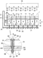
- FIG. 3 is a sectional view taken along line XX in FIG. 2 (shown together with a capacitor element manufacturing jig). It is a top view which shows a circuit board. It is a bottom view which shows a circuit board. It is a partial cross section figure which shows the arrangement
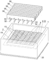
- This capacitor element manufacturing reaction container 1 includes a container 2, a partition frame 3, a cathode body 6, and a power source 7 capable of limiting voltage and current.
- the container 2 is a container for accommodating an electrolytic solution (chemical conversion solution, semiconductor layer forming solution, etc.) inside.
- the container 2 has a substantially rectangular parallelepiped shape with an open upper surface, and is formed of an insulating material such as resin (acrylic resin or the like) (see FIG. 1).
- the container 2 has a jacket structure. That is, as shown in FIG. 3, the container 2 is provided with a liquid passage space 21 that communicates the inside of the four side walls and the inside of the bottom wall.
- a temperature-controlled liquid for example, hot water
- the temperature of the electrolyte (chemical conversion solution, semiconductor layer forming solution, etc.) accommodated in the container 2 is controlled with high accuracy. be able to.
- the partition frame 3 includes a lower partition frame 4 that protrudes upward from the bottom wall of the container 2, and an upper partition that can abut on the upper surface of the lower partition frame 4 in a liquid-tight state.
- Frame body 5 (see FIG. 3).
- the lower partition frame 4 and the upper partition frame 5 are both made of an insulating material such as resin (acrylic resin or the like).
- the upper partition frame 5 is movable up and down by driving means (not shown).
- the lower partition frame 4 and the bottom wall of the container 2 are joined to each other in a liquid-tight state so that the electrolyte solution 19 does not leak.
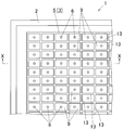
- the lower partition frame 4 is configured by connecting a vertical partition wall 11 and a horizontal partition wall 11 in an orthogonal state so as to form a plurality of substantially grid-like individual chambers 9 in plan view (FIG. 1 to 3).
- a first contact plate 12 is connected to the upper end of the partition wall 11 of the lower partition frame 4 (see FIG. 3).
- the upper surface of the first contact plate portion 12 is formed as a smooth surface.
- the width (W 1 ) of the upper surface of the first contact plate portion 12 is larger than the thickness (T 1 ) of the partition wall 11 of the lower partition frame 4 (see FIG. 3).
- the upper partition frame 5 is configured by connecting a vertical partition wall 13 and a horizontal partition wall 13 in an orthogonal state so as to form a plurality of substantially grid-like individual chambers 9 in plan view (FIG. 1). To 3). The number, arrangement, and arrangement of the individual chambers 9 in the upper partition frame 5 in the plan view are the same as the arrangement, size, and arrangement of the individual chambers 9 in the lower division frame 4 ( 1 to 3).
- a second contact plate portion 14 is connected to the lower end of the partition wall 13 of the upper partition frame 5 (see FIG. 3). The lower surface of the second contact plate portion 14 is formed as a smooth surface. The width (W 2 ) of the lower surface of the second contact plate portion 14 is larger than the thickness (T 2 ) of the partition wall 13 of the upper partition frame 5 (see FIG. 3).
- the plurality of individual chambers 9 are arranged in a substantially grid pattern.
- the present invention is not particularly limited to such a configuration, and for example, a honeycomb arrangement may be adopted.
- the lower partition frame 4 is arranged so that the lower surface of the second contact plate portion 14 of the upper partition frame 5 is brought into contact with the upper surface of the first contact plate portion 12 of the lower partition frame 4.
- the inside of the container 2 can be divided into a plurality of individual chambers 9 in a liquid-tight state (in a state where there is no liquid leakage between the individual chambers) (see FIG. 6). ).
- the lower partition frame A passage 8 can be formed between the body 4 and the upper partition frame 5 (between the first contact plate 12 and the second contact plate 14) (see FIG. 3).
- the partition frame 3 is in liquid-tight contact with the lower partition frame 4 projecting from the bottom surface of the container 2 and the upper surface of the lower partition frame 4. Since the upper partition frame 5 is configured to be movable up and down, the electrolyte solution can be moved between the plurality of individual chambers 9 when opened and closed.
- the container 2 is provided with an openable and closable passage 8 that enables the inside of the container 2 to be divided into a plurality of individual chambers 9 in a liquid-tight state. That is, by overlapping the upper partition frame 5 on the upper surface of the lower partition frame 4, the passage 8 is closed (see FIG. 6), and the upper partition frame 5 is moved from the lower partition frame 4.
- path 8 is open
- a pair of upper and lower walls forming the liquid passage space 21 in the bottom wall of the container 2 are formed with through holes 36 having a circular shape in plan view at positions corresponding to each other in the vertical direction (see FIG. 3).
- a cylindrical pipe 31 is inserted and arranged in an adapted state from the through hole 36 in the upper wall to the through hole 36 in the lower wall. Further, a gap between the inner peripheral surface of the through hole 36 and the outer peripheral surface of the end portion of the pipe 31 is made of silicone resin or the like so that the temperature adjusting liquid flowing in the liquid passage space 21 does not leak outside.
- the sealing resin 32 is used (see FIG. 3).
- a circuit board 22 is disposed on the bottom side of the container 2. That is, the circuit board 22 is fixed to the lower surface of the bottom wall of the container 2 via the spacer 35 (see FIG. 3).
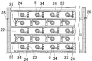
- an electric circuit having a pair of electric connection terminals 25 and 26 is formed on the upper surface of the circuit board 22.
- one terminal 25 is provided at one end of the circuit board 22, and the other terminal 26 is provided at the other end of the circuit board 22.
- One electrical connection terminal is a current limiting terminal 25, and the other electrical connection terminal is a voltage limiting terminal 26.
- An insulating substrate is used as the circuit board 22.
- the material of the insulating substrate is not particularly limited, and examples thereof include glass epoxy resin, imide resin, and ceramics.
- the electric circuit is formed of copper foil or the like.
- a resistor 23 and a transistor 24 are attached to the upper surface of the circuit board 22 (see FIGS. 3 and 4). As shown in the electrical circuit diagram of FIG. 7, one end of the resistor 23 is connected to the current limiting terminal 25, the other end of the resistor 23 is connected to the emitter of the transistor 24, and the collector of the transistor 24 is connected.
- the cathode body 6 is connected to the transistor 24, and the base of the transistor 24 is connected to the voltage limiting terminal 26.
- the cathode body 6 is connected to a power source 7 capable of limiting the voltage and current as shown in FIGS.
- the power source 7 capable of limiting the voltage and current of the circuit board 22 is preferably a constant current source as shown in FIG. 7, but is not limited thereto.
- a plurality of through holes 27 penetrating in the vertical direction are formed in the circuit board 22 (see FIG. 3). These through-holes 27 are provided in the same arrangement as the through-holes 36 in the bottom wall of the container 2 (the vertical arrangement interval is the same and the horizontal arrangement interval is the same).
- the shaft portion 6B of the cathode body 6 made of a bolt is inserted into the through hole 36 in the bottom wall of the container 2 from above, and further inserted into the through hole 27 of the circuit board 22,
- the first nut 33 is screwed and fastened to the tip end portion of the bolt shaft portion 6B protruding downward from the through hole 27 of the circuit board 22, whereby the circuit board 22 is fixed to the bottom surface side of the container 2.
- the head 6A of the bolt protrudes from the bottom surface of each individual chamber 9 to constitute the cathode body 6 (see FIGS. 3 and 5). In this way, the cathode bodies 6 are individually arranged in the individual chambers 9 (see FIGS. 2 and 3).
- the second nut 34 is screwed to the shaft portion 6B of the cathode body 6 in such a manner that the second nut 34 is in electrical contact with the electric circuit on the upper surface of the circuit board 22 between the bottom wall of the container 2 and the circuit board 22.
- the cathode body 6 is electrically connected to the electrical connection circuit on the upper surface of the circuit board 22 through the second nut 34 (see FIG. 4).
- FIG. 6 shows an example of a method for manufacturing a capacitor element of the present invention.
- the base end of the lead wire 53 is connected to the conductor (anode body) 52, and the tip of the lead wire 53 is connected in the width direction of the long metal plate (capacitor element manufacturing jig) 58. Prepare one connected to one end (lower end).
- the electrolytic solution 19 is poured into the container 2 of the reaction container 1 for producing a capacitor element in which the upper partition frame 5 is separated from the lower partition frame 4.
- the electrolytic solution 19 include a chemical conversion solution for forming the dielectric layer 54 and a semiconductor layer forming solution for forming the semiconductor layer 55.
- the upper partition frame 5 is moved downward so that the upper upper side of the first abutting plate portion 12 of the lower partition frame 4 projecting upward from the bottom surface of the container 2
- the upper partition frame 5 By overlapping the upper partition frame 5 on the lower partition frame 4 so that the lower surface of the second contact plate portion 14 of the partition frame 5 is brought into contact (that is, the passage 8 is closed).
- the inside of the container 2 is divided into a plurality of individual chambers 9 (see FIG. 6).
- the electrolyte solution 19 is present at a position above the upper surface of the lower partition frame 4 and below the upper surface of the upper partition frame 5 (see FIG. 6). It is preferable to adjust the input amount of 19. By forming such a partition, it is possible to ensure a liquid-tight state in which the electrolytic solution does not move between adjacent individual chambers 9.
- the long metal plate (capacitor element manufacturing jig) 58 on which the conductor (anode body) 52 is set is disposed above the container 2 of the capacitor element manufacturing reaction container 1. From the state, the long metal plate 58 is lowered to a state where at least a part (usually all) of the conductor (anode body) 52 is immersed in the electrolytic solution 19, and the long metal plate 58 is moved at the height position. Fix (see FIG. 6).
- a plurality of long metal plates 58 provided with the anode body 52 are suspended and fixed to a long plate holding frame (not shown) made of metal such as stainless steel in a state of being arranged in parallel.
- the long metal plate 58 is preferably lowered by lowering the holding frame.
- the anode body 52 is electrically connected to the long plate holding frame via the lead wire 53 and the long metal plate 58.
- each cathode body 6 disposed in the electrolytic solution 19 in each individual chamber 9 is used as a cathode to energize.
- a chemical conversion treatment liquid is used as the first electrolytic solution 19
- a dielectric layer 54 can be formed on the surface of the conductor 52 by the energization (dielectric layer forming step).
- the maximum value of the voltage applied to the anode body (conductor) 52 can be set by the voltage applied between the long plate holding frame and the voltage limiting terminal 26, and the anode body (conductor).
- the maximum value of the current flowing through 52 can be set by the voltage applied between the voltage limiting terminal 26 and the current limiting terminal 25.
- the passage 8 of the reaction container 1 for manufacturing the capacitor element is opened one or more times regularly or irregularly, that is, the upper partition frame 5 is moved upward to move the upper side.
- a passage 8 is formed between the partition frame bodies 4 and 5 (opening the closed passage 8).
- the chemical conversion treatment liquid 19 is taken out from the container 2 and removed. If necessary, the conductor (anode body) 52 provided with the dielectric layer 54 on the surface is taken out, washed with water, and dried. A new semiconductor layer forming solution 19 is put into the container 2.
- the upper partition frame 5 is moved downward so that the upper partition frame 12 is placed on the upper surface of the first abutting plate portion 12 of the lower partition frame 4 projecting upward from the bottom surface of the container 2.
- the upper partition frame 5 is overlaid on the lower partition frame 4 so that the lower surface of the second contact plate portion 14 of the frame 5 is in contact (that is, the passage 8 is closed).
- the inside of the container 2 is divided into a plurality of individual chambers 9 (see FIG. 6).
- the liquid level of the semiconductor layer forming solution 19 is present above the upper surface of the lower partition frame 4 and below the upper surface of the upper partition frame 5 (see FIG. 6).
- the input amount of the semiconductor layer forming solution 19 is preferably adjusted.
- a long metal plate 58 on which a conductor (anode body) 52 having a dielectric layer 54 formed on the surface is set is disposed above the container 2 of the reaction container 1 for producing a capacitor element,
- the long metal plate 58 is lowered to a state in which at least a part (usually all) of the conductor (anode body) 52 is immersed in the semiconductor layer forming solution 19, and the long metal plate 58 is moved at the height position. Fix (see FIG. 6).
- each cathode body 6 disposed in the semiconductor layer forming solution 19 in each individual chamber 9 is used as a cathode. That is, when the semiconductor layer forming solution is energized as the second treatment liquid 59, the semiconductor layer 55 can be formed on the surface of the dielectric layer 54 on the surface of the conductor 52 (semiconductor layer forming step). Thus, a capacitor element 56 in which the dielectric layer 54 is laminated on the surface of the conductor 52 and the semiconductor layer 55 is further laminated on the surface of the dielectric layer 54 can be manufactured (see FIG. 8).
- the passage 8 of the reaction container 1 for manufacturing the capacitor element is opened once or a plurality of times regularly or irregularly, that is, the upper partition frame 5 is moved upward to move the upper partition
- a passage 8 is formed between both the partition frame bodies 4 and 5 (opening the closed passage 8).
- the semiconductor layer forming solution 19 can be moved between adjacent individual chambers 9, so that the liquid level of the semiconductor layer forming solution 19 in each individual chamber (compartment) 9 is adjusted to the same height (same level).
- the formation range of the semiconductor layer 55 can be kept constant (second liquid level adjustment step).
- the second liquid level adjustment step may be performed periodically or irregularly after the semiconductor layer forming step is performed one or more times.
- each conductor (anode body) 52 disposed in each individual chamber (compartment) 9 of the reaction vessel 1 is precisely controlled to a predetermined constant current value.
- an electrolytic reaction such as anodic oxidation or electrolytic polymerization can be performed, and a uniform dielectric layer 54 and a uniform semiconductor layer 55 can be formed on a plurality of conductors (anode bodies) 52.
- the liquid level in each of the individual chambers (compartments) 9 can be adjusted to the same height (same level), and the dielectric layer formation range and the semiconductor layer formation range in each conductor (anode body) 52. Therefore, a large number of uniform capacitor elements 56 can be manufactured.
- the vertical driving of the upper partition frame 5 and the vertical driving of the long metal plate (capacitor for manufacturing capacitor element) 58 to which the conductor 52 is connected are performed separately.
- the present invention is not particularly limited to such a configuration.
- the upper partition frame 5 and the long metal plate (capacitor for manufacturing a capacitor element) 58 are integrated into one lift.
- the upper partition frame 5 and the long metal plate 58 may be simultaneously moved up and down using a driving means. In this case, there is an advantage that only one lifting drive means is required.
- the conductor 52 connected to the long metal plate 58 is immersed in the electrolytic solution, the upper partition frame 5 that is partially below the liquid surface may be lowered by the lifting drive means.
- adopts the structure which consists of the lower division frame 4 joined to the bottom wall of the container 2, and the upper division frame 5, Especially such a structure is employ
- the upper compartment is secured so that a liquid-tight state in which no liquid leakage occurs is ensured when the lower surface of the upper partition frame 5 that can move up and down and the upper surface of the bottom wall of the container 2 are in contact with each other.
- the lower surface of the frame 5 and the upper surface of the bottom wall of the container 2 are formed as smooth surfaces. In this way, when the partition frame 3 is configured only by the upper partition frame 5 that can move up and down, there is an advantage that it is easy to drain a liquid such as an electrolytic solution from the container 2.
- the conductor 52 is not particularly limited, and examples thereof include at least one conductor selected from the group consisting of a valve metal and a conductive oxide of the valve metal. Specific examples thereof include aluminum, tantalum, niobium, titanium, zirconium, niobium monoxide, zirconium monoxide and the like.
- the shape of the conductor 52 is not particularly limited, and examples thereof include a foil shape, a plate shape, a rod shape, and a rectangular parallelepiped shape.
- the chemical conversion treatment liquid 19 is not particularly limited.
- an organic acid or a salt thereof for example, adipic acid, acetic acid, ammonium adipate, benzoic acid, etc.
- an inorganic acid or a salt thereof for example, phosphoric acid
- examples thereof include a solution in which a conventionally known electrolyte such as silicic acid, ammonium phosphate, ammonium silicate, sulfuric acid, ammonium sulfate or the like is dissolved or suspended.
- the surface of the conductor 52 contains an insulating metal oxide such as Ta 2 O 5 , Al 2 O 3 , Zr 2 O 3 , Nb 2 O 5 or the like.
- a dielectric layer 54 can be formed.
- the dielectric layer forming process using such a chemical conversion treatment liquid may be omitted, and the conductor 52 having the dielectric layer 54 already provided on the surface may be used for the semiconductor layer forming process.
- Examples of such a surface dielectric layer 54 include a dielectric layer mainly composed of at least one selected from insulating oxides, and a conventionally known dielectric layer in the field of ceramic capacitors and film capacitors.
- the semiconductor layer forming solution 19 is not particularly limited as long as it can form a semiconductor by energization.
- a dopant may be further added to the semiconductor layer forming solution 19. Although it does not specifically limit as said dopant, For example, well-known dopants, such as aryl sulfonic acid or its salt, alkyl sulfonic acid or its salt, various polymeric sulfonic acid or its salt, etc. are mentioned.
- a conductive polymer eg, polyaniline, polythiophene, polypyrrole, polymethylpyrrole, etc.
- the semiconductor layer 55 made of can be formed.
- an electrode layer may be provided on the semiconductor layer 55 of the capacitor element 56 obtained by the above manufacturing method in order to improve electrical contact with the external lead (for example, lead frame) of the capacitor. Good.
- the electrode layer can be formed by, for example, solidifying a conductive paste, plating, metal deposition, or forming a heat-resistant conductive resin film.
- a conductive paste As the conductive paste, silver paste, copper paste, aluminum paste, carbon paste, nickel paste and the like are preferable. These may be used alone or in combination of two or more. When using 2 or more types, they may be mixed or may be stacked as separate layers.
- Electrode terminals are electrically connected to the conductor 52 and the semiconductor layer 55 of the capacitor element 56 thus obtained (for example, the lead wire 53 is welded to one electrode terminal, and the electrode layer (semiconductor layer) 55 is connected. Is adhered to the other electrode terminal with a silver paste or the like), and the capacitor is obtained by sealing with leaving a part of the electrode terminal.
- the sealing method is not particularly limited, and examples thereof include a resin mold exterior, a resin case exterior, a metal case exterior, a resin dipping exterior, and a laminate film exterior.
- a resin mold exterior is preferable because it can be easily reduced in size and cost.
- Niobium primary powder (average particle size 0.17 ⁇ m) obtained by pulverizing niobium (Nb) ingot using hydrogen embrittlement was granulated to obtain niobium powder having an average particle size of 125 ⁇ m.
- the obtained niobium powder was partially nitrided to obtain partially niobium nitride powder (oxygen content 6500 mass ppm, nitrogen content 7600 ppm, CV value: 280000 ⁇ F ⁇ V / g).
- the partially niobium nitride powder is molded together with a niobium wire (lead wire) having a diameter of 0.29 mm, and then vacuum-sintered at 1240 ° C. to form a rectangular parallelepiped shape having a length of 2.3 mm ⁇ width of 1.7 mm ⁇ thickness of 1
- a sintered body (anode body) 52 having a thickness of 0.0 mm and a mass of 15.2 mg was produced.
- the niobium lead wire 53 is vertically implanted substantially at the center of the 1.7 mm ⁇ 1.0 mm surface of the anode body 52, and the lead wire 53 protrudes 10 mm outward from the surface. It is molded as one piece.
- a tetrafluoroethylene washer having an inner diameter of 0.26 mm ⁇ , an outer diameter of 0.80 mm ⁇ , and a thickness of 0.20 mm was attached to the lead wire 53 of the anode body 52 at a distance of 0.15 mm from the lead wire 53 implantation surface. .
- the tip of the lead wire 53 of the anode body (conductor) 52 was connected to the lower end of a stainless steel long metal plate 58 having a length (width) of 200 mm, a width (length) of 30 mm, and a thickness of 2 mm by welding. .
- Thirty-two anode bodies 52 were connected so that the interval between adjacent lead wires 53 was 5 mm (the number of anode bodies is simplified in the drawing).
- anode body 52 20 long metal plates 58 provided with the anode body 52 were suspended and fixed to a stainless steel long plate holding frame in a state where they were arranged in parallel at an interval of 8 mm.
- the anode body 52 is electrically connected to the long plate holding frame via the lead wire 53 and the long metal plate 58.
- a total of 640 anode bodies 52 are arranged below the long plate holding frame in a 32 ⁇ 20 arrangement.
- the capacitor element manufacturing reaction vessel 1 shown in FIGS. 1 to 3 described in detail in the previous section was constructed.
- As the container 2 a rectangular parallelepiped acrylic resin container having an outer shape of 240 mm in length, 300 mm in width, and 130 mm in height was used. Hot water (hot water for controlling the electrolyte temperature) is allowed to flow through the liquid passage space 21 inside the four side walls and the bottom wall of the container 2.
- the partition frame 3 provides a total of 640 individual chambers (sections) 9 in an array of length 32 ⁇ width 20.
- the lower partition frame 4 is made of an acrylic resin lattice frame, has a height of 50 mm, a partition wall 11 has a thickness (T 1 ) of 2 mm, and a width (W 1 ) is 3 mm (see FIG. 3).
- the upper partition frame 5 is made of a lattice frame made of acrylic resin, has a height of 20 mm, the partition wall 13 has a thickness (T 2 ) of 2 mm, and the width of the second contact plate portion 14 ( W 2 ) is 3 mm (see FIG. 3).
- the cathode body 6 is made of a stainless steel bolt having an outer diameter of the shaft portion of 1 mm and an outer diameter of the head portion of 2 mm.
- a copper-clad glass epoxy substrate (circuit board) 22 having a thickness of approximately 1.6 mm and approximately the same size as the bottom surface of the container 2 is spaced from the bottom surface of the container 2 by 0.8 mm.
- a current and voltage control circuit is electrically connected to each cathode body (volt) 6 one by one, for a total of 640 circuits.
- the resistor (20 k ⁇ error ⁇ 0.5%) 23 and the transistor (2SC6026GR) 24 attached to the upper surface of the circuit board 22 are connected to the bottom surface (that is, the inside) of the container 2 through a thermally conductive resin sheet (not shown). In contact with the bottom wall).
- the elongate plate holding frame was lowered by the elevating drive means, and the upper end edge (lead wire implantation surface) of the anode body 52 was arranged at a depth of 5 mm from the liquid level.
- the upper partition frame 5 is slowly lowered so as not to wave, and the second contact plate 14 of the upper partition frame 5 is formed on the upper surface of the first contact plate 12 of the lower partition frame 4.
- the bottom surface of the container 2 was contacted to close the passage 8 and the inside of the container 2 was divided into 640 individual chambers 9 (see FIG. 6).
- the maximum voltage applied to the anode body 52 is set to 10 V (the voltage control terminal is held at a potential of about ⁇ 9.2 V with respect to the long plate holding frame by the DC power supply 28), and each The maximum current per anode body 52 was set to 2 mA (the current control terminal was held at a potential of about ⁇ 40.6 V with respect to the voltage control terminal by the DC power supply 29), and the chemical conversion treatment was started.
- the upper partition frame 5 is gently raised by 0.5 mm so as not to make the liquid level undulate, and the upper partition frame 5 and the lower partition frame 4 A gap (passage) 8 of 0.5 mm was formed between them for about 1 second (the passage 8 was opened for about 1 second) (see FIG. 3).
- the liquid level between the individual chambers (compartments) 9 was regularly adjusted to the same height.
- the energization was stopped only while the gap (passage) 8 was provided.
- Such a chemical conversion treatment was performed for 240 minutes to form a dielectric layer 54 on the surface of the conductor 52.
- the leakage current (solution LC value at the completion of chemical conversion) was measured for each anode body 52 in a state where it was immersed in the chemical conversion treatment solution as it was.
- a potential of ⁇ 10 V was sequentially applied to the long plate holding frame at the tip of the shaft portion 6B of the cathode body 6 protruding below the circuit board 22, and the amount of flowing current was measured.
- the leakage current measurement was performed in a state where a voltage of ⁇ 10 V was applied to the long plate holding frame in both the voltage limiting terminal 26 and the current limiting terminal 25.
- the solution LC value of 640 anode bodies at the end of the formation was within the range of 29 to 33 ⁇ A.
- a mixed aqueous solution (semiconductor layer forming solution) 19 having a composition of 25% by mass of ethylene glycol, 0.5% by mass of anthraquinone sulfonic acid, and 0.5% by mass of ethylenedioxythiophene is formed at a water depth of 60 mm. (See FIG. 3).
- the temperature of the semiconductor layer forming solution 19 was maintained at 26 ° C. by adjusting the temperature of the hot water flowing into the liquid passage space 21 of the container 2.
- the lower plate of the washer having the conductor (anode body) 52 having the dielectric layer 54 formed on the surface by the chemical conversion treatment is lowered by lowering the elongate plate holding frame by the elevating driving means. It was immersed in the semiconductor layer forming solution 19 so as to be the same as the liquid surface of the semiconductor layer forming solution 19.
- the upper partition frame 5 is slowly lowered so as not to wave, and the second contact plate 14 of the upper partition frame 5 is formed on the upper surface of the first contact plate 12 of the lower partition frame 4.
- the bottom surface of the container 2 was contacted to close the passage 8 and the inside of the container 2 was divided into 640 individual chambers 9 (see FIG. 6).
- the maximum voltage applied to the anode body 52 is set to 13V (the voltage control terminal is held at a potential of about ⁇ 12.3V with respect to the long plate holding frame by the DC power supply 28).
- the maximum current per anode body 52 was set to 100 ⁇ A (the DC power supply 29 kept the current control terminal at a potential of about ⁇ 2.6 V with respect to the voltage control terminal), and electropolymerization was started.
- the upper partition frame 5 is gently raised by 0.5 mm so as not to make the liquid level undulate, and the upper partition frame 5 and the lower partition frame 4 A gap (passage) 8 of 0.5 mm was formed between them for about 1 second (the passage 8 was opened for about 1 second) (see FIG. 3).
- the liquid level between the individual chambers (compartments) 9 was regularly adjusted to the same height.
- the energization was stopped only while the gap (passage) 8 was provided.
- Such electrolytic polymerization was performed for 60 minutes.
- the capacitor element 56 was pulled up from the semiconductor layer forming solution 19 and immersed in ethanol to remove the semiconductor layer forming solution that was adhered. Thereafter, it was air-dried to remove ethanol.
- a carbon paste and a silver paste were sequentially applied and cured and laminated on the anode body obtained through the re-formation as described above to obtain a capacitor element 56.
- the capacitor element 56 is sequentially subjected to lead frame attachment, sealing, aging, frame cutting and bending, and electrical measurement, and a chip having a size of 3.5 mm ⁇ 2.8 mm ⁇ 1.8 mm, a rating of 2.5 V, and a capacity of 330 ⁇ F.
- 640 solid electrolytic capacitors were produced.
- the obtained 640 solid electrolytic capacitors had ESR in the range of 14 m ⁇ to 20 m ⁇ (average 17 m ⁇ ), and all leakage current values (LC values) after 30 seconds after applying 2.5 V were less than 33 ⁇ A (0. Less than 04 CV).
- the obtained 640 solid electrolytic capacitors have an ESR in the range of 15 m ⁇ to 21 m ⁇ (average 18 m ⁇ ), and the leakage current value (LC value) after 30 seconds after applying 2.5 V is 83 ⁇ A or more and less than 165 ⁇ A ( 24 were from 0.1 CV to less than 0.2 CV, 581 were from 33 ⁇ A to less than 82.5 ⁇ A (0.04 CV to less than 0.1 CV), and 35 were less than 33 ⁇ A (less than 0.04 CV).
- ⁇ Comparative Example 2> When performing chemical conversion treatment, electrolytic polymerization treatment, and re-chemical conversion treatment, a 0.2 mm gap (passage) 8 is provided between the upper compartment frame 5 and the lower compartment frame 4 (the passage 8 is closed). 640 chip-shaped solid electrolytic capacitors were produced in the same manner as in Example 1 except that the adjustment was performed without adjusting the liquid level. The solution LC value at the end of conversion was in the range of 33-49 ⁇ A.
- the obtained 640 solid electrolytic capacitors have an ESR in the range of 18 m ⁇ to 30 m ⁇ (average 24 m ⁇ ), and the leakage current value (LC value) after 30 seconds after applying 2.5 V is 83 ⁇ A or more and less than 165 ⁇ A ( The number was 137 from 0.1 CV to less than 0.2 CV, 499 from 33 ⁇ A to less than 82.5 ⁇ A (0.04 CV to less than 0.1 CV), and 4 from 33 ⁇ A (less than 0.04 CV).
- the reaction container for producing a capacitor element according to the present invention is suitably used as a reaction container for producing an electrolytic capacitor element, but is not particularly limited to such an application.
- the capacitor element obtained by the method for manufacturing a capacitor element of the present invention can be used for digital devices such as personal computers, servers, cameras, game machines, DVDs, AV devices, mobile phones, and electronic devices such as various power sources. Is possible.
- Anode body (conductor) 54 ... Dielectric layer 55 . Semiconductor layer 56 ... Capacitor element T 1 ... Thickness T 2 of the partition wall of the lower partition frame ... Thickness W 1 of the partition wall of the upper partition frame ... Width W 2 ... width of the second contact plate
Landscapes
- Engineering & Computer Science (AREA)
- Power Engineering (AREA)
- Microelectronics & Electronic Packaging (AREA)
- Manufacturing & Machinery (AREA)
- Fixed Capacitors And Capacitor Manufacturing Machines (AREA)
Abstract
Description
前記容器内を複数個の個室に区切ることのできる区画枠体と、
前記各個室にそれぞれ個別に配置された陰極体と、
前記個室と、該個室に隣り合う個室のうちの少なくとも1個の個室との間で電解液の移動を可能にする通路が開閉自在に設けられていることを特徴とするコンデンサ素子製造用反応容器。
前記上側区画枠体は上下移動可能となされ、
前記下側区画枠体の上面に前記上側区画枠体を重ね合わせることによって前記容器内を複数個の個室に区切ることができると共に、前記上側区画枠体を前記下側区画枠体から離間させることにより両区画枠体間に前記通路を形成せしめることができる前項1に記載のコンデンサ素子製造用反応容器。
前記上側区画枠体の仕切壁の下端に第二当接板部が設けられ、該第二当接板部の下面は平滑面に形成され、前記第二当接板部の下面の幅は、前記上側区画枠体の仕切壁の厚さよりも大きく設定され、
前記下側区画枠体の第一当接板部の上面に前記上側区画枠体の第二当接板部の下面を当接させるように前記下側区画枠体の上面に前記上側区画枠体を重ね合わせることによって前記容器内を複数個の個室に区切ることができる請求項2に記載のコンデンサ素子製造用反応容器。
前記コンデンサ素子製造用反応容器の各個室内の化成処理液中に導電体をそれぞれ個別に浸漬し、前記通路が閉じられた状態で、前記導電体を陽極にし、前記反応容器の陰極体を陰極にして通電することによって、前記導電体の表面に誘電体層を形成する誘電体層形成工程と、
前記反応容器の通路を開いて前記化成処理液の液面調整を行う液面調整工程と、を含むことを特徴とするコンデンサ素子の製造方法。
前記コンデンサ素子製造用反応容器の各個室内の半導体層形成用溶液中に、表面に誘電体層が設けられた導電体をそれぞれ個別に浸漬し、前記通路が閉じられた状態で、前記導電体を陽極にし、前記反応容器の陰極体を陰極にして通電することによって、前記導電体表面の誘電体層の表面に半導体層を形成する半導体層形成工程と、
前記反応容器の通路を開いて前記半導体層形成用溶液の液面調整を行う液面調整工程と、を含むことを特徴とするコンデンサ素子の製造方法。
前記コンデンサ素子製造用反応容器の各個室内の化成処理液中に導電体をそれぞれ個別に浸漬し、前記通路が閉じられた状態で、前記導電体を陽極にし、前記反応容器の陰極体を陰極にして通電することによって、前記導電体の表面に誘電体層を形成する誘電体層形成工程と、
前記反応容器の通路を開いて前記化成処理液の液面調整を行う第一液面調整工程と、
前記誘電体層形成工程を経て得られた、表面に誘電体層が設けられた導電体を、前記コンデンサ素子製造用反応容器の各個室内の半導体層形成用溶液中に、それぞれ個別に浸漬し、前記通路が閉じられた状態で、前記導電体を陽極にし、前記反応容器の陰極体を陰極にして通電することによって、前記導電体表面の誘電体層の表面に半導体層を形成する半導体層形成工程と、
前記反応容器の通路を開いて前記半導体層形成用溶液の液面調整を行う第二液面調整工程と、を含むことを特徴とするコンデンサ素子の製造方法。
きる。
[陽極体(導電体)52の作製]
ニオブ(Nb)インゴットを水素脆性を利用して粉砕して得たニオブ一次粉(平均粒子径0.17μm)を造粒することによって、平均粒子径125μmのニオブ粉末を得た。次に、得られたニオブ粉末を部分窒化して一部窒化ニオブ粉末(酸素含有量6500質量ppm、窒素含有量7600ppm、CV値:280000μF・V/g)を得た。前記一部窒化ニオブ粉末を直径0.29mmのニオブ線(リード線)と共に成形した後、1240℃で真空焼結することにより、直方体形状で長さ2.3mm×幅1.7mm×厚さ1.0mm、質量15.2mgの焼結体(陽極体)52を作製した。なお、ニオブのリード線53は、陽極体52の1.7mm×1.0mmの面のほぼ中央に鉛直に植設されており、該リード線53は、該面から外方に向けて10mm突出するように一体に成形されている。なお、陽極体52のリード線53には、内径0.26mmφ、外径0.80mmφ、厚さ0.20mmのテトラフルオロエチレン製のワッシャーをリード線53植設面から0.15mm離して装着した。
図1、3に示すような陽極体52を備えた長尺金属板(コンデンサ素子製造用治具)58を作製した。まず、長さ(横)200mm×幅(縦)30mm×厚さ2mmのステンレス製長尺金属板58の下端部に、陽極体(導電体)52のリード線53の先端部を溶接により接続した。隣り合うリード線53の間隔が5mmになるようにして32個の陽極体52を接続した(図面では陽極体の数を簡素化して記載している)。次に、前記陽極体52を備えた長尺金属板58を20枚互いに間隔8mmで平行状に配列した状態でステンレス製の長尺板保持枠に吊り下げ固定した。これにより、陽極体52は、リード線53及び長尺金属板58を介して長尺板保持枠に電気的に接続されている。前記陽極体52は、前記長尺板保持枠の下に縦32×横20の配列で合計640個配置されている。
前項で詳述説明した図1~3に示すコンデンサ素子製造用反応容器1を構成した。容器2として、外形が縦240mm×横300mm×高さ130mmの直方体形状のアクリル樹脂製容器を用いた。容器2の4つの側面壁及び底面壁の内部の液体通過用空間21に温水(電解液温度制御用の温水)を流すようになされている。区画枠体3により縦32×横20の配列で合計640個の個室(区画)9が設けられている。下側区画枠体4は、アクリル樹脂製の格子状枠体からなり、高さが50mm、仕切壁11の厚さ(T1)が2mmであり、第一当接板部12の幅(W1)が3mmである(図3参照)。また、上側区画枠体5は、アクリル樹脂製の格子状枠体からなり、高さが20mm、仕切壁13の厚さ(T2)が2mmであり、第二当接板部14の幅(W2)が3mmである(図3参照)。陰極体6は、軸部の外径が1mmで頭部の外径が2mmのステンレス製ボルトからなる。
前記コンデンサ素子製造用反応容器1の上側区画枠体5を上昇移動させて下側区画枠体4との間に0.2mmの隙間(通路)8を確保し、この状態で容器2内に2質量%燐酸水溶液からなる化成処理液19を水深60mmになるように投入した(図3参照)。容器2の液体通過用空間21に流す温水の温度を調節することにより化成処理液19の温度を65℃に維持するようにした。前記長尺板保持枠を昇降駆動手段により下降させることにより、陽極体52の上端縁(リード線植設面)が液面から5mmの深さ位置になるように配置した。次いで、上側区画枠体5を波立てないようにゆっくりと下降させて、下側区画枠体4の第一当接板部12の上面に、上側区画枠体5の第二当接板部14の下面を当接させて通路8を閉じ、容器2内を640個の個室9に区切った(図6参照)。
次に、前記化成処理済み導電体(陽極体)52を20質量%キシレンスルホン酸鉄水溶液に浸漬した後、乾燥して水分を除去した。この浸漬、乾燥の一連の操作をさらに5回繰り返した。次いで、導電体(陽極体)52を50質量%エチレンジオキシチオフェンエタノール溶液に浸漬した後、風乾してエタノール分を除去した。
前記コンデンサ素子製造用反応容器1を用いて前記化成処理と同様にして再化成処理を行った。但し、化成処理液として3質量%の燐酸水溶液を用い、陽極体に印加する最大電圧を7Vに設定し、各陽極体当たりの最大電流値を1mAに設定し、化成処理時間を15分間に設定した。その後、陽極体を化成処理液から引き上げ、水洗し、乾燥した。
上記のような再化成を経て得られた陽極体に、カーボンペースト、銀ペーストを順次塗布して硬化させて積層して、コンデンサ素子56を得た。このコンデンサ素子56に、リードフレーム付け、封止、エージング、フレーム切断折り曲げ加工、電気測定を順次行って、大きさ3.5mm×2.8mm×1.8mm、定格2.5V、容量330μFのチップ状固体電解コンデンサを640個作製した。
化成処理および再化成処理を行なう際に、上側区画枠体5と下側区画枠体4との間に0.2mmの隙間(通路)8を設けた状態で(通路8を閉じて行う液面調整をすることなく)行った以外は、実施例1と同様にしてチップ状固体電解コンデンサを640個作製した。化成終了時の溶液LC値は34~52μAの範囲であった。得られた640個の固体電解コンデンサは、ESRが15mΩ~21mΩ(平均18mΩ)の範囲であり、2.5Vを印加して30秒後の漏れ電流値(LC値)は、83μA以上165μA未満(0.1CV以上0.2CV未満)が24個、33μA以上82.5μA未満(0.04CV以上0.1CV未満)が581個、33μA未満(0.04CV未満)が35個であった。
化成処理、電解重合処理および再化成処理を行なう際に、上側区画枠体5と下側区画枠体4との間に0.2mmの隙間(通路)8を設けた状態で(通路8を閉じて行う液面調整をすることなく)行った以外は、実施例1と同様にしてチップ状固体電解コンデンサを640個作製した。化成終了時の溶液LC値は33~49μAの範囲であった。得られた640個の固体電解コンデンサは、ESRが18mΩ~30mΩ(平均24mΩ)の範囲であり、2.5Vを印加して30秒後の漏れ電流値(LC値)は、83μA以上165μA未満(0.1CV以上0.2CV未満)が137個、33μA以上82.5μA未満(0.04CV以上0.1CV未満)が499個、33μA未満(0.04CV未満)が4個であった。
2…容器
3…区画枠体
4…下側区画枠体
5…上側区画枠体
6…陰極体
7…電圧及び電流を制限可能な電源
8…通路
9…個室
11…仕切壁(下側区画枠体の)
12…第一当接板部(下側区画枠体)
13…仕切壁(上側区画枠体の)
14…第二当接板部(上側区画枠体)
19…電解液(化成処理液、半導体層形成用溶液等)
21…液体通過用空間
22…回路基板
23…抵抗器
24…トランジスタ
25…電流制限用端子
26…電圧制限用端子
52…陽極体(導電体)
54…誘電体層
55…半導体層
56…コンデンサ素子
T1…下側区画枠体の仕切壁の厚さ
T2…上側区画枠体の仕切壁の厚さ
W1…第一当接板部の幅
W2…第二当接板部の幅
Claims (14)
- 中に電解液を収容する容器と、
前記容器内を複数個の個室に区切ることのできる区画枠体と、
前記各個室にそれぞれ個別に配置された陰極体と、
前記個室と、該個室に隣り合う個室のうちの少なくとも1個の個室との間で電解液の移動を可能にする通路が開閉自在に設けられていることを特徴とするコンデンサ素子製造用反応容器。 - 前記区画枠体は、前記容器の底面から上方に向けて突設された下側区画枠体と、該下側区画枠体の上面に液密状態に当接することのできる上側区画枠体とを含み、
前記上側区画枠体は上下移動可能となされ、
前記下側区画枠体の上面に前記上側区画枠体を重ね合わせることによって前記容器内を複数個の個室に区切ることができると共に、前記上側区画枠体を前記下側区画枠体から離間させることにより両区画枠体間に前記通路を形成せしめることができる請求項1に記載のコンデンサ素子製造用反応容器。 - 前記下側区画枠体の仕切壁の上端に第一当接板部が設けられ、該第一当接板部の上面は平滑面に形成され、前記第一当接板部の上面の幅は、前記下側区画枠体の仕切壁の厚さよりも大きく設定され、
前記上側区画枠体の仕切壁の下端に第二当接板部が設けられ、該第二当接板部の下面は平滑面に形成され、前記第二当接板部の下面の幅は、前記上側区画枠体の仕切壁の厚さよりも大きく設定され、
前記下側区画枠体の第一当接板部の上面に前記上側区画枠体の第二当接板部の下面を当接させるように前記下側区画枠体の上面に前記上側区画枠体を重ね合わせることによって前記容器内を複数個の個室に区切ることができる請求項2に記載のコンデンサ素子製造用反応容器。 - 前記容器の構成壁の内部に液体通過用空間が設けられている請求項1~3のいずれか1項に記載のコンデンサ素子製造用反応容器。
- 前記陰極体に電気的に接続された電圧及び電流を制限可能な電源を有する回路基板をさらに備える請求項1~4のいずれか1項に記載のコンデンサ素子製造用反応容器。
- 前記回路基板は、前記容器の底面側に配置されている請求項5に記載のコンデンサ素子製造用反応容器。
- 前記電源を構成する部品が、前記容器と熱結合している請求項5または6に記載のコンデンサ素子製造用反応容器。
- 複数個の導電体を前記容器の各個室中の化成処理液にそれぞれ個別に浸漬して陽極酸化により前記陽極体の表面に誘電体層を形成するのに用いられる請求項1~7のいずれか1項に記載のコンデンサ素子製造用反応容器。
- 表面に誘電体層が形成された複数個の導電体を前記容器の各個室中の半導体層形成溶液にそれぞれ個別に浸漬して通電することにより前記陽極体表面の誘電体層の表面に半導体層を形成するのに用いられる請求項1~8のいずれか1項に記載のコンデンサ素子製造用反応容器。
- 請求項1~7のいずれか1項に記載のコンデンサ素子製造用反応容器を用いてコンデンサ素子を製造する方法であって、
前記コンデンサ素子製造用反応容器の各個室内の化成処理液中に導電体をそれぞれ個別に浸漬し、前記通路が閉じられた状態で、前記導電体を陽極にし、前記反応容器の陰極体を陰極にして通電することによって、前記導電体の表面に誘電体層を形成する誘電体層形成工程と、
前記反応容器の通路を開いて前記化成処理液の液面調整を行う液面調整工程と、を含むことを特徴とするコンデンサ素子の製造方法。 - 請求項1~7のいずれか1項に記載のコンデンサ素子製造用反応容器を用いてコンデンサ素子を製造する方法であって、
前記コンデンサ素子製造用反応容器の各個室内の半導体層形成用溶液中に、表面に誘電体層が設けられた導電体をそれぞれ個別に浸漬し、前記通路が閉じられた状態で、前記導電体を陽極にし、前記反応容器の陰極体を陰極にして通電することによって、前記導電体表面の誘電体層の表面に半導体層を形成する半導体層形成工程と、
前記反応容器の通路を開いて前記半導体層形成用溶液の液面調整を行う液面調整工程と、を含むことを特徴とするコンデンサ素子の製造方法。 - 請求項1~7のいずれか1項に記載のコンデンサ素子製造用反応容器を用いてコンデンサ素子を製造する方法であって、
前記コンデンサ素子製造用反応容器の各個室内の化成処理液中に導電体をそれぞれ個別に浸漬し、前記通路が閉じられた状態で、前記導電体を陽極にし、前記反応容器の陰極体を陰極にして通電することによって、前記導電体の表面に誘電体層を形成する誘電体層形成工程と、
前記反応容器の通路を開いて前記化成処理液の液面調整を行う第一液面調整工程と、
前記誘電体層形成工程を経て得られた、表面に誘電体層が設けられた導電体を、前記コンデンサ素子製造用反応容器の各個室内の半導体層形成用溶液中に、それぞれ個別に浸漬し、前記通路が閉じられた状態で、前記導電体を陽極にし、前記反応容器の陰極体を陰極にして通電することによって、前記導電体表面の誘電体層の表面に半導体層を形成する半導体層形成工程と、
前記反応容器の通路を開いて前記半導体層形成用溶液の液面調整を行う第二液面調整工程と、を含むことを特徴とするコンデンサ素子の製造方法。 - 前記液面調整工程を非通電状態で実施する請求項10~12のいずれか1項に記載のコンデンサ素子の製造方法。
- 請求項10~13のいずれか1項に記載の製造方法で得たコンデンサ素子の導電体及び半導体層に、それぞれ電極端子を電気的に接続し、前記電極端子の一部を残して封止するコンデンサの製造方法。
Priority Applications (4)
| Application Number | Priority Date | Filing Date | Title |
|---|---|---|---|
| US13/517,387 US8792225B2 (en) | 2009-12-21 | 2010-12-08 | Partitioned reaction container for manufacturing capacitor element including openable and closable passage |
| JP2011516913A JP4778126B2 (ja) | 2009-12-21 | 2010-12-08 | コンデンサ素子製造用反応容器及びコンデンサ素子の製造方法 |
| CN201080058716.7A CN102667988B (zh) | 2009-12-21 | 2010-12-08 | 电容器元件制造用反应容器和电容器元件的制造方法 |
| KR1020127015123A KR101387787B1 (ko) | 2009-12-21 | 2010-12-08 | 콘덴서 소자 제조용 반응 용기 및 콘덴서 소자의 제조 방법 |
Applications Claiming Priority (2)
| Application Number | Priority Date | Filing Date | Title |
|---|---|---|---|
| JP2009-288710 | 2009-12-21 | ||
| JP2009288710 | 2009-12-21 |
Publications (1)
| Publication Number | Publication Date |
|---|---|
| WO2011077950A1 true WO2011077950A1 (ja) | 2011-06-30 |
Family
ID=44195484
Family Applications (1)
| Application Number | Title | Priority Date | Filing Date |
|---|---|---|---|
| PCT/JP2010/071990 Ceased WO2011077950A1 (ja) | 2009-12-21 | 2010-12-08 | コンデンサ素子製造用反応容器及びコンデンサ素子の製造方法 |
Country Status (5)
| Country | Link |
|---|---|
| US (1) | US8792225B2 (ja) |
| JP (1) | JP4778126B2 (ja) |
| KR (1) | KR101387787B1 (ja) |
| CN (1) | CN102667988B (ja) |
| WO (1) | WO2011077950A1 (ja) |
Cited By (2)
| Publication number | Priority date | Publication date | Assignee | Title |
|---|---|---|---|---|
| EP2790198A4 (en) * | 2011-12-07 | 2015-09-09 | Showa Denko Kk | CAPACITIVE ELEMENT MANUFACTURING TEMPLATE AND METHOD FOR MANUFACTURING A CAPACITIVE ELEMENT |
| JP2025085024A (ja) * | 2021-01-28 | 2025-06-03 | パナソニックIpマネジメント株式会社 | 電解コンデンサの製造方法 |
Families Citing this family (3)
| Publication number | Priority date | Publication date | Assignee | Title |
|---|---|---|---|---|
| US8792225B2 (en) * | 2009-12-21 | 2014-07-29 | Showa Denko K.K. | Partitioned reaction container for manufacturing capacitor element including openable and closable passage |
| JP2015061451A (ja) * | 2013-09-19 | 2015-03-30 | 株式会社デンソー | 回転電機 |
| KR102379938B1 (ko) * | 2015-12-08 | 2022-03-31 | 한온시스템 주식회사 | 전동압축기용 커패시터 하우징 조립체 |
Citations (3)
| Publication number | Priority date | Publication date | Assignee | Title |
|---|---|---|---|---|
| JPH02298010A (ja) * | 1989-05-12 | 1990-12-10 | Matsushita Electric Ind Co Ltd | 固体電解コンデンサの製造方法 |
| WO2006028286A1 (ja) * | 2004-09-09 | 2006-03-16 | Showa Denko K.K. | コンデンサ素子製造用反応容器、コンデンサ素子の製造方法及びコンデンサ素子並びにコンデンサ |
| WO2007049688A1 (ja) * | 2005-10-27 | 2007-05-03 | Showa Denko K. K. | コンデンサ素子製造用反応容器、コンデンサ素子の製造方法およびコンデンサの製造方法 |
Family Cites Families (14)
| Publication number | Priority date | Publication date | Assignee | Title |
|---|---|---|---|---|
| JPS6037114A (ja) | 1983-08-09 | 1985-02-26 | 昭和電工株式会社 | 固体電解コンデンサ |
| JPH0722080B2 (ja) | 1986-02-12 | 1995-03-08 | 昭和電工株式会社 | 固体電解コンデンサの製造法 |
| US4934033A (en) * | 1987-01-23 | 1990-06-19 | Nitsuko Corporation | Method of manufacturing a solid electrolytic capacitor |
| JPH0682592B2 (ja) | 1989-06-05 | 1994-10-19 | 昭和電工株式会社 | 固体電解コンデンサの製造方法 |
| JP2810418B2 (ja) | 1989-06-20 | 1998-10-15 | 三洋電機株式会社 | 固体電解コンデンサの製造方法 |
| JP2700420B2 (ja) | 1989-11-22 | 1998-01-21 | 日本カーリット株式会社 | アルミニウム焼結体固体電解コンデンサの製造方法 |
| US5330578A (en) * | 1991-03-12 | 1994-07-19 | Semiconductor Energy Laboratory Co., Ltd. | Plasma treatment apparatus |
| JPH0628286A (ja) * | 1992-07-10 | 1994-02-04 | Canon Inc | 通信制御方法及び装置 |
| US6463649B1 (en) * | 1999-01-22 | 2002-10-15 | Industrial Technology Research Institute | Method of manufacturing disposable reaction module |
| US7005008B2 (en) * | 2001-06-18 | 2006-02-28 | Greiner Bio-One Gmbh | Reaction vessel |
| KR100452821B1 (ko) * | 2002-09-10 | 2004-10-15 | 삼성전기주식회사 | 고체 전해 콘덴서용 전해중합조 |
| US8559163B2 (en) | 2004-09-09 | 2013-10-15 | Showa Denko K. K. | Reaction vessel for producing capacitor element, production method for capacitor element, capacitor element and capacitor |
| EP1865519A4 (en) * | 2005-03-24 | 2018-03-14 | Showa Denko K.K. | Solid-electrolyte capacitor manufacturing device and manufacturing method |
| US8792225B2 (en) * | 2009-12-21 | 2014-07-29 | Showa Denko K.K. | Partitioned reaction container for manufacturing capacitor element including openable and closable passage |
-
2010
- 2010-12-08 US US13/517,387 patent/US8792225B2/en not_active Expired - Fee Related
- 2010-12-08 KR KR1020127015123A patent/KR101387787B1/ko not_active Expired - Fee Related
- 2010-12-08 CN CN201080058716.7A patent/CN102667988B/zh not_active Expired - Fee Related
- 2010-12-08 WO PCT/JP2010/071990 patent/WO2011077950A1/ja not_active Ceased
- 2010-12-08 JP JP2011516913A patent/JP4778126B2/ja not_active Expired - Fee Related
Patent Citations (3)
| Publication number | Priority date | Publication date | Assignee | Title |
|---|---|---|---|---|
| JPH02298010A (ja) * | 1989-05-12 | 1990-12-10 | Matsushita Electric Ind Co Ltd | 固体電解コンデンサの製造方法 |
| WO2006028286A1 (ja) * | 2004-09-09 | 2006-03-16 | Showa Denko K.K. | コンデンサ素子製造用反応容器、コンデンサ素子の製造方法及びコンデンサ素子並びにコンデンサ |
| WO2007049688A1 (ja) * | 2005-10-27 | 2007-05-03 | Showa Denko K. K. | コンデンサ素子製造用反応容器、コンデンサ素子の製造方法およびコンデンサの製造方法 |
Cited By (2)
| Publication number | Priority date | Publication date | Assignee | Title |
|---|---|---|---|---|
| EP2790198A4 (en) * | 2011-12-07 | 2015-09-09 | Showa Denko Kk | CAPACITIVE ELEMENT MANUFACTURING TEMPLATE AND METHOD FOR MANUFACTURING A CAPACITIVE ELEMENT |
| JP2025085024A (ja) * | 2021-01-28 | 2025-06-03 | パナソニックIpマネジメント株式会社 | 電解コンデンサの製造方法 |
Also Published As
| Publication number | Publication date |
|---|---|
| CN102667988B (zh) | 2015-07-15 |
| KR101387787B1 (ko) | 2014-04-21 |
| KR20120081247A (ko) | 2012-07-18 |
| JP4778126B2 (ja) | 2011-09-21 |
| CN102667988A (zh) | 2012-09-12 |
| US8792225B2 (en) | 2014-07-29 |
| JPWO2011077950A1 (ja) | 2013-05-02 |
| US20120304430A1 (en) | 2012-12-06 |
Similar Documents
| Publication | Publication Date | Title |
|---|---|---|
| JP4778126B2 (ja) | コンデンサ素子製造用反応容器及びコンデンサ素子の製造方法 | |
| TWI400732B (zh) | Manufacturing method of capacitor for capacitor, capacitor manufacturing method and capacitor | |
| KR101430536B1 (ko) | 고체 전해 콘덴서 소자, 그 제조 방법 및 그 제조용 지그 | |
| WO2011074512A1 (ja) | ソケット及び該ソケットを用いたコンデンサ素子製造用治具 | |
| CN101015030B (zh) | 电容器元件制造用反应容器、电容器元件的制造方法、电容器元件和电容器 | |
| JP6227233B2 (ja) | 固体電解コンデンサ | |
| JP4049804B2 (ja) | コンデンサ素子製造用反応容器、コンデンサ素子の製造方法およびコンデンサの製造方法 | |
| JP2005340714A (ja) | 固体電解コンデンサの製造方法 | |
| JP3992706B2 (ja) | コンデンサの製造方法 | |
| JP4488303B2 (ja) | コンデンサの製造方法 | |
| JP5099831B2 (ja) | 固体電解コンデンサの製造方法 | |
| JP4548730B2 (ja) | 固体電解コンデンサの製造方法 | |
| JP2001155965A (ja) | 固体電解コンデンサの製造方法 | |
| JP2007103468A (ja) | 電解コンデンサ及びその製造方法 | |
| JP2022152802A (ja) | 電解コンデンサおよびその製造方法 | |
| JP2008226971A (ja) | 固体電解コンデンサの製造方法 | |
| JP2006324656A (ja) | 固体電解コンデンサ及びその製造方法 | |
| JP2005109466A (ja) | コンデンサ及びその製造方法 | |
| JP2007311629A (ja) | 固体電解コンデンサの製造方法 | |
| WO2013099361A1 (ja) | コンデンサ素子製造用治具及びコンデンサ素子の製造方法 | |
| JP2010021305A (ja) | 固体電解コンデンサの製造方法 |
Legal Events
| Date | Code | Title | Description |
|---|---|---|---|
| WWE | Wipo information: entry into national phase |
Ref document number: 201080058716.7 Country of ref document: CN |
|
| WWE | Wipo information: entry into national phase |
Ref document number: 2011516913 Country of ref document: JP |
|
| 121 | Ep: the epo has been informed by wipo that ep was designated in this application |
Ref document number: 10839184 Country of ref document: EP Kind code of ref document: A1 |
|
| ENP | Entry into the national phase |
Ref document number: 20127015123 Country of ref document: KR Kind code of ref document: A |
|
| NENP | Non-entry into the national phase |
Ref country code: DE |
|
| WWE | Wipo information: entry into national phase |
Ref document number: 13517387 Country of ref document: US |
|
| 122 | Ep: pct application non-entry in european phase |
Ref document number: 10839184 Country of ref document: EP Kind code of ref document: A1 |