WO2011074232A1 - 多環縮環化合物、及び、それを用いた有機薄膜トランジスタ - Google Patents
多環縮環化合物、及び、それを用いた有機薄膜トランジスタ Download PDFInfo
- Publication number
- WO2011074232A1 WO2011074232A1 PCT/JP2010/007220 JP2010007220W WO2011074232A1 WO 2011074232 A1 WO2011074232 A1 WO 2011074232A1 JP 2010007220 W JP2010007220 W JP 2010007220W WO 2011074232 A1 WO2011074232 A1 WO 2011074232A1
- Authority
- WO
- WIPO (PCT)
- Prior art keywords
- group
- carbon atoms
- compound
- organic thin
- film transistor
- Prior art date
- Legal status (The legal status is an assumption and is not a legal conclusion. Google has not performed a legal analysis and makes no representation as to the accuracy of the status listed.)
- Ceased
Links
Images


Classifications
-
- C—CHEMISTRY; METALLURGY
- C07—ORGANIC CHEMISTRY
- C07D—HETEROCYCLIC COMPOUNDS
- C07D487/00—Heterocyclic compounds containing nitrogen atoms as the only ring hetero atoms in the condensed system, not provided for by groups C07D451/00 - C07D477/00
- C07D487/02—Heterocyclic compounds containing nitrogen atoms as the only ring hetero atoms in the condensed system, not provided for by groups C07D451/00 - C07D477/00 in which the condensed system contains two hetero rings
- C07D487/04—Ortho-condensed systems
-
- C—CHEMISTRY; METALLURGY
- C07—ORGANIC CHEMISTRY
- C07D—HETEROCYCLIC COMPOUNDS
- C07D493/00—Heterocyclic compounds containing oxygen atoms as the only ring hetero atoms in the condensed system
- C07D493/02—Heterocyclic compounds containing oxygen atoms as the only ring hetero atoms in the condensed system in which the condensed system contains two hetero rings
- C07D493/04—Ortho-condensed systems
-
- H—ELECTRICITY
- H10—SEMICONDUCTOR DEVICES; ELECTRIC SOLID-STATE DEVICES NOT OTHERWISE PROVIDED FOR
- H10K—ORGANIC ELECTRIC SOLID-STATE DEVICES
- H10K85/00—Organic materials used in the body or electrodes of devices covered by this subclass
- H10K85/60—Organic compounds having low molecular weight
- H10K85/649—Aromatic compounds comprising a hetero atom
- H10K85/657—Polycyclic condensed heteroaromatic hydrocarbons
- H10K85/6572—Polycyclic condensed heteroaromatic hydrocarbons comprising only nitrogen in the heteroaromatic polycondensed ring system, e.g. phenanthroline or carbazole
-
- H—ELECTRICITY
- H10—SEMICONDUCTOR DEVICES; ELECTRIC SOLID-STATE DEVICES NOT OTHERWISE PROVIDED FOR
- H10K—ORGANIC ELECTRIC SOLID-STATE DEVICES
- H10K85/00—Organic materials used in the body or electrodes of devices covered by this subclass
- H10K85/60—Organic compounds having low molecular weight
- H10K85/649—Aromatic compounds comprising a hetero atom
- H10K85/657—Polycyclic condensed heteroaromatic hydrocarbons
- H10K85/6574—Polycyclic condensed heteroaromatic hydrocarbons comprising only oxygen in the heteroaromatic polycondensed ring system, e.g. cumarine dyes
-
- H—ELECTRICITY
- H10—SEMICONDUCTOR DEVICES; ELECTRIC SOLID-STATE DEVICES NOT OTHERWISE PROVIDED FOR
- H10K—ORGANIC ELECTRIC SOLID-STATE DEVICES
- H10K10/00—Organic devices specially adapted for rectifying, amplifying, oscillating or switching; Organic capacitors or resistors having potential barriers
- H10K10/40—Organic transistors
- H10K10/46—Field-effect transistors, e.g. organic thin-film transistors [OTFT]
- H10K10/462—Insulated gate field-effect transistors [IGFETs]
- H10K10/464—Lateral top-gate IGFETs comprising only a single gate
-
- H—ELECTRICITY
- H10—SEMICONDUCTOR DEVICES; ELECTRIC SOLID-STATE DEVICES NOT OTHERWISE PROVIDED FOR
- H10K—ORGANIC ELECTRIC SOLID-STATE DEVICES
- H10K10/00—Organic devices specially adapted for rectifying, amplifying, oscillating or switching; Organic capacitors or resistors having potential barriers
- H10K10/40—Organic transistors
- H10K10/46—Field-effect transistors, e.g. organic thin-film transistors [OTFT]
- H10K10/462—Insulated gate field-effect transistors [IGFETs]
- H10K10/466—Lateral bottom-gate IGFETs comprising only a single gate
-
- H—ELECTRICITY
- H10—SEMICONDUCTOR DEVICES; ELECTRIC SOLID-STATE DEVICES NOT OTHERWISE PROVIDED FOR
- H10K—ORGANIC ELECTRIC SOLID-STATE DEVICES
- H10K10/00—Organic devices specially adapted for rectifying, amplifying, oscillating or switching; Organic capacitors or resistors having potential barriers
- H10K10/40—Organic transistors
- H10K10/46—Field-effect transistors, e.g. organic thin-film transistors [OTFT]
- H10K10/462—Insulated gate field-effect transistors [IGFETs]
- H10K10/484—Insulated gate field-effect transistors [IGFETs] characterised by the channel regions
Definitions
- the present invention relates to a polycyclic fused-ring compound and an organic thin film transistor using the same.
- TFTs Thin film transistors
- a typical TFT has a gate electrode, an insulator layer, and a semiconductor layer in this order on a substrate, and has a source electrode and a drain electrode formed on the semiconductor layer at a predetermined interval.
- the organic semiconductor layer forms a channel region, and an on / off operation is performed by controlling a current flowing between the source electrode and the drain electrode with a voltage applied to the gate electrode.
- this TFT has been manufactured using amorphous or polycrystalline silicon.
- a CVD apparatus used for manufacturing such a TFT using silicon is very expensive, and a display device using the TFT.
- Such an increase in size has a problem in that it involves a significant increase in manufacturing costs.
- the process of forming amorphous or polycrystalline silicon is performed at a very high temperature, the types of materials that can be used as a substrate are limited, and thus there is a problem that a lightweight resin substrate cannot be used. there were.
- a TFT using an organic substance instead of amorphous or polycrystalline silicon (hereinafter sometimes abbreviated as an organic TFT) has been proposed.
- Vacuum deposition and coating methods are known as film formation methods used when forming TFTs with organic materials.
- film formation methods it is possible to increase the size of the element while suppressing an increase in manufacturing cost.
- the process temperature required for film formation can be made relatively low.
- the organic TFT has an advantage that there are few restrictions when selecting a material to be used for the substrate, and its practical use is expected, and research reports have been actively made.
- the on / off ratio here refers to the current flowing between the source and drain when the gate voltage is applied (on) divided by the current flowing between the source and drain when the gate voltage is not applied (off).
- the on-current is a current value (saturation current) when the current flowing between the source and the drain is normally saturated while increasing the gate voltage.
- organic semiconductor materials used for organic TFTs conjugated polymers, multimers such as thiophene, polycyclic fused ring compounds such as metal phthalocyanine compounds and pentacene, etc. are known. The development of organic semiconductor materials that satisfy all requirements has not been achieved.
- pentacene which is a polycyclic fused ring compound, has attracted attention as a material that exhibits high carrier mobility similar to amorphous silicon due to its ⁇ -conjugated system, but research has been actively conducted in the atmosphere.
- the disadvantage of low storage stability is known.
- a pentacyclic condensed ring compound in which two benzofuran skeletons are condensed on a benzene ring is useful as a material of an organic semiconductor layer of an organic TFT with a carrier mobility of 2 ⁇ 10 ⁇ 1 cm 2 / Vs. It has been reported at academic societies (Non-Patent Document 1).
- a 4-ring polycyclic fused ring compound in which two furan rings are fused to a naphthalene ring and a 5-ring polycyclic fused ring compound in which two furan rings are fused to an anthracene ring are materials for the organic semiconductor layer of the organic TFT.
- Non-Patent Documents 2 to 4 the following compounds have been synthesized.
- performance as an organic semiconductor material is not shown
- An object of the present invention is to provide a novel organic thin film transistor material having high carrier mobility.
- each X 1 is an oxygen atom or a group represented by N—R 13 .
- R 1 to R 13 are each a hydrogen atom, a halogen atom, an alkyl group having 1 to 30 carbon atoms, a haloalkyl group having 1 to 30 carbon atoms, an alkoxy group having 1 to 30 carbon atoms, or a haloalkoxy group having 1 to 30 carbon atoms.
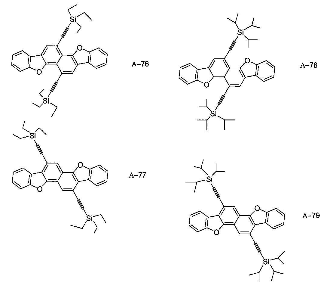
- An alkylsilylethynyl group having 5 to 60 carbon atoms, an arylamino group having 3 to 60 carbon atoms, a diarylamino group having 6 to 120 carbon atoms, or a cyano group, Substituent may have.
- each X 2 represents an oxygen atom or a group represented by N—R 33 .
- R 21 to R 32 are each a hydrogen atom, a halogen atom, an alkyl group having 1 to 30 carbon atoms, a haloalkyl group having 1 to 30 carbon atoms, an alkoxy group having 1 to 30 carbon atoms, or a haloalkoxy group having 1 to 30 carbon atoms.
- R 33 is a halogen atom, an alkyl group having 1 to 30 carbon atoms, a haloalkyl group having 1 to 30 carbon atoms, an alkoxy group having 1 to 30 carbon atoms, a haloalkoxy group having 1 to 30 carbon atoms, or an alkyl group having 1 to 30 carbon atoms.
- both X 2 are groups represented by N—R 33 , the two R 33 may be the same or different.
- An organic thin film transistor material comprising a compound represented by the formula (1) or the formula (2) described in the item 1 or 2. 4). In the organic thin film transistor in which at least three terminals of a gate electrode, a source electrode and a drain electrode, an insulator layer, and an organic semiconductor layer are provided on a substrate, and a source-drain current is controlled by applying a voltage to the gate electrode.
- the organic thin film transistor according to 4 which emits light by using a current flowing between a source and a drain and controls light emission by applying a voltage to a gate electrode. 6).
- the organic thin film transistor according to 5 wherein one of the source electrode and the drain electrode is made of a material having a work function of 4.2 eV or more, and the other is made of a material having a work function of 4.3 eV or less. 7).
- An apparatus comprising the organic thin film transistor according to any one of 8.4 to 7.
- a novel organic thin film transistor material having high carrier mobility can be provided.
- the organic thin film transistor compound of the present invention is represented by the following formula (1).
- each X 1 is an oxygen atom or a group represented by N—R 13 .
- R 1 to R 13 are each a hydrogen atom, a halogen atom, an alkyl group having 1 to 30 carbon atoms, a haloalkyl group having 1 to 30 carbon atoms, an alkoxy group having 1 to 30 carbon atoms, or a haloalkoxy group having 1 to 30 carbon atoms.
- An alkylsilylethynyl group having 5 to 60 carbon atoms, an arylamino group having 3 to 60 carbon atoms, a diarylamino group having 6 to 120 carbon atoms, or a cyano group, Substituent may have.
- R 13 is an alkyl group or an aryl group
- the stability of the compound is maintained, and at the same time, the overlap of ⁇ -conjugated systems between molecules becomes moderate and the carrier mobility may be improved.
- X 1 is a group represented by N—R 13
- two R 13 may be the same or different.
- polycyclic fused-ring compound of this invention is represented by following formula (2). This compound is included in the compound of formula (1).
- each X 2 is an oxygen atom or a group represented by N—R 33 .
- R 21 to R 32 are each a hydrogen atom, a halogen atom, an alkyl group having 1 to 30 carbon atoms, a haloalkyl group having 1 to 30 carbon atoms, an alkoxy group having 1 to 30 carbon atoms, or a haloalkoxy group having 1 to 30 carbon atoms.
- R 33 is a halogen atom, an alkyl group having 1 to 30 carbon atoms, a haloalkyl group having 1 to 30 carbon atoms, an alkoxy group having 1 to 30 carbon atoms, a haloalkoxy group having 1 to 30 carbon atoms, or an alkyl group having 1 to 30 carbon atoms.
- R 33 is an alkyl group or an aryl group, the stability of the compound is maintained, and at the same time, the overlap of ⁇ conjugation between molecules becomes moderate and the carrier mobility may be improved. Preferred as a material.
- both X 2 are groups represented by N—R 33 , the two R 33 may be the same or different.
- the compound of the present invention has a phenacene type structure, it is expected to be superior in storage stability compared to the acene type.
- those having a substituent can be applied to a solution process in which the compound of the present invention is dissolved in a solvent to form an organic semiconductor layer, so that the manufacturing method of the organic TFT is diversified. It is more preferable that it is a linear substituent.
- an alkyl chain such as an alkyl group, a haloalkyl group, an alkoxy group, or an alkylthio group
- solubility is increased by using a branched alkyl group.
- an alkyl chain having an appropriate length for example, an alkyl chain having about 4 to 15 carbon atoms is preferable.
- halogen atom examples include fluorine, chlorine, bromine and iodine atoms.
- alkyl group examples include methyl group, ethyl group, propyl group, isopropyl group, n-butyl group, s-butyl group, isobutyl group, t-butyl group, n-pentyl group, n-hexyl group, and n-heptyl group.
- N-octyl group N-octyl group, n-nonyl group, n-decyl group, n-undecyl group, n-dodecyl group, n-tridecyl group, n-tetradecyl group, n-pentadecyl group, n-hexadecyl group, n-heptadecyl group N-octadecyl group, n-nonadecyl group, n-icosane group, n-henicosane group, n-docosane group, n-tricosane group, n-tetracosane group, n-pentacosane group, n-hexacosane group, n-heptacosane group N-octacosane group, n-nonacosane group, n-triacontan
- haloalkyl group examples include chloromethyl group, 1-chloroethyl group, 2-chloroethyl group, 2-chloroisobutyl group, 1,2-dichloroethyl group, 1,3-dichloroisopropyl group, 2,3-dichloro- t-butyl group, 1,2,3-trichloropropyl group, bromomethyl group, 1-bromoethyl group, 2-bromoethyl group, 2-bromoisobutyl group, 1,2-dibromoethyl group, 1,3-dibromoisopropyl group, 2,3-dibromo-t-butyl group, 1,2,3-tribromopropyl group, iodomethyl group, 1-iodoethyl group, 2-iodoethyl group, 2-iodoisobutyl group, 1,2-diiodoethyl group, 1, 3-diio
- the alkoxy group is a group represented by —OY 1
- examples of Y 1 include the same examples as described for the alkyl group
- the haloalkoxy group is represented by —OY 2.
- Examples of Y 2 include the same examples as those described for the haloalkyl group.
- the alkylthio group is a group represented by —SY 1
- examples of Y 1 include the same examples as described for the alkyl group
- the haloalkylthio group is represented by —SY 2.
- Examples of Y 2 include the same examples as those described for the haloalkyl group.
- the alkylamino group is a group represented by —NHY 1 ; the dialkylamino group is a group represented by —NY 1 Y 3 ; and Y 1 and Y 3 are the same as those described for the alkyl group, respectively. Similar examples are given.
- the alkyl group of the dialkylamino group may be bonded to each other to form a ring structure containing a nitrogen atom, and examples of the ring structure include pyrrolidine, piperidine and the like.
- the alkylsulfonyl group is a group represented by —SO 2 Y 1 , and examples of Y 1 include the same examples as described for the alkyl group, and the haloalkylsulfonyl group includes —SO 2 Y 2 is a group represented by Y 2 , and examples of Y 2 include the same examples as those described for the haloalkyl group.
- the aryl group is an aromatic hydrocarbon ring and an aromatic heterocycle, and specific examples of the aromatic hydrocarbon ring include benzene, naphthalene, anthracene, chrysene, phenanthrene, tetracene, fluorene, pyrene, fluoranthene, perylene and the like. Is mentioned.
- aromatic heterocycle examples include pyridine, pyrazine, indole, acridine, pyrrole, imidazole, pyrazole, quinoline, naphthyridine, quinoxaline, phenazine, phenothiazine, phenoxazine, diazaanthracene, pyridoquinoline, pyrimidoquinazoline, pyra Dinoquinoxaline, phenanthroline, carbazole, thiophene, benzothiophene, dibenzothiophene, benzodithiophene, [1] benzothieno [3,2-b] benzothiophene, thienothiophene, dithienothiophene, furan, benzofuran, dibenzofuran, benzodifuran, thiazole, Benzothiazole, dithiaindacene, dithiaindenoindene, dibenzoselenoph
- the alkylsilyl group is a group represented by —SiY 1 Y 3 Y 4 , and examples of Y 1 , Y 3 and Y 4 are the same as those described for the alkyl group. For example, a trimethylsilyl group etc. are mentioned.
- the alkylsilylethynyl group is a group in which the group represented by the alkylsilyl group is interposed by an ethynylene group, and examples thereof include a trimethylsilylethynyl group, a triethylsilylethynyl group, and a triisopropylsilylethynyl group.
- the arylamino group is a group represented by —NHY 5
- the diarylamino group is a group represented by —NY 5 Y 6
- Y 5 and Y 6 are those described for the aryl group, respectively. The same example is given.
- Examples of the substituent that may be further substituted for each group represented by R 1 to R 13 in the formula (1) and R 21 to R 33 in the formula (2) include the aromatic hydrocarbon group and the aromatic heterocyclic ring described above.
- Group, alkyl group, alkoxy group, haloalkyl group, alkylthio group, alkylsulfonyl group, aryloxy group, arylthio group, alkoxycarbonyl group, amino group, halogen atom, cyano group, nitro group, hydroxyl group, carboxyl group, etc. Can be mentioned.
- the organic compound having a specific structure used in the organic thin film transistor of the present invention is basically bipolar with p-type (hole conduction) and n-type (electron conduction), and is combined with the source and drain electrodes described later. Therefore, it can be driven as a p-type element or an n-type element.
- the lowest unoccupied orbital (LUMO) level is lowered to function as an n-type semiconductor.
- Preferred as the electron-accepting group are a hydrogen atom, a halogen atom, a cyano group, a haloalkyl group having 1 to 30 carbon atoms, a haloalkoxy group having 1 to 30 carbon atoms, and a haloalkylsulfonyl group having 1 to 30 carbon atoms.
- the highest occupied orbital (HOMO) level can be increased to function as a p-type semiconductor.
- Preferred examples of the electron donating group include a hydrogen atom, an alkyl group having 1 to 30 carbon atoms, an alkoxy group having 1 to 30 carbon atoms, an alkylamino group having 1 to 30 carbon atoms, and a dialkylamino group having 2 to 60 carbon atoms.
- the amino groups may be bonded to each other to form a ring structure containing a nitrogen atom).
- N— such as (B-1) means “N—CH 3 ”.
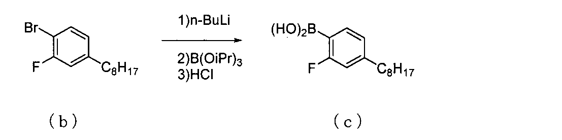
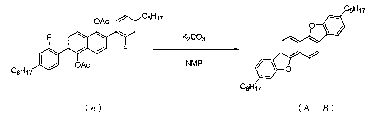
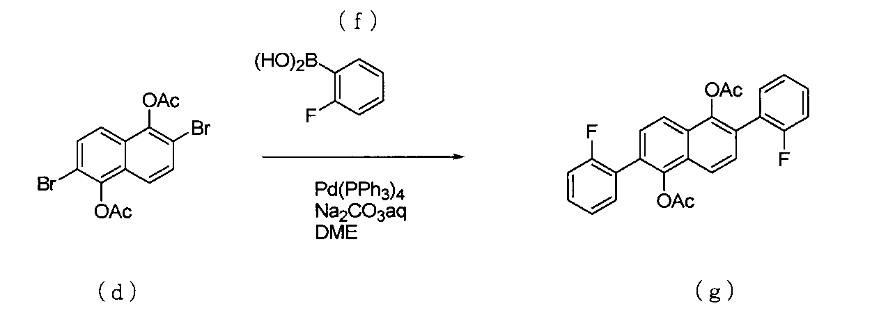
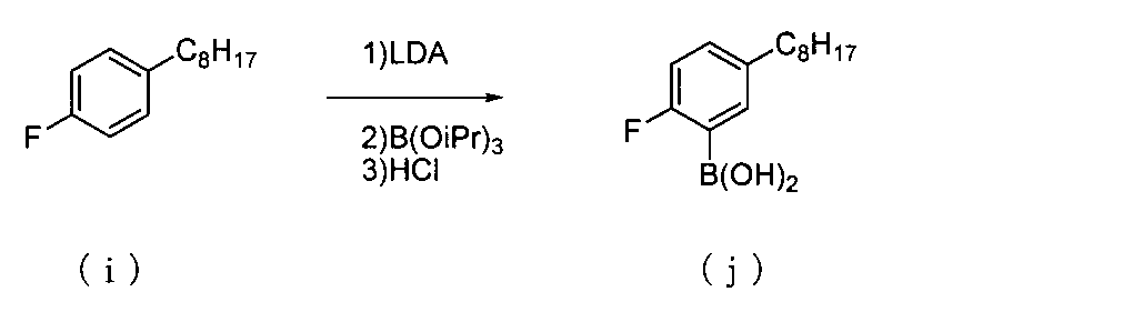
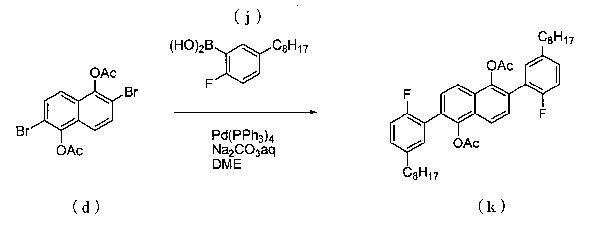
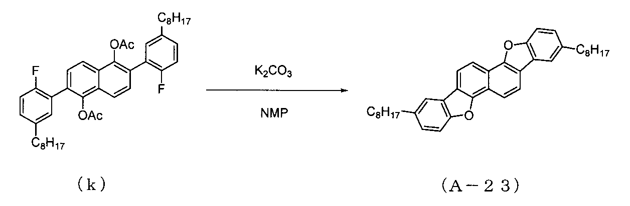
- the polycyclic fused ring compound of the present invention used a known method, for example, boronic acid synthesis as shown in the following reaction (A), acetyl protection reaction as shown in (B), and transition metal as shown in (C). It can be synthesized by a Suzuki coupling reaction or a cyclization reaction such as (D).
- an electronic device such as a transistor
- a device with high field-effect mobility and a high on / off ratio can be obtained by using a material with high purity. Therefore, it is desirable to add purification by techniques such as column chromatography, recrystallization, distillation, sublimation, etc. as necessary. Preferably, it is possible to improve the purity by repeatedly using these purification methods or combining a plurality of methods. Furthermore, it is desirable to repeat sublimation purification at least twice as a final step of purification. By using these methods, it is preferable to use a material having a purity of 90% or more measured by HPLC, more preferably 95% or more, and particularly preferably 99% or more. In addition, the on / off ratio can be increased and the performance inherent to the material can be extracted.
- the element configuration of the organic thin film transistor of the present invention is such that at least three terminals of a gate electrode, a source electrode and a drain electrode, an insulator layer and an organic semiconductor layer are provided on a substrate, and a source-drain current is applied to the gate electrode. It is a thin film transistor controlled by this. And an organic-semiconductor layer contains the compound for organic thin-film transistors of this invention mentioned above, It is characterized by the above-mentioned.
- the structure of the transistor is not particularly limited, and components other than the components of the organic semiconductor layer may have a known element configuration. A specific example of the element configuration of the organic thin film transistor will be described with reference to the drawings.
- the organic thin film transistor 1 of FIG. 1 has a source electrode 11 and a drain electrode 12 formed on a substrate 10 so as to face each other with a predetermined interval. And the organic-semiconductor layer 13 is formed so that the source electrode 11, the drain electrode 12, and the gap
- a gate electrode 15 is formed on the insulator layer 14 and on the gap between the source electrode 11 and the drain electrode 12.
- the organic thin film transistor 2 in FIG. 2 has a gate electrode 15 and an insulator layer 14 in this order on a substrate 10, and a pair of source electrode 11 and drain formed on the insulator layer 14 with a predetermined interval therebetween.
- An electrode 12 is provided, and an organic semiconductor layer 13 is formed thereon.
- the organic semiconductor layer 13 forms a channel region, and is turned on / off by controlling a current flowing between the source electrode 11 and the drain electrode 12 with a voltage applied to the gate electrode 15.
- the organic thin film transistor 3 in FIG. 3 has a gate electrode 15, an insulator layer 14, and an organic semiconductor layer 13 in this order on a substrate 10.
- a source electrode 11 and a drain electrode 12 are provided.
- the insulating layer 14 and the gate electrode 15 are provided in this order.
- the organic thin film transistor of the present invention has a field effect transistor (FET: Field Effect Transistor) structure. As described above, there are several configurations depending on the position of the electrodes, the layer stacking order, and the like.
- the organic thin film transistor is formed with an organic semiconductor layer (organic compound layer), a source electrode and a drain electrode formed to face each other with a predetermined distance, and a predetermined distance from the source electrode and the drain electrode. And a current flowing between the source and drain electrodes is controlled by applying a voltage to the gate electrode.
- the distance between the source electrode and the drain electrode is determined by the use of the organic thin film transistor of the present invention, and is usually 0.1 ⁇ m to 1 mm, preferably 1 ⁇ m to 100 ⁇ m, and more preferably 5 ⁇ m to 100 ⁇ m.
- the organic thin film transistor of the present invention has also been proposed as the organic thin film transistor in the above device configuration, and the current flowing between the source electrode and the drain electrode is controlled by the voltage applied to the gate electrode.
- the device configuration is not limited to the above as long as an effect such as on / off operation and amplification is exhibited.
- the top-and-bottom contact type organic thin film transistor 5 (Fig. 5) proposed by Yoshida et al. Of the National Institute of Advanced Industrial Science and Technology in the 49th Applied Physics Related Conference Lecture Collection 27a-M-3 (March 2002)
- a vertical organic thin film transistor 6 proposed by Kudo et al. Of Chiba University in the IEEJ Transactions 118-A (1998), page 1440.
- the constituent members of the organic thin film transistor will be described.
- the organic-semiconductor layer in the organic thin-film transistor of this invention contains the compound for organic thin-film transistors of this invention mentioned above.
- the thickness of the organic semiconductor layer is not particularly limited, but is usually 0.5 nm to 1 ⁇ m, preferably 2 nm to 250 nm.
- a method for forming the organic semiconductor layer is not particularly limited, and a known method can be applied.
- the organic semiconductor layer material is formed as described above.
- the solvent used in the case of forming the organic semiconductor by dissolving the organic semiconductor material in the solvent is not particularly limited. Examples thereof include alcohol solvents, ketone solvents, hydrocarbon solvents, halogenated hydrocarbon solvents, nitrile solvents, and aprotic polar solvents.
- the annealing temperature is preferably 50 to 200 ° C., more preferably 70 to 200 ° C., and the time is preferably 10 minutes to 12 hours, more preferably 1 to 10 hours.
- the organic semiconductor layer one kind of the compound represented by the formula (1) may be used, or a plurality of mixed thin films or stacked layers using a known semiconductor such as pentacene or thiophene oligomer may be used. May be used.
- the substrate in the organic thin film transistor of the present invention plays a role of supporting the structure of the organic thin film transistor.
- a material in addition to glass, inorganic compounds such as metal oxides and nitrides, plastic films (PET, PES, PC) It is also possible to use metal substrates or composites or laminates thereof.
- PET, PES, PC plastic films
- metal substrates or composites or laminates thereof when the structure of the organic thin film transistor can be sufficiently supported by the components other than the substrate, it is possible not to use the substrate.
- a silicon (Si) wafer is often used as a material for the substrate.
- Si itself can be used as a gate electrode / substrate.
- the surface of Si can be oxidized to form SiO 2 and used as an insulating layer.
- a metal layer such as Au may be formed on the Si substrate serving as the substrate and gate electrode as an electrode for connecting the lead wire.
- the material for the gate electrode, the source electrode and the drain electrode is not particularly limited as long as it is a conductive material.
- Examples of the method for forming the electrode include means such as vapor deposition, electron beam vapor deposition, sputtering, atmospheric pressure plasma method, ion plating, chemical vapor deposition, electrodeposition, electroless plating, spin coating, printing, and ink jet. It is done.
- a conductive thin film formed using the above method is formed using a known photolithographic method or a lift-off method, on a metal foil such as aluminum or copper.
- the thickness of the electrode formed in this way is not particularly limited as long as current is conducted, but is preferably in the range of 0.2 nm to 10 ⁇ m, more preferably 4 nm to 300 nm. If it is in this preferable range, the resistance is increased due to the thin film thickness, and a voltage drop does not occur. In addition, since the film is not too thick, it does not take time to form the film, and when another layer such as a protective layer or an organic semiconductor layer is laminated, the laminated film can be smooth without causing a step.
- another source electrode, drain electrode, gate electrode and a method for forming the source electrode are formed using a fluid electrode material such as a solution, paste, ink, or dispersion containing the above conductive material.
- a fluid electrode material such as a solution, paste, ink, or dispersion containing the above conductive material.
- a fluid electrode material containing a conductive polymer or metal fine particles containing platinum, gold, silver, or copper is preferable.
- the solvent or dispersion medium is preferably a solvent or dispersion medium containing 60% by mass or more, preferably 90% by mass or more of water, in order to suppress damage to the organic semiconductor.
- the dispersion containing the metal fine particles for example, a known conductive paste or the like may be used, but a dispersion containing metal fine particles having a particle size of usually 0.5 nm to 50 nm, 1 nm to 10 nm is preferable.
- the material of the metal fine particles include platinum, gold, silver, nickel, chromium, copper, iron, tin, antimony, lead, tantalum, indium, palladium, tellurium, rhenium, iridium, aluminum, ruthenium, germanium, molybdenum, Tungsten, zinc, or the like can be used.
- an electrode using a dispersion in which these metal fine particles are dispersed in water or a dispersion medium which is an arbitrary organic solvent using a dispersion stabilizer mainly composed of an organic material.
- a method for producing such a dispersion of metal fine particles metal ions can be reduced in the liquid phase, such as a physical generation method such as gas evaporation method, sputtering method, metal vapor synthesis method, colloid method, coprecipitation method, etc.
- a chemical production method for producing metal fine particles preferably disclosed in JP-A-11-76800, JP-A-11-80647, JP-A-11-319538, JP-A-2000-239853, and the like.
- metal fine particle dispersions may be directly patterned by an ink jet method, or may be formed from a coating film by lithograph or laser ablation. Moreover, the patterning method by printing methods, such as a letterpress, an intaglio, a lithographic plate, and screen printing, can also be used. After the electrode is formed and the solvent is dried, the metal fine particles are heat-fused by heating in a shape within a range of 100 ° C. to 300 ° C., preferably 150 ° C. to 200 ° C., if necessary. An electrode pattern having the following shape can be formed.
- a known conductive polymer whose conductivity has been improved by doping is also preferable to use as another gate electrode, source electrode, and drain electrode material.
- conductive polyaniline, conductive polypyrrole, conductive polythiophene, A complex of polyethylene dioxythiophene (PEDOT) and polystyrene sulfonic acid is also preferably used. These materials can reduce the contact resistance between the organic semiconductor layer of the source electrode and the drain electrode.
- These forming methods may also be patterned by an ink jet method, or may be formed from a coating film by lithography, laser ablation, or the like.
- the patterning method by printing methods such as a letterpress, an intaglio, a lithographic plate, and screen printing, can also be used.
- the material for forming the source electrode and the drain electrode is preferably a material having a small electric resistance at the contact surface with the organic semiconductor layer among the examples described above.
- the electrical resistance at this time corresponds to the field effect mobility when the current control device is manufactured, and the resistance needs to be as small as possible in order to obtain a large mobility.
- This is generally determined by the magnitude relationship between the work function of the electrode material and the energy level of the organic semiconductor layer.
- the work function (W) of the electrode material is a
- the ionization potential of the organic semiconductor layer is (Ip) b
- the electron affinity (Af) of the organic semiconductor layer is c
- the following relational expression is preferably satisfied.
- a, b, and c are all positive values based on the vacuum level.
- ba ⁇ 1.5 eV (formula (I)) is preferable, and ba ⁇ 1.0 eV is more preferable. If the above relationship can be maintained in relation to the organic semiconductor layer, a high-performance device can be obtained.
- the electrode material has a work function as large as possible, and the work function is 4.0 eV or more.
- the work function is preferably 4.2 eV or more.
- the value of the work function of a metal is, for example, an effective metal having a work function of 4.0 eV or higher as described in Chemistry Handbook Fundamentals II-493 (revised 3 edition, published by The Chemical Society of Japan, Maruzen 1983)
- the high work function metal is mainly Ag (4.26, 4.52, 4.64, 4.74 eV), Al (4.06, 4.24, 4.41 eV), Au (5.1, 5.37, 5.47 eV), Be (4.98 eV), Bi (4.34 eV), Cd (4.08 eV), Co (5.0 eV), Cu (4.65 eV), Fe (4.5, 4.67, 4.81 eV), Ga (4.3 eV), Hg (4.4 eV), Ir (5.42, 5.76 eV), Mn (4.1 eV), Mo (4 .53, 4.55, 4.95 eV), Nb (4.02, 4.3) , 4.87 eV), Ni (5.04, 5.22, 5.35 eV), Os (5.93
- the work function of the electrode material is preferably as small as possible, and the work function is preferably 4.3 eV or less. More preferably, the work function is 3.7 eV or less.
- the low work function metal it has a work function of 4.3 eV or less as described in, for example, Chemical Handbook, Basics, pages II-493 (revised 3rd edition, published by The Chemical Society of Japan, Maruzen Co., Ltd.
- the electrode material contains one or more of these low work function substances, there is no particular limitation as long as the work function satisfies the above formula (II).
- the low work function metal easily deteriorates when exposed to moisture and oxygen in the atmosphere, it is desirable to coat with a stable metal in the air such as Ag or Au as necessary.
- the film thickness necessary for the coating is 10 nm or more, and as the film thickness increases, the film can be protected from oxygen and water. However, for practical reasons, the thickness is preferably 1 ⁇ m or less for the purpose of increasing productivity.
- a buffer layer may be provided between the organic semiconductor layer and the source and drain electrodes for the purpose of improving the injection efficiency.
- the buffer layer for n-type organic thin film transistors, LiF, Li 2 O, CsF, Na 2 CO 3 , KCl, MgF 2 , CaCO 3 and other alkali metal and alkaline earth metal ion bonds used for the cathode of organic EL A compound having Moreover, you may insert the compound used as an electron injection layer and an electron carrying layer by organic EL, such as Alq.
- cyano compounds such as FeCl 3 , TCNQ, F 4 -TCNQ, HAT, CFx, GeO 2 , SiO 2 , MoO 3 , V 2 O 5 , VO 2 , V 2 O 3 , MnO, Metal oxides other than alkali metals and alkaline earth metals such as Mn 3 O 4 , ZrO 2 , WO 3 , TiO 2 , In 2 O 3 , ZnO, NiO, HfO 2 , Ta 2 O 5 , ReO 3 , PbO 2 Inorganic compounds such as ZnS and ZnSe are desirable. In many cases, these oxides cause oxygen vacancies, which are suitable for hole injection. Further, amine compounds such as TPD and NPD, and compounds used as a hole injection layer and a hole transport layer in an organic EL device such as CuPc may be used. Moreover, what consists of two or more types of said compounds is desirable.
- the buffer layer has the effect of lowering the threshold voltage by lowering the carrier injection barrier and driving the transistor at a low voltage. This is because there is a carrier trap at the interface between the organic semiconductor and the insulator layer.
- the first injected carrier is used to fill the trap, but by inserting a buffer layer, the trap is filled at a low voltage and the mobility is improved.
- the buffer layer only needs to be thin between the electrode and the organic semiconductor layer, and the thickness is 0.1 nm to 30 nm, preferably 0.3 nm to 20 nm.
- the material of the insulator layer in the organic thin film transistor of the present invention is not particularly limited as long as it has electrical insulation and can be formed as a thin film.
- Metal oxide including silicon oxide
- metal nitride (Including silicon nitride)
- polymers low molecular organic molecules, and the like, materials having an electrical resistivity at room temperature of 10 ⁇ cm or more can be used, and an inorganic oxide film having a high relative dielectric constant is particularly preferable.
- Inorganic oxides include silicon oxide, aluminum oxide, tantalum oxide, titanium oxide, tin oxide, vanadium oxide, barium strontium titanate, barium zirconate titanate, lead zirconate titanate, lead lanthanum titanate, strontium titanate, Barium titanate, lanthanum oxide, fluorine oxide, magnesium oxide, bismuth oxide, bismuth titanate, niobium oxide, strontium bismuth titanate, strontium bismuth tantalate, tantalum pentoxide, bismuth tantalate niobate, trioxide Examples thereof include yttrium and combinations thereof, and silicon oxide, aluminum oxide, tantalum oxide, and titanium oxide are preferable.
- inorganic nitrides such as silicon nitride (Si 3 N 4 , SixNy (x, y> 0)) and aluminum nitride can be suitably used.
- the insulator layer may be formed of a precursor containing an alkoxide metal, and the insulator layer is formed by coating a solution of the precursor on a substrate, for example, and subjecting the solution to a chemical solution treatment including heat treatment. It is formed.
- the metal in the alkoxide metal is selected from, for example, a transition metal, a lanthanoid, or a main group element.
- alkoxide in the alkoxide metal examples include, for example, alcohols including methanol, ethanol, propanol, isopropanol, butanol, isobutanol, methoxyethanol, ethoxyethanol, propoxyethanol, butoxyethanol, pentoxyethanol, heptoxyethanol, Examples thereof include those derived from alkoxy alcohols including methoxypropanol, ethoxypropanol, propoxypropanol, butoxypropanol, pentoxypropanol, heptoxypropanol, and the like.
- the insulator layer when the insulator layer is made of the above-described material, polarization easily occurs in the insulator layer, and the threshold voltage for transistor operation can be reduced. Further, among the above materials, in particular, when an insulator layer is formed of silicon nitride such as Si 3 N 4 , SixNy, or SiONx (x, y> 0), a depletion layer is more easily generated, and the threshold of transistor operation is increased. The voltage can be further reduced.
- polyimide, polyamide, polyester, polyacrylate, photo radical polymerization system, photo cation polymerization system photo-curable resin, copolymer containing acrylonitrile component, polyvinyl phenol, polyvinyl alcohol, A novolac resin, cyanoethyl pullulan, or the like can also be used.
- wax polyethylene, polychloropyrene, polyethylene terephthalate, polyoxymethylene, polyvinyl chloride, polyvinylidene fluoride, polysulfone, polyimide cyanoethyl pullulan, poly (vinylphenol) (PVP), poly (methyl methacrylate) (PMMA), polycarbonate (PC ), Polystyrene (PS), polyolefin, polyacrylamide, poly (acrylic acid), novolac resin, resole resin, polyimide, polyxylylene, epoxy resin, and also high molecular materials with high dielectric constant such as pullulan can be used. It is.
- a material having water repellency is particularly preferable.
- the interaction between the insulator layer and the organic semiconductor layer can be suppressed, and the crystallinity of the organic semiconductor layer can be improved by utilizing the cohesiveness inherent in the organic semiconductor, thereby improving the device performance.
- Examples of this include Yasuda et al. Jpn. J. et al. Appl. Phys. Vol. 42 (2003) p. 6614-6618 and Janos Veres et al. Chem. Mater. , Vol. 16 (2004) p. 4543-4555 can be mentioned.
- the organic semiconductor layer can be formed with less damage. Therefore, it is an effective method.
- the insulator layer may be a mixed layer using a plurality of inorganic or organic compound materials as described above, or may be a laminated structure of these. In this case, the performance of the device can be controlled by mixing or laminating a material having a high dielectric constant and a material having water repellency, if necessary.
- the insulator layer may include an anodic oxide film or the anodic oxide film as a configuration.
- the anodized film is preferably sealed.
- the anodized film is formed by anodizing a metal that can be anodized by a known method. Examples of the metal that can be anodized include aluminum and tantalum, and the anodizing method is not particularly limited, and a known method can be used.
- An oxide film is formed by anodizing. Any electrolyte solution that can form a porous oxide film can be used as the anodizing treatment. Generally, sulfuric acid, phosphoric acid, oxalic acid, chromic acid, boric acid, sulfamic acid, benzenesulfone, and the like can be used. An acid or the like or a mixed acid obtained by combining two or more of these or a salt thereof is used.
- the treatment conditions for anodization vary depending on the electrolyte used and cannot be specified in general. In general, however, the concentration of the electrolyte is 1 to 80% by mass, the temperature of the electrolyte is 5 to 70 ° C., and the current density.
- a preferred anodizing treatment is a method in which an aqueous solution of sulfuric acid, phosphoric acid or boric acid is used as the electrolytic solution and the treatment is performed with a direct current, but an alternating current can also be used.
- the concentration of these acids is preferably 5 to 45% by mass, and the electrolytic treatment is preferably performed for 20 to 250 seconds at an electrolyte temperature of 20 to 50 ° C. and a current density of 0.5 to 20 A / cm 2 .
- the thickness of the insulator layer As the thickness of the insulator layer, if the layer thickness is thin, the effective voltage applied to the organic semiconductor increases, so the drive voltage and threshold voltage of the device itself can be lowered, but conversely between the source and gate. Therefore, it is necessary to select an appropriate film thickness, which is normally 10 nm to 5 ⁇ m, preferably 50 nm to 2 ⁇ m, and more preferably 100 nm to 1 ⁇ m.
- any orientation treatment may be performed between the insulator layer and the organic semiconductor layer.
- a preferable example thereof is a method for improving the crystallinity of the organic semiconductor layer by reducing the interaction between the insulator layer and the organic semiconductor layer by performing a water repellent treatment or the like on the surface of the insulator layer.
- Silane coupling agents such as hexamethyldisilazane, octadecyltrichlorosilane, trichloromethylsilazane, and self-organized alignment film materials such as alkane phosphoric acid, alkane sulfonic acid, and alkane carboxylic acid are insulated in a liquid phase or gas phase state.
- An example is a method in which the film is brought into contact with the surface of the film to form a self-assembled film, followed by appropriate drying treatment.
- a method in which a film made of polyimide or the like is provided on the surface of the insulating film and the surface is rubbed so as to be used for liquid crystal alignment is also preferable.
- the insulator layer can be formed by vacuum deposition, molecular beam epitaxy, ion cluster beam, low energy ion beam, ion plating, CVD, sputtering, JP-A-11-61406, 11-133205, JP-A 2000-121804, 2000-147209, 2000-185362, etc., dry process such as atmospheric pressure plasma method, spray coating method, spin coating method, blade coating Examples thereof include wet processes such as a method by coating such as a method, a dip coating method, a cast method, a roll coating method, a bar coating method, and a die coating method, and a patterning method such as printing and ink jetting.
- the wet process is a method of applying and drying a liquid in which fine particles of inorganic oxide are dispersed in an arbitrary organic solvent or water using a dispersion aid such as a surfactant as required, or an oxide precursor, for example,
- a so-called sol-gel method in which a solution of an alkoxide body is applied and dried is used.
- the method for forming the organic thin film transistor of the present invention is not particularly limited, and may be a known method. According to a desired element configuration, the substrate is charged, the gate electrode is formed, the insulator layer is formed, the organic semiconductor layer is formed, and the source electrode is formed. It is preferable to form a series of device manufacturing steps up to the formation of the drain electrode without being exposed to the atmosphere at all, because the device performance can be prevented from being impaired by moisture, oxygen, etc. in the atmosphere due to contact with the atmosphere. If it is unavoidable that the atmosphere must be exposed to the atmosphere once, the steps after the organic semiconductor layer formation are not exposed to the atmosphere at all, and the surface on which the organic semiconductor layer is laminated (for example, FIG. In the case of the organic thin film transistor 2 of FIG.
- the surface of the insulating layer partially laminated with a source electrode and a drain electrode) is cleaned and activated by ultraviolet irradiation, ultraviolet / ozone irradiation, oxygen plasma, argon plasma, etc. It is preferable to laminate the layers.
- some p-type TFT materials are exposed to the atmosphere once, and the performance is improved by adsorbing oxygen or the like. Therefore, depending on the material, the materials are appropriately exposed to the atmosphere.
- a gas barrier layer may be formed on the whole or a part of the outer peripheral surface of the organic transistor element.
- the gas barrier layer As a material for forming the gas barrier layer, those commonly used in this field can be used, and examples thereof include polyvinyl alcohol, ethylene-vinyl alcohol copolymer, polyvinyl chloride, polyvinylidene chloride, and polychlorotrifluoroethylene. . Furthermore, the inorganic substance which has the insulation illustrated in the said insulator layer can also be used.
- an organic thin film light emitting transistor that emits light using a current flowing between a source electrode and a drain electrode and controls light emission by applying a voltage to the gate electrode. That is, an organic thin film transistor can be used as a light emitting element (organic EL). Since the transistor for controlling light emission and the light emitting element can be integrated, the aperture ratio of the display can be improved and the cost can be reduced by the simplification of the manufacturing process, which provides a great practical advantage. When used as an organic light emitting transistor, it is necessary to inject holes from one of the source electrode and the drain electrode and electrons from the other, and the following conditions are preferably satisfied in order to improve the light emitting performance.
- At least one of the source electrode and the drain electrode is a hole injecting electrode in order to improve the hole injecting property.
- a hole injection electrode is an electrode containing a substance having a work function of 4.2 eV or higher.
- at least one of the source electrode and the drain electrode is preferably an electron injectable electrode.
- An electron injecting electrode is an electrode containing a substance having a work function of 4.3 eV or less. More preferably, it is an organic thin film light emitting transistor provided with an electrode in which one is hole injecting and the other is electron injecting.
- the hole injection layer In order to improve the hole injection property, it is preferable to insert a hole injection layer between at least one of the source electrode and the drain electrode and the organic semiconductor layer.
- the hole injection layer include amine-based materials used as a hole injection material and a hole transport material in an organic EL device.
- an electron injecting layer between at least one of the source electrode and the drain electrode and the organic semiconductor layer.
- the electron injection material used for the organic EL element can be used for the electron injection layer as well as the hole. More preferably, one of the electrodes is provided with a hole injection layer and the other electrode is provided with an electron injection layer. It is a thin film light emitting transistor.
- the device using the organic thin film transistor of the present invention may be a device using the organic thin film transistor of the present invention, and examples thereof include a circuit, a personal computer, a display, and a mobile phone.
- Example 4 (Production of organic thin film transistor by vapor deposition process) An organic thin film transistor was produced by the following procedure. The glass substrate was ultrasonically cleaned with a neutral detergent, pure water, acetone and ethanol for 30 minutes each, and then gold (Au) was formed to a thickness of 40 nm by a sputtering method to produce a gate electrode. Next, this substrate was set in a film forming section of a thermal CVD apparatus. On the other hand, 250 mg of polyparaxylene derivative [polyparaxylene chloride (Parylene)] (trade name; diX-C, manufactured by Daisan Kasei Co., Ltd.), which is a raw material for the insulating layer, was placed in a petri dish.
- Parylene polyparaxylene derivative
- diX-C manufactured by Daisan Kasei Co., Ltd.
- the thermal CVD apparatus was evacuated with a vacuum pump and depressurized to 5 Pa, and then the evaporation part was heated to 180 ° C. and the polymerization part was heated to 680 ° C. and left for 2 hours to form an insulating layer having a thickness of 1 ⁇ m on the gate electrode. .
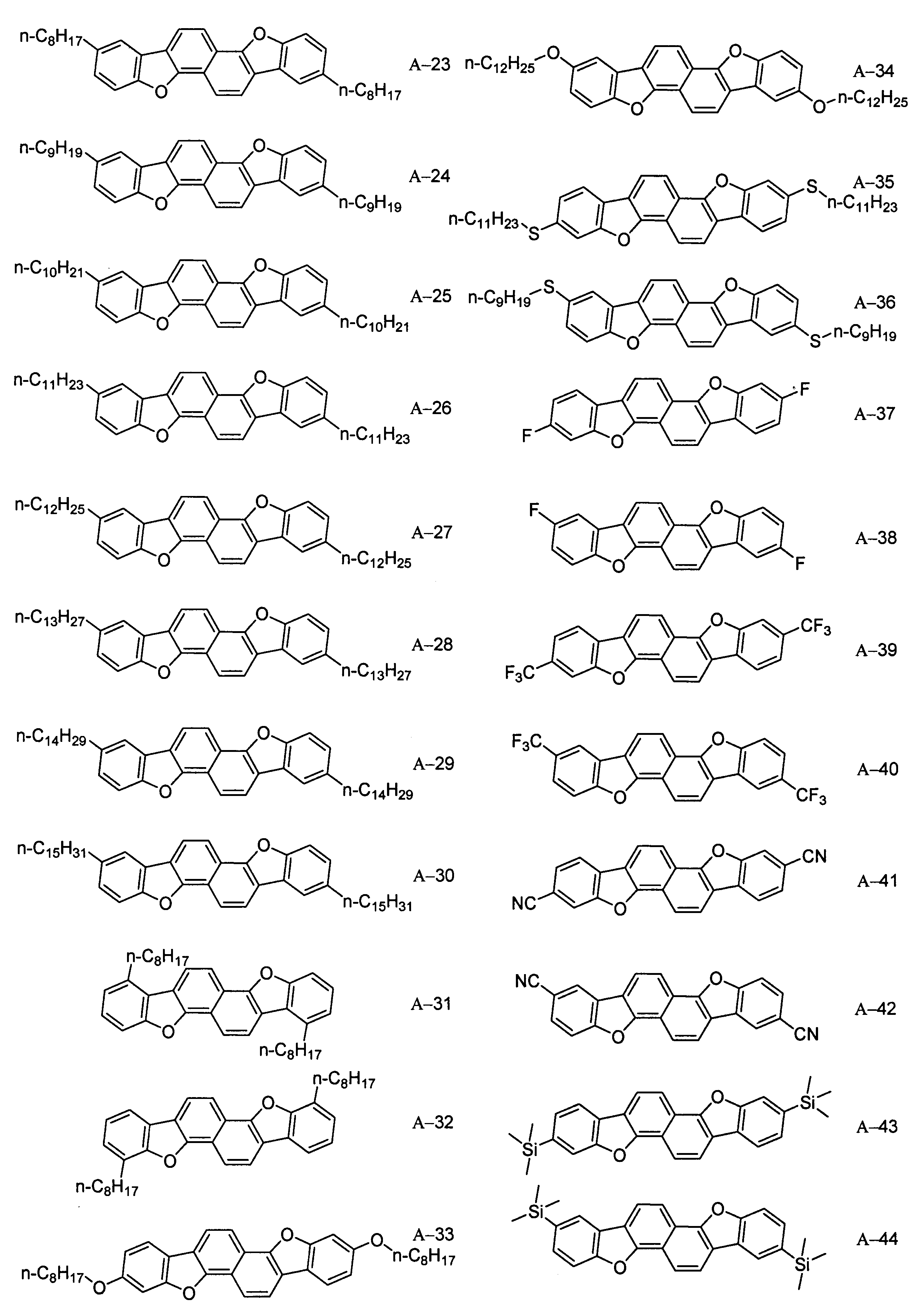
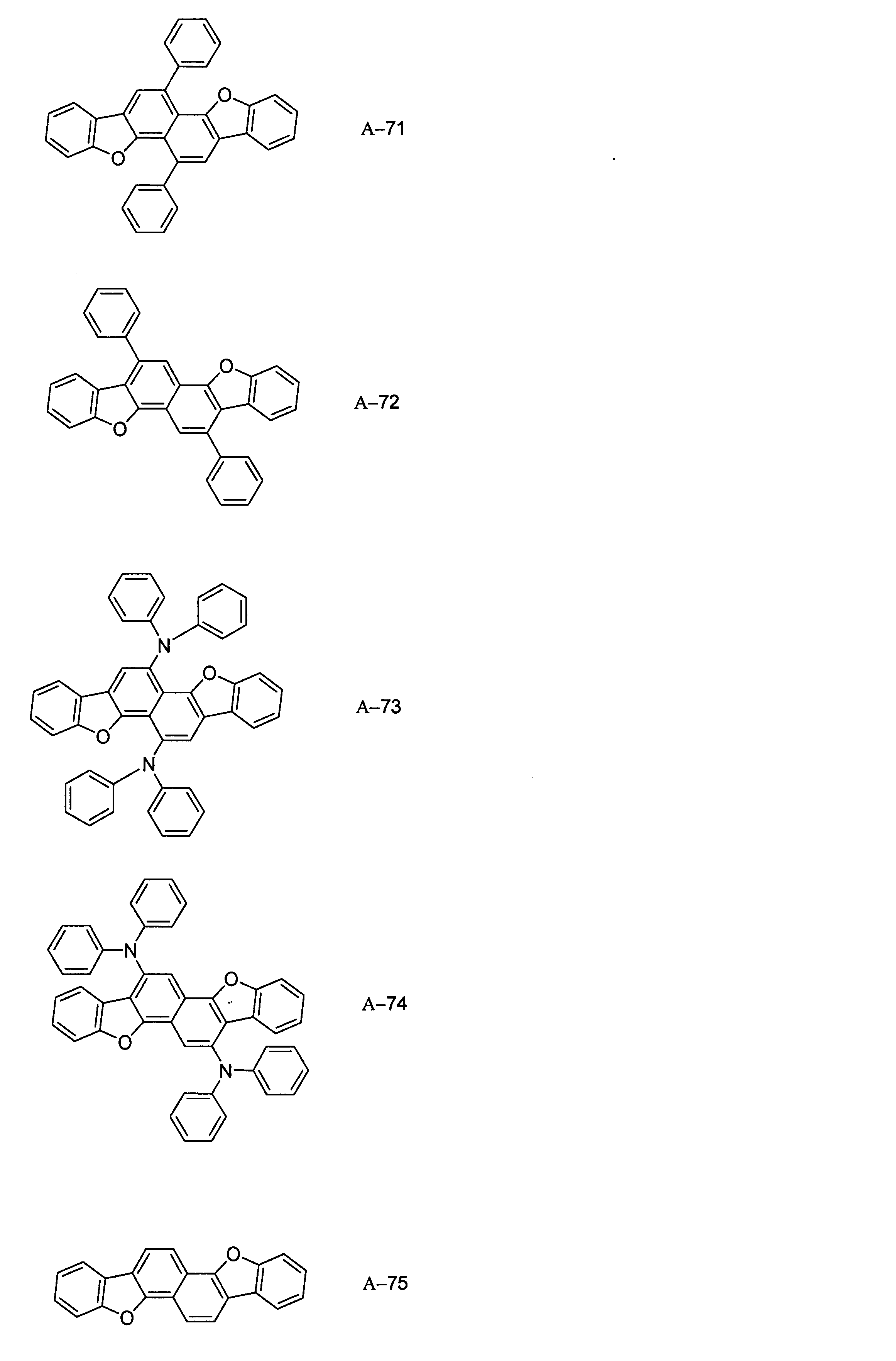
- the substrate was placed in a vacuum vapor deposition apparatus (ULVAC, EX-400), and the compound (A-75) was deposited on the insulator layer with an organic film having a thickness of 50 nm at a deposition rate of 0.05 nm / s.
- a semiconductor layer was formed.
- gold was deposited to a thickness of 50 nm through a metal mask, so that a source electrode and a drain electrode that were not in contact with each other were formed so that a distance (channel length L) was 75 ⁇ m.
- an organic thin film transistor was manufactured by forming a film so that the width (channel width W) of the source electrode and the drain electrode was 5 mm (see FIG. 3).
- the source - a current was passed by applying a voltage between the drain.
- the field effect mobility ⁇ of holes was calculated from the following formula (A) and found to be 1.0 cm 2 / Vs.
- I D (W / 2L) ⁇ C ⁇ ⁇ (V G ⁇ V T ) 2 (A)
- ID is a source-drain current
- W is a channel width
- L is a channel length
- C is a capacitance per unit area of the gate insulator layer
- V T is a gate threshold voltage
- V G is a gate voltage.
- Example 5 (Production of organic thin film transistor by coating process) As in Example 4, the substrate was washed, the gate electrode was formed, and the insulator layer was formed. Next, 0.4% by mass of compound (A-8) was dissolved in toluene, and the film was formed on the substrate on which the insulator layer was formed with a spin coater (Mikasa Co., Ltd .: 1H-D7). It dried at 80 degreeC and formed into a film as an organic-semiconductor layer. Next, gold (Au) was formed in a film thickness of 50 nm through a metal mask with a vacuum deposition apparatus, thereby forming source and drain electrodes that were not in contact with each other, thereby producing an organic thin film transistor.
- a spin coater Moikasa Co., Ltd .: 1H-D7
- the obtained organic thin film transistor was p-type driven at a gate voltage V G of ⁇ 70 V in the same manner as in Example 4.
- Table 1 shows the results of measuring the on / off of the current between the source and drain electrodes and calculating the field effect mobility ⁇ of the holes.
- Example 6 (Production of organic thin film transistor by coating process) An organic thin film transistor was produced in the same manner as in Example 5 except that the compound (A-23) was used instead of the compound (A-8) as the material of the organic semiconductor layer. The obtained organic thin film transistor was p-type driven at a gate voltage V G of ⁇ 70 V in the same manner as in Example 4. Table 1 shows the results of measuring the on / off ratio of the current between the source and drain electrodes and calculating the field effect mobility ⁇ of the holes.
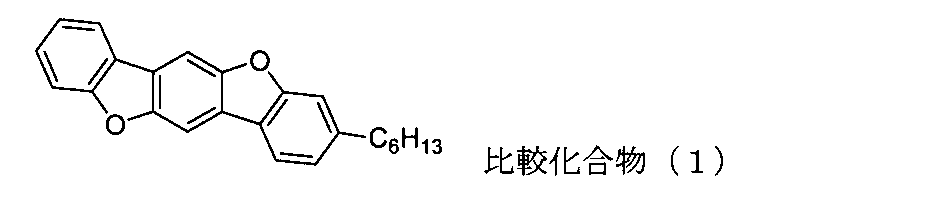
- Comparative Example 1 An organic thin film transistor was produced by the following procedure. First, the surface of a Si substrate (also used as a P-type specific resistance 1 ⁇ cm gate electrode) was oxidized by a thermal oxidation method to produce a 300 nm thermal oxide film on the substrate to form an insulator layer. Further, after the SiO 2 film formed on one side of the substrate was completely removed by dry etching, gold (Au) was further formed thereon by 100 nm sputtering to form an extraction electrode. This substrate was ultrasonically cleaned with a neutral detergent, pure water, acetone and ethanol for 30 minutes each, and further subjected to ozone cleaning.
- a neutral detergent, pure water, acetone and ethanol for 30 minutes each, and further subjected to ozone cleaning.
- the substrate was placed in a vacuum deposition apparatus (ULVAC, EX-400), and the following comparative compound (1) was deposited on the insulator layer at a deposition rate of 0.05 nm / s with a thickness of 50 nm. It formed into a film as an organic-semiconductor layer.
- gold was deposited to a thickness of 50 nm through a metal mask, so that a source electrode and a drain electrode that were not in contact with each other were formed so that a distance (channel length L) was 75 ⁇ m.
- an organic thin film transistor was manufactured by forming a film so that the width (channel width W) of the source electrode and the drain electrode was 5 mm (see FIG. 3).
- the obtained organic thin film transistor was p-type driven at a gate voltage V G of ⁇ 70 V in the same manner as in Example 4.
- Table 1 shows the results of measuring the on / off ratio of the current between the source and drain electrodes and calculating the field effect mobility ⁇ of the holes.
- the organic TFT of the present invention has high carrier mobility, and the compound of this patent is useful as a semiconductor material of the organic TFT.
- the reactor was charged with 25.0 g (143 mmol) of 1-bromo-3-fluorobenzene and purged with nitrogen, and 30 ml of dehydrated THF and 0.82 g (1.0 mmol) of Pd (dppf) Cl 2 .CH 2 Cl 2 were added.
- 110 ml (0.22 mol) of 2M-butylmagnesium chloride was added and stirred at room temperature for 30 minutes, and then heated and stirred at 50 ° C. for 7 hours.
- the reaction mixture was cooled, methanol, pure water, a saturated aqueous NH 4 Cl solution and an aqueous HCl solution were added, and the mixture was extracted with hexane.
- Examples 8 to 14 (Synthesis of compounds (A-5), (A-6), (A-7), (A-9), (A-10), (A-11), (A-12) ) Boronic acid corresponding to each was synthesized in the same manner as in Example 1 or Example 7, and using the boronic acid, the compounds (A-5), (A-6), (A-7), (A-9), (A-10), (A-11), and (A-12) were synthesized. It was confirmed to be the target product by FD-MS measurement. The measurement results of FD-MS are shown below.
- Compound (A-19) was synthesized in the same manner as Example 3 (Synthesis of Compound (A-23)) except that Compound (n) was used instead of Compound (i). It was confirmed to be the target product by FD-MS measurement. The measurement results of FD-MS are shown below.
- Examples 16-22 Synthesis of Compound (A-20), (A-21), (A-22), (A-24), (A-25), (A-26), (A-27) Example 3 or The corresponding boronic acids were synthesized in the same manner as in Example 15, and the compounds (A-20), (A-21), (A-22), (A-24), (A-25), (A-26), and (A-27) were synthesized. It was confirmed to be the target product by FD-MS measurement. The measurement results of FD-MS are shown below.
- Compound (A-48) was synthesized in the same manner as in Example 1 except that compound (o) was used instead of compound (b). It was confirmed to be the target product by FD-MS measurement. The measurement results of FD-MS are shown below.
- the reactor was charged with 50.0 g (0.177 mol) of 1-fluoro-4-iodobenzene, 1.0 g (0.86 mmol) of tetrakistriphenylphosphine palladium (0), 0.33 g (1.73 mmol) of copper (I) iodide. ), 350 ml of diisopropylamine was added, and 21.0 g (0.194 mol) of 1-octyne and 350 ml of dehydrated toluene were added thereto, and the mixture was heated and stirred at 60 ° C. for 6 and a half hours. The reaction mixture was filtered, the solvent of the filtrate was removed under reduced pressure, and purified by column chromatography to obtain 51.6 g of a crude product (p). This crude product was used for the next reaction.
- Compound (A-50) was synthesized in the same manner as in Example 23, except that compound (r) was used instead of 4-octylphenylboronic acid in Example 23. It was confirmed to be the target product by FD-MS measurement. The measurement results of FD-MS are shown below.
- Examples 25 to 38 (Production of organic thin-film transistors by a coating process)
- An organic thin film transistor was fabricated in the same manner as in Example 5 except that each was used.
- the obtained organic thin film transistor was p-type driven at a gate voltage V G of ⁇ 70 V in the same manner as in Example 4.
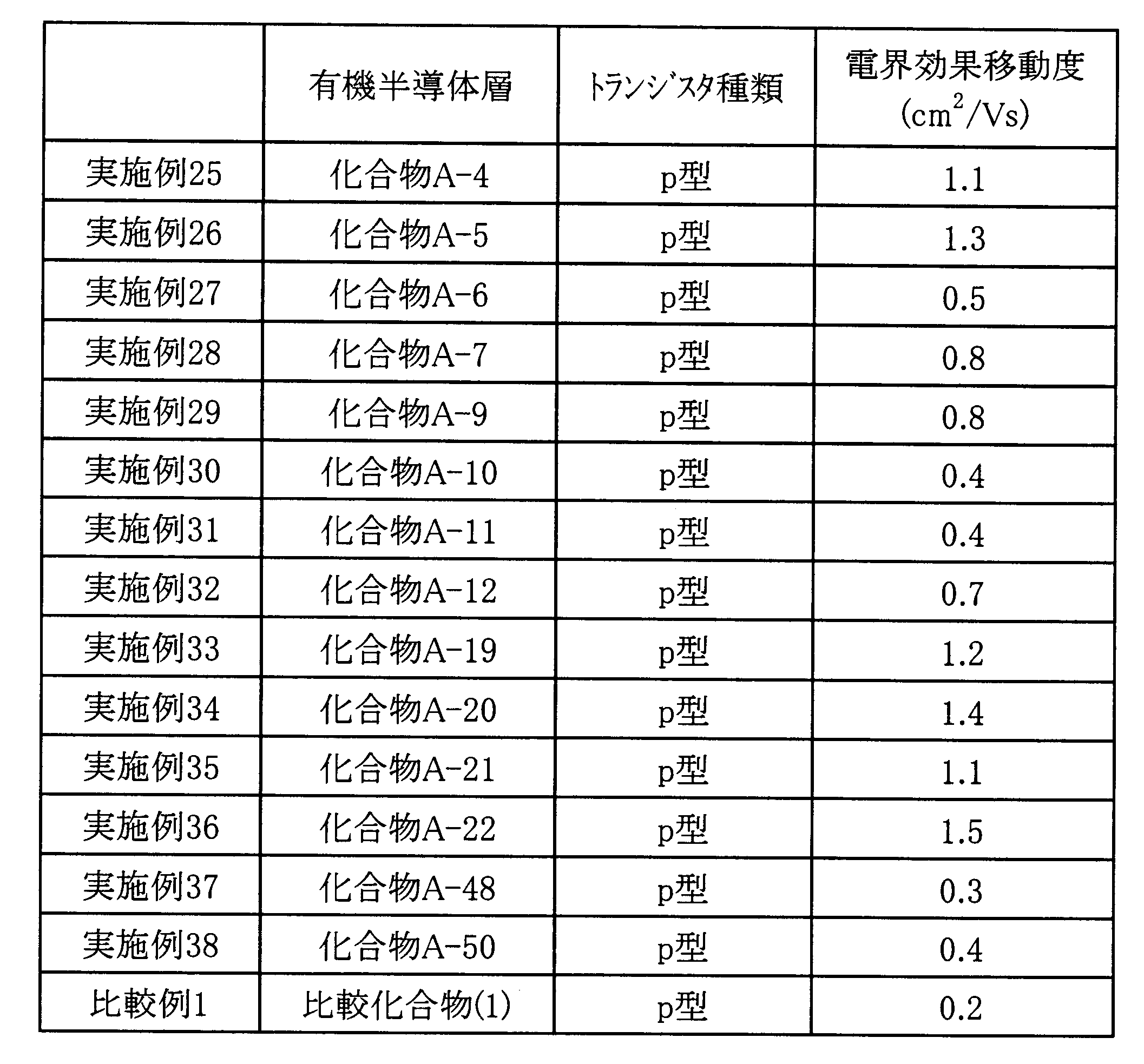
- Table 2 shows the results of measuring the on / off ratio of the current between the source and drain electrodes and calculating the field effect mobility ⁇ of the holes.
- the polycyclic fused ring compound of the present invention can be used as a material for an organic semiconductor layer of an organic thin film transistor. Since the polycyclic fused ring compound of the present invention has high carrier mobility as a material for the organic semiconductor layer, this organic thin film transistor has a high response speed (driving speed) and high performance as a transistor. It can also be used as an organic thin film light emitting transistor capable of emitting light.
Landscapes
- Chemical & Material Sciences (AREA)
- Organic Chemistry (AREA)
- Physics & Mathematics (AREA)
- Spectroscopy & Molecular Physics (AREA)
- Engineering & Computer Science (AREA)
- Materials Engineering (AREA)
- Thin Film Transistor (AREA)
- Heterocyclic Carbon Compounds Containing A Hetero Ring Having Oxygen Or Sulfur (AREA)
Abstract
Description
従来、このTFTは、アモルファスや多結晶のシリコンを用いて作製されていたが、このようなシリコンを用いたTFTの作製に用いられるCVD装置は、非常に高額であり、TFTを用いた表示装置等の大型化は、製造コストの大幅な増加を伴うという問題点があった。また、アモルファスや多結晶のシリコンを成膜するプロセスは非常に高い温度下で行われるので、基板として使用可能な材料の種類が限られてしまうため、軽量な樹脂基板等は使用できないという問題があった。

本発明の目的は、高いキャリア移動度を有する、新規な有機薄膜トランジスタ用材料を提供することである。
1.下記式(1)で表わされる有機薄膜トランジスタ用化合物。
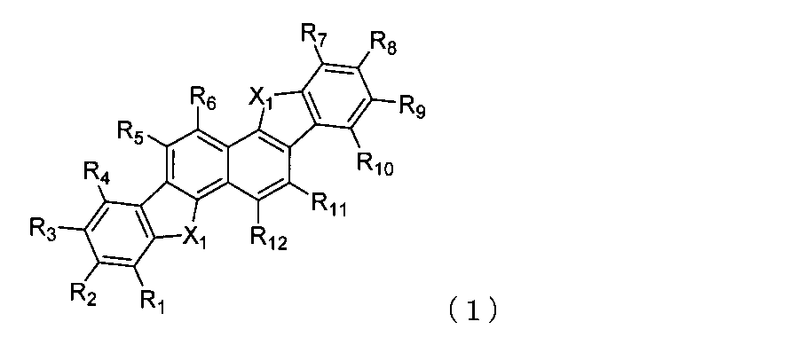
R1~R13は、それぞれ、水素原子、ハロゲン原子、炭素数1~30のアルキル基、炭素数1~30のハロアルキル基、炭素数1~30のアルコキシ基、炭素数1~30のハロアルコキシ基、炭素数1~30のアルキルチオ基、炭素数1~30のハロアルキルチオ基、炭素数1~30のアルキルアミノ基、炭素数2~60のジアルキルアミノ基(アルキル基は互いに結合して窒素原子を含む環構造を形成してもよい)、炭素数1~30のアルキルスルホニル基、炭素数1~30のハロアルキルスルホニル基、炭素数3~60のアリール基、炭素数3~20のアルキルシリル基、炭素数5~60のアルキルシリルエチニル基、炭素数3~60のアリールアミノ基、炭素数6~120のジアリールアミノ基又はシアノ基であり、これら各基は置換基を有していてもよい。
X1がともにN-R13で表わされる基である場合、2つのR13は同一でも異なっていてもよい。]
2.下記式(2)で表される多環縮環化合物。
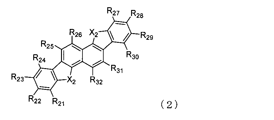
R21~R32は、それぞれ、水素原子、ハロゲン原子、炭素数1~30のアルキル基、炭素数1~30のハロアルキル基、炭素数1~30のアルコキシ基、炭素数1~30のハロアルコキシ基、炭素数1~30のアルキルチオ基、炭素数1~30のハロアルキルチオ基、炭素数1~30のアルキルアミノ基、炭素数2~60のジアルキルアミノ基(アルキル基は互いに結合して窒素原子を含む環構造を形成してもよい)、炭素数1~30のアルキルスルホニル基、炭素数1~30のハロアルキルスルホニル基、炭素数3~60のアリール基、炭素数3~20のアルキルシリル基、炭素数5~60のアルキルシリルエチニル基、炭素数3~60のアリールアミノ基、炭素数6~120のジアリールアミノ基又はシアノ基であり、これら各基は置換基を有していてもよい。
R33は、ハロゲン原子、炭素数1~30のアルキル基、炭素数1~30のハロアルキル基、炭素数1~30のアルコキシ基、炭素数1~30のハロアルコキシ基、炭素数1~30のアルキルチオ基、炭素数1~30のハロアルキルチオ基、炭素数1~30のアルキルアミノ基、炭素数2~60のジアルキルアミノ基(アルキル基は互いに結合して窒素原子を含む環構造を形成してもよい)、炭素数1~30のアルキルスルホニル基、炭素数1~30のハロアルキルスルホニル基、炭素数3~60のアリール基、炭素数3~20のアルキルシリル基、炭素数5~60のアルキルシリルエチニル基、炭素数3~60のアリールアミノ基、炭素数6~120のジアリールアミノ基又はシアノ基であり、これら各基は置換基を有していてもよい。
X2がともにN-R33で表わされる基である場合、2つのR33は同一でも異なっていてもよい。]
3.1又は2に記載の式(1)又は式(2)に示す化合物を含むことを特徴とする有機薄膜トランジスタ用材料。
4.少なくとも基板上にゲート電極、ソース電極及びドレイン電極の3端子、絶縁体層並びに有機半導体層が設けられ、ソース-ドレイン間電流をゲート電極に電圧を印加することによって制御する有機薄膜トランジスタにおいて、前記有機半導体層が、1又は2に記載の式(1)又は式(2)に示す化合物を含む有機薄膜トランジスタ。
5.ソース-ドレイン間を流れる電流を利用して発光し、ゲート電極に電圧を印加することによって発光を制御する4に記載の有機薄膜トランジスタ。
6.ソース電極及びドレイン電極の一方が仕事関数4.2eV以上の物質からなり、他方が仕事関数4.3eV以下の物質からなる5に記載の有機薄膜トランジスタ。
7.ソース及びドレイン電極と有機半導体層の間にバッファ層を有する4~6のいずれかに記載の有機薄膜トランジスタ。
8.4~7のいずれかに記載の有機薄膜トランジスタを備えた装置。
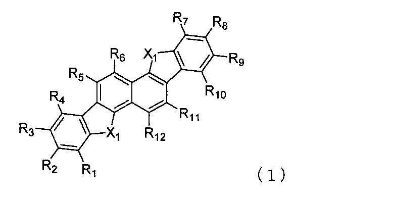
R1~R13は、それぞれ、水素原子、ハロゲン原子、炭素数1~30のアルキル基、炭素数1~30のハロアルキル基、炭素数1~30のアルコキシ基、炭素数1~30のハロアルコキシ基、炭素数1~30のアルキルチオ基、炭素数1~30のハロアルキルチオ基、炭素数1~30のアルキルアミノ基、炭素数2~60のジアルキルアミノ基(アルキル基は互いに結合して窒素原子を含む環構造を形成してもよい)、炭素数1~30のアルキルスルホニル基、炭素数1~30のハロアルキルスルホニル基、炭素数3~60のアリール基、炭素数3~20のアルキルシリル基、炭素数5~60のアルキルシリルエチニル基、炭素数3~60のアリールアミノ基、炭素数6~120のジアリールアミノ基又はシアノ基であり、これら各基は置換基を有していてもよい。
R13が、アルキル基又はアリール基である場合、化合物の安定性が保たれると同時に、分子間におけるπ共役系の重なりが適度となり、キャリア移動度が向上する可能性があるので有機薄膜トランジスタの半導体材料として好ましい。
X1がともにN-R13で表わされる基である場合、2つのR13は同一でも異なっていてもよい。
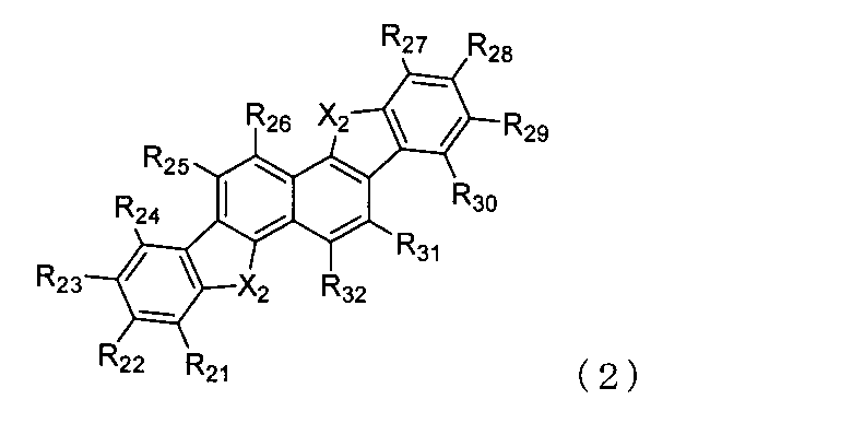
R21~R32は、それぞれ、水素原子、ハロゲン原子、炭素数1~30のアルキル基、炭素数1~30のハロアルキル基、炭素数1~30のアルコキシ基、炭素数1~30のハロアルコキシ基、炭素数1~30のアルキルチオ基、炭素数1~30のハロアルキルチオ基、炭素数1~30のアルキルアミノ基、炭素数2~60のジアルキルアミノ基(アルキル基は互いに結合して窒素原子を含む環構造を形成してもよい)、炭素数1~30のアルキルスルホニル基、炭素数1~30のハロアルキルスルホニル基、炭素数3~60のアリール基、炭素数3~20のアルキルシリル基、炭素数5~60のアルキルシリルエチニル基、炭素数3~60のアリールアミノ基、炭素数6~120のジアリールアミノ基又はシアノ基であり、これら各基は置換基を有していてもよい。
R33が、アルキル基又はアリール基である場合、化合物の安定性が保たれると同時に、分子間におけるπ共役の重なりが適度となり、キャリア移動度が向上する可能性があるので有機薄膜トランジスタの半導体材料として好ましい。
X2がともにN-R33で表わされる基である場合、2つのR33は同一でも異なっていてもよい。
このような観点より、式(1)のR1~R12の位置、そして式(2)のR21~R32の位置が直鎖状の置換基であることが好ましい。
一方、アルキル基が短いほど素子の耐熱性が高くなることが期待でき、アルキル基が長いほどアルキル鎖の相互作用により結晶のパッキングが密となり、移動度が向上する可能性がある。この場合、適度な長さのアルキル鎖、例えば、炭素数4~15程度のアルキル鎖であると好ましい。





本発明の有機薄膜トランジスタの素子構成は、少なくとも基板上にゲート電極、ソース電極及びドレイン電極の3端子、絶縁体層並びに有機半導体層が設けられ、ソース-ドレイン間電流をゲート電極に電圧を印加することによって制御する薄膜トランジスタである。そして、有機半導体層が上述した本発明の有機薄膜トランジスタ用化合物を含むことを特徴とする。
トランジスタの構造は、特に限定されず、有機半導体層の成分以外が公知の素子構成を有するものであってもよい。有機薄膜トランジスタの素子構成の具体例を図を用いて説明する。
図1の有機薄膜トランジスタ1は、基板10上に、相互に所定の間隔をあけて対向するように形成されたソース電極11及びドレイン電極12を有する。そして、ソース電極11、ドレイン電極12及びそれらの間の間隙を覆うように有機半導体層13が形成され、さらに、絶縁体層14が積層されている。絶縁体層14の上部であって、かつソース電極11及びドレイン電極12の間の間隙上にゲート電極15が形成されている。
例えば、産業技術総合研究所の吉田らにより第49回応用物理学関係連合講演会講演予稿集27a-M-3(2002年3月)において提案されたトップアンドボトムコンタクト型有機薄膜トランジスタ5(図5参照)や、千葉大学の工藤らにより電気学会論文誌118-A(1998)1440頁において提案された縦形の有機薄膜トランジスタ6(図6参照)のような素子構成を有するものであってもよい。
以下、有機薄膜トランジスタの構成部材について説明する。
本発明の有機薄膜トランジスタにおける有機半導体層は、上述した本発明の有機薄膜トランジスタ用化合物を含む。有機半導体層の膜厚は、特に制限されることはないが、通常、0.5nm~1μmであり、2nm~250nmであると好ましい。
また、有機半導体層の形成方法は特に限定されることはなく公知の方法を適用でき、例えば、分子線蒸着法(MBE法)、真空蒸着法、化学蒸着、材料を溶媒に溶かした溶液のディッピング法、スピンコーティング法、キャスティング法、バーコート法、ロールコート法、インクジェット法等の印刷、塗布法及びベーキング、エレクトロポリマラインゼーション、分子ビーム蒸着、溶液からのセルフ・アセンブリ、及びこれらの組合せた手段により、前記したような有機半導体層の材料で形成される。
上記の形成方法において、有機半導体材料を溶媒に溶解させて有機半導体を形成する場合において使用する溶媒は特に限定されない。例えば、アルコール系溶媒、ケトン系溶媒、炭化水素系溶媒、ハロゲン化炭化水素系溶媒、ニトリル系溶媒、非プロトン系極性溶媒が挙げられる。
有機半導体層の結晶性を向上させると電界効果移動度が向上するため、成膜方法に関わらず成膜後にアニーリングを実施すると高性能デバイスが得られるため好ましい。アニーリングの温度は50~200℃が好ましく、70~200℃であるとさらに好ましく、時間は10分~12時間が好ましく、1~10時間であるとさらに好ましい。
本発明において、有機半導体層には、式(1)で示される化合物の1種類を用いてもよく、複数を組み合わせたり、ペンタセンやチオフェンオリゴマー等の公知の半導体を用いて複数の混合薄膜又は積層して用いてもよい。
本発明の有機薄膜トランジスタにおける基板は、有機薄膜トランジスタの構造を支持する役目を担うものであり、材料としてはガラスの他、金属酸化物や窒化物等の無機化合物、プラスチックフィルム(PET,PES,PC)や金属基板又はこれら複合体や積層体等も用いることが可能である。また、基板以外の構成要素により有機薄膜トランジスタの構造を十分に支持し得る場合には、基板を使用しないことも可能である。また、基板の材料としてはシリコン(Si)ウエハが用いられることが多い。この場合、Si自体をゲート電極兼基板として用いることができる。また、Siの表面を酸化し、SiO2を形成して絶縁層として活用することも可能である。この場合、基板兼ゲート電極のSi基板にリード線接続用の電極として、Au等の金属層を成膜することもある。
本発明の有機薄膜トランジスタにおける、ゲート電極、ソース電極及びドレイン電極の材料としては、導電性材料であれば特に限定されず、白金、金、銀、ニッケル、クロム、銅、鉄、錫、アンチモン、鉛、タンタル、インジウム、パラジウム、テルル、レニウム、イリジウム、アルミニウム、ルテニウム、ゲルマニウム、モリブデン、タングステン、酸化スズ・アンチモン、酸化インジウム・スズ(ITO)、フッ素ドープ酸化亜鉛、亜鉛、炭素、グラファイト、グラッシーカーボン、銀ペースト及びカーボンペースト、リチウム、ベリリウム、ナトリウム、マグネシウム、カリウム、カルシウム、スカンジウム、チタン、マンガン、ジルコニウム、ガリウム、ニオブ、ナトリウム-カリウム合金、マグネシウム/銅混合物、マグネシウム/銀混合物、マグネシウム/アルミニウム混合物、マグネシウム/インジウム混合物、アルミニウム/酸化アルミニウム混合物、リチウム/アルミニウム混合物等が用いられる。
電極材料の仕事関数(W)をa、有機半導体層のイオン化ポテンシャルを(Ip)b、有機半導体層の電子親和力(Af)をcとすると、以下の関係式を満たすことが好ましい。ここで、a、b及びcはいずれも真空準位を基準とする正の値である。
これらの中でも、貴金属(Ag,Au,Cu,Pt),Ni,Co,Os,Fe,Ga,Ir,Mn,Mo,Pd,Re,Ru,V,Wが好ましい。金属以外では、ITO、ポリアニリンやPEDOT:PSSのような導電性ポリマー及び炭素が好ましい。電極材料としてはこれらの高仕事関数の物質を1種又は複数含んでいても、仕事関数が前記式(I)を満たせば特に制限を受けるものではない。
低仕事関数金属の具体例としては、例えば化学便覧 基礎編II-493頁(改訂3版 日本化学会編 丸善株式会社発行1983年)に記載されている4.3eV又はそれ以下の仕事関数をもつ有効金属の前記リストから選別すればよく、Ag(4.26eV),Al(4.06,4.28eV),Ba(2.52eV),Ca(2.9eV),Ce(2.9eV),Cs(1.95eV),Er(2.97eV),Eu(2.5eV),Gd(3.1eV),Hf(3.9eV),In(4.09eV),K(2.28eV),La(3.5eV),Li(2.93eV),Mg(3.66eV),Na(2.36eV),Nd(3.2eV),Rb(4.25eV),Sc(3.5eV),Sm(2.7eV),Ta(4.0,4.15eV),Y(3.1eV),Yb(2.6eV),Zn(3.63eV)等が挙げられる。これらの中でも、Ba,Ca,Cs,Er,Eu,Gd,Hf,K,La,Li,Mg,Na,Nd,Rb,Y,Yb,Znが好ましい。電極材料としてはこれらの低仕事関数の物質を1種又は複数含んでいても、仕事関数が前記式(II)を満たせば特に制限を受けるものではない。ただし、低仕事関数金属は、大気中の水分や酸素に触れると容易に劣化してしまうので、必要に応じてAgやAuのような空気中で安定な金属で被覆することが望ましい。被覆に必要な膜厚は10nm以上必要であり、膜厚が厚くなるほど酸素や水から保護することができるが、実用上、生産性を上げる等の理由から1μm以下にすることが望ましい。
p型有機薄膜トランジスタに対してはFeCl3、TCNQ、F4-TCNQ、HAT等のシアノ化合物、CFxやGeO2、SiO2、MoO3、V2O5、VO2、V2O3、MnO、Mn3O4、ZrO2、WO3、TiO2、In2O3、ZnO、NiO、HfO2、Ta2O5、ReO3、PbO2等のアルカリ金属、アルカリ土類金属以外の金属酸化物、ZnS、ZnSe等の無機化合物が望ましい。これらの酸化物は多くの場合、酸素欠損を起こし、これが正孔注入に好適である。さらにはTPDやNPD等のアミン系化合物やCuPc等有機EL素子において正孔注入層、正孔輸送層として用いられる化合物でもよい。また、上記の化合物二種類以上からなるものが望ましい。
本発明の有機薄膜トランジスタにおける絶縁体層の材料としては、電気絶縁性を有し薄膜として形成できるものであるのなら特に限定されず、金属酸化物(珪素の酸化物を含む)、金属窒化物(珪素の窒化物を含む)、高分子、有機低分子等室温での電気抵抗率が10Ωcm以上の材料を用いることができ、特に、比誘電率の高い無機酸化物皮膜が好ましい。
無機酸化物としては、酸化ケイ素、酸化アルミニウム、酸化タンタル、酸化チタン、酸化スズ、酸化バナジウム、チタン酸バリウムストロンチウム、ジルコニウム酸チタン酸バリウム、ジルコニウム酸チタン酸鉛、チタン酸鉛ランタン、チタン酸ストロンチウム、チタン酸バリウム、ランタン酸化物、フッ素酸化物、マグネシウム酸化物、ビスマス酸化物、チタン酸ビスマス、ニオブ酸化物,チタン酸ストロンチウムビスマス、タンタル酸ストロンチウムビスマス、五酸化タンタル、タンタル酸ニオブ酸ビスマス、トリオキサイドイットリウム及びこれらを組合せたもの等が挙げられ、酸化ケイ素、酸化アルミニウム、酸化タンタル、酸化チタンが好ましい。
また、窒化ケイ素(Si3N4、SixNy(x、y>0))、窒化アルミニウム等の無機窒化物も好適に用いることができる。
前記アルコキシド金属における金属としては、例えば、遷移金属、ランタノイド、又は主族元素から選択され、具体的には、バリウム(Ba)、ストロンチウム(Sr)、チタン(Ti)、ビスマス(Bi)、タンタル(Ta)、ジルコン(Zr)、鉄(Fe)、ニッケル(Ni)、マンガン(Mn)、鉛(Pb)、ランタン(La)、リチウム(Li)、ナトリウム(Na)、カリウム(K)、ルビジウム(Rb)、セシウム(Cs)、フランシウム(Fr)、ベリリウム(Be)、マグネシウム(Mg)、カルシウム(Ca)、ニオブ(Nb)、タリウム(Tl)、水銀(Hg)、銅(Cu)、コバルト(Co)、ロジウム(Rh)、スカンジウム(Sc)及びイットリウム(Y)等が挙げられる。また、前記アルコキシド金属におけるアルコキシドとしては、例えば、メタノール、エタノール、プロパノール、イソプロパノール、ブタノール、イソブタノール等を含むアルコール類、メトキシエタノール、エトキシエタノール、プロポキシエタノール、ブトキシエタノール、ペントキシエタノール、ヘプトキシエタノール、メトキシプロパノール、エトキシプロパノール、プロポキシプロパノール、ブトキシプロパノール、ペントキシプロパノール、ヘプトキシプロパノールを含むアルコキシアルコール類等から誘導されるものが挙げられる。
有機化合物を用いた絶縁体層としては、ポリイミド、ポリアミド、ポリエステル、ポリアクリレート、光ラジカル重合系、光カチオン重合系の光硬化性樹脂、アクリロニトリル成分を含有する共重合体、ポリビニルフェノール、ポリビニルアルコール、ノボラック樹脂、及びシアノエチルプルラン等を用いることもできる。
絶縁体層に用いる有機化合物材料、高分子材料として、特に好ましいのは撥水性を有する材料である。撥水性を有することにより絶縁体層と有機半導体層との相互作用を抑え、有機半導体が本来保有している凝集性を利用して有機半導体層の結晶性を高めデバイス性能を向上させることができる。このような例としては、Yasudaら Jpn.J.Appl.Phys.Vol.42(2003)pp.6614-6618に記載のポリパラキシリレン誘導体やJanos Veresら Chem.Mater.,Vol.16(2004)pp.4543-4555に記載のものが挙げられる。
また、前記絶縁体層は、陽極酸化膜、又は該陽極酸化膜を構成として含んでもよい。陽極酸化膜は封孔処理されることが好ましい。陽極酸化膜は、陽極酸化が可能な金属を公知の方法により陽極酸化することにより形成される。陽極酸化処理可能な金属としては、アルミニウム又はタンタルを挙げることができ、陽極酸化処理の方法には特に制限はなく、公知の方法を用いることができる。陽極酸化処理を行なうことにより、酸化被膜が形成される。陽極酸化処理に用いられる電解液としては、多孔質酸化皮膜を形成することができるものならばいかなるものでも使用でき、一般には、硫酸、燐酸、蓚酸、クロム酸、ホウ酸、スルファミン酸、ベンゼンスルホン酸等あるいはこれらを2種類以上組み合わせた混酸又はそれらの塩が用いられる。陽極酸化の処理条件は使用する電解液により種々変化するので一概に特定し得ないが、一般的には、電解液の濃度が1~80質量%、電解液の温度5~70℃、電流密度0.5~60A/cm2、電圧1~100ボルト、電解時間10秒~5分の範囲が適当である。好ましい陽極酸化処理は、電解液として硫酸、リン酸又はホウ酸の水溶液を用い、直流電流で処理する方法であるが、交流電流を用いることもできる。これらの酸の濃度は5~45質量%であることが好ましく、電解液の温度20~50℃、電流密度0.5~20A/cm2で20~250秒間電解処理するのが好ましい。
絶縁体層の厚さとしては、層の厚さが薄いと有機半導体に印加される実効電圧が大きくなるので、デバイス自体の駆動電圧、閾値電圧を下げることができるが、逆にソース-ゲート間のリーク電流が大きくなるので、適切な膜厚を選ぶ必要があり、通常10nm~5μm、好ましくは50nm~2μm、さらに好ましくは100nm~1μmである。
さらに、例えば、大気中に含まれる酸素、水等の有機半導体層に対する影響を考慮し、有機トランジスタ素子の外周面の全面又は一部に、ガスバリア層を形成してもよい。ガスバリア層を形成する材料としては、この分野で常用されるものを使用でき、例えば、ポリビニルアルコール、エチレン-ビニルアルコール共重合体、ポリ塩化ビニル、ポリ塩化ビニリデン、ポリクロロトリフロロエチレン等が挙げられる。さらに、前記絶縁体層で例示した、絶縁性を有する無機物も使用できる。
また、電子の注入性を向上させるため、ソース電極及びドレイン電極の少なくとも一方は電子注入性電極であることが好ましい。電子注入性電極とは上記仕事関数4.3eV以下の物質を含む電極である。
さらに好ましくは一方が正孔注入性であり、且つ、もう一方が電子注入性である電極を備える有機薄膜発光トランジスタである。
また、電子の注入性を向上させるため、ソース電極及びドレイン電極の少なくとも一方電極と有機半導体層の間に電子注入性層を挿入すること好ましい。正孔と同じく電子注入層には有機EL素子に用いられる電子注入材料を用いることができる
さらに好ましくは一方の電極に正孔注入層を備え、且つ、もう一方の電極に電子注入層を備える有機薄膜発光トランジスタである。
実施例1(化合物(A-8)の合成)
(1)化合物(a)の合成


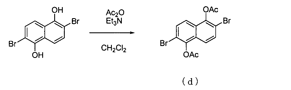

FD-MS(フィールドディソープションマス分析)の測定により目的物であることを確認した。FD-MSの測定結果を以下に示す。
(1)化合物(f)の合成
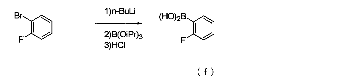

FD-MS(フィールドディソープションマス分析)の測定により目的物であることを確認した。FD-MSの測定結果を以下に示す。
(1)化合物(h)の合成
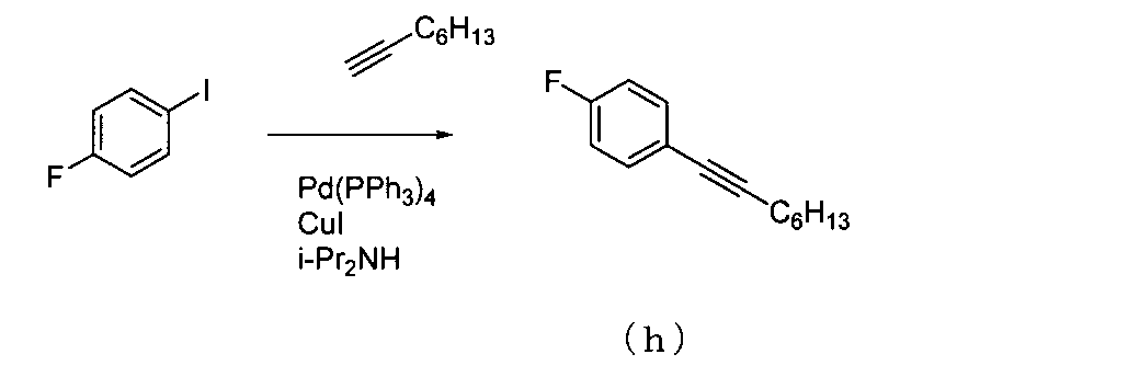
この粗精製物をカラムクロマトグラフィー(ヘキサン)にて精製し、化合物(h)46.0g(収率 100%)を得た。

FD-MS(フィールドディソープションマス分析)の測定により目的物であることを確認した。FD-MSの測定結果を以下に示す。
有機薄膜トランジスタを以下の手順で作製した。
ガラス基板を中性洗剤、純水、アセトン及びエタノールで各30分超音波洗浄した後、スパッタ法にて金(Au)を40nm成膜してゲート電極を作製した。次いで、この基板を熱CVD装置の成膜部にセットした。
一方、原料の蒸発部には、絶縁体層の原料のポリパラキシレン誘導体[ポリパラ塩化キシレン(Parylene)](商品名;diX-C,第三化成社製)250mgをシャーレに入れて設置した。熱CVD装置を真空ポンプで真空に引き、5Paまで減圧した後、蒸発部を180℃、重合部を680℃まで加熱して2時間放置しゲート電極上に厚さ1μmの絶縁体層を形成した。
ID=(W/2L)・Cμ・(VG-VT)2 (A)
式中、IDはソース-ドレイン間電流、Wはチャンネル幅、Lはチャンネル長、Cはゲート絶縁体層の単位面積あたりの電気容量、VTはゲート閾値電圧、VGはゲート電圧である。
実施例4と同様に基板の洗浄,ゲート電極成膜,絶縁体層を成膜した。次いで、化合物(A-8)をトルエンに0.4質量%溶解させ、前記絶縁体層まで成膜した基板の上にスピンコーター(ミカサ社製:1H‐D7)で成膜し、窒素雰囲気下80℃にて乾燥させ有機半導体層として成膜した。次いで、真空蒸着装置で金属マスクを通して金(Au)を50nmの膜厚で成膜することにより、互いに接しないソース及びドレイン電極形成し、有機薄膜トランジスタを作製した。得られた有機薄膜トランジスタについて、実施例4と同様にして、-70Vのゲート電圧VGにてp型駆動させた。ソース-ドレイン電極間の電流のオン/オフを測定し、正孔の電界効果移動度μを算出した結果を表1に示す。
有機半導体層の材料として、化合物(A-8)の代わりに化合物(A-23)を用いた以外は、実施例5と同様にして有機薄膜トランジスタを作製した。得られた有機薄膜トランジスタについて、実施例4と同様にして、-70Vのゲート電圧VGにてp型駆動させた。ソース-ドレイン電極間の電流のオン/オフ比を測定し、正孔の電界効果移動度μを算出した結果を表1に示す。
有機薄膜トランジスタを以下の手順で作製した。まず、Si基板(P型比抵抗1Ωcmゲート電極兼用)を熱酸化法にて表面を酸化させ、基板上300nmの熱酸化膜を作製して絶縁体層とした。さらに基板の一方に成膜したSiO2膜をドライエッチングにて完全に除去した後、さらにその上に金(Au)を100nmスパッタにて成膜し取り出し電極とした。この基板を、中性洗剤、純水、アセトン及びエタノールで各30分超音波洗浄し、さらにオゾン洗浄を行った。

(1)化合物(l)の合成

この粗精製物をカラムクロマトグラフィーにて精製し、化合物(l)17.8g(収率82%)を得た。

この粗精製物をカラムクロマトグラフィーにて精製し、化合物(m)18.3g(収率80%)を得た。
化合物(c)の代わりに化合物(m)を用いた他は、実施例1と同様にして化合物(A-4)を合成した。
FD-MSの測定により目的物であることを確認した。FD-MSの測定結果を以下に示す。
実施例1、又は実施例7と同様にして、それぞれに対応するボロン酸を合成し、当該ボロン酸を用いて、実施例1と同様にして化合物(A-5)、(A-6)、(A-7)、(A-9)、(A-10)、(A-11)、(A-12)を合成した。
FD-MSの測定により目的物であることを確認した。FD-MSの測定結果を以下に示す。
FD-MS,calcd for C32H32O2=448,found,m/z=448(M+,100)
化合物(A-6)
FD-MS,calcd for C34H36O2=476,found,m/z=476(M+,100)
化合物(A-7)
FD-MS,calcd for C36H40O2=504,found,m/z=504(M+,100)
化合物(A-9)
FD-MS,calcd for C40H48O2=560,found,m/z=560(M+,100)
化合物(A-10)
FD-MS,calcd for C42H52O2=588,found,m/z=588(M+,100)
化合物(A-11)
FD-MS,calcd for C44H56O2=616,found,m/z=616(M+,100)
化合物(A-12)
FD-MS,calcd for C46H60O2=644,found,m/z=644(M+,100)
化合物(n)の合成

この粗精製物をカラムクロマトグラフィーと減圧蒸留にて精製し、化合物(n)6.9g(収率50%)を得た。
FD-MSの測定により目的物であることを確認した。FD-MSの測定結果を以下に示す。
実施例3、又は実施例15と同様にしてそれぞれに対応するボロン酸を合成し、当該以ボロン酸を用いて、実施例3と同様にして化合物(A-20)、(A-21)、(A-22)、(A-24)、(A-25)、(A-26)、(A-27)を合成した。
FD-MSの測定により目的物であることを確認した。FD-MSの測定結果を以下に示す。
FD-MS,calcd for C32H32O2=448,found,m/z=448(M+,100)
化合物(A-21)
FD-MS,calcd for C34H36O2=476,found,m/z=476(M+,100)
化合物(A-22)
FD-MS,calcd for C36H40O2=504,found,m/z=504(M+,100)
化合物(A-24)
FD-MS,calcd for C40H48O2=560,found,m/z=560(M+,100)
化合物(A-25)
FD-MS,calcd for C42H52O2=588,found,m/z=588(M+,100)
化合物(A-26)
FD-MS,calcd for C44H56O2=616,found,m/z=616(M+,100)
化合物(A-27)
FD-MS,calcd for C46H60O2=644,found,m/z=644(M+,100)
化合物(o)の合成

この粗精製物をカラムクロマトグラフィーにて精製し、化合物(o)18.2g(収率90%)を得た。
FD-MSの測定により目的物であることを確認した。FD-MSの測定結果を以下に示す。
(1)化合物(p)の合成


この粗精製物をカラムクロマトグラフィーにて精製し、化合物(q)43.1g(収率92%)を得た。

この粗精製物をカラムクロマトグラフィーにて精製し、化合物(r)18.1g(収率83%)を得た。
FD-MSの測定により目的物であることを確認した。FD-MSの測定結果を以下に示す。
有機半導体層の材料として、化合物(A-8)の代わりに化合物(A-4)、(A-5)、(A-6)、(A-7)、(A-9)、(A-10)、(A-11)、(A-12)、(A-19)、(A-20)、(A-21)、(A-22)、(A-48)、(A-50)をそれぞれ用いた他は、実施例5と同様にして有機薄膜トランジスタを作製した。得られた有機薄膜トランジスタについて、実施例4と同様にして、-70Vのゲート電圧VGにてp型駆動させた。ソース-ドレイン電極間の電流のオン/オフ比を測定し、正孔の電界効果移動度μを算出した結果を表2に示す。
この明細書に記載の文献の内容を全てここに援用する
Claims (8)
- 下記式(1)で表わされる有機薄膜トランジスタ用化合物。

R1~R13は、それぞれ、水素原子、ハロゲン原子、炭素数1~30のアルキル基、炭素数1~30のハロアルキル基、炭素数1~30のアルコキシ基、炭素数1~30のハロアルコキシ基、炭素数1~30のアルキルチオ基、炭素数1~30のハロアルキルチオ基、炭素数1~30のアルキルアミノ基、炭素数2~60のジアルキルアミノ基(アルキル基は互いに結合して窒素原子を含む環構造を形成してもよい)、炭素数1~30のアルキルスルホニル基、炭素数1~30のハロアルキルスルホニル基、炭素数3~60のアリール基、炭素数3~20のアルキルシリル基、炭素数5~60のアルキルシリルエチニル基、炭素数3~60のアリールアミノ基、炭素数6~120のジアリールアミノ基又はシアノ基であり、これら各基は置換基を有していてもよい。
X1がともにN-R13で表わされる基である場合、2つのR13は同一でも異なっていてもよい。] - 下記式(2)で表される多環縮環化合物。

R21~R32は、それぞれ、水素原子、ハロゲン原子、炭素数1~30のアルキル基、炭素数1~30のハロアルキル基、炭素数1~30のアルコキシ基、炭素数1~30のハロアルコキシ基、炭素数1~30のアルキルチオ基、炭素数1~30のハロアルキルチオ基、炭素数1~30のアルキルアミノ基、炭素数2~60のジアルキルアミノ基(アルキル基は互いに結合して窒素原子を含む環構造を形成してもよい)、炭素数1~30のアルキルスルホニル基、炭素数1~30のハロアルキルスルホニル基、炭素数3~60のアリール基、炭素数3~20のアルキルシリル基、炭素数5~60のアルキルシリルエチニル基、炭素数3~60のアリールアミノ基、炭素数6~120のジアリールアミノ基又はシアノ基であり、これら各基は置換基を有していてもよい。
R33は、ハロゲン原子、炭素数1~30のアルキル基、炭素数1~30のハロアルキル基、炭素数1~30のアルコキシ基、炭素数1~30のハロアルコキシ基、炭素数1~30のアルキルチオ基、炭素数1~30のハロアルキルチオ基、炭素数1~30のアルキルアミノ基、炭素数2~60のジアルキルアミノ基(アルキル基は互いに結合して窒素原子を含む環構造を形成してもよい)、炭素数1~30のアルキルスルホニル基、炭素数1~30のハロアルキルスルホニル基、炭素数3~60のアリール基、炭素数3~20のアルキルシリル基、炭素数5~60のアルキルシリルエチニル基、炭素数3~60のアリールアミノ基、炭素数6~120のジアリールアミノ基又はシアノ基であり、これら各基は置換基を有していてもよい。
X2がともにN-R33で表わされる基である場合、2つのR33は同一でも異なっていてもよい。] - 請求項1又は2に記載の式(1)又は式(2)に示す化合物を含むことを特徴とする有機薄膜トランジスタ用材料。
- 少なくとも基板上にゲート電極、ソース電極及びドレイン電極の3端子、絶縁体層並びに有機半導体層が設けられ、ソース-ドレイン間電流をゲート電極に電圧を印加することによって制御する有機薄膜トランジスタにおいて、前記有機半導体層が、請求項1又は2に記載の式(1)又は式(2)に示す化合物を含む有機薄膜トランジスタ。
- ソース-ドレイン間を流れる電流を利用して発光し、ゲート電極に電圧を印加することによって発光を制御する請求項4に記載の有機薄膜トランジスタ。
- ソース電極及びドレイン電極の一方が仕事関数4.2eV以上の物質からなり、他方が仕事関数4.3eV以下の物質からなる請求項5に記載の有機薄膜トランジスタ。
- ソース及びドレイン電極と有機半導体層の間にバッファ層を有する請求項4~6のいずれかに記載の有機薄膜トランジスタ。
- 請求項4~7のいずれかに記載の有機薄膜トランジスタを備えた装置。
Priority Applications (3)
| Application Number | Priority Date | Filing Date | Title |
|---|---|---|---|
| CN2010800563247A CN102666549A (zh) | 2009-12-14 | 2010-12-13 | 多环稠环化合物以及使用该多环稠环化合物的有机薄膜晶体管 |
| US13/514,453 US8946688B2 (en) | 2009-12-14 | 2010-12-13 | Polycyclic ring-fused compound and organic thin film transistor utilizing the same |
| JP2011545954A JP5666474B2 (ja) | 2009-12-14 | 2010-12-13 | 多環縮環化合物、及び、それを用いた有機薄膜トランジスタ |
Applications Claiming Priority (2)
| Application Number | Priority Date | Filing Date | Title |
|---|---|---|---|
| JP2009-283280 | 2009-12-14 | ||
| JP2009283280 | 2009-12-14 |
Publications (1)
| Publication Number | Publication Date |
|---|---|
| WO2011074232A1 true WO2011074232A1 (ja) | 2011-06-23 |
Family
ID=44167004
Family Applications (1)
| Application Number | Title | Priority Date | Filing Date |
|---|---|---|---|
| PCT/JP2010/007220 Ceased WO2011074232A1 (ja) | 2009-12-14 | 2010-12-13 | 多環縮環化合物、及び、それを用いた有機薄膜トランジスタ |
Country Status (5)
| Country | Link |
|---|---|
| US (1) | US8946688B2 (ja) |
| JP (1) | JP5666474B2 (ja) |
| CN (1) | CN102666549A (ja) |
| TW (1) | TW201129545A (ja) |
| WO (1) | WO2011074232A1 (ja) |
Cited By (11)
| Publication number | Priority date | Publication date | Assignee | Title |
|---|---|---|---|---|
| JP2013232521A (ja) * | 2012-04-27 | 2013-11-14 | Udc Ireland Ltd | 有機電界発光素子、有機電界発光素子用材料並びに該有機電界発光素子を用いた発光装置、表示装置及び照明装置 |
| JP2014024844A (ja) * | 2012-07-25 | 2014-02-06 | Samsung Display Co Ltd | ヘテロ環化合物、有機発光素子及び有機発光表示装置 |
| JP2014159390A (ja) * | 2013-02-20 | 2014-09-04 | Nippon Kagaku Kogyosho:Kk | 新規な光重合開始剤及びこれらを用いた感光性樹脂組成物 |
| WO2014148614A1 (ja) * | 2013-03-22 | 2014-09-25 | 富士フイルム株式会社 | 有機薄膜トランジスタ |
| WO2014156773A1 (ja) * | 2013-03-29 | 2014-10-02 | 新日鉄住金化学株式会社 | 芳香族複素環化合物、その製造方法、有機半導体材料及び有機半導体デバイス |
| JP2015513795A (ja) * | 2012-02-27 | 2015-05-14 | エ・ティ・チ・エッセ・エッレ・エッレ | 分散した発光を有する有機発光電界効果アンバイポーラトランジスタ |
| US20150218184A1 (en) * | 2012-10-15 | 2015-08-06 | Fujifilm Corporation | Organic thin film transistor, organic semiconductor thin film, and organic semiconductor material |
| JP2015199716A (ja) * | 2014-03-31 | 2015-11-12 | 日本化薬株式会社 | 多環縮環化合物、有機半導体材料、有機半導体デバイス及び有機トランジスタ |
| WO2016051977A1 (ja) * | 2014-09-29 | 2016-04-07 | 新日鉄住金化学株式会社 | 有機電界発光素子用材料及びこれを用いた有機電界発光素子 |
| US9660103B2 (en) | 2013-06-28 | 2017-05-23 | Kobe Steel, Ltd. | Thin film transistor and method for manufacturing same |
| JP2022179515A (ja) * | 2017-04-07 | 2022-12-02 | 株式会社半導体エネルギー研究所 | 有機化合物 |
Families Citing this family (6)
| Publication number | Priority date | Publication date | Assignee | Title |
|---|---|---|---|---|
| JP2014209522A (ja) * | 2013-04-16 | 2014-11-06 | 富士通株式会社 | 半導体装置及びその製造方法 |
| KR102263057B1 (ko) | 2014-05-07 | 2021-06-09 | 삼성전자주식회사 | 축합환 화합물 및 이를 포함한 유기 발광 소자 |
| JP6116018B2 (ja) | 2015-01-29 | 2017-04-19 | 国立大学法人 東京大学 | 有機半導体素子 |
| US11239426B2 (en) | 2016-11-23 | 2022-02-01 | Lg Chem, Ltd. | Electroactive compounds |
| WO2020019119A1 (zh) * | 2018-07-23 | 2020-01-30 | 湖北中烟工业有限责任公司 | 一种电子浆料组合物及其制备方法和用途 |
| CN109880635B (zh) * | 2019-03-19 | 2021-02-02 | 石家庄晶奥量新材料有限公司 | 含有二苯并呋喃并含氧杂环类液晶化合物和组合物及应用 |
Citations (2)
| Publication number | Priority date | Publication date | Assignee | Title |
|---|---|---|---|---|
| US20040131880A1 (en) * | 2002-12-31 | 2004-07-08 | Eastman Kodak Company | Complex fluorene-containing compounds |
| JP2009267134A (ja) * | 2008-04-25 | 2009-11-12 | Mitsui Chemicals Inc | 有機トランジスタ |
Family Cites Families (9)
| Publication number | Priority date | Publication date | Assignee | Title |
|---|---|---|---|---|
| US5936259A (en) | 1997-10-16 | 1999-08-10 | Lucent Technologies Inc. | Thin film transistor and organic semiconductor material thereof |
| US6768132B2 (en) * | 2002-03-07 | 2004-07-27 | 3M Innovative Properties Company | Surface modified organic thin film transistors |
| WO2006046521A1 (ja) * | 2004-10-25 | 2006-05-04 | Matsushita Electric Industrial Co., Ltd. | 電子デバイスおよびその製造方法、ならびにそれを用いた電子機器 |
| JP5410760B2 (ja) * | 2005-12-12 | 2014-02-05 | チバ ホールディング インコーポレーテッド | 半導体素子、化合物、半導体素子の半導体層及び薄膜トランジスタ素子を作製する方法 |
| WO2008012250A1 (en) * | 2006-07-28 | 2008-01-31 | Ciba Holding Inc. | Novel polymers |
| TWI428331B (zh) * | 2007-01-26 | 2014-03-01 | 東麗股份有限公司 | 有機半導體複合物、有機電晶體材料、及有機場效型電晶體 |
| US20100187514A1 (en) | 2007-06-21 | 2010-07-29 | Yuki Nakano | Organic thin film transistor and organic thin film light- emitting transistor |
| EP2383273A4 (en) * | 2009-01-22 | 2012-06-27 | Sumitomo Chemical Co | AROMATIC COMPOUND AND METHOD FOR THE PRODUCTION THEREOF |
| CN102449023B (zh) * | 2009-05-27 | 2015-10-07 | 巴斯夫欧洲公司 | 多环联噻吩 |
-
2010
- 2010-12-13 JP JP2011545954A patent/JP5666474B2/ja not_active Expired - Fee Related
- 2010-12-13 CN CN2010800563247A patent/CN102666549A/zh active Pending
- 2010-12-13 US US13/514,453 patent/US8946688B2/en active Active
- 2010-12-13 WO PCT/JP2010/007220 patent/WO2011074232A1/ja not_active Ceased
- 2010-12-14 TW TW099143821A patent/TW201129545A/zh unknown
Patent Citations (2)
| Publication number | Priority date | Publication date | Assignee | Title |
|---|---|---|---|---|
| US20040131880A1 (en) * | 2002-12-31 | 2004-07-08 | Eastman Kodak Company | Complex fluorene-containing compounds |
| JP2009267134A (ja) * | 2008-04-25 | 2009-11-12 | Mitsui Chemicals Inc | 有機トランジスタ |
Non-Patent Citations (1)
| Title |
|---|
| DUFOUR, F. ET AL.: "Carbazolo[2,1-a]carbazole derivatives via Fischer indole synthesis", JOURNAL OF HETEROCYCLIC CHEMISTRY, vol. 45, no. 1, 2008, pages 161 - 163, XP002610758 * |
Cited By (20)
| Publication number | Priority date | Publication date | Assignee | Title |
|---|---|---|---|---|
| JP2015513795A (ja) * | 2012-02-27 | 2015-05-14 | エ・ティ・チ・エッセ・エッレ・エッレ | 分散した発光を有する有機発光電界効果アンバイポーラトランジスタ |
| JP2013232521A (ja) * | 2012-04-27 | 2013-11-14 | Udc Ireland Ltd | 有機電界発光素子、有機電界発光素子用材料並びに該有機電界発光素子を用いた発光装置、表示装置及び照明装置 |
| JP2014024844A (ja) * | 2012-07-25 | 2014-02-06 | Samsung Display Co Ltd | ヘテロ環化合物、有機発光素子及び有機発光表示装置 |
| TWI594983B (zh) * | 2012-10-15 | 2017-08-11 | 富士軟片股份有限公司 | 有機薄膜電晶體、萘并雙苯并呋喃化合物、非發光性有機半導體元件用塗佈溶液、有機半導體薄膜、有機薄膜電晶體用材料及有機半導體材料 |
| US20150218184A1 (en) * | 2012-10-15 | 2015-08-06 | Fujifilm Corporation | Organic thin film transistor, organic semiconductor thin film, and organic semiconductor material |
| US9447111B2 (en) * | 2012-10-15 | 2016-09-20 | Fujifilm Corporation | Organic thin film transistor, organic semiconductor thin film, and organic semiconductor material |
| JP2014159390A (ja) * | 2013-02-20 | 2014-09-04 | Nippon Kagaku Kogyosho:Kk | 新規な光重合開始剤及びこれらを用いた感光性樹脂組成物 |
| WO2014148614A1 (ja) * | 2013-03-22 | 2014-09-25 | 富士フイルム株式会社 | 有機薄膜トランジスタ |
| JP2014209597A (ja) * | 2013-03-22 | 2014-11-06 | 富士フイルム株式会社 | 有機薄膜トランジスタ、有機半導体薄膜および有機半導体材料 |
| TWI606053B (zh) * | 2013-03-22 | 2017-11-21 | 富士軟片股份有限公司 | 有機薄膜電晶體、化合物、有機半導體薄膜、有機半導體材料、有機薄膜電晶體用材料及有機半導體元件用塗佈溶液 |
| JPWO2014156773A1 (ja) * | 2013-03-29 | 2017-02-16 | 新日鉄住金化学株式会社 | 芳香族複素環化合物、その製造方法、有機半導体材料及び有機半導体デバイス |
| KR20150135792A (ko) | 2013-03-29 | 2015-12-03 | 신닛테츠 수미킨 가가쿠 가부시키가이샤 | 방향족 복소환 화합물, 그 제조방법, 유기 반도체 재료 및 유기 반도체 디바이스 |
| WO2014156773A1 (ja) * | 2013-03-29 | 2014-10-02 | 新日鉄住金化学株式会社 | 芳香族複素環化合物、その製造方法、有機半導体材料及び有機半導体デバイス |
| US10032993B2 (en) | 2013-03-29 | 2018-07-24 | Nippon Steel & Sumikin Chemical Co., Ltd. | Aromatic heterocyclic compound, manufacturing method thereof, organic semiconductor material, and organic semiconductor device |
| US9660103B2 (en) | 2013-06-28 | 2017-05-23 | Kobe Steel, Ltd. | Thin film transistor and method for manufacturing same |
| JP2015199716A (ja) * | 2014-03-31 | 2015-11-12 | 日本化薬株式会社 | 多環縮環化合物、有機半導体材料、有機半導体デバイス及び有機トランジスタ |
| WO2016051977A1 (ja) * | 2014-09-29 | 2016-04-07 | 新日鉄住金化学株式会社 | 有機電界発光素子用材料及びこれを用いた有機電界発光素子 |
| JPWO2016051977A1 (ja) * | 2014-09-29 | 2017-08-31 | 新日鉄住金化学株式会社 | 有機電界発光素子用材料及びこれを用いた有機電界発光素子 |
| JP2022179515A (ja) * | 2017-04-07 | 2022-12-02 | 株式会社半導体エネルギー研究所 | 有機化合物 |
| US12421202B2 (en) | 2017-04-07 | 2025-09-23 | Semiconductor Energy Laboratory Co., Ltd. | Organic compound, light-emitting element, light-emitting device, electronic device, display device and lighting device |
Also Published As
| Publication number | Publication date |
|---|---|
| JPWO2011074232A1 (ja) | 2013-04-25 |
| CN102666549A (zh) | 2012-09-12 |
| US8946688B2 (en) | 2015-02-03 |
| JP5666474B2 (ja) | 2015-02-12 |
| TW201129545A (en) | 2011-09-01 |
| US20120273770A1 (en) | 2012-11-01 |
Similar Documents
| Publication | Publication Date | Title |
|---|---|---|
| JP5666474B2 (ja) | 多環縮環化合物、及び、それを用いた有機薄膜トランジスタ | |
| JP5490005B2 (ja) | 有機薄膜トランジスタ用化合物及びそれを用いた有機薄膜トランジスタ | |
| JP5460599B2 (ja) | 有機薄膜トランジスタ用化合物及びそれを用いた有機薄膜トランジスタ | |
| JPWO2010024388A1 (ja) | 有機薄膜トランジスタ用化合物及びそれを用いた有機薄膜トランジスタ | |
| JPWO2008044695A1 (ja) | 有機薄膜トランジスタ素子及び有機薄膜発光トランジスタ | |
| JPWO2010016511A1 (ja) | 有機薄膜トランジスタ用化合物及びそれを用いた有機薄膜トランジスタ | |
| JPWO2007094361A1 (ja) | 有機薄膜トランジスタ及び有機薄膜発光トランジスタ | |
| JP5299807B2 (ja) | ベンゾジチオフェン誘導体並びにそれを用いた有機薄膜トランジスタ及び有機薄膜発光トランジスタ | |
| JPWO2011074231A1 (ja) | 多環縮環化合物及びそれを用いた有機薄膜トランジスタ | |
| JP5677306B2 (ja) | 有機薄膜トランジスタ | |
| JP5452476B2 (ja) | 有機薄膜トランジスタ用化合物及び有機薄膜トランジスタ | |
| JPWO2008069061A1 (ja) | 有機薄膜トランジスタ及び有機薄膜発光トランジスタ | |
| WO2012090462A1 (ja) | 有機半導体材料、当該材料を含んでなる塗布液、及び有機薄膜トランジスタ | |
| JP5308164B2 (ja) | 有機薄膜トランジスタ及び有機薄膜発光トランジスタ | |
| JPWO2008062841A1 (ja) | 有機薄膜トランジスタ及び有機薄膜発光トランジスタ | |
| JP5528330B2 (ja) | 有機薄膜トランジスタ用化合物及びそれを用いた有機薄膜トランジスタ | |
| JP5452475B2 (ja) | 有機薄膜トランジスタ用化合物及びそれを用いた有機薄膜トランジスタ | |
| JP5329404B2 (ja) | 有機薄膜トランジスタ及び有機薄膜発光トランジスタ | |
| JP2014139143A (ja) | ジチエノフェナントレン化合物、当該化合物を含む有機薄膜トランジスタ用組成物、及び有機薄膜トランジスタ | |
| JP2010275239A (ja) | 新規な縮合芳香環化合物及びそれを用いた有機薄膜トランジスタ | |
| JP5308162B2 (ja) | 有機薄膜トランジスタ及び有機薄膜発光トランジスタ | |
| JP2014019671A (ja) | 芳香族ヘテロ環化合物及びそれを用いた有機薄膜トランジスタ |
Legal Events
| Date | Code | Title | Description |
|---|---|---|---|
| WWE | Wipo information: entry into national phase |
Ref document number: 201080056324.7 Country of ref document: CN |
|
| 121 | Ep: the epo has been informed by wipo that ep was designated in this application |
Ref document number: 10837266 Country of ref document: EP Kind code of ref document: A1 |
|
| WWE | Wipo information: entry into national phase |
Ref document number: 2011545954 Country of ref document: JP |
|
| NENP | Non-entry into the national phase |
Ref country code: DE |
|
| WWE | Wipo information: entry into national phase |
Ref document number: 13514453 Country of ref document: US |
|
| 122 | Ep: pct application non-entry in european phase |
Ref document number: 10837266 Country of ref document: EP Kind code of ref document: A1 |