WO2011064997A1 - 半導体基板及び半導体基板の製造方法 - Google Patents
半導体基板及び半導体基板の製造方法 Download PDFInfo
- Publication number
- WO2011064997A1 WO2011064997A1 PCT/JP2010/006871 JP2010006871W WO2011064997A1 WO 2011064997 A1 WO2011064997 A1 WO 2011064997A1 JP 2010006871 W JP2010006871 W JP 2010006871W WO 2011064997 A1 WO2011064997 A1 WO 2011064997A1
- Authority
- WO
- WIPO (PCT)
- Prior art keywords
- alignment mark
- base substrate
- semiconductor
- substrate
- crystal
- Prior art date
- Legal status (The legal status is an assumption and is not a legal conclusion. Google has not performed a legal analysis and makes no representation as to the accuracy of the status listed.)
- Ceased
Links
Images




Classifications
-
- G—PHYSICS
- G03—PHOTOGRAPHY; CINEMATOGRAPHY; ANALOGOUS TECHNIQUES USING WAVES OTHER THAN OPTICAL WAVES; ELECTROGRAPHY; HOLOGRAPHY
- G03F—PHOTOMECHANICAL PRODUCTION OF TEXTURED OR PATTERNED SURFACES, e.g. FOR PRINTING, FOR PROCESSING OF SEMICONDUCTOR DEVICES; MATERIALS THEREFOR; ORIGINALS THEREFOR; APPARATUS SPECIALLY ADAPTED THEREFOR
- G03F9/00—Registration or positioning of originals, masks, frames, photographic sheets or textured or patterned surfaces, e.g. automatically
- G03F9/70—Registration or positioning of originals, masks, frames, photographic sheets or textured or patterned surfaces, e.g. automatically for microlithography
- G03F9/7073—Alignment marks and their environment
- G03F9/7084—Position of mark on substrate, i.e. position in (x, y, z) of mark, e.g. buried or resist covered mark, mark on rearside, at the substrate edge, in the circuit area, latent image mark, marks in plural levels
-
- H—ELECTRICITY
- H10—SEMICONDUCTOR DEVICES; ELECTRIC SOLID-STATE DEVICES NOT OTHERWISE PROVIDED FOR
- H10P—GENERIC PROCESSES OR APPARATUS FOR THE MANUFACTURE OR TREATMENT OF DEVICES COVERED BY CLASS H10
- H10P14/00—Formation of materials, e.g. in the shape of layers or pillars
- H10P14/20—Formation of materials, e.g. in the shape of layers or pillars of semiconductor materials
-
- G—PHYSICS
- G03—PHOTOGRAPHY; CINEMATOGRAPHY; ANALOGOUS TECHNIQUES USING WAVES OTHER THAN OPTICAL WAVES; ELECTROGRAPHY; HOLOGRAPHY
- G03F—PHOTOMECHANICAL PRODUCTION OF TEXTURED OR PATTERNED SURFACES, e.g. FOR PRINTING, FOR PROCESSING OF SEMICONDUCTOR DEVICES; MATERIALS THEREFOR; ORIGINALS THEREFOR; APPARATUS SPECIALLY ADAPTED THEREFOR
- G03F9/00—Registration or positioning of originals, masks, frames, photographic sheets or textured or patterned surfaces, e.g. automatically
- G03F9/70—Registration or positioning of originals, masks, frames, photographic sheets or textured or patterned surfaces, e.g. automatically for microlithography
- G03F9/7073—Alignment marks and their environment
- G03F9/708—Mark formation
-
- H—ELECTRICITY
- H10—SEMICONDUCTOR DEVICES; ELECTRIC SOLID-STATE DEVICES NOT OTHERWISE PROVIDED FOR
- H10P—GENERIC PROCESSES OR APPARATUS FOR THE MANUFACTURE OR TREATMENT OF DEVICES COVERED BY CLASS H10
- H10P14/00—Formation of materials, e.g. in the shape of layers or pillars
- H10P14/20—Formation of materials, e.g. in the shape of layers or pillars of semiconductor materials
- H10P14/27—Formation of materials, e.g. in the shape of layers or pillars of semiconductor materials using selective deposition, e.g. simultaneous growth of monocrystalline and non-monocrystalline semiconductor materials
- H10P14/271—Formation of materials, e.g. in the shape of layers or pillars of semiconductor materials using selective deposition, e.g. simultaneous growth of monocrystalline and non-monocrystalline semiconductor materials characterised by the preparation of substrate for selective deposition
- H10P14/272—Formation of materials, e.g. in the shape of layers or pillars of semiconductor materials using selective deposition, e.g. simultaneous growth of monocrystalline and non-monocrystalline semiconductor materials characterised by the preparation of substrate for selective deposition using mask materials other than SiO2 or SiN
-
- H—ELECTRICITY
- H10—SEMICONDUCTOR DEVICES; ELECTRIC SOLID-STATE DEVICES NOT OTHERWISE PROVIDED FOR
- H10P—GENERIC PROCESSES OR APPARATUS FOR THE MANUFACTURE OR TREATMENT OF DEVICES COVERED BY CLASS H10
- H10P14/00—Formation of materials, e.g. in the shape of layers or pillars
- H10P14/20—Formation of materials, e.g. in the shape of layers or pillars of semiconductor materials
- H10P14/29—Formation of materials, e.g. in the shape of layers or pillars of semiconductor materials characterised by the substrates
- H10P14/2901—Materials
- H10P14/2902—Materials being Group IVA materials
- H10P14/2905—Silicon, silicon germanium or germanium
-
- H—ELECTRICITY
- H10—SEMICONDUCTOR DEVICES; ELECTRIC SOLID-STATE DEVICES NOT OTHERWISE PROVIDED FOR
- H10P—GENERIC PROCESSES OR APPARATUS FOR THE MANUFACTURE OR TREATMENT OF DEVICES COVERED BY CLASS H10
- H10P14/00—Formation of materials, e.g. in the shape of layers or pillars
- H10P14/20—Formation of materials, e.g. in the shape of layers or pillars of semiconductor materials
- H10P14/29—Formation of materials, e.g. in the shape of layers or pillars of semiconductor materials characterised by the substrates
- H10P14/2926—Crystal orientations
-
- H—ELECTRICITY
- H10—SEMICONDUCTOR DEVICES; ELECTRIC SOLID-STATE DEVICES NOT OTHERWISE PROVIDED FOR
- H10P—GENERIC PROCESSES OR APPARATUS FOR THE MANUFACTURE OR TREATMENT OF DEVICES COVERED BY CLASS H10
- H10P14/00—Formation of materials, e.g. in the shape of layers or pillars
- H10P14/20—Formation of materials, e.g. in the shape of layers or pillars of semiconductor materials
- H10P14/32—Formation of materials, e.g. in the shape of layers or pillars of semiconductor materials characterised by intermediate layers between substrates and deposited layers
- H10P14/3202—Materials thereof
-
- H—ELECTRICITY
- H10—SEMICONDUCTOR DEVICES; ELECTRIC SOLID-STATE DEVICES NOT OTHERWISE PROVIDED FOR
- H10P—GENERIC PROCESSES OR APPARATUS FOR THE MANUFACTURE OR TREATMENT OF DEVICES COVERED BY CLASS H10
- H10P14/00—Formation of materials, e.g. in the shape of layers or pillars
- H10P14/20—Formation of materials, e.g. in the shape of layers or pillars of semiconductor materials
- H10P14/32—Formation of materials, e.g. in the shape of layers or pillars of semiconductor materials characterised by intermediate layers between substrates and deposited layers
- H10P14/3202—Materials thereof
- H10P14/3204—Materials thereof being Group IVA semiconducting materials
-
- H—ELECTRICITY
- H10—SEMICONDUCTOR DEVICES; ELECTRIC SOLID-STATE DEVICES NOT OTHERWISE PROVIDED FOR
- H10P—GENERIC PROCESSES OR APPARATUS FOR THE MANUFACTURE OR TREATMENT OF DEVICES COVERED BY CLASS H10
- H10P14/00—Formation of materials, e.g. in the shape of layers or pillars
- H10P14/20—Formation of materials, e.g. in the shape of layers or pillars of semiconductor materials
- H10P14/32—Formation of materials, e.g. in the shape of layers or pillars of semiconductor materials characterised by intermediate layers between substrates and deposited layers
- H10P14/3202—Materials thereof
- H10P14/3214—Materials thereof being Group IIIA-VA semiconductors
- H10P14/3216—Nitrides
-
- H—ELECTRICITY
- H10—SEMICONDUCTOR DEVICES; ELECTRIC SOLID-STATE DEVICES NOT OTHERWISE PROVIDED FOR
- H10P—GENERIC PROCESSES OR APPARATUS FOR THE MANUFACTURE OR TREATMENT OF DEVICES COVERED BY CLASS H10
- H10P14/00—Formation of materials, e.g. in the shape of layers or pillars
- H10P14/20—Formation of materials, e.g. in the shape of layers or pillars of semiconductor materials
- H10P14/32—Formation of materials, e.g. in the shape of layers or pillars of semiconductor materials characterised by intermediate layers between substrates and deposited layers
- H10P14/3242—Structure
- H10P14/3244—Layer structure
- H10P14/3248—Layer structure consisting of two layers
-
- H—ELECTRICITY
- H10—SEMICONDUCTOR DEVICES; ELECTRIC SOLID-STATE DEVICES NOT OTHERWISE PROVIDED FOR
- H10P—GENERIC PROCESSES OR APPARATUS FOR THE MANUFACTURE OR TREATMENT OF DEVICES COVERED BY CLASS H10
- H10P14/00—Formation of materials, e.g. in the shape of layers or pillars
- H10P14/20—Formation of materials, e.g. in the shape of layers or pillars of semiconductor materials
- H10P14/34—Deposited materials, e.g. layers
- H10P14/3402—Deposited materials, e.g. layers characterised by the chemical composition
-
- H—ELECTRICITY
- H10—SEMICONDUCTOR DEVICES; ELECTRIC SOLID-STATE DEVICES NOT OTHERWISE PROVIDED FOR
- H10P—GENERIC PROCESSES OR APPARATUS FOR THE MANUFACTURE OR TREATMENT OF DEVICES COVERED BY CLASS H10
- H10P14/00—Formation of materials, e.g. in the shape of layers or pillars
- H10P14/20—Formation of materials, e.g. in the shape of layers or pillars of semiconductor materials
- H10P14/34—Deposited materials, e.g. layers
- H10P14/3402—Deposited materials, e.g. layers characterised by the chemical composition
- H10P14/3414—Deposited materials, e.g. layers characterised by the chemical composition being group IIIA-VIA materials
- H10P14/3416—Nitrides
Definitions
- the present invention relates to a semiconductor substrate and a method for manufacturing the semiconductor substrate.
- Non-Patent Document 1 A technique for selectively growing GaN on an AlN buffer layer formed on a Si substrate is known (see, for example, Non-Patent Document 1).
- a technique for growing a semiconductor crystal using alignment marks formed on a semiconductor substrate is also known (see, for example, Patent Document 1).
- Non-Patent Document 1 S. Haffouz, et. Al., Journal of crystal growth, 311 (2009) 2087-2090
- Patent Document 1 Japanese Patent Application Laid-Open No. 10-64781
- a functional crystal is formed on the entire surface of the base substrate.
- an alignment mark is formed on the functional crystal using a notch or an orientation flat provided in advance in the base substrate as a mechanical guide.
- functional members such as electrodes and wiring metals are formed on the functional crystal.
- the functional crystal is partially formed instead of the entire surface of the base substrate using the notch or the orientation flat as a mechanical guide, and then the alignment mark is formed, the following problems occur.
- the notch or orientation flat is used as a mechanical guide, the alignment accuracy is low, so that the functional crystal cannot be formed in a systematic alignment with respect to the base substrate.
- alignment marks cannot be formed on the base substrate or on the functional crystal with high accuracy. Therefore, the functional member formed by being aligned with the alignment mark cannot be accurately aligned with the functional crystal. This problem becomes more prominent as the size of the functional crystal decreases.
- the size of the deviation between the position of the alignment mark and the position of the functional crystal is measured, and photolithography is performed with the position corrected based on this measured value.
- functional members such as electrodes and metal wirings can be arranged on the functional crystal with high positional accuracy.
- this method brings about a decrease in productivity and a high cost due to an increase in the number of processes.
- a large number of semiconductor wafers are automatically processed continuously according to a takt time of about several tens of seconds (the time required for one work time), so the position correction value is measured for each substrate.
- the process which corrects the position which forms a functional member according to it leads to the remarkable fall of productivity and high cost.
- the semiconductor crystal when a semiconductor crystal is grown on the semiconductor substrate, the semiconductor crystal grows also in the alignment mark, so that it is difficult to recognize the boundary line (edge) of the alignment mark. As a result, it becomes difficult to detect the alignment mark with high accuracy. Therefore, when a functional member such as an electrode or a metal wiring is arranged on the semiconductor crystal, it is necessary to remove the semiconductor crystal in the alignment mark. there were. When the semiconductor crystal in the alignment mark is not removed, it is necessary to form a new alignment mark.
- a crystal is formed in the region including the alignment mark on the base substrate.
- the base substrate is exposed to a region where the alignment mark is not provided in the inhibition layer based on the step of forming the inhibition layer that inhibits growth and the information indicating the position where the opening should be formed based on the position of the alignment mark.
- a method for manufacturing a semiconductor substrate comprising: forming an opening to be formed; and growing a semiconductor crystal in the opening.
- the manufacturing method may further include a step of forming at least one of an electrode and a metal wiring on the semiconductor crystal with reference to the position of the alignment mark.
- a plurality of openings may be formed in a region where no alignment mark is provided. In the step of forming openings, a plurality of openings may be formed based on information indicating positions where a plurality of openings should be formed with reference to the position of the alignment mark.
- the semiconductor crystal is grown in each of the plurality of openings.
- the manufacturing method further includes a functional member forming step of forming a functional member including at least one of an electrode and a metal wiring above each semiconductor crystal in the plurality of openings on the basis of the position of the alignment mark. May be.
- the functional member formation stage for example, the functional member is formed by lithography using the position of the alignment mark as a reference.
- the base substrate used in the manufacturing method is, for example, a substrate whose surface is a silicon crystal, a substrate whose surface is a germanium crystal, or a group 3-5 compound semiconductor substrate.
- a group 3-5 compound semiconductor crystal or a group 2-6 compound semiconductor crystal is grown.
- the step of growing the semiconductor crystal includes the composition of C x1 Si y1 Ge z1 Sn 1-x1-y1-z1 (0 ⁇ x1 ⁇ 1, 0 ⁇ y1 ⁇ 1, 0 ⁇ z1 ⁇ 1, and 0 ⁇ x1 + y1 + z1 ⁇ 1).
- the inhibition layer formed by the manufacturing method includes, for example, any of silicon oxide, silicon nitride, silicon oxynitride, or aluminum oxide.
- the alignment mark is formed on the base substrate, for example, by etching the base substrate.
- the alignment mark may be formed on the base substrate by forming at least one metal selected from the group consisting of tantalum, niobium, nickel, tungsten, and titanium on the base substrate.
- a semiconductor substrate is provided that includes a first inhibition layer that inhibits crystal growth, a second inhibition layer that is provided on the alignment mark and inhibits crystal growth, and a semiconductor crystal that has grown in the opening.
- the first inhibition layer may have a plurality of openings, and the semiconductor substrate may include a semiconductor crystal grown in each of the plurality of openings.
- the thickness of the base substrate at the position of the alignment mark is different from the thickness of the base substrate in the region of the base substrate other than the position of the alignment mark, and the back surface is the surface opposite to the surface in contact with the first inhibition layer of the base substrate.
- the distance from the back surface to the surface opposite to the surface near the base substrate of the first inhibition layer is different from the distance from the back surface to the surface opposite to the surface near the base substrate of the second inhibition layer.
- the thickness of the base substrate at the position of the alignment mark is smaller than the thickness of the base substrate in the region of the base substrate other than the position of the alignment mark, and is first from the back surface that is the surface opposite to the surface in contact with the first inhibition layer of the base substrate.
- the distance from the back surface to the surface opposite to the surface near the base substrate of the inhibition layer may be larger than the distance from the back surface to the surface opposite to the surface near the base substrate of the second inhibition layer.
- the thickness of the base substrate at the position of the alignment mark is larger than the thickness of the base substrate in the region of the base substrate other than the position of the alignment mark, and is first from the back surface that is the surface opposite to the surface in contact with the first inhibition layer of the base substrate.
- the distance from the back surface to the surface opposite to the surface near the base substrate of the inhibition layer may be smaller than the distance from the back surface to the surface opposite to the surface near the base substrate of the second inhibition layer.
- FIG. 1 is a plan view of a semiconductor substrate 100.
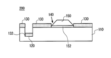
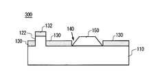
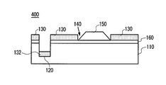
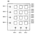
- FIG. It is sectional drawing of the semiconductor substrate 200 which concerns on this embodiment. It is sectional drawing of the semiconductor substrate 300 which concerns on other embodiment. It is sectional drawing of the semiconductor substrate 400 which concerns on other embodiment. It is a top view of semiconductor substrate 500 concerning other embodiments.
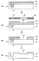
- a method for manufacturing the semiconductor substrate 200 will be described.
- a method for manufacturing the semiconductor substrate 200 will be described.
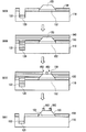
- a method for manufacturing the semiconductor substrate 200 will be described.
- FIG. The shape of the alignment mark 720 formed on the semiconductor substrate 700 is shown. It is sectional drawing of the manufactured semiconductor substrate 900.
- FIG. 1 is a plan view of a semiconductor substrate 100.
- FIG. It is sectional drawing of the semiconductor substrate 200 which concerns on this embodiment. It is sectional drawing of the semiconductor substrate 300 which concerns on other embodiment.
- It is sectional drawing of the semiconductor substrate 400 which concerns on other embodiment.
- FIG. 1A is a cross-sectional view of a semiconductor substrate 100 according to the present embodiment.
- FIG. 1B is a plan view of the semiconductor substrate 100.
- 1A is a cross-sectional view taken along line AA in FIG. 1B.
- the semiconductor substrate 100 includes a base substrate 110, an inhibition layer 130, an inhibition layer 132, and a semiconductor crystal 150.
- An alignment mark 120 is formed on the base substrate 110.
- the alignment mark 120 is formed, for example, by etching a partial region of the base substrate 110.
- the base substrate 110 is a substrate whose surface is a silicon crystal, a substrate whose surface is a germanium crystal, or a group 3-5 compound semiconductor substrate.
- the substrate whose surface is made of silicon crystal means that the substrate has a region where the surface of the substrate is made of silicon crystal.
- Examples of the substrate whose surface is a silicon crystal include an Si substrate (Si wafer) and an SOI (silicon-on-insulator) substrate whose entire substrate is a silicon crystal.
- the substrate whose surface is made of germanium crystal means that the substrate has a region where the surface of the substrate is made of germanium crystal.
- Examples of the substrate whose surface is a germanium crystal include a Ge substrate (Ge wafer) and a GOI (germanium-on-insulator) substrate whose entire substrate is a germanium crystal.
- the group 3-5 compound semiconductor substrate is a substrate made of a group 3-5 compound semiconductor.
- An example of the group 3-5 compound semiconductor substrate is a GaAs substrate.
- the main surface on the side in contact with the inhibition layer 130 among the surfaces of the base substrate 110 is, for example, the (100) plane, the (110) plane, the (111) plane, ( The plane is equivalent to the (100) plane, the plane equivalent to the (110) plane, or the plane equivalent to the (111) plane.
- the main surface of the base substrate 110 may be slightly inclined from the crystallographic plane orientation. That is, the base substrate 110 may have an off angle.
- the inhibition layer 130 is provided in a region other than the region where the alignment mark 120 is formed on the base substrate 110.
- the inhibition layer 130 has an opening 140 that exposes the base substrate 110.
- the opening 140 is formed, for example, by etching a partial region of the inhibition layer 130.
- the inhibition layer 130 inhibits the crystal growth of the semiconductor crystal 150. For example, as shown in FIG. 1A, the semiconductor crystal 150 grows in the opening 140 and does not grow on the surface of the inhibition layer 130.
- the inhibition layer 132 is provided on the alignment mark 120 and inhibits crystal growth. Even on the surface of the inhibition layer 132, the semiconductor crystal 150 does not grow.
- the inhibition layer 130 and the inhibition layer 132 include silicon oxide, silicon nitride, silicon oxynitride, or aluminum oxide.
- the inhibition layer 130 and the inhibition layer 132 may be formed by stacking any of silicon oxide, silicon nitride, silicon oxynitride, or aluminum oxide.
- the inhibition layer 132 is preferably transparent. When the inhibition layer 132 is transparent, when light is irradiated from above the semiconductor substrate 100, the irradiated light passes through the inhibition layer 132 and reaches the bottom surface of the alignment mark 120. It can be detected with accuracy.
- the semiconductor crystal 150 is, for example, a group 3-5 compound semiconductor or a group 2-6 compound semiconductor.
- the Group 3-5 compound semiconductor layer includes, for example, at least one of Al, Ga, and In as a Group 3 element and at least one of N, P, As, and Sb as a Group 5 element.
- the semiconductor crystal 150 is GaN, for example.
- the semiconductor crystal 150 is used as a semiconductor crystal in a region where electrons and holes move in, for example, an LED, a bipolar transistor, or a field effect transistor.
- the semiconductor crystal 150 is preferably lattice-matched or pseudo-lattice-matched to the base substrate 110.
- quasi-lattice matching is not perfect lattice matching because the difference in lattice constant between the two semiconductor layers in contact with each other is small, but it is almost lattice-matched in a range where defects due to lattice mismatch are not significant.
- it means a state in which two semiconductor layers in contact with each other can be stacked.
- the state in which the Si layer and the GaN layer are stacked is a state in which the Si layer and the GaN layer are pseudo-lattice matched.
- the thickness of the base substrate 110 at the position of the alignment mark 120 is different from the thickness of the base substrate 110 in the region of the base substrate 110 other than the position of the alignment mark 120. Since the thickness of the base substrate 110 at the position of the alignment mark 120 and the thickness of the base substrate 110 in the region of the base substrate 110 other than the position of the alignment mark 120 are different, the position of the alignment mark is determined by an image recognition apparatus using an optical microscope. Can be detected. As an example, the position of the alignment mark 120 can be detected based on reflected light generated when light is irradiated from above the base substrate 110.
- the boundary line of the alignment mark 120 can be detected.
- the distance from the back surface, which is the surface opposite to the surface in contact with the inhibition layer 130, of the base substrate 110 to the surface opposite to the surface near the base substrate 110, of the inhibition layer 130 is the base substrate 110 of the inhibition layer 132 from the back surface of the base substrate 110. It is different from the distance to the surface close to the opposite surface. Even when the inhibition layer 132 is formed in the alignment mark 120, the height of the surface of the inhibition layer 130 is different from the height of the surface of the inhibition layer 132, and the boundary line of the alignment mark 120 remains. By irradiating light from above 110, the position of alignment mark 120 can be detected.
- the thickness of the base substrate 110 at the position of the alignment mark 120 is as follows. It is smaller than the thickness of the base substrate 110 in the region of the base substrate 110 other than the position.
- the distance from the back surface, which is the surface opposite to the surface in contact with the inhibition layer 130, of the base substrate 110 to the surface opposite to the surface near the base substrate 110, of the inhibition layer 130 is the base of the inhibition layer 132 from the back surface of the base substrate 110. It is larger than the distance to the surface opposite to the surface close to the substrate 110.
- the alignment mark 120 may have an arbitrary shape. As shown in FIG. 1B, the alignment mark 120 has a cross shape, for example. A straight line connecting the center point of at least one alignment mark 120 and the center point of the opening 140 is, for example, parallel or perpendicular to a side of the surface of the base substrate 110 where the opening 140 is exposed. Further, each line segment constituting the outline of the alignment mark 120 when the alignment mark 120 is projected onto the main surface of the base substrate 110 is parallel or perpendicular to a side of the surface of the base substrate 110 where the opening 140 is exposed, for example. is there.
- FIG. 2 is a cross-sectional view of the semiconductor substrate 200 according to this embodiment.
- the semiconductor substrate 200 is different from the semiconductor substrate 100 shown in FIG. 1A in that a buffer layer 152 is provided between the semiconductor crystal 150 and the base substrate 110.
- the opening 140 exposes the buffer layer 152.
- the lattice constant of the buffer layer 152 is a size between the lattice constant of the base substrate 110 and the lattice constant of the semiconductor crystal 150.
- the buffer layer 152 is, for example, a group 3-5 compound semiconductor or a group 4 semiconductor.
- the buffer layer 152 may be a group 3 nitride semiconductor.
- the buffer layer 152 includes C x1 Si y1 Ge z1 Sn 1- x1-y1-z1 (0 ⁇ x1 ⁇ 1, 0 ⁇ y1 ⁇ 1, 0 ⁇ z1 ⁇ 1, and 0 ⁇ x1 + y1 + z1 ⁇ 1).
- the buffer layer 152 prevents the semiconductor crystal 150 from being defective due to the difference in lattice constant between the semiconductor crystal 150 and the base substrate 110.
- the buffer layer 152 can reduce the occurrence of defects between the base substrate 110 and the buffer layer 152, and also reduce the occurrence of defects between the buffer layer 152 and the semiconductor crystal 150. be able to.
- the buffer layer 152 may relieve warpage of the base substrate 110 due to a difference in thermal expansion coefficient between the base substrate 110 and the semiconductor crystal 150.
- FIG. 3 is a cross-sectional view of a semiconductor substrate 300 according to another embodiment.
- the alignment mark 122 shown in FIG. 3 is different from the alignment mark 120 in the semiconductor substrate 100 shown in FIG. 1A in that it is formed by depositing metal on a partial region of the base substrate 110.
- the metal is at least one metal selected from the group consisting of tantalum, niobium, nickel, tungsten, and titanium, for example.
- the thickness of the base substrate 110 at the position of the alignment mark 122 is larger than the thickness of the base substrate 110 in the region of the base substrate 110 other than the position of the alignment mark 122.
- the distance from the back surface, which is the surface opposite to the surface in contact with the inhibition layer 130, of the base substrate 110 to the surface opposite to the surface near the base substrate 110, of the inhibition layer 130 is the base of the inhibition layer 132 from the back surface of the base substrate 110. It is smaller than the distance to the surface opposite to the surface close to the substrate 110.
- the position of the alignment mark 122 can be detected by irradiating light from above the base substrate 110.
- FIG. 4 is a cross-sectional view of a semiconductor substrate 400 according to another embodiment.
- a semiconductor substrate 400 shown in FIG. 4 is different from the semiconductor substrate 100 shown in FIG. 1A in that a buffer layer 160 is formed between the base substrate 110 and the inhibition layer 130.
- the semiconductor substrate 400 includes the buffer layer 160, the number of crystal defects generated due to a difference in lattice constant between the base substrate 110 and the semiconductor crystal 150 is reduced.
- the buffer layer 160 is, for example, aluminum nitride.
- FIG. 5 is a plan view of a semiconductor substrate 500 according to another embodiment.
- the inhibition layer 130 has a plurality of openings 140-n, openings 142-n, and openings 144-n (n is an integer of 1 to 4).
- the semiconductor substrate 500 has a semiconductor crystal 150 that has grown in each of the plurality of openings 140.
- the plurality of openings 140-n, openings 142-n, and openings 144-n are arranged in a lattice pattern. That is, the opening 140-1, the opening 140-2, the opening 140-3, and the opening 140-4 are arranged in a straight line in the first direction at a first interval. Similarly, the opening 142-1, the opening 142-2, the opening 142-3, and the opening 142-4 are arranged in a straight line in the first direction at a first interval. The opening 144-1, the opening 144-2, the opening 144-3, and the opening 144-4 are arranged in a straight line in the first direction at a first interval.
- the opening 140-1, the opening 142-1, and the opening 144-1 are arranged in a straight line in a second direction perpendicular to the first direction at a second interval.
- the opening 140-2, the opening 142-2, and the opening 144-2 are arranged in a straight line in the second direction at a second interval.
- the opening 140-3, the opening 142-3, and the opening 144-3 are arranged in a straight line in the second direction at a second interval.
- the first interval and the second interval may be equal.
- the semiconductor substrate 500 has a plurality of alignment marks 120 and a plurality of alignment marks 122.
- the semiconductor substrate 500 is aligned with the alignment mark 120-1, the alignment mark 120-2, the alignment mark 120-3, and the alignment mark 120-4 that are arranged in a straight line in the first direction.
- An alignment mark 124-1, an alignment mark 124-2, and an alignment mark 124-3 are provided.
- An inhibition layer 132 is provided on each of the plurality of alignment marks 120 and the plurality of alignment marks 124.
- the semiconductor substrate 500 has the number of alignment marks 120 corresponding to the number of openings 140.
- the semiconductor substrate 500 may have one alignment mark 124 corresponding to each of the plurality of opening groups arranged in a straight line in the first direction.
- the semiconductor substrate 500 may have one alignment mark 120 corresponding to each of the plurality of opening groups arranged in a straight line in the second direction.
- the center point of the alignment mark 120-1 is arranged on a straight line connecting the center points of the opening 140-1, the opening 142-1, and the opening 144-1.
- the center point of the alignment mark 124-1 is arranged on a straight line connecting the center points of the opening 140-1, the opening 140-2, the opening 140-3, and the opening 140-4.
- the semiconductor substrate 500 may have one alignment mark 124 for each of a plurality of aperture groups among a plurality of aperture groups arranged in a straight line in the first direction.
- the semiconductor substrate 500 may have one alignment mark 120 for each of a plurality of opening groups among a plurality of opening groups arranged in a straight line in the second direction.
- step S ⁇ b> 601
- a photosensitive resin 610 is applied to the base substrate 110.
- an opening 612 is formed at a position on the base substrate 110 where the alignment mark 120 is to be formed, for example, by photolithography.
- a plurality of alignment marks 120 are formed by dry etching the base substrate 110 using the photosensitive resin 610 in which the openings 612 are formed as a mask.
- the alignment mark 120 may be formed by irradiating the base substrate 110 with laser light.
- the alignment mark 122 shown in FIG. 3 may be formed by forming a metal on the base substrate 110.
- the metal is preferably resistant to the temperature at the time of subsequent crystal growth or the process temperature.
- the metal include at least one metal selected from the group consisting of tantalum, niobium, nickel, tungsten, and titanium.
- the metal is vapor-deposited on the exposed surface of the base substrate 110 and processed into a shape designed in advance, and the obtained metal vapor-deposited film can be used as the alignment mark 122.
- an inhibition layer 130 and an inhibition layer 132 that inhibit crystal growth are formed in a region including the alignment mark 120 on the base substrate 110.
- the inhibition layer 130 and the inhibition layer 132 can be formed using, for example, a CVD (Chemical Vapor Deposition) method, a vapor deposition method, or a sputtering method.
- a photosensitive resin 620 is formed on the inhibition layer 130 in S604 shown in FIG. 6B.
- the photosensitive resin 620 may be formed above the inhibition layer 132.
- a wet photosensitive resin is applied to the inhibition layer 130 by a spin coating method.
- the photosensitive resin 620 may be formed by attaching a dry photosensitive resin to the inhibition layer 130.
- an opening 622 is formed in the photosensitive resin 620 on the region of the base substrate 110 where the alignment mark 120 is not provided, for example, by photolithography.
- the inhibition layer 130 is etched using the photosensitive resin 620 as a mask, thereby forming an opening 140 in a region where the alignment mark 120 is not provided.
- the opening 140 can be formed using, for example, wet etching using a chemical solution or dry etching using gas plasma.
- the photosensitive resin 620 is removed.
- the base substrate 110 is exposed on the bottom surface of the opening 140.
- Bottom area of the opening 140 is a 0.01 mm 2 or less, preferably 1600 .mu.m 2 or less, more preferably 900 .mu.m 2 or less. In the case where the opening 140 has the above-described bottom area, defects generated in the semiconductor crystal 150 that grows in the opening 140 can be reduced.
- the opening 622 is formed based on information indicating a position where the opening 140 should be formed with reference to the position of the alignment mark 120.
- a mask 630 used in a photolithography method is disposed above the photosensitive resin 620.
- a reference mark 632 corresponding to the alignment mark 120 and an opening 634 corresponding to the opening 140 are formed.
- image recognition is performed based on the amount of change in the amount of reflected light detected by scanning over the base substrate 110 while irradiating ultraviolet light. 120 positions are detected.
- the position of the reference mark 632 is adjusted to the position of the alignment mark 120 by controlling the position of the mask 630 so that the detected position of the alignment mark 120 and the position of the reference mark 632 formed on the mask 630 coincide with each other. be able to.
- a mask 630 in which a plurality of reference marks 632 are formed. By aligning the positions of the plurality of alignment marks 120 and the plurality of reference marks 632, the accuracy of the position where the opening 140 is formed can be improved.
- the plurality of openings 140 are formed based on information indicating positions where the plurality of openings 140 should be formed with reference to the position of the alignment mark 120.
- the mask 630 has a plurality of openings 634 formed at positions corresponding to the plurality of openings 140. By irradiating ultraviolet light from above the mask 630, a plurality of openings 622 corresponding to the plurality of openings 140 can be formed in the photosensitive resin 620.
- the buffer layer 152 is crystal-grown. Further, the semiconductor crystal 150 is grown on the buffer layer 152.
- the buffer layer 152 and the semiconductor crystal 150 are preferably grown in the opening 140 by an epitaxial growth method. Examples of the epitaxial growth method include metal organic chemical vapor deposition method (MOCVD method) and molecular beam epitaxy method (MBE method).
- MOCVD method metal organic chemical vapor deposition method
- MBE method molecular beam epitaxy method
- the semiconductor crystal 150 is, for example, a group 3-5 compound semiconductor crystal or a group 2-6 compound semiconductor crystal.
- the buffer layer 152 has a composition of, for example, C x1 Si y1 Ge z1 Sn 1-x1-y1-z1 (0 ⁇ x1 ⁇ 1, 0 ⁇ y1 ⁇ 1, 0 ⁇ z1 ⁇ 1, and 0 ⁇ x1 + y1 + z1 ⁇ 1). .
- the buffer layer 152 and the semiconductor crystal 150 do not grow on the inhibition layer 132. Therefore, the semiconductor crystal does not grow in the alignment mark 120 while the buffer layer 152 and the semiconductor crystal 150 are grown in the opening 140. As a result, the alignment mark 120 can be used for alignment even after the buffer layer 152 and the semiconductor crystal 150 are grown in the opening 140.
- the electrode 660 and the electrode 662 can be formed on the semiconductor crystal 150 based on the alignment mark 120.
- a metal wiring may be formed on the semiconductor crystal 150 with the alignment mark 120 as a reference.
- a functional member including at least one of the electrode 660, the electrode 662, and the metal wiring may be formed on each semiconductor crystal 150.
- a well or an element isolation region may be formed with reference to the alignment mark 120.
- a photosensitive resin 640 is applied so as to cover the inhibition layer 130, the inhibition layer 132, and the semiconductor crystal 150. Subsequently, in S610, an opening 650 and an opening 652 are formed in the photosensitive resin 640 at a position where the electrode 660 and the electrode 662 are formed using the position of the alignment mark 120 as a reference.
- the opening 650 and the opening 652 may be formed using a lithography method similar to the method used for forming the opening 622.
- the electrode 660 and the electrode 662 are formed in the opening 650 and the opening 652.
- FIG. 7 is a cross-sectional view of the manufactured semiconductor substrate 700.
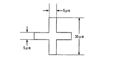
- FIG. 8 shows the shape of the alignment mark 720 formed on the semiconductor substrate 700.
- a GaN buffer layer 750, a GaN crystal 752, and an Al 0.2 Ga 0.8 N crystal 754 were formed in an opening formed in the inhibition layer 730 provided in the silicon substrate 710.
- an AlN buffer layer 760 having a thickness of 100 nm was formed on the main surface of the Si substrate with a plane orientation (111) off angle of 0 ° in a reactor having an internal temperature of 900 ° C.
- the obtained substrate was taken out from the reaction furnace.
- a photosensitive resin was applied on the AlN buffer layer 760.
- a cruciform opening exposing the AlN buffer layer 760 was formed by photolithography. As shown in FIG. 8, the opening has a shape in which two rectangles having a long side of 30 ⁇ m and a short side of 5 ⁇ m are overlapped so as to be orthogonal to each other at the center of each rectangle.
- the obtained substrate is transferred to a reactive ion etching apparatus chamber, and the alignment mark 720 is formed by dry etching the AlN buffer layer 760 exposed at the opening with SF6 gas plasma until the depth reaches 5 ⁇ m of the Si substrate. Formed. Next, the photosensitive resin adhering to other than the openings was removed with acetone.
- silicon oxide to be the inhibition layer 730 was deposited on the entire surface of the substrate with a thickness of 50 nm by the CVD method.
- An inhibition layer 732 was also formed on the alignment mark 720.
- Silane and oxygen were used as source gases.
- the substrate temperature was 600 ° C.
- a photosensitive resin pattern having a square opening with a side of 20 ⁇ m was formed on the inhibition layer 730 by a stepper exposure method. At this time, the alignment mark 720 formed earlier was positioned and exposed. The substrate was immersed in a 5% aqueous HF solution, and the silicon oxide exposed at the photosensitive resin opening was removed by etching to expose the AlN buffer layer 760.
- a GaN buffer layer 750 (thickness: 100 nm) is formed on the AlN buffer layer 760 exposed in the opening formed in the inhibition layer 730 by MOCVD with a growth temperature of 900 ° C. and a growth furnace pressure. Growing at 30 KPa.
- a GaN crystal 752 (thickness 2000 nm), which is a functional crystal, and then an Al 0.2 Ga 0.8 N crystal 754 (thickness 30 nm) were epitaxially grown by MOCVD at a growth temperature of 1060 ° C. and a growth furnace pressure of 12 MPa. Trimethylaluminum, trimethylgallium, and ammonia were used as the source gas.
- the obtained substrate was taken out of the MOCVD reactor and placed in a stepper exposure apparatus.
- a photosensitive resin opening having the shape of an ohmic electrode was formed on the substrate obtained by the stepper exposure method.
- Ti was deposited to a thickness of 150 nm and then Al was deposited to a thickness of 1500 nm, and a Ti / Al metal laminated structure having an electrode shape was formed by a lift-off method.
- an ohmic electrode was formed by annealing the substrate at 800 ° C. for 30 seconds.
- a photosensitive resin opening having the shape of the gate electrode was formed by a stepper exposure method.
- Ni was deposited to a thickness of 100 nm and then Au was deposited to a thickness of 2000 nm, and a Ni / Au metal laminated structure having an electrode shape was formed by a lift-off method. In this way, a gate electrode was formed.
- a semiconductor substrate having the alignment mark 720 on the Si substrate and the relative positions of the alignment mark 720, the semiconductor crystal, and the functional member being accurately defined can be manufactured. Since it is not necessary to newly form the alignment mark 720 used for forming the functional member after crystal growth of the semiconductor crystal, productivity can be improved.
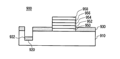
- FIG. 9 is a cross-sectional view of the manufactured semiconductor substrate 900.
- a GaAs buffer layer 950 In the semiconductor substrate 900, a GaAs buffer layer 950, an Al 0.2 Ga 0.8 As crystal 952, an In 0.15 Ga 0.85 As crystal 954, and an Al 0.2 Ga 0.8 As are disposed in an opening formed in the inhibition layer 930 provided on the GaAs substrate 910. Crystal 956 and n-GaAs crystal 958 were formed.
- a photosensitive resin was applied to the main surface of the GaAs substrate 910 having a plane orientation (001) off angle of 2 °.
- a cruciform opening through which the GaAs substrate 910 is exposed was formed by photolithography.
- the obtained substrate was transferred to a reactive ion etching apparatus chamber, and an alignment mark 920 was formed by dry etching the GaAs substrate 910 exposed to the opening with SF6 gas plasma until the depth reached 5 ⁇ m. Subsequently, the photosensitive resin was dissolved away with acetone.
- the silicon oxide as the inhibition layer 930 was deposited to a thickness of 50 nm on the entire surface of the substrate including the alignment mark 920 by CVD.
- An inhibition layer 932 was formed on the alignment mark 920.
- Silane and oxygen were used as source gases.
- the substrate temperature was 600 °.
- a photosensitive resin pattern having a square opening with a side of 20 ⁇ m was formed on silicon oxide by a stepper exposure method.
- the alignment mark 920 formed earlier was positioned and exposed.
- the substrate was immersed in a 5% aqueous HF solution, and silicon oxide exposed at the photosensitive resin opening was removed by etching to expose the GaAs substrate 910. Thereafter, the photosensitive resin is removed, and a GaAs buffer layer 950 (thickness: 100 nm) is formed on the GaAs substrate 910 exposed in the silicon oxide opening by MOCVD under a growth temperature of 600 ° C. and a growth furnace pressure of 10 KPa. Grown up.
- Al 0.2 Ga 0.8 As crystal 952 (thickness 2000 nm) which is a functional crystal
- In 0.15 Ga 0.85 As crystal 954 (thickness 20 nm)
- Al 0.2 Ga 0.8 As crystal 956 (thickness 200 nm)
- An n-GaAs crystal 958 (thickness 20 nm) was epitaxially grown at a growth temperature of 600 ° C. and a growth furnace pressure of 10 KPa.
- As the source gas trimethylaluminum, trimethylgallium, trimethylindium, and arsine were used.
- Silane was used as an n-type doping material.
- the alignment mark 920 is covered with the silicon oxide inhibition layer 932, the semiconductor crystal did not grow on the alignment mark 920. Therefore, the alignment mark 920 is not deformed by the crystal adhering to the alignment mark 920. As a result, a functional member can be formed with high alignment accuracy using the alignment mark 920 in the process of forming the functional member such as an electrode described below by photolithography.
- the obtained substrate was taken out of the MOCVD reactor and installed in a stepper exposure apparatus. While aligning the alignment mark 920, a photosensitive resin having an opening at a position corresponding to the position where the electrode is formed was formed by a stepper exposure method. Next, the silicon oxide HF aqueous solution in the opening was melted away. Subsequently, the photosensitive resin was dissolved away with acetone.
- a photosensitive resin having an opening having a shape corresponding to the ohmic electrode shape was formed by a stepper exposure method while performing alignment with the alignment mark 920 as a reference.
- Ti was deposited to a thickness of 150 nm and then Al was deposited to a thickness of 1500 nm, and a Ti / Al metal laminated structure having an electrode shape was formed by a lift-off method.
- the substrate was annealed at 800 ° C. for 30 seconds to form an ohmic electrode.
- a photosensitive resin opening having the shape of the gate electrode was formed by a stepper exposure method while performing alignment with the formed alignment mark 920 as a reference.
- Ni was deposited to a thickness of 100 nm and then Au was deposited to a thickness of 2000 nm, and a Ni / Au metal laminated structure having an electrode shape was formed by a lift-off method. In this way, a gate electrode was formed.
- a GaAs field effect transistor was formed as described above.
- a semiconductor substrate having the alignment mark 920 on the GaAs substrate 910 and the relative positions of the alignment mark 920 and the functional member such as the semiconductor crystal and the electrode can be accurately manufactured. Since it is not necessary to newly form an alignment mark used for forming the functional member after crystal growth of the semiconductor crystal, productivity can be improved.
Landscapes
- Physics & Mathematics (AREA)
- General Physics & Mathematics (AREA)
- Exposure And Positioning Against Photoresist Photosensitive Materials (AREA)
- Recrystallisation Techniques (AREA)
- Crystals, And After-Treatments Of Crystals (AREA)
- Exposure Of Semiconductors, Excluding Electron Or Ion Beam Exposure (AREA)
Abstract
Description
非特許文献1 S. Haffouz, et. al., Journal of crystal growth, 311(2009)2087-2090
特許文献1 特開平10-64781号公報
図7は、製造した半導体基板700の断面図である。図8は、半導体基板700に形成したアライメントマーク720の形状を示す。半導体基板700においては、シリコン基板710に設けられた阻害層730に形成された開口内に、GaNバッファ層750、GaN結晶752及びAl0.2Ga0.8N結晶754を形成した。
図9は、製造した半導体基板900の断面図である。半導体基板900においては、GaAs基板910に設けられた阻害層930に形成された開口内に、GaAsバッファ層950、Al0.2Ga0.8As結晶952、In0.15Ga0.85As結晶954、Al0.2Ga0.8As結晶956、n-GaAs結晶958を形成した。
Claims (18)
- ベース基板にアライメントマークを形成する段階と、
前記アライメントマークを形成する段階の後に、前記ベース基板上の前記アライメントマークを含む領域に、結晶成長を阻害する阻害層を形成する段階と、
前記アライメントマークの位置を基準とする開口を形成すべき位置を示す情報に基づいて、前記阻害層における前記アライメントマークが設けられていない領域に、前記ベース基板を露出する前記開口を形成する段階と、
前記開口内に半導体結晶を成長させる段階と
を備える半導体基板の製造方法。 - 前記アライメントマークの位置を基準として、前記半導体結晶上に電極及び金属配線のうちの少なくとも1つを形成する段階をさらに備える請求項1に記載の半導体基板の製造方法。
- 前記開口を形成する段階においては、前記アライメントマークが設けられていない領域に、複数の前記開口を形成する請求項1に記載の半導体基板の製造方法。
- 前記開口を形成する段階においては、前記アライメントマークの位置を基準とする前記複数の開口を形成すべき位置を示す情報に基づいて、前記複数の開口を形成する請求項3に記載の半導体基板の製造方法。
- 前記半導体結晶を成長させる段階においては、前記複数の開口のそれぞれに前記半導体結晶を成長させる請求項3に記載の半導体基板の製造方法。
- 前記アライメントマークの位置を基準として、前記複数の開口内のそれぞれの前記半導体結晶の上方に、電極及び金属配線のうちの少なくとも1つを含む機能部材を形成する機能部材形成段階をさらに備える請求項5に記載の半導体基板の製造方法。
- 前記機能部材形成段階においては、前記アライメントマークの位置を基準とするリソグラフィーにより、前記機能部材を形成する請求項6に記載の半導体基板の製造方法。
- 前記ベース基板が、表面がシリコン結晶である基板、表面がゲルマニウム結晶である基板又は3-5族化合物半導体基板である請求項1に記載の半導体基板の製造方法。
- 前記半導体結晶を成長させる段階において、3-5族化合物半導体結晶又は2-6族化合物半導体結晶を成長させる請求項1に記載の半導体基板の製造方法。
- 前記半導体結晶を成長させる段階は、
Cx1Siy1Gez1Sn1-x1-y1-z1(0≦x1<1、0≦y1≦1、0≦z1≦1、かつ0<x1+y1+z1≦1)の組成を有する第1の半導体結晶を成長させる段階と、
前記第1の半導体結晶上に第2の半導体結晶を成長させる段階と
を有する請求項1に記載の半導体基板の製造方法。 - 前記阻害層が、酸化シリコン、窒化シリコン、酸窒化シリコン又は酸化アルミニウムのいずれかを有する請求項1に記載の半導体基板の製造方法。
- 前記アライメントマークを形成する段階においては、前記ベース基板をエッチングすることにより前記アライメントマークを前記ベース基板に形成する請求項1に記載の半導体基板の製造方法。
- 前記アライメントマークを形成する段階においては、タンタル、ニオブ、ニッケル、タングステン及びチタンからなる群から選ばれる少なくとも1種の金属を前記ベース基板に形成することにより前記アライメントマークを前記ベース基板に形成する請求項1に記載の半導体基板の製造方法。
- アライメントマークが形成されたベース基板と、
前記ベース基板上の前記アライメントマークが形成された領域以外の領域に設けられた、前記ベース基板を露出する開口を有し、かつ、結晶成長を阻害する第1阻害層と、
前記アライメントマーク上に設けられ、かつ、結晶成長を阻害する第2阻害層と、
前記開口内で結晶成長した半導体結晶と
を備える半導体基板。 - 前記第1阻害層は、複数の前記開口を有し、
前記半導体基板は、前記複数の開口のそれぞれにおいて結晶成長した前記半導体結晶を備える請求項14に記載の半導体基板。 - 前記アライメントマークの位置における前記ベース基板の厚みと、前記アライメントマークの位置以外の前記ベース基板の領域における前記ベース基板の厚みとが異なり、
前記ベース基板の前記第1阻害層と接する面と反対の面である裏面から前記第1阻害層の前記ベース基板に近い面と反対の面までの距離は、前記裏面から前記第2阻害層の前記ベース基板に近い面と反対の面までの距離と異なる請求項14に記載の半導体基板。 - 前記アライメントマークの位置における前記ベース基板の厚みは、前記アライメントマークの位置以外の前記ベース基板の領域における前記ベース基板の厚みよりも小さく、
前記ベース基板の前記第1阻害層と接する面と反対の面である裏面から前記第1阻害層の前記ベース基板に近い面と反対の面までの距離は、前記裏面から前記第2阻害層の前記ベース基板に近い面と反対の面までの距離よりも大きい請求項16に記載の半導体基板。 - 前記アライメントマークの位置における前記ベース基板の厚みは、前記アライメントマークの位置以外の前記ベース基板の領域における前記ベース基板の厚みよりも大きく、
前記ベース基板の前記第1阻害層と接する面と反対の面である裏面から前記第1阻害層の前記ベース基板に近い面と反対の面までの距離は、前記裏面から前記第2阻害層の前記ベース基板に近い面と反対の面までの距離よりも小さい請求項16に記載の半導体基板。
Priority Applications (2)
| Application Number | Priority Date | Filing Date | Title |
|---|---|---|---|
| CN2010800502737A CN102598215A (zh) | 2009-11-26 | 2010-11-25 | 半导体基板及半导体基板的制造方法 |
| US13/479,834 US20120292789A1 (en) | 2009-11-26 | 2012-05-24 | Semiconductor wafer and method of producing the same |
Applications Claiming Priority (2)
| Application Number | Priority Date | Filing Date | Title |
|---|---|---|---|
| JP2009-268523 | 2009-11-26 | ||
| JP2009268523 | 2009-11-26 |
Related Child Applications (1)
| Application Number | Title | Priority Date | Filing Date |
|---|---|---|---|
| US13/479,834 Continuation-In-Part US20120292789A1 (en) | 2009-11-26 | 2012-05-24 | Semiconductor wafer and method of producing the same |
Publications (1)
| Publication Number | Publication Date |
|---|---|
| WO2011064997A1 true WO2011064997A1 (ja) | 2011-06-03 |
Family
ID=44066103
Family Applications (1)
| Application Number | Title | Priority Date | Filing Date |
|---|---|---|---|
| PCT/JP2010/006871 Ceased WO2011064997A1 (ja) | 2009-11-26 | 2010-11-25 | 半導体基板及び半導体基板の製造方法 |
Country Status (6)
| Country | Link |
|---|---|
| US (1) | US20120292789A1 (ja) |
| JP (1) | JP2011135060A (ja) |
| KR (1) | KR20120098666A (ja) |
| CN (1) | CN102598215A (ja) |
| TW (1) | TW201131733A (ja) |
| WO (1) | WO2011064997A1 (ja) |
Cited By (9)
| Publication number | Priority date | Publication date | Assignee | Title |
|---|---|---|---|---|
| JP2017533574A (ja) * | 2014-09-18 | 2017-11-09 | インテル・コーポレーション | シリコンcmos互換性半導体装置における欠陥伝播制御のための傾斜側壁カット面を有するウルツ鉱ヘテロエピタキシャル構造物 |
| US10211327B2 (en) | 2015-05-19 | 2019-02-19 | Intel Corporation | Semiconductor devices with raised doped crystalline structures |
| US10388777B2 (en) | 2015-06-26 | 2019-08-20 | Intel Corporation | Heteroepitaxial structures with high temperature stable substrate interface material |
| US10573647B2 (en) | 2014-11-18 | 2020-02-25 | Intel Corporation | CMOS circuits using n-channel and p-channel gallium nitride transistors |
| US10658471B2 (en) | 2015-12-24 | 2020-05-19 | Intel Corporation | Transition metal dichalcogenides (TMDCS) over III-nitride heteroepitaxial layers |
| US10756183B2 (en) | 2014-12-18 | 2020-08-25 | Intel Corporation | N-channel gallium nitride transistors |
| US11177376B2 (en) | 2014-09-25 | 2021-11-16 | Intel Corporation | III-N epitaxial device structures on free standing silicon mesas |
| US11233053B2 (en) | 2017-09-29 | 2022-01-25 | Intel Corporation | Group III-nitride (III-N) devices with reduced contact resistance and their methods of fabrication |
| US12125888B2 (en) | 2017-09-29 | 2024-10-22 | Intel Corporation | Group III-nitride (III-N) devices with reduced contact resistance and their methods of fabrication |
Families Citing this family (6)
| Publication number | Priority date | Publication date | Assignee | Title |
|---|---|---|---|---|
| JP2015032611A (ja) * | 2013-07-31 | 2015-02-16 | 住友電気工業株式会社 | 炭化珪素半導体装置の製造方法 |
| JP6257291B2 (ja) * | 2013-12-04 | 2018-01-10 | 株式会社ディスコ | パッケージ基板の加工方法 |
| JP2019020718A (ja) * | 2017-07-20 | 2019-02-07 | 住友化学株式会社 | 光学シート |
| JP2020141105A (ja) * | 2019-03-01 | 2020-09-03 | トヨタ自動車株式会社 | 半導体装置の製造方法 |
| US20250218972A1 (en) * | 2022-03-28 | 2025-07-03 | Sumitomo Electric Industries, Ltd. | Semiconductor substrate and semiconductor epitaxial substrate |
| JP7831879B2 (ja) * | 2022-09-01 | 2026-03-17 | 株式会社ジャパンディスプレイ | 半導体デバイス及びその製造方法 |
Citations (5)
| Publication number | Priority date | Publication date | Assignee | Title |
|---|---|---|---|---|
| JPH0484418A (ja) * | 1990-07-27 | 1992-03-17 | Nec Corp | 異種基板上への3―v族化合物半導体のヘテロエピタキシャル成長法 |
| JPH05343319A (ja) * | 1992-06-09 | 1993-12-24 | Sumitomo Electric Ind Ltd | 半導体装置の製造方法 |
| JPH1064781A (ja) * | 1996-08-14 | 1998-03-06 | Toshiba Corp | 位置検出マーク作成方法 |
| JP2001093834A (ja) * | 1999-09-20 | 2001-04-06 | Sanyo Electric Co Ltd | 半導体素子および半導体ウエハならびにその製造方法 |
| JP2002033458A (ja) * | 2000-07-19 | 2002-01-31 | Nikon Corp | 半導体装置及びその製造方法 |
Family Cites Families (6)
| Publication number | Priority date | Publication date | Assignee | Title |
|---|---|---|---|---|
| JPH10209010A (ja) * | 1997-01-21 | 1998-08-07 | Nikon Corp | 荷電ビーム露光方法,荷電ビーム露光装置およびパレット |
| JPH11224935A (ja) * | 1997-12-02 | 1999-08-17 | Mitsubishi Electric Corp | 半導体集積回路の基板及び半導体集積回路の製造方法 |
| KR100496139B1 (ko) * | 2002-12-30 | 2005-06-16 | 엘지.필립스 엘시디 주식회사 | 광학용 마스크, 이를 이용한 비정질 실리콘막의 결정화방법 및 어레이 기판의 제조 방법 |
| KR100539623B1 (ko) * | 2003-06-25 | 2005-12-28 | 엘지.필립스 엘시디 주식회사 | 버텀 게이트형 폴리 실리콘 박막트랜지스터 소자의 제조방법 |
| KR100573225B1 (ko) * | 2003-09-24 | 2006-04-24 | 엘지.필립스 엘시디 주식회사 | 비정질 실리콘층의 결정화 방법 |
| JP4029885B2 (ja) * | 2005-03-29 | 2008-01-09 | セイコーエプソン株式会社 | 半導体装置の製造方法 |
-
2010
- 2010-11-25 CN CN2010800502737A patent/CN102598215A/zh active Pending
- 2010-11-25 KR KR1020127011354A patent/KR20120098666A/ko not_active Withdrawn
- 2010-11-25 WO PCT/JP2010/006871 patent/WO2011064997A1/ja not_active Ceased
- 2010-11-25 JP JP2010262035A patent/JP2011135060A/ja active Pending
- 2010-11-26 TW TW099140961A patent/TW201131733A/zh unknown
-
2012
- 2012-05-24 US US13/479,834 patent/US20120292789A1/en not_active Abandoned
Patent Citations (5)
| Publication number | Priority date | Publication date | Assignee | Title |
|---|---|---|---|---|
| JPH0484418A (ja) * | 1990-07-27 | 1992-03-17 | Nec Corp | 異種基板上への3―v族化合物半導体のヘテロエピタキシャル成長法 |
| JPH05343319A (ja) * | 1992-06-09 | 1993-12-24 | Sumitomo Electric Ind Ltd | 半導体装置の製造方法 |
| JPH1064781A (ja) * | 1996-08-14 | 1998-03-06 | Toshiba Corp | 位置検出マーク作成方法 |
| JP2001093834A (ja) * | 1999-09-20 | 2001-04-06 | Sanyo Electric Co Ltd | 半導体素子および半導体ウエハならびにその製造方法 |
| JP2002033458A (ja) * | 2000-07-19 | 2002-01-31 | Nikon Corp | 半導体装置及びその製造方法 |
Cited By (13)
| Publication number | Priority date | Publication date | Assignee | Title |
|---|---|---|---|---|
| JP2017533574A (ja) * | 2014-09-18 | 2017-11-09 | インテル・コーポレーション | シリコンcmos互換性半導体装置における欠陥伝播制御のための傾斜側壁カット面を有するウルツ鉱ヘテロエピタキシャル構造物 |
| US10325774B2 (en) | 2014-09-18 | 2019-06-18 | Intel Corporation | Wurtzite heteroepitaxial structures with inclined sidewall facets for defect propagation control in silicon CMOS-compatible semiconductor devices |
| US10930500B2 (en) | 2014-09-18 | 2021-02-23 | Intel Corporation | Wurtzite heteroepitaxial structures with inclined sidewall facets for defect propagation control in silicon CMOS-compatible semiconductor devices |
| US11177376B2 (en) | 2014-09-25 | 2021-11-16 | Intel Corporation | III-N epitaxial device structures on free standing silicon mesas |
| US10573647B2 (en) | 2014-11-18 | 2020-02-25 | Intel Corporation | CMOS circuits using n-channel and p-channel gallium nitride transistors |
| US10756183B2 (en) | 2014-12-18 | 2020-08-25 | Intel Corporation | N-channel gallium nitride transistors |
| US10665708B2 (en) | 2015-05-19 | 2020-05-26 | Intel Corporation | Semiconductor devices with raised doped crystalline structures |
| US10211327B2 (en) | 2015-05-19 | 2019-02-19 | Intel Corporation | Semiconductor devices with raised doped crystalline structures |
| US10388777B2 (en) | 2015-06-26 | 2019-08-20 | Intel Corporation | Heteroepitaxial structures with high temperature stable substrate interface material |
| US10658471B2 (en) | 2015-12-24 | 2020-05-19 | Intel Corporation | Transition metal dichalcogenides (TMDCS) over III-nitride heteroepitaxial layers |
| US11233053B2 (en) | 2017-09-29 | 2022-01-25 | Intel Corporation | Group III-nitride (III-N) devices with reduced contact resistance and their methods of fabrication |
| US11728346B2 (en) | 2017-09-29 | 2023-08-15 | Intel Corporation | Group III-nitride (III-N) devices with reduced contact resistance and their methods of fabrication |
| US12125888B2 (en) | 2017-09-29 | 2024-10-22 | Intel Corporation | Group III-nitride (III-N) devices with reduced contact resistance and their methods of fabrication |
Also Published As
| Publication number | Publication date |
|---|---|
| TW201131733A (en) | 2011-09-16 |
| KR20120098666A (ko) | 2012-09-05 |
| US20120292789A1 (en) | 2012-11-22 |
| JP2011135060A (ja) | 2011-07-07 |
| CN102598215A (zh) | 2012-07-18 |
Similar Documents
| Publication | Publication Date | Title |
|---|---|---|
| WO2011064997A1 (ja) | 半導体基板及び半導体基板の製造方法 | |
| CN101207174B (zh) | 氮化物半导体衬底及其制造方法 | |
| US8058705B2 (en) | Composite material substrate | |
| US8652949B2 (en) | Method of manufacturing semiconductor wafer | |
| JP5192785B2 (ja) | 窒化物半導体装置の製造方法 | |
| KR20200066146A (ko) | 다이아몬드 기판 제조 방법 | |
| US10600645B2 (en) | Manufacturing method of gallium nitride substrate | |
| US7915747B2 (en) | Substrate for forming semiconductor layer including alignment marks | |
| US9583340B2 (en) | Semipolar nitride semiconductor structure and method of manufacturing the same | |
| US12243739B2 (en) | Semiconductor wafer and method for manufacturing same | |
| JP7308944B2 (ja) | 半導体素子の製造方法 | |
| US20180174822A1 (en) | Method of forming nitride semiconductor substrate and method of fabricating semiconductor device | |
| CN103456659A (zh) | 一种用于半导体器件制备的光刻对准标记制作方法 | |
| US9536955B2 (en) | Nitride semiconductor substrate | |
| US20160233293A1 (en) | A semiconductor wafer and a method for producing the semiconductor wafer | |
| US20240079412A1 (en) | Nitride semiconductor substrate and manufacturing method therefor | |
| CN118435320B (zh) | 半导体基板的制造方法、及其制造装置 | |
| KR101967716B1 (ko) | 질화갈륨 웨이퍼의 제조방법 | |
| WO2021066042A1 (ja) | 半導体素子の製造方法 | |
| CN108598238B (zh) | 一种形貌可控的GaN纳米线阵列的制备方法 | |
| JP5667360B2 (ja) | 半導体基板、電子デバイスおよび半導体基板の製造方法 | |
| CN100440429C (zh) | 半导体外延晶片及其制造方法 | |
| CN116825619A (zh) | 一种基于MOCVD的垂直GaN器件的掩膜钝化层生长方法 | |
| JPH04130717A (ja) | 結晶の形成方法 | |
| JPH0982640A (ja) | 化合物半導体基板とその製造方法 |
Legal Events
| Date | Code | Title | Description |
|---|---|---|---|
| WWE | Wipo information: entry into national phase |
Ref document number: 201080050273.7 Country of ref document: CN |
|
| 121 | Ep: the epo has been informed by wipo that ep was designated in this application |
Ref document number: 10832846 Country of ref document: EP Kind code of ref document: A1 |
|
| ENP | Entry into the national phase |
Ref document number: 20127011354 Country of ref document: KR Kind code of ref document: A |
|
| NENP | Non-entry into the national phase |
Ref country code: DE |
|
| 122 | Ep: pct application non-entry in european phase |
Ref document number: 10832846 Country of ref document: EP Kind code of ref document: A1 |