WO2011058838A1 - 受信装置 - Google Patents
受信装置 Download PDFInfo
- Publication number
- WO2011058838A1 WO2011058838A1 PCT/JP2010/067754 JP2010067754W WO2011058838A1 WO 2011058838 A1 WO2011058838 A1 WO 2011058838A1 JP 2010067754 W JP2010067754 W JP 2010067754W WO 2011058838 A1 WO2011058838 A1 WO 2011058838A1
- Authority
- WO
- WIPO (PCT)
- Prior art keywords
- display
- phase
- circuit
- signal
- imaging
- Prior art date
Links
Images


Classifications
-
- H—ELECTRICITY
- H04—ELECTRIC COMMUNICATION TECHNIQUE
- H04N—PICTORIAL COMMUNICATION, e.g. TELEVISION
- H04N21/00—Selective content distribution, e.g. interactive television or video on demand [VOD]
- H04N21/40—Client devices specifically adapted for the reception of or interaction with content, e.g. set-top-box [STB]; Operations thereof
- H04N21/43—Processing of content or additional data, e.g. demultiplexing additional data from a digital video stream; Elementary client operations, e.g. monitoring of home network or synchronising decoder's clock; Client middleware
- H04N21/443—OS processes, e.g. booting an STB, implementing a Java virtual machine in an STB or power management in an STB
-
- H—ELECTRICITY
- H04—ELECTRIC COMMUNICATION TECHNIQUE
- H04N—PICTORIAL COMMUNICATION, e.g. TELEVISION
- H04N21/00—Selective content distribution, e.g. interactive television or video on demand [VOD]
- H04N21/20—Servers specifically adapted for the distribution of content, e.g. VOD servers; Operations thereof
- H04N21/21—Server components or server architectures
- H04N21/218—Source of audio or video content, e.g. local disk arrays
- H04N21/2187—Live feed
-
- H—ELECTRICITY
- H04—ELECTRIC COMMUNICATION TECHNIQUE
- H04N—PICTORIAL COMMUNICATION, e.g. TELEVISION
- H04N21/00—Selective content distribution, e.g. interactive television or video on demand [VOD]
- H04N21/40—Client devices specifically adapted for the reception of or interaction with content, e.g. set-top-box [STB]; Operations thereof
- H04N21/43—Processing of content or additional data, e.g. demultiplexing additional data from a digital video stream; Elementary client operations, e.g. monitoring of home network or synchronising decoder's clock; Client middleware
- H04N21/4302—Content synchronisation processes, e.g. decoder synchronisation
- H04N21/4305—Synchronising client clock from received content stream, e.g. locking decoder clock with encoder clock, extraction of the PCR packets
-
- H—ELECTRICITY
- H04—ELECTRIC COMMUNICATION TECHNIQUE
- H04L—TRANSMISSION OF DIGITAL INFORMATION, e.g. TELEGRAPHIC COMMUNICATION
- H04L7/00—Arrangements for synchronising receiver with transmitter
- H04L7/02—Speed or phase control by the received code signals, the signals containing no special synchronisation information
- H04L7/033—Speed or phase control by the received code signals, the signals containing no special synchronisation information using the transitions of the received signal to control the phase of the synchronising-signal-generating means, e.g. using a phase-locked loop
Definitions
- the present invention relates to a receiving device that receives transmission data continuously transmitted from an imaging device at a predetermined cycle and performs display processing.
- transmission time information is created using a transmission clock, packetized with image data, and transmitted to a network.
- the received packet is decomposed and transmission time information and encoded data are extracted and stored in the fluctuation absorbing buffer, while the stored encoded data is read based on the transmission time information and the reference time, and a reference time Decrypt according to.
- the relative delay fluctuation time received by the received packet is further calculated based on the transmission time information and the reference time, and the reference time is calculated according to the smoothed relative delay fluctuation time for each received packet.
- the present invention has been made in view of the problems described above, and it is an object of the present invention to provide a receiving device capable of performing display processing in synchronization with the operation of an imaging device while suppressing an increase in the amount of transmission data. Do.
- the present invention was made to solve the above-mentioned problems.
- the receiving apparatus performs imaging processing at a predetermined cycle to create imaging data for each frame or field, packetizes the imaging data to create transmission data, and performs transmission processing for transmitting the transmission data.
- the processing unit may perform the phase adjustment processing so that display of the imaging data is started after a transmission possible period of the imaging data.
- an identification code may be added to the specific packet, and the measurement unit may measure the detection timing of the identification code as the reception timing of the specific packet.
- the specific packet may be a leading packet for each frame or field.
- the phase adjustment process includes a first process of instantaneously changing a phase of the display signal, and an adjustment of a frequency of a display clock used to generate the display signal.
- a second process of changing the phase of the display signal continuously may be included, and the processing unit may perform the second process only after performing the first process.
- the frequency of the display clock used to create the display signal is set to a predetermined value including adjustment values corresponding to predetermined upper and lower limit frequencies.
- a second process of setting the frequency of the display clock to an adjustment value such that the difference between the phase value of the display signal and the predetermined phase value is small Alternatively, the second process may be performed only after the first process has been performed.
- the phase adjustment process is a process of instantaneously changing the phase of the display signal, and the processing unit performs the blanking period which is a non-display period of the imaging data.
- the phase adjustment process may be performed.
- the measurement unit generates an estimated imaging timing signal in which an imaging timing corresponding to the predetermined cycle is estimated based on a result of the measurement, and the processing unit generates the estimated imaging timing signal.
- the phase adjustment process may be performed using
- the receiving device of the present invention further includes a storage unit that stores a plurality of algorithms related to the measurement, and the measurement unit is configured of the plurality of algorithms stored in the storage unit according to the result of the measurement.
- a predetermined algorithm may be selected, and the estimated imaging timing signal may be generated by the predetermined algorithm.
- the specific packet is extracted from the transmission data, and the phase adjustment processing of the display signal is performed using the result of measuring the reception timing of the specific packet multiple times.
- the display processing can be performed in synchronization with the operation of the imaging device while suppressing an increase in the amount of transmission data.
- FIG. 1 is a block diagram showing a configuration of an imaging phase detection circuit according to a first embodiment of the present invention.
- 5 is a timing chart showing the operation of the imaging phase detection circuit according to the first embodiment of the present invention.
- It is a reference drawing showing a histogram in a 1st embodiment of the present invention.
- It is a reference drawing showing a histogram in a 1st embodiment of the present invention.
- It is a reference drawing showing a histogram in a 1st embodiment of the present invention.
- a histogram in a 1st embodiment of the present invention is a reference drawing showing a histogram in a 1st embodiment of the present invention.
- imaging is performed at a predetermined cycle to create image data
- transmission data composed of a plurality of packets is created from the image data
- an imaging device that transmits transmission data by radio, and transmission data is received and displayed.
- the case where the embodiment of the present invention is applied to an imaging display system including a receiving device that generates a signal is described as an example. It is desirable that the imaging device and the receiving device are connected on a one-to-one basis or connected via a small scale network.
- FIG. 1 shows the configuration of the imaging display system according to the present embodiment.
- the imaging apparatus 1 includes an imaging optical system 2, an image sensor 3 (imaging element), an image processing circuit 4, a compression circuit 5, a packet generation circuit 6, an RF circuit 7, an antenna 8, a control circuit 9, and an imaging clock circuit 10. .
- the imaging optical system 2 forms an optical image of a subject on the image sensor 3.
- the image sensor 3 converts the formed optical image into imaging data and outputs the imaging data to the image processing circuit 4.
- the image sensor 3 in the present embodiment performs progressive scanning, and outputs imaging data in frame units at a predetermined cycle.
- the phase of the imaging data output from the image sensor 3 is referred to as an imaging phase.
- the image pickup data is subjected to image processing by the image processing circuit 4, converted into code data by the compression circuit 5, and added to the packet generation circuit 6.
- the packet generation circuit 6 combines code data for each predetermined data amount and adds well-known additional information including ID information which is an identification code for identifying a packet to generate a packet (transmission data).
- the operations of the image sensor 3, the image processing circuit 4, the compression circuit 5, the packet creation circuit 6, and the RF circuit 7 are controlled by the control circuit 9.
- the operation of the control circuit 9 is performed based on the imaging clock 11 from the imaging clock circuit 10. Therefore, the operation of the imaging device 1 is performed in synchronization with the imaging clock 11.
- the above-described method from the generation of imaging data by the image sensor 3 to the packetization of the imaging data is known, and therefore, further description will be omitted.
- the packet created by the packet creation circuit 6 is wirelessly transmitted by the RF circuit 7 via the antenna 8.
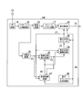
- the receiver 12 includes an antenna 13, an RF circuit 14, a packet separation circuit 15, an expansion circuit 16, a frame memory circuit 17, a display circuit 18, an ID detection circuit 20, an imaging phase detection circuit 22, a display phase adjustment circuit 24, and a display phase counter 26 includes a display clock frequency adjustment circuit 28, a display clock generation circuit 30, and a reception control circuit 32.
- the RF circuit 14 receives a radio signal via the antenna 13, demodulates the received radio signal, and outputs transmission data to the packet decomposition circuit 15.
- the packet decomposition circuit 15 decomposes the packet constituting the transmission data into code data and additional information, and outputs the code data to the expansion circuit 16 and the additional information to the ID detection circuit 20.
- the decompression circuit 16 decompresses the code data, converts it into image data, and outputs the image data to the frame memory circuit 17.
- Image data is stored in the frame memory circuit 17.
- the image data stored in the frame memory circuit 17 is appropriately read by the display circuit 18, converted (display processing) into the display signal 19 for display, and output.
- the phase of the display signal 19 is determined by the value of the display count signal 27 applied to the display circuit 18.
- the display count signal 27 is supplied from the display phase counter 26.
- the frequency of the display signal 19 is controlled by the display clock 31 applied to the display circuit 18.
- the display clock 31 is supplied from the display clock generation circuit 30.
- the ID detection circuit 20 detects ID information from the additional information of the head packet of the frame, creates an ID detection signal 21 indicating the detection timing of the ID, and outputs the signal to the imaging phase detection circuit 22 and the reception control circuit 32. .
- the imaging phase detection circuit 22 measures (measures) the reception timing of the head packet on the basis of the display count signal 27, thereby creating an imaging phase detection signal 23 (estimated imaging timing signal) indicating the imaging timing of the imaging device 1. Output.
- the imaging phase detection circuit 22 measures (measures) the ID detection signal 21 output from the ID detection circuit 20 a plurality of times with reference to the display count signal 27 to create a histogram, and processes the histogram. By doing this, the fluctuation of the packet transmission timing is removed and the imaging phase detection signal 23 is created. Details of the imaging phase detection circuit 22 will be described later with reference to FIGS. 3 to 7.
- the imaging phase detection signal 23 is output to the display phase adjustment circuit 24, the display clock frequency adjustment circuit 28, and the reception control circuit 32.
- the display phase adjustment circuit 24 controls the display phase counter 26 with the reset signal 25 to adjust the phase of the display signal 19.
- the display phase counter 26 generates a display count signal 27.
- the display clock frequency adjustment circuit 28 controls the display clock generation circuit 30 by the clock frequency control signal 29 to control the frequency of the display clock 31.
- the frequency control of the display clock 31 doubles as the phase adjustment of the display signal 19.
- the display clock generation circuit 30 generates a display clock 31.
- the reception control circuit 32 outputs a control signal 33 for controlling the operation of each part of the reception device 12.
- An ID detection signal 21, an imaging phase detection signal 23, a display count signal 27, and a display clock 31 are added to the reception control circuit 32, and a control signal 33 is generated from these signals. Details of the operation control of the receiver 12 by the reception control circuit 32 will be described later with reference to FIGS. 10A and 10B.
- an initial phase adjustment mode immediately after the start of the operation There are three operation modes of the reception device 12: an initial phase adjustment mode immediately after the start of the operation, an initial frequency adjustment mode performed subsequently to the initial phase adjustment mode, and a steady display mode performed after the initial frequency adjustment mode.
- the initial phase adjustment mode is a mode in which the display phase counter 26 is controlled to adjust the phase of the display signal 19 immediately after the reception device 12 starts reception.
- the display signal 19 is a signal for displaying black data.
- the initial frequency adjustment mode is a mode for performing processing of adjusting the frequency of the display clock 31 by the display clock frequency adjustment circuit 28 and synchronizing with the frequency of the imaging clock 11 after the end of the initial phase adjustment mode.
- the frequency of the display clock 31 is adjusted by the display clock frequency adjustment circuit 28, and the phase of the display signal 19 is adjusted to be a predetermined phase with respect to the imaging phase. Mode.
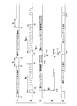
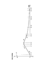
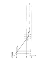
- FIG. 2 shows the relationship between the imaging phase of the imaging device 1 and the display phase of the receiving device 12 in the steady display mode.
- the first stage (uppermost stage) A in FIG. 2 shows the image sensor operation timing.
- the second stage B of FIG. 2 shows packet creation timing.
- the third stage C of FIG. 2 shows transmission timing.
- Between the third stage C and the fourth stage E in FIG. 2D an explanation of imaging / reception timing is shown.
- the fourth stage (bottom stage) E in FIG. 2 shows the display signal 19.
- the image sensor 3 outputs the imaging data of the Nth frame in the period from time t1 to t2, and puts a pause period (V blanking period) Q from time t2 to t3, and then from time t3 to t4.
- the operation of outputting the imaging data of the (N + 1) th frame in the period of is repeated.
- the period from time t1 to t3 is one frame period
- time t1 is the start point of the imaging phase
- time t3 is the end point of the imaging phase.
- the image sensor 3 operates at 30 frames per second
- the period from time t1 to t3 is 1/30 seconds (about 33.3 ms).
- the period from time t5 to t6 indicates the packet creation period G N of the Nth frame.
- the period from time t7 to t8 indicates the packet creation period G N + 1 of the (N + 1) th frame.
- the head of the packet in the packet creation time G N is the frame head packet h N.
- the top packet in the packet creation period G N + 1 is the frame top packet h N + 1 .
- the creation of a packet in the packet creation circuit 6 is started from the time (time t5) when the imaging data is compressed and data for one packet is prepared.
- the processing time in the compression circuit 5 changes depending on the design of the image pickup data (frequency component in the image pickup image), so jitter occurs in the period from time t1 to t5.
- Time t9 is timing when the imaging device 1 starts transmission of the leading packet of the Nth frame.
- Time t12 is timing when the receiving device 12 detects the ID of the leading packet.
- An arrow R1 indicates transmission of the ID of the head packet. Since the ID is added to the beginning of the packet, time t12 is immediately after time t9.
- the period from time t1 to t12 includes jitter accompanying communication (fluctuation of processing time of transmission processing, fluctuation of communication time due to retransmission processing due to deterioration of communication environment) in addition to jitter accompanying the compression processing. .
- a period from time t9 to t10 is a communication period of the packet of the Nth frame when there is no retransmission process.
- the period from time t9 to t11 is the longest communication period allowed when retransmission processing is performed.
- the communication including the retransmission process is not completed at time t11, the communication of the packet of the Nth frame is discontinued.
- An arrow R2 indicates that the communication of the packet is discontinued.
- the receiving device 12 measures (measures) the timing at time t12 (timing at which the ID of the head packet is detected) in each frame a plurality of times to create a histogram, and performs processing using the histogram. Then, the jitter component accompanying the communication, which is included in the time t12, is removed to estimate the operation timing of the imaging device 1, and the time of the time t11 is predicted.
- the reception device 12 detects the time t12 and adds a predetermined time corresponding to the interval (predetermined value) It10 to t12 of the time t12 to t11 to the time t12. The point in time is predicted.
- the reception device 12 adds the display processing time Td and the margin time (predetermined value) Tm to the time t11 to create the time t13. Then, the reception device 12 adjusts the phase of the display signal 19 so that the image of the Nth frame can be displayed from the time of time t13 (display signal top phase H).
- the display processing time Td described above is the time required for the processing for creating the display signal 19 (packet decomposition, decompression, frame memory writing / reading, display signal creation).
- the margin time Tm is a time obtained by adding various jitters and a measurement error.
- the receiver 12 re-executes the previous frame (N-1th frame) data without using the image data of the Nth frame in the display from time t13. use.
- the detection of the termination of the communication is performed by the reception control circuit 32 detecting from the ID detection signal 21 and using the detection result to control the display circuit 18 (control signal not shown).
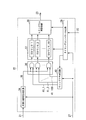
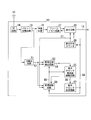
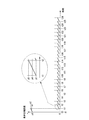
- FIG. 3 shows the configuration of the imaging phase detection circuit 22.
- FIG. 4 shows the operation of the imaging phase detection circuit 22.
- the imaging phase detection circuit 22 includes a head ID signal generation circuit 34, an AND gate block 36, an ID counter block 37, a histogram operation circuit 38, a timing control circuit 39, and a window generation circuit 40.
- the ID detection signal 21 and the display count signal 27 are input to the imaging phase detection circuit 22.
- the display count signal 27 is a signal indicating the number of counts in the display phase counter 26. As shown in FIG. 4, the display phase counter 26 counts 100 in one frame period F. Since one frame in the present embodiment is 1/30 seconds, one count period is 1/3000 seconds (about 0.333 ms).
- the display count signal 27 is added to the head ID signal generation circuit 34, the timing control circuit 39, and the window generation circuit 40.
- the ID detection signal 21 is applied to the head ID signal generation circuit 34.
- the start ID signal generation circuit 34 detects the start ID in the ID detection signal 21, creates a start ID signal 35 indicating the detection timing of the start ID, and outputs the start ID signal 35 to the AND gate block 36.
- the head ID signal 35 is a positive pulse signal generated in synchronization with the count of the display count signal 27.
- the waveform of the leading ID signal 35 is shown in FIG.
- the timing control circuit 39 creates a control signal for controlling the operation of each circuit in the imaging phase detection circuit 22 using the control signal 33 from the reception control circuit 32 and the display count signal 27.
- the window generation circuit 40 generates 100 window signals (window 41 _ 1 to window 41 _ 100) which become HI level for each count value of the display count signal 27 and outputs it to the AND gate block 36.
- the count value of the display count signal 27 will be described as the display count signal phase.
- the AND gate block 36 detects at which phase of the display count signal 27 the pulse of the first ID signal 35 is generated using the first ID signal 35 and the window signal (41_1 to 41_100), and corresponds to each phase.
- the count up signal is supplied to the counter (ID counter_1 to ID counter_100).
- the AND gate block 36 has a structure in which 100 2-input AND gates are combined.
- the first ID signal 35 is applied to one input of each AND gate, and the window signal is applied to the other input.
- the output of each AND gate is supplied to the ID counter _1 to the ID counter _ 100 in the ID counter block 37.
- the ID counter block 37 is a circuit composed of 100 ID counters _1 to 100.
- the ID counter block 37 creates a histogram of the phase of the leading ID signal 35 by counting the number of occurrences of the leading ID signal for each count value (phase) of the display count signal 27.
- the outputs of the ID counters _1 to ID counter _ 100 are supplied to the histogram calculation circuit 38.
- the histogram calculation circuit 38 performs calculation processing using the histogram data from the ID counter block 37 according to the operation mode of the receiving device 12 notified from the timing control circuit 39, and detects the imaging phase indicating the transmission timing of the leading ID. Create a signal 23.
- the contents of the arithmetic processing will be described later with reference to FIGS. 5 to 7.
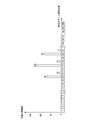
- the histogram in the present embodiment will be described. 5 to 7 show examples of histograms.
- the vertical axis indicates the cumulative number of start IDs (the values of the ID counter_1 to the ID counter 100).
- the horizontal axis indicates the display count signal phase (count value of the display count signal 27).
- the measurement period for creating the histogram is 10 seconds. Since the measurement period is 10 seconds and the imaging cycle is 30 frames / second, the total number of detections of the leading ID signal is "300".
- the phase of the leading ID changes due to the fluctuation of the compression processing time, the fluctuation of the communication processing time, and the fluctuation due to the frequency difference between the imaging clock frequency and the display clock frequency.
- the variation of the compression processing time is a variation that occurs because the content of the compression processing changes according to the frequency component included in the captured image.
- the fluctuation range is a known value determined by the performance of the compression circuit 5. Fluctuations in communication time include fluctuation due to retransmission processing caused by deterioration of the communication path and fluctuation in processing time inside the RF circuit 7. The interval at which the retransmission process is performed and the fluctuation range of the processing time inside the RF circuit 7 are known values determined by the RF circuit 7.
- the variation of the compression processing time and the variation of the processing time inside the RF circuit 7 are smaller than the variation due to the re-transmission processing described later and the variation due to the frequency difference between the imaging clock frequency and the display clock frequency.
- processing is performed in which the fluctuation ranges of both the fluctuations are added and included in the adjustment margin.
- the interval at which the retransmission process is performed is an interval of 1 ms.
- the reception timing of the packet is shifted by 3 counts in the display count signal phase. For example, when the head ID is at the position of the display count signal phase '20', when the head packet is retransmitted, the retransmitted head packet is detected at the position of the display count signal phase '23'.
- the influence of the frequency difference between the imaging clock frequency and the display clock frequency on the histogram will be described.
- the frequency difference between the imaging clock frequency and the display clock frequency is 60 ppm (60E-6)
- the timing of imaging and display shifts by 0.6 ms during the measurement period of 10 seconds.
- 0.6 ms corresponds to about 2 counts in the display count signal phase. Therefore, when the start ID is at the position of the display count signal phase '20' at the beginning of measurement, the start ID becomes the position of the display count signal phase '22' at the end of the measurement.
- the frequency of the display clock 31 is adjusted to substantially the same frequency as the frequency of the imaging clock 11. Therefore, there is no deviation of the display count signal phase due to the frequency difference between the imaging clock frequency and the display clock frequency.
- FIG. 5 and 6 are examples of histograms in the steady display mode.
- FIG. 5 shows a communication state in which the number of retransmission processes is small.
- FIG. 6 shows a communication state in which there are many retransmissions.
- the accumulated number of the leading ID is distributed between the display count signal phases '19' to '22', and particularly distributed to the phases '20' and '21'.
- the accumulated number of the leading ID is distributed in three count increments, that is, display count signal phases '20', '23', and '26' according to the occurrence of retransmission.
- the method of detecting the phase value output as the imaging phase detection signal 23 differs depending on the shape of the histogram. Specifically, the histogram calculation circuit 38 detects the frequency of occurrence of retransmission from the distribution state of the display count signal phase in which the cumulative number of the top ID in the histogram is larger than the reference number (in this description, “50”). The histogram operation circuit 38 outputs the display count signal phase of the smallest numerical value among the display count signal phases whose accumulated number exceeds the reference number when it is determined that the occurrence of retransmission is large as the imaging phase detection signal 23.
- the reference number in this description, “50”.
- the histogram operation circuit 38 outputs the display count signal phase with the largest cumulative number among the display count signal phases whose cumulative number exceeds the reference number as the imaging phase detection signal 23 Do.
- the determination is made on the basis of the distribution of display count signal phases whose accumulated number is equal to or greater than the reference number. Specifically, when the display count signal phase in which the cumulative number is equal to or larger than the reference number is continuous, the histogram calculation circuit 38 determines that the occurrence of retransmission is small. On the other hand, the histogram calculation circuit 38 determines that there are many occurrences of retransmission when the count is dispersed at about 3 counts.
- the value of the imaging phase detection signal 23 is determined to '20', which is the value of the display count signal phase having the largest cumulative number.
- the value of the imaging phase detection signal 23 is determined to be "20" which is the smallest numerical value among the display count signal phases whose accumulated number exceeds the reference number.
- the histogram calculation circuit 38 detects the frequency of occurrence of retransmission from the histogram indicating the measurement result of the reception timing of the leading ID, and selects an algorithm corresponding to the detected frequency from a plurality of algorithms. And the value of the imaging phase detection signal 23 is determined according to the algorithm. Information on a plurality of usable algorithms is stored in a memory (not shown).
- FIG. 7 is a histogram in the initial phase adjustment mode or the initial frequency adjustment mode, and is an example in the case where the frequency difference is large (approximately 60 ppm). Since the frequency adjustment is not performed in the initial phase adjustment mode and the initial frequency adjustment mode, as described above, for example, when the frequency difference is about 60 ppm, the timing of imaging and display during the measurement period of 10 seconds is the display count signal phase Will shift about 2 counts. Therefore, as shown in FIG. 7, the display count signal phase in which the cumulative number is equal to or more than the reference number is continuous, and the continuous width is determined according to the frequency difference.
- the histogram calculation circuit 38 corresponds to the above situation in the initial phase adjustment mode and the initial frequency adjustment mode, and therefore the median value (the smaller value if it can not be divided by '2') of the display count signal phase greater than the reference number.
- the value is output as the value of the imaging phase detection signal 23.
- the display count signal phases above the reference number are '21', '22', '23' and '24', the smaller '22' of the median '22' and '23' is The value is output as the value of the imaging phase detection signal 23.
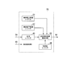
- FIG. 8 shows the configuration of the display phase adjustment circuit 24.
- the display phase adjustment circuit 24 controls the display phase counter 26 in the initial phase adjustment mode, and adjusts the phase of the display signal 19 so that the phase of the display signal 19 becomes a predetermined phase with respect to the imaging phase.
- the display phase adjustment circuit 24 has a reference value register 42, a subtraction circuit 43, and a reset timing generation circuit 45.
- a display count signal 27 from the display phase counter 26, an imaging phase detection signal 23 from the imaging phase detection circuit 22, and a control signal 33 from the reception control circuit 32 are added to the display phase adjustment circuit 24. Control of the display phase counter 26 by the display phase adjustment circuit 24 is performed only once immediately after the reception device 12 starts receiving the transmission signal from the imaging device 1.
- the reference register 42 prestores, as a reference value, an output value of the imaging phase detection signal 23 when the phase of the display signal 19 is adjusted to the optimal phase with respect to the imaging phase (hereinafter referred to as the optimal phase). ing.
- the subtraction circuit 43 subtracts the value of the imaging phase detection signal 23 from the value of the reference register 42.
- the subtraction output 44 from the subtraction circuit 43 is output to the reset timing generation circuit 45.
- the reset timing generation circuit 45 outputs the reset signal 25 to the display phase counter 26 only once to reset the display phase counter 26.
- the value stored in the reference register 42 is "20"
- the display phase adjustment circuit 24 delays the display phase by 40 counts by resetting the display phase counter 26 to "0" when the display count becomes "40". That is, when the value of the imaging phase detection signal 23 is "60", the subtraction output 44 is "40", and the reset timing generation circuit 45 displays the reset signal 25 when the display count signal 27 becomes “40". The value is outputted to the phase counter 26 and the value of the display phase counter 26 is made "0". By the above processing, the display signal 19 is adjusted to the optimum phase, and the initial phase adjustment mode is ended.
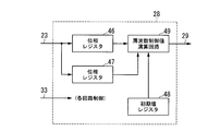
- the display clock frequency adjustment circuit 28 is a circuit that outputs a clock frequency control signal 29 that adjusts the clock frequency of the display clock 31.
- the display clock frequency adjustment circuit 28 includes a phase register 46, a phase register 47, an initial value register 48, and a frequency control value calculation circuit 49.
- An imaging phase detection signal 23 and a control signal 33 are added to the display clock frequency adjustment circuit 28.
- the imaging phase detection signal 23 is applied to the phase register 46 and the phase register 47, and values are held in each register in accordance with an instruction from the control signal 33.
- the values of the phase register 46 and the phase register 47 are output to the frequency control value calculation circuit 49.
- the value of the initial value register 48 is also added to the frequency control value calculation circuit 49.
- the frequency control value calculation circuit 49 generates the clock frequency control signal 29 from the values of the phase register 46, the phase register 47 and the initial value register 48.
- the frequency control value calculation circuit 49 In the initial phase adjustment mode, the frequency control value calculation circuit 49 generates the clock frequency control signal 29 using the value of the initial value register 48.
- the initial value register 48 stores the initial value (the center value of the frequency adjustment range) of the clock frequency of the display clock 31.
- the values of the imaging phase detection signal 23 measured at predetermined measurement intervals are stored in the phase register 46 and the phase register 47, and the frequency control value calculation circuit 49 outputs the phase register 46 and the phase register 47.
- the clock frequency control signal 29 is generated using the difference of values.
- the frequency control value calculation circuit 49 calculates the output value of the phase register 46 and the output value of the clock frequency control signal 29 at that time. A clock frequency control signal 29 is created.
- the operation in the initial frequency adjustment mode and the steady display mode are shown below.
- 10 seconds measurement (stores a value in the phase register 47)-50 seconds wait-10 seconds measurement (stores a value in the phase register 46)-A sequence of frequency adjustment is performed once.
- the period from the central time of the measurement period to the central time of the next measurement period is 60 seconds.
- the frequency control value calculation circuit 49 determines that the frequency difference is 55.6 ppm, and the output frequency of the display clock generation circuit 30 is 55.6 ppm The output value of the clock frequency control signal 29 is adjusted to be low.
- the sequence of 10 seconds measurement (stores a value in the phase register 46) -frequency adjustment-50 seconds wait is repeated.
- the frequency control value calculation circuit 49 causes the clock frequency to approach the value of the imaging phase detection signal 23 when the phase of the display signal 19 is the optimal phase with respect to the imaging phase of the imaging device 1
- the output value of the control signal 29 is adjusted.
- the frequency control value calculation circuit 49 obtains the amount of deviation from the optimum phase of the measurement result, and performs control so that the amount of deviation becomes 1/2 in the next measurement. For example, when the optimum phase is '20' and the measurement result is '28', the frequency control value calculation circuit 49 performs frequency adjustment so that the next measurement result is '24'. If there is 60 seconds before the next measurement, the frequency of the display clock 31 may be shifted by about 5.56 ppm to shift the value of the imaging phase detection signal 23 by one count. In the above case, since the measurement result is '28' and the target value for the next measurement is '24', the frequency control value calculation circuit 49 is made to be lower than the current frequency by 22.24 ppm which is four counts of the difference. The output value of the clock frequency control signal 29 is adjusted.
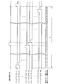
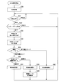
- FIG. 10A and 10B show the phase adjustment operation in the receiving device 12.
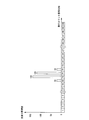
- FIG. 11 is an example of a schematic diagram showing a change in difference between an actual display phase and a preset optimum display phase (hereinafter referred to as a display phase error) immediately after the start of operation.
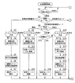
- the adjustment mode is the initial phase adjustment mode.
- the ID detection circuit 20 waits for detection of the top ID (S1), and the reception control circuit 32 checks the adjustment mode after detection of the top ID (S2). If the adjustment mode is the initial phase adjustment mode, the reception control circuit 32 checks whether a histogram is being generated (measured) (S3). When the measurement is completed, the imaging phase detection circuit 22 creates an imaging phase detection signal 23 according to the control signal 33 from the reception control circuit 32 (S4).
- the display phase adjustment circuit 24 After generation of the imaging phase detection signal 23, the display phase adjustment circuit 24 performs display phase adjustment according to the control signal 33 from the reception control circuit 32 (S5). Thereafter, the reception control circuit 32 sets the adjustment mode to the initial frequency adjustment mode (S6), sets the measurement mode to the measurement 1 (S7), and ends the initial phase adjustment mode.
- the above operation corresponds to the period of time t0 to t1 in FIG.
- p0 is a display phase error at the start of the initial phase adjustment mode
- p1 is a display phase error at the end of the initial phase adjustment mode.
- the difference between p0 and p1 is due to the frequency difference between the imaging clock and the display clock.
- the frequency control value calculation circuit 49 generates the clock frequency control signal 29 using the initial value of the clock frequency stored in the initial value register 48 between S2 and S3.
- the initial frequency adjustment mode After the detection of the head ID, it is determined that the adjustment mode is the initial frequency adjustment mode (S2). In the case of the initial frequency adjustment mode, the operation changes depending on the measurement mode. The period during which measurement 1 is performed is the first phase measurement period. The period during which waiting 1 is performed is waiting time. The period during which measurement 2 is performed is the second phase measurement period. The reception control circuit 32 checks the measurement mode (S8).
- the reception control circuit 32 checks whether a histogram is being generated (during measurement) (S9).
- the imaging phase detection circuit 22 creates an imaging phase detection signal 23 according to the control signal 33 from the reception control circuit 32 (S10).
- the value of the imaging phase detection signal 23 is stored in the phase register 47 (S11).
- the reception control circuit 32 sets the measurement mode to standby 1 (S12), and ends the first measurement.
- the reception control circuit 32 checks whether the standby is completed until 50 seconds elapse (S13). After waiting for 50 seconds, the reception control circuit 32 sets the measurement mode to measurement 2 (S14) and ends the processing of standby 1, and the processing shifts to the second phase measurement (measurement 2).
- the reception control circuit 32 checks whether a histogram is being generated (during measurement) (S15).
- the imaging phase detection circuit 22 creates the imaging phase detection signal 23 according to the control signal 33 from the reception control circuit 32 (S16).
- the value of the imaging phase detection signal 23 is stored in the phase register 46 (S17).
- the display clock frequency adjustment circuit 28 performs frequency adjustment 1 (S18).
- the details of the frequency adjustment 1 (S18) have been described in the description of the operation in the initial frequency adjustment mode of the frequency control value calculation circuit 49 using FIG. 9, so the description will be omitted here.
- the reception control circuit 32 sets the adjustment mode to the steady display mode (S19), sets the measurement mode to the measurement 3 (S20), and ends the initial frequency adjustment mode.
- the operation in the initial frequency adjustment mode corresponds to the period from time t1 to t4 in FIG.
- the period from time t1 to t2 is the first phase measurement period
- the period from time t2 to t3 is the waiting 1 period
- the period from time t3 to t4 is the second phase measurement period and frequency adjustment processing (S18) Implementation period of The increase in the display phase error in the period from time t1 to t4 is because frequency adjustment is not performed.
- the steady display mode In the steady display mode, after the detection of the head ID, it is determined that the adjustment mode is the steady display mode (S2). Thereafter, the reception control circuit 32 checks the measurement mode (S21).
- the steady display mode has two measurement modes, measurement 3 and standby 2. In measurement 3, the measurement of the display phase error and the adjustment of the frequency are performed, and in standby 2, the next measurement is awaited.
- the reception control circuit 32 checks whether a histogram is being generated (during measurement) (S22).
- the imaging phase detection circuit 22 creates the imaging phase detection signal 23 according to the control signal 33 from the reception control circuit 32 (S23).
- the value of the imaging phase detection signal 23 is stored in the phase register 46 (S24).
- the display clock frequency adjustment circuit 28 performs frequency adjustment 2 (S25).
- the details of the frequency adjustment 2 (S25) have been described in the description of the operation in the steady display mode of the frequency control value calculation circuit 49 using FIG. 9, so the description will be omitted here.
- the operation in the steady display mode corresponds to the period from time t4 to t13 in FIG.
- Clock 3 is performed so that measurement 3 is performed in the period from time t4 to time t5, and the measured display phase error (p4) is halved in the next measurement (time t6 to t7) (calculation interval is 60 seconds).
- the output value of the frequency control signal 29 is adjusted.
- the display phase error (p5) at the next measurement (time t6-t7) is 1/2 of p4.
- the reception timing of the specific packet is measured a plurality of times in the reception device 12, the imaging period is estimated using the measurement result, and the display signal 19 is displayed based on the estimated imaging period.
- the phase is adjusted. Therefore, the display processing can be performed in synchronization with the operation of the imaging device 1, and the delay time of the display image can be further reduced without causing the overflow and the underflow.
- phase adjustment is possible even in a system that performs retransmission processing.
- phase adjustment process of the present embodiment a phase reset process (S5) in which the phase of the display signal 19 is instantaneously changed by the display phase adjustment circuit 24 resetting the display phase counter 26, and the display clock frequency adjustment circuit 28.
- the value of the imaging phase detection signal 23 is determined according to the algorithm selected according to the frequency of occurrence of retransmission detected from the histogram by the histogram calculation circuit 38 to cope with the disturbance of the measurement result due to the occurrence of retransmission.
- An accurate imaging phase detection signal 23 can be generated.
- the output form of imaging data and the phase adjustment method are different.
- the present embodiment is an example in which the image sensor 3 performs the interlace scan. In the case of interlaced scanning, one frame consists of two fields, odd and even. Since the interlace scan is known, further description will be omitted.
- the phase adjustment of this embodiment is performed only by frequency adjustment of the display clock signal.
- FIG. 12 shows the configuration of a receiving device 50 according to this embodiment. 12, the circuits having the same functions as those of the receiver 12 shown in FIG. 1 are assigned the same reference numerals, and the circuit which is the main operation of this embodiment is the circuit of the receiver 12 shown in FIG. Different numbers are attached.
- the receiving device 50 includes an antenna 13, an RF circuit 14, a packet separation circuit 15, an expansion circuit 16, a frame memory circuit 17, a display circuit 18, a display phase counter 26, an ID detection circuit 51, an imaging phase detection circuit 53, and a display clock frequency adjustment.
- a circuit 55, a display clock generation circuit 57, and a reception control circuit 59 are included.
- the ID detection circuit 51 detects ID information from the additional information of the head packet of the field, creates an ID detection signal 52 indicating the detection timing of the ID, and outputs the signal to the imaging phase detection circuit 53 and the reception control circuit 59. .
- the imaging phase detection circuit 53 measures (measures) the reception timing of the head packet on the basis of the display count signal 27 to create and output an imaging phase detection signal 54 indicating the imaging timing of the imaging device 1.
- the display clock frequency adjustment circuit 55 generates a clock frequency control signal 56 based on the imaging phase detection signal 54, and controls the display clock generation circuit 57 by the clock frequency control signal 56 to control the frequency of the display clock 58.
- the display clock generation circuit 57 generates a display clock 58.
- the reception control circuit 59 outputs a control signal 60 for controlling the operation of each part of the reception device 50.
- the initial adjustment mode measures the display phase error which is the difference between the actual display phase and the optimal display phase, and limits the frequency of the display clock 58 to the upper limit frequency and the lower limit frequency until the display phase error falls within a predetermined allowable range. It is a mode to maintain in either.
- the frequency of the display clock 58 is used as a central value to shift to the steady display mode.
- the steady display mode is a mode in which the display phase error is continuously measured and the frequency of the display clock 58 is controlled so that the display phase error becomes zero.
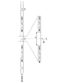
- FIG. 13 shows the relationship between the imaging phase of the imaging device 1 and the display phase of the receiving device 50 in the steady display mode in which the display phase is synchronized with the imaging phase.
- the first stage (uppermost stage) A in FIG. 13 shows the image sensor operation timing.
- the second stage B of FIG. 13 shows packet creation timing.
- the third stage C of FIG. 13 shows transmission timing.
- D illustrates the imaging / reception timing.
- the fourth stage (bottom stage) E in FIG. 13 shows a display signal.
- the image sensor 3 outputs the imaging data of the Nth frame odd field in the period from time t1 to t2, puts a pause period from time t2 to t3, and outputs the imaging data from time t3 to t4.
- the imaging data of N frame even field is output, and the imaging data of the (N + 1) th frame odd field is output in the period of time t5 to t6 with an idle period of time t4 to t5, and the imaging data of N + 1 frame odd field is output
- the operation of repeating the operation of outputting the imaging data of the (N + 1) -th frame even field during the period from time t7 to time t8 is repeated with a period.
- the period from time t1 to t5 is one frame period, and time t1 is the start point of the imaging phase, and time t5 is the end point of the imaging phase.
- the image sensor 3 operates at 30 frames per second, and one field (time t1-t3 and time t3-t5) period is 1/60 seconds (about 16.6 ms).
- a period of time t9 to t10 indicates a packet creation period G.
- the leading packet in the packet creation period G is a frame leading packet h.
- the packet creation in the packet creation circuit 6 is started from the time (time t9) when the imaging data is compressed and data for one packet is prepared.
- Time t17 is timing to start transmission of the leading packet of the Nth frame.
- An arrow R3 indicates the transmission of the ID of the packet at the beginning of the frame.
- Time t23 is timing when the receiving device 50 detects the ID of the leading packet. Since the ID is added to the beginning of the packet, it is detected immediately after time t17.
- the period from time t1 to t23 includes jitter accompanying communication (fluctuation of processing time of transmission processing, fluctuation of communication time due to retransmission processing due to deterioration of communication environment) in addition to jitter accompanying the compression processing. .
- the period from time t17 to t18 is a communication period of the packet of the Nth frame when there is no retransmission processing.
- the period from time t17 to t19 is the longest communication period allowed when retransmission processing is performed. When the communication including the retransmission process is not completed at time t19, the communication of the packet of the Nth frame odd field is discontinued.
- Communication of a packet of the Nth frame even field is performed in a period from time t20 to time t22.
- the head packet of the field is output at time t20 delayed by 1/60 seconds from time t17.
- An arrow R4 indicates transmission of the ID of the packet at the head of the field.
- the ID detection timing of the head packet of the even field is also used to generate the imaging phase detection signal 23. More specifically, the timing at which the correction for the phase equivalent to 1/60 seconds is performed to the ID detection timing of the head packet of the even field is referred to as the ID of the frame top packet (ID detection timing of the head packet of the odd field) It is used with the detection timing of to create a histogram.
- An arrow R5 indicates that the communication of the packet of the Nth frame even field is discontinued.
- FIG. 14 shows the configuration of the display clock frequency adjustment circuit 55.
- all the phases of the display signal 19 are adjusted by adjusting the frequency of the display clock 58.
- a display clock frequency adjustment circuit 55 controls the frequency of the display clock 58.
- the display clock frequency adjustment circuit 55 has a phase register 46, an initial value register 48, an upper frequency limit value register 61, a lower frequency range value register 62, and a frequency control value calculation circuit 63.
- the frequency upper limit value register 61, the frequency lower limit value register 62, and the initial value register 48 are used to adjust the phase of the display signal 19 in the initial adjustment mode.
- An upper limit value of a predetermined frequency range is stored in the frequency upper limit value register 61.
- the frequency lower limit value register 62 stores the lower limit value of the predetermined frequency range.
- the initial value register 48 stores the central value of the predetermined frequency adjustment range.
- the frequency control value calculation circuit 63 generates the clock frequency control signal 56 from the values of the phase register 46, the initial value register 48, the frequency upper limit register 61, and the frequency lower limit register 62.
- FIG. 15 shows the phase adjustment operation in the reception device 50.
- FIG. 16 is an example of a schematic diagram showing the change in the difference between the actual display phase and the optimum display phase (display phase error) immediately after the start of operation.
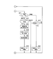
- the adjustment mode is the initial adjustment mode.
- an initial adjustment S30
- the reception control circuit 59 sets the adjustment mode to the initial adjustment mode
- the display clock frequency adjustment circuit 55 sets the display clock frequency to the central value using the value of the initial value register 48.
- the ID detection circuit 51 waits for detection of the leading ID (S31), and the reception control circuit 59 checks whether a histogram is being generated (measured) (S32).
- the imaging phase detection circuit 53 creates an imaging phase detection signal 54 in accordance with the control signal 60 from the reception control circuit 59 (S33).
- the value of the imaging phase detection signal 54 is stored in the phase register 46 of the display clock frequency adjustment circuit 55 (S34). The operation immediately after the start of the operation up to this point corresponds to the period of time t0 to t1 in FIG.
- the reception control circuit 59 checks the measurement mode (S35). If the measurement mode is the initial adjustment mode, the reception control circuit 59 determines whether the display phase error is within the allowable phase range (S36). If the display phase error is out of the allowable phase range, the display clock frequency adjustment circuit 55 performs frequency adjustment 1 (S37) in accordance with the control signal 60 from the reception control circuit 59.
- the frequency control value calculation circuit 63 of the display clock frequency adjustment circuit 55 sets the frequency upper limit value register 61 and the frequency lower limit value according to the display phase error corresponding to the value stored in the phase register 46.
- One of the registers 62 is selected.
- the clock frequency control signal 56 corresponding to the value stored in the selected register is created and output.
- the range of pK + to pK- in FIG. 16 is the allowable phase range.
- the frequency upper limit value register 61 is selected. If the display phase error is less than pK ⁇ , the frequency lower limit value register 62 is selected.
- the frequency control value calculation circuit 63 of the display clock frequency adjustment circuit 55 performs frequency adjustment 2 (S38) in accordance with the control signal 60 from the reception control circuit 59.
- the frequency control value calculation circuit 63 sets the value stored in the initial value register 48 instead of the frequency upper limit value register 61 or the frequency lower limit value register 62 as a control value.
- the reception control circuit 59 sets the adjustment mode to the steady display mode (S39).
- the frequency upper limit value register 61 The value of the clock frequency control signal 56 is created.
- the detected display phase error falls within the allowable phase range at the time shown by time t4 to t5.
- the adjustment mode is the initial adjustment mode. After time t5, the adjustment mode becomes the steady display mode.
- the steady display mode Unlike the first embodiment, in the steady display mode of the present embodiment, the measurement (frequency adjustment) processing is continuously performed without performing the standby processing.
- the processing from the waiting for detection of the head ID (S31) to the storage of the value in the phase register 46 (S34) is sequentially performed.
- the reception control circuit 59 checks the adjustment mode (S35). Since the adjustment mode is the steady display mode, the display clock frequency adjustment circuit 55 performs frequency adjustment 3 (S40) in accordance with the control signal 60 from the reception control circuit 59.
- the frequency control value calculation circuit 63 of the display clock frequency adjustment circuit 55 uses the current frequency control value and the detected display phase error to reduce the display phase error.
- the control signal 56 is adjusted.
- the details of the adjustment for reducing the display phase error are known as positioning control theory, and thus the description thereof is omitted.
- the reception timing of the specific packet is measured a plurality of times in the reception device 50, the imaging cycle is estimated using the measurement result, and the display clock 58 is calculated based on the estimated imaging cycle.
- the phase of the display signal 19 is adjusted by adjusting the frequency. Therefore, the display processing can be performed in synchronization with the operation of the imaging device 1, and the delay time of the display image can be further reduced without causing the overflow and the underflow. Further, since it is possible to adjust the phase of the display signal 19 only by adjusting the frequency of the display clock 58, it is possible to suppress an increase in hardware.
- the coarse adjustment process (in the initial adjustment mode) is performed in which the frequency of the display clock 58 is set within the range defined by the upper and lower frequencies corresponding to the allowable phase range of the display phase error.
- the fine adjustment process (process in the steady display mode) of setting the frequency of the display clock 58 to an adjustment value that reduces the display phase error.
- phase adjustment is performed by repeatedly performing the initial phase adjustment mode described in the first embodiment.
- FIG. 17 shows the configuration of a receiving device 64 according to this embodiment.
- the reception device 64 is configured such that the display clock generation circuit is changed to a fixed frequency oscillation circuit by omitting the display clock frequency adjustment circuit 28 from the reception device 12 of the first embodiment. Therefore, the frequency of the display clock 66 is a fixed value.
- circuits having the same functions as those of the receiving apparatus 12 shown in FIG. 1 are assigned the same reference numerals, and the circuit which is the main operation of this embodiment is the circuit of the receiving apparatus 12 shown in FIG. Different numbers are attached.
- the receiver 64 includes an antenna 13, an RF circuit 14, a packet separation circuit 15, an expansion circuit 16, a frame memory circuit 17, a display circuit 18, an ID detection circuit 20, an imaging phase detection circuit 22, a display phase adjustment circuit 24, and a display phase counter. 26, a display clock generation circuit 65, and a reception control circuit 67.
- the display clock generation circuit 65 generates the display clock 66 of fixed frequency.
- the reception control circuit 67 outputs a control signal 68 for controlling the operation of each part of the receiving device 64.
- FIG. 18 shows the phase adjustment operation in the receiving device 64.
- FIG. 19 is an example of a schematic diagram showing a change in display phase error immediately after the start of operation.
- FIG. 20 shows the reset operation timing of the display phase counter 26.
- the receiver 64 repeatedly implements the initial phase adjustment mode in the first embodiment, as shown in FIG.
- the adjustment mode is the initial phase adjustment mode.
- the ID detection circuit 20 waits for detection of the leading ID (S57), and after detection of the leading ID, the reception control circuit 67 checks whether or not a histogram is being generated (measured) (S58). When the measurement is completed, the imaging phase detection circuit 22 creates the imaging phase detection signal 23 according to the control signal 68 from the reception control circuit 67 (S59).
- the display phase adjustment circuit 24 After creating the imaging phase detection signal 23, the display phase adjustment circuit 24 performs display phase adjustment in accordance with the control signal 68 from the reception control circuit 67 (S60). Thereafter, the reception control circuit 67 sets the adjustment mode to the initial frequency adjustment mode (S61), and sets the measurement mode to the measurement 1 (S62). Thereafter, the receiving device 64 repeats the above process.
- the display phase error at the start of the first measurement is p0
- the display phase error at the end of the measurement is p2.
- the difference between p0 and p2 is determined by the frequency difference between the imaging clock and the display clock.
- p1 is the first measured value, and is a value obtained by adding the difference (p2-p0) / 2 to p0.
- the phase of the display signal 19 is adjusted so that the measured value (p1) becomes zero. Therefore, even if the adjustment is ideally performed, at the next measurement start time (time t1), p2- There will be a display phase error of p1.
- the display phase error p3 at the start of measurement in the enlarged view (within the broken line circle) in FIG. 19 is equal to p2-p1.
- p4 is a second measured value
- p5 is a display phase error at the end of measurement.
- An arrow R6 in FIG. 20 indicates the reset timing of the display phase counter 26.
- the data display start position of the display signal 19 of this embodiment is set to a position at which a predetermined time has elapsed after the display phase counter 26 is reset. This is to reset the display phase counter 26 within the V blanking period K, which is a non-display period of image data, so that the influence of fluctuations in reset timing does not appear in the display image.
- the reception timing of the specific packet is measured a plurality of times in the reception device 64, the imaging period is estimated using the measurement result, and the display signal 19 is calculated based on the estimated imaging period. Adjust the phase.
- display processing can be performed in synchronization with the operation of the imaging device 1, and overflow and underflow can not be generated, and the delay time of the display image can be further reduced.
- the present invention can be applied to a receiver.
- the display processing can be performed in synchronization with the operation of the imaging device while suppressing an increase in the amount of transmission data.
- Imaging device Imaging optical system 3
- Image sensor Image processing circuit 5
- Compression circuit packet creation circuit 7
- RF circuit 8 antenna 9
- Control circuit 10 Imaging clock circuit 12, 50, 64 receiver 13 antennas 14
- RF Circuit (Receiver) 15 packet decomposition circuit 16 expansion circuit 17 frame memory circuit 18
- Display Circuit (Display Processing Unit) 20, 51 ID detection circuit (measurement unit) 22, 53 Imaging phase detection circuit (measurement unit) 24 Display Phase Adjustment Circuit (Processing Unit) 26 Display phase counter 28, 55 Display clock frequency adjustment circuit (processing unit) 30, 57, 65 Display clock generation circuit 32, 59, 67 Reception control circuit 34
- Start ID signal generation circuit 36 AND gate block 37
- Timing control circuit 40 Window generation circuit 46, 47 phase register 48, 63 Frequency control value calculation circuit 49
- Initial value register 61
- Frequency upper limit value register 62
Abstract
受信装置は、所定周期で撮像処理を行ってフレーム若しくはフィールド毎の撮像データを作成し、前記撮像データをパケット化して送信データを作成し、前記送信データを送信する送信処理を行う撮像装置から前記送信データを受信する受信部と、前記送信データから表示用の表示信号を作成する表示処理を行う表示処理部と、前記送信データから特定パケットを抽出し、前記特定パケットの受信タイミングを複数回計測する計測部と、前記計測部による計測の結果を用いて前記表示信号の位相調整処理を行う処理部とを有する。
Description
本発明は、撮像装置から所定周期で連続的に送信された送信データを受信し、表示処理を行う受信装置に関する。
本願は、2009年11月13日に、日本に出願された特願2009-259752号に基づき優先権を主張し、その内容をここに援用する。
本願は、2009年11月13日に、日本に出願された特願2009-259752号に基づき優先権を主張し、その内容をここに援用する。
画像データをデータパケットとして無線伝送する場合、送信側と受信側のクロックが異なる為、受信側でオーバーフローやアンダーフローが発生してしまう。その対策として、特許文献1では、送信クロックを用いて発信時間情報を作成し、画像データと共にパケット化してネットワークに送信している。また、受信側では、受信パケットを分解して発信時間情報と符号化データを抽出して揺らぎ吸収バッファに記憶させる一方、記憶させた符号化データを発信時間情報と基準時刻を元に読み出し基準時刻に従って復号化している。受信側では、更に発信時間情報と基準時刻を元に受信パケットが受けた相対的な遅延揺らぎ時間を算出し、各受信パケット各々に対する相対的な遅延ゆらぎ時間を平滑化した値に応じて基準時刻の調整を行っている。
上記の従来技術は、パケット内にゆらぎ時間測定の為の時間情報を挿入し、挿入した時間情報を基にゆらぎ時間を算出する為、パケットの転送が不定期に行われる場合や、パケット転送が大規模なネットワークを介して行われる場合等、個々のパケットの到着時間が大きく変動する場合に有効である。反面、時間情報を付加することで、時間情報分の送信データ量の増加が発生してしまうという欠点がある。
本発明は、上述した課題に鑑みてなされたものであって、送信データ量の増加を抑えつつ、撮像装置の動作に同期して表示処理を行うことができる受信装置を提供することを目的とする。
本発明は、上記の課題を解決するためになされた。本発明の受信装置は、所定周期で撮像処理を行ってフレーム若しくはフィールド毎の撮像データを作成し、前記撮像データをパケット化して送信データを作成し、前記送信データを送信する送信処理を行う撮像装置から前記送信データを受信する受信部と、前記送信データから表示用の表示信号を作成する表示処理を行う表示処理部と、前記送信データから特定パケットを抽出し、前記特定パケットの受信タイミングを複数回計測する計測部と、前記計測部による計測の結果を用いて前記表示信号の位相調整処理を行う処理部と、を有する。
また、本発明の受信装置において、前記処理部は、前記撮像データの送信可能期間の後に前記撮像データの表示が開始されるように前記位相調整処理を行ってもよい。
また、本発明の受信装置において、前記特定パケットには、識別符号が付加されており、前記計測部は、前記特定パケットの受信タイミングとして前記識別符号の検出タイミングを計測してもよい。
また、本発明の受信装置において、前記特定パケットはフレーム若しくはフィールド毎の先頭のパケットであってもよい。
また、本発明の受信装置において、前記位相調整処理には、前記表示信号の位相を瞬間的に変化させる第1の処理と、前記表示信号の作成に使用する表示クロックの周波数を調整して前記表示信号の位相を連続的に変化させる第2の処理とが含まれ、前記処理部は、前記第1の処理を行った後にのみ前記第2の処理を行ってもよい。
また、本発明の受信装置において、前記位相調整処理には、前記表示信号の作成に使用する表示クロックの周波数を、予め定められた上限及び下限の周波数に対応した調整値を含む所定値に設定する第1の処理と、前記表示クロックの周波数を、前記表示信号の位相値と所定の位相値との差が小さくなるような調整値に設定する第2の処理とが含まれ、前記処理部は、前記第1の処理を行った後にのみ前記第2の処理を行ってもよい。
また、本発明の受信装置において、前記位相調整処理は、前記表示信号の位相を瞬間的に変化させる処理であって、前記処理部は、前記撮像データの非表示期間であるブランキング期間内に前記位相調整処理を行ってもよい。
また、本発明の受信装置において、前記計測部は、前記計測の結果に基づいて前記所定周期に対応した撮像タイミングを推定した推定撮像タイミング信号を作成し、前記処理部は、前記推定撮像タイミング信号を用いて前記位相調整処理を行ってもよい。
また、本発明の受信装置は、前記計測に係るアルゴリズムを複数記憶する記憶部を更に有し、前記計測部は、前記計測の結果に応じて、前記記憶部に記憶されている複数のアルゴリズムから所定のアルゴリズムを選択し、前記所定のアルゴリズムにより前記推定撮像タイミング信号を作成してもよい。
本発明によれば、送信データから特定パケットを抽出し、特定パケットの受信タイミングを複数回計測した結果を用いて表示信号の位相調整処理を行う。これにより、送信データ量の増加を抑えつつ、撮像装置の動作に同期して表示処理を行うことができる。
以下、図面を参照し、本発明の実施形態を説明する。
(第1の実施形態)
まず、図1~図11を参照して、本発明の第1の実施形態を説明する。本実施形態は、所定周期で撮像を行って画像データを作成し、画像データから、複数のパケットから成る送信データを作成し、送信データを無線送信する撮像装置と、送信データを受信して表示信号を作成する受信装置とから成る撮像表示システムに対して本発明の実施形態を適用した場合を例に説明を行っている。撮像装置と受信装置は、1対1で接続されるか、小規模なネットワークを介して接続されることが望ましい。
まず、図1~図11を参照して、本発明の第1の実施形態を説明する。本実施形態は、所定周期で撮像を行って画像データを作成し、画像データから、複数のパケットから成る送信データを作成し、送信データを無線送信する撮像装置と、送信データを受信して表示信号を作成する受信装置とから成る撮像表示システムに対して本発明の実施形態を適用した場合を例に説明を行っている。撮像装置と受信装置は、1対1で接続されるか、小規模なネットワークを介して接続されることが望ましい。
図1は、本実施形態による撮像表示システムの構成を示している。撮像装置1は、撮像光学系2、画像センサ3(撮像素子)、画像処理回路4、圧縮回路5、パケット作成回路6、RF回路7、アンテナ8、制御回路9、及び撮像クロック回路10を有する。
撮像光学系2は被写体の光学像を画像センサ3上に結像する。画像センサ3は、結像された光学像を撮像データに変換して画像処理回路4に出力する。本実施形態での画像センサ3はプログレッシブスキャンを行っており、所定周期でフレーム単位の撮像データを出力している。以降の説明では、画像センサ3から出力される撮像データの位相を撮像位相と記す。
撮像データは、画像処理回路4によって画像処理された後、圧縮回路5によって符号データに変換され、パケット作成回路6に加えられる。パケット作成回路6は、所定のデータ量毎に符号データをまとめて、パケットを識別する為の識別符号である ID情報を含んだ公知の付加情報を加えてパケット(送信データ)を生成する。
画像センサ3、画像処理回路4、圧縮回路5、パケット作成回路6、及びRF回路7の動作は制御回路9により制御されている。制御回路9の動作は撮像クロック回路10からの撮像クロック11を基準に行われている。その為、撮像装置1の動作は、撮像クロック11に同期して行われる。上述した、画像センサ3で撮像データを生成してから撮像データをパケット化するまでの手法は公知であるので、これ以上の説明は省略する。パケット作成回路6で作成されたパケットは、RF回路7によりアンテナ8を介して無線送信される。
受信装置12は、アンテナ13、RF回路14、パケット分解回路15、伸長回路16、フレームメモリ回路17、表示回路18、ID検出回路20、撮像位相検出回路22、表示位相調整回路24、表示位相カウンタ26、表示クロック周波数調整回路28、表示クロック生成回路30、及び受信制御回路32を有する。
RF回路14は、アンテナ13を介して無線信号を受信し、受信した無線信号を復調し、送信データをパケット分解回路15に出力する。パケット分解回路15は、送信データを構成するパケットを符号データと付加情報に分解して、符号データを伸長回路16に、付加情報を ID検出回路20に出力する。
伸長回路16は、符号データを伸長し、画像データに変換してフレームメモリ回路17に出力する。画像データはフレームメモリ回路17に格納される。フレームメモリ回路17に格納された画像データは表示回路18により適宜読み出され、表示用の表示信号19に変換(表示処理)されて出力される。表示信号19の位相は、表示回路18に加えられる表示カウント信号27の値により決定される。表示カウント信号27は表示位相カウンタ26から供給される。また、表示信号19の周波数は、表示回路18に加えられる表示クロック31により制御される。表示クロック31は表示クロック生成回路30から供給される。
ID検出回路20は、フレームの先頭パケットの付加情報からID情報を検出し、IDの検出タイミングを示すID検出信号21を作成し、その信号を撮像位相検出回路22及び受信制御回路32に出力する。撮像位相検出回路22は、表示カウント信号27を基準にして先頭パケットの受信タイミングを測定(計測)することにより、撮像装置1の撮像タイミングを示す撮像位相検出信号23(推定撮像タイミング信号)を作成して出力する。
具体的には、撮像位相検出回路22は、ID検出回路20から出力される ID検出信号21を、表示カウント信号27を基準にして複数回測定(計測)してヒストグラムを作成し、ヒストグラムを処理することで、パケット送信タイミングの揺らぎを除去して撮像位相検出信号23を作成している。撮像位相検出回路22の詳細は、後に図3~図7を参照して説明する。
撮像位相検出信号23は、表示位相調整回路24、表示クロック周波数調整回路28、及び受信制御回路32に出力される。表示位相調整回路24は、リセット信号25により表示位相カウンタ26を制御して表示信号19の位相を調整する。表示位相カウンタ26は、表示カウント信号27を作成する。表示クロック周波数調整回路28は、クロック周波数制御信号29により表示クロック生成回路30を制御して表示クロック31の周波数を制御する。表示クロック31の周波数制御は表示信号19の位相調整を兼ねている。表示クロック生成回路30は、表示クロック31を作成する。受信制御回路32は、受信装置12の各部の動作を制御する制御信号33を出力する。受信制御回路32には、ID検出信号21、撮像位相検出信号23、表示カウント信号27、及び表示クロック31が加えられており、これらの信号から制御信号33が作成される。受信制御回路32による受信装置12の動作制御の詳細は、後に図10A、10Bを参照して説明する。
次に、受信装置12の動作モードの説明を行う。受信装置12の動作モードは、動作開始直後の初期位相調整モード、初期位相調整モードに続いて行う初期周波数調整モード、初期周波数調整モードの後に行う定常表示モードの3種類である。
初期位相調整モードは、受信装置12が受信を開始した直後に、表示位相カウンタ26を制御して表示信号19の位相を調整する処理を行うモードである。初期位相調整モード中、表示信号19は、黒データを表示する為の信号となる。初期周波数調整モードは、初期位相調整モードの終了後に、表示クロック31の周波数を表示クロック周波数調整回路28により調整し、撮像クロック11の周波数に同期させる調整を行う処理を行うモードである。定常表示モードは、初期周波数調整モードの終了後に、表示クロック31の周波数を表示クロック周波数調整回路28により調整し、表示信号19の位相を撮像位相に対して所定の位相となるように調整する処理を行うモードである。
図2は、定常表示モードでの撮像装置1の撮像位相と受信装置12の表示位相との関係を示している。図2の第1段(最上段)Aは、画像センサ動作タイミングを示している。図2の第2段Bは、パケット作成タイミングを示している。図2の第3段Cは、送信タイミングを示している。図2の第3段Cと第4段Eとの間Dは、撮像/受信タイミングの説明を示している。図2の第4段(最下段)Eは、表示信号19を示している。図示したように、画像センサ3は、時刻t1-t2の期間で第 Nフレーム目の撮像データを出力し、時刻t2-t3の休止期間(Vブランキング期間)Qを置いて、時刻t3-t4の期間に第N+1フレーム目の撮像データを出力するという動作を繰り返している。
この場合、時刻t1-t3の期間が1フレーム期間であり、時刻t1が撮像位相の始点で時刻 t3が撮像位相の終点となる。本実施形態において、画像センサ3は30フレーム/秒で動作しており、時刻t1-t3の期間は1/30秒(約33.3ms)である。
時刻t5-t6の期間は、第Nフレームのパケット作成期間GNを示している。時刻t7-t8の期間は、第N+1フレームのパケット作成期間GN+1を示している。パケット作成期間GNにおける先頭のパケットが、フレーム先頭パケットhNである。パケット作成期間GN+1における先頭のパケットが、フレーム先頭パケットhN+1である。パケット作成回路6におけるパケットの作成は、撮像データが圧縮処理され1パケット分のデータが用意出来た時点(時刻t5)から開始される。本実施形態の圧縮処理では、撮像データの絵柄(撮像画像中の周波数成分)により圧縮回路5での処理時間が変わる為、時刻t1-t5の期間ではジッタが発生する。
パケットの作成が終了すると、出来上がったパケットから順に送信が行われる。時刻t9は、撮像装置1が第 Nフレーム目の先頭パケットの送信を開始したタイミングである。時刻t12は、受信装置12が先頭パケットのIDを検出したタイミングである。矢印R1は、先頭パケットのIDの送出しを示している。IDはパケットの先頭に付加される為、時刻t12は時刻 t9の直後となる。
時刻t1-t12の期間には、上記圧縮処理に伴うジッタの他に、通信に伴うジッタ(送信処理の処理時間の変動、通信環境の劣化による再送処理による通信時間の変動)が含まれている。時刻t9-t10の期間は、再送処理が無い場合の第 Nフレームのパケットの通信期間である。時刻t9-t11の期間は、再送処理が行われた場合に許容される最長の通信期間である。時刻t11の時点で再送処理を含めた通信が終了しなかった場合、第 Nフレームのパケットの通信は打ち切られる。矢印R2は、パケットの通信の打ち切りを示している。
受信装置12は、前述したように、各フレームでの時刻t12のタイミング(先頭パケットの IDを検出したタイミング)を複数回測定(計測)してヒストグラムを作成し、そのヒストグラムを用いた処理を行って、時刻 t12に含まれる、通信に伴うジッタ成分を除去して撮像装置1の動作タイミングを推定し、時刻t11の時点を予測している。受信装置12は、この時刻t11の時点を予測する際には、時刻t12を検出し、時刻t12-t11の間隔(所定値)It10-t12に対応する所定時間を時刻t12に加えて時刻t11の時点を予測している。
更に、受信装置12は、図示したように、時刻t11の時点に表示処理時間Tdとマージン時間(所定値)Tmを加えて時刻 t13の時点を作成している。そして、受信装置12は、時刻t13(表示信号先頭位相H)の時点から第Nフレームの画像の表示が出来るように、表示信号19の位相を調整している。上記の表示処理時間Tdは、表示信号19の作成処理(パケット分解、伸長、フレームメモリ書込み/読み出し、表示信号作成)に掛かる時間である。また、マージン時間Tmとは、各種ジッタ分と測定誤差分を加えた時間である。
時刻t11で通信が終了せず通信が打ち切られた場合、時刻t13からの表示において、受信装置12は、第 Nフレームの画像データを使用せず前フレーム(第 N-1フレーム)のデータを再使用する。通信が打ち切られたことの検出は、受信制御回路32が ID検出信号21から検出し、検出結果を用いて表示回路18を制御する(制御信号図示せず)ことにより行われる。
次に、図3、図4を参照して撮像位相検出回路22の構成と動作の説明を行う。図3は、撮像位相検出回路22の構成を示している。図4は撮像位相検出回路22の動作を示している。
撮像位相検出回路22は、先頭ID信号生成回路34、ANDゲートブロック36、IDカウンタブロック37、ヒストグラム演算回路38、タイミングコントロール回路39、及びウィンドウ生成回路40を有する。
撮像位相検出回路22には、ID検出信号21と表示カウント信号27が入力されている。表示カウント信号27は、表示位相カウンタ26におけるカウント数を示す信号である。図4に示したように、表示位相カウンタ26は1フレーム期間Fで100カウントしている。本実施形態での1フレームは1/30秒であるので、1カウント期間は1/3000秒(約0.333ms)である。表示カウント信号27は、先頭ID信号生成回路34、タイミングコントロール回路39、及びウィンドウ生成回路40に加えられている。ID検出信号21は、先頭ID信号生成回路34に加えられている。
先頭ID信号生成回路34は、ID検出信号21中の先頭 IDを検出し、先頭IDの検出タイミングを示す先頭 ID信号35を作成し、ANDゲートブロック36に出力する。先頭ID信号35は、表示カウント信号27のカウントに同期して作成される正のパルス信号である。図4に先頭 ID信号35の波形を示す。
タイミングコントロール回路39は、受信制御回路32からの制御信号33と表示カウント信号27を用いて撮像位相検出回路22内の各回路の動作を制御する制御信号を作成する。ウィンドウ生成回路40は、表示カウント信号27のカウント値毎に HIレベルとなる100本のウィンドウ信号(ウィンドウ41_1~ウィンドウ41_100)を生成し ANDゲートブロック36に出力する。以降では、表示カウント信号27のカウント値を表示カウント信号位相と記して説明を行う。
ANDゲートブロック36は、先頭 ID信号35とウィンドウ信号(41_1~41_100)を用いて、先頭 ID信号35のパルスが表示カウント信号27のどの位相に発生しているのかを検出し、各位相に対応したカウンタ(IDカウンタ_1~IDカウンタ_100)にカウントアップ信号を供給する。ANDゲートブロック36は、2入力の ANDゲートが100個組み合わされた構造を有する。各ANDゲートの片側の入力には先頭 ID信号35が加えられ、もう片側の入力にはウィンドウ信号が加えられている。各 ANDゲートの出力は、IDカウンタブロック37中のIDカウンタ_1~IDカウンタ_100に供給される。
IDカウンタブロック37は、100個の IDカウンタ_1~IDカウンタ_100から構成される回路である。IDカウンタブロック37は、表示カウント信号27のカウント値(位相)毎の先頭 ID信号の発生数をカウントすることにより、先頭 ID信号35の位相のヒストグラムを作成する。図4の場合、先頭 ID信号35は表示カウント信号位相=20の位置で HIレベルとなっている。また、表示カウント信号位相=20の位置では、ウィンドウ_20がHIレベルとなる。その為、IDカウンタ_20がカウントアップすることになる。
各 IDカウンタ_1~IDカウンタ_100の出力は、ヒストグラム演算回路38に供給される。ヒストグラム演算回路38は、タイミングコントロール回路39から通知された受信装置12の動作モードに応じて、IDカウンタブロック37からのヒストグラムデータを用いて演算処理を行い、先頭 IDの送信タイミングを示す撮像位相検出信号23を作成する。演算処理の内容については、後に図5~図7を参照して説明する。
次に、本実施形態におけるヒストグラムの説明を行う。図5~図7に、ヒストグラムの例を示す。図中、縦軸が先頭 IDの累積数(IDカウンタ_1~IDカウンタ100の値)を示す。横軸が表示カウント信号位相(表示カウント信号27のカウント値)を示す。本実施形態では、ヒストグラムを作成する為の測定期間を10秒として説明を行う。測定期間が10秒、撮像周期が30フレーム/秒であるので、先頭 ID信号の検出数の総数は“300”になる。
前述したように、先頭 IDの位相は、圧縮処理時間の変動、通信処理時間の変動、撮像クロック周波数と表示クロック周波数の周波数差による変動により変化する。圧縮処理時間の変動は、撮像された画像に含まれる周波数成分によって圧縮処理の内容が変化する為に発生する変動である。この変動幅は圧縮回路5の性能で決まる既知の値である。通信時間の変動には、通信路の劣化により発生する再送処理による変動と、RF回路7の内部の処理時間の変動とがある。再送処理を行う間隔と、 RF回路7の内部の処理時間の変動幅とはRF回路7によって決まる既知の値である。
上記の圧縮処理時間の変動と RF回路7の内部の処理時間の変動は、後に説明する再送処理による変動や撮像クロック周波数と表示クロック周波数の周波数差による変動と比較して小さい値である。本実施形態での位相調整時には、両方の変動の変動幅を加算し、調整マージンに含ませる処理が行われる。
以下、再送処理がヒストグラムに与える影響について説明を行う。本実施形態では、再送処理を行う間隔は1ms間隔である。この場合、先頭パケットの再送が1回行われると、パケットの受信タイミングが表示カウント信号位相で3カウント分ずれることになる。例えば、先頭 IDが表示カウント信号位相‘20’の位置にある場合、先頭パケットの再送を行うと、再送された先頭パケットが表示カウント信号位相‘23’の位置で検出されることになる。
次に、撮像クロック周波数と表示クロック周波数の周波数差がヒストグラムに与える影響について説明を行う。例えば、撮像クロック周波数と表示クロック周波数の周波数差が60ppm(60E-6)ある場合、10秒の測定期間中に撮像と表示のタイミングが0.6msずれることになる。0.6msは表示カウント信号位相で約2カウント分となる。その為、測定当初に先頭 IDが表示カウント信号位相‘20’の位置にある場合、測定終了時には、先頭 IDが表示カウント信号位相‘22’の位置になる。定常表示モードでは、表示クロック31の周波数は撮像クロック11の周波数とほぼ同じ周波数に調整されている為、撮像クロック周波数と表示クロック周波数の周波数差による表示カウント信号位相のずれは発生しない。
図5と図6は、定常表示モードでのヒストグラムの例である。図5は再送処理が少ない通信状態を示す。図6は再送処理が多い通信状態を示している。図5では、先頭 IDの累積数が表示カウント信号位相‘19’から‘22’の間に分布しており、位相‘20’と‘21’に特に多く分布している。図6では、先頭 IDの累積数が、再送の発生に応じて、表示カウント信号位相‘20’、‘23’、‘26’と3カウント刻みで多く分布している。
定常表示モードの場合、ヒストグラムの形状により、撮像位相検出信号23として出力する位相値の検出方法が異なる。具体的には、ヒストグラム演算回路38は、ヒストグラムで先頭 IDの累積数が基準数(本説明では“50”とする)より多い表示カウント信号位相の分布状態から再送発生の頻度を検出する。ヒストグラム演算回路38は、再送発生が多いと判断した場合には累積数が基準数を超えた表示カウント信号位相の中で最も小さな数値の表示カウント信号位相を撮像位相検出信号23として出力する。一方、ヒストグラム演算回路38は、再送発生が少ないと判断した場合には累積数が基準数を超えた表示カウント信号位相の中で最も累積数の多い表示カウント信号位相を撮像位相検出信号23として出力する。
再送発生の判断では、累積数が基準数以上である表示カウント信号位相の分布により判断が行われる。具体的には、ヒストグラム演算回路38は、累積数が基準数以上である表示カウント信号位相が連続している場合は再送発生が少ないと判断する。一方、ヒストグラム演算回路38は、3カウント程度で分散している場合は再送発生が多いと判断する。
つまり、図5の場合では累積数が基準数(50)以上の表示カウント信号位相は‘20’と‘21’だけなので再送発生が少ないと判断する。そのため、撮像位相検出信号23の値は、累積数が最大である表示カウント信号位相の値である‘20’に決定される。一方、図6の場合では、基準数以上の表示カウント信号位相は‘20’、‘23’、‘26’なので再送発生が多いと判断する。そのため、撮像位相検出信号23の値は、累積数が基準数を超えた表示カウント信号位相の中で最も小さな数値である‘20’に決定される。
上記のように、定常表示モードの場合、ヒストグラム演算回路38は、先頭IDの受信タイミングの測定結果を示すヒストグラムから再送発生の頻度を検出し、検出した頻度に対応するアルゴリズムを複数のアルゴリズムから選択し、そのアルゴリズムに従って撮像位相検出信号23の値を決定する。使用可能な複数のアルゴリズムの情報は図示しないメモリに格納されている。
図7は、初期位相調整モード若しくは初期周波数調整モードでのヒストグラムであり、周波数差が大きい(60ppm程度ある)場合の例である。初期位相調整モード及び初期周波数調整モードでは周波数調整は行われていない為、前述したように、例えば周波数差が60ppm程度ある場合、10秒の測定期間中に撮像と表示のタイミングが表示カウント信号位相で約2カウント分ずれることになる。その為、図7に示したように、累積数が基準数以上となる表示カウント信号位相が連続し、その連続する幅は周波数差に応じて決まることになる。
ヒストグラム演算回路38は、初期位相調整モード及び初期周波数調整モードでは、上記状況に対応する為、基準数以上の表示カウント信号位相の中央値(‘2’で割り切れない場合は小さな方の値)を撮像位相検出信号23の値として出力する。図7の場合、基準数以上の表示カウント信号位相は‘21’、‘22’、‘23’、‘24’なので、中央値の‘22’、‘23’のうち小さな方の‘22’が撮像位相検出信号23の値として出力される。
次に、図8を参照して表示位相調整回路24の構成と動作の説明を行う。図8は表示位相調整回路24の構成を示している。表示位相調整回路24は、初期位相調整モードで表示位相カウンタ26を制御し、表示信号19の位相が撮像位相に対して所定の位相となるように表示信号19の位相を調整する回路である。表示位相調整回路24は、基準値レジスタ42、減算回路43、及びリセットタイミング生成回路45を有する。
表示位相調整回路24には、表示位相カウンタ26からの表示カウント信号27、撮像位相検出回路22からの撮像位相検出信号23、及び受信制御回路32からの制御信号33が加えられている。表示位相調整回路24による表示位相カウンタ26の制御は、受信装置12が撮像装置1からの送信信号の受信を開始した直後に1度だけ行われる。
基準レジスタ42には、表示信号19の位相が撮像位相に対して最適な位相(以下、最適位相と記す)に調整された場合の撮像位相検出信号23の出力値が、基準値として予め格納されている。減算回路43は、基準レジスタ42の値から撮像位相検出信号23の値を減算する。減算回路43からの減算出力44は、リセットタイミング生成回路45に出力される。リセットタイミング生成回路45は、表示カウント信号27の値が減算出力44の値に一致した時点で、一度だけ、リセット信号25を表示位相カウンタ26に出力し、表示位相カウンタ26をリセットする。
以下、基準レジスタ42に格納されている値が“20”の場合を例として説明を行う。撮像位相検出信号23の値が“60”の場合、表示信号19の位相が最適位相に対して40カウント分進んでいることになる。これを補正する為、表示位相を40(=60-20)カウント分遅らせることが必要になる。
表示位相調整回路24は、表示カウントが“40”になった時点で表示位相カウンタ26を “0”にリセットすることで、表示位相を40カウント分遅らせている。つまり、撮像位相検出信号23の値が“60”の場合、減算出力44は“40”となり、リセットタイミング生成回路45は、表示カウント信号27が“40”になった時点でリセット信号25を表示位相カウンタ26に出力し、表示位相カウンタ26の値を “0”にする。上記処理により、表示信号19が最適位相に調整され、初期位相調整モードが終了する。
次に、図9を参照して表示クロック周波数調整回路28の構成と動作の説明を行う。図9は表示クロック周波数調整回路28の構成を示している。表示クロック周波数調整回路28は、表示クロック31のクロック周波数を調整するクロック周波数制御信号29を出力する回路である。表示クロック周波数調整回路28は、位相レジスタ46、位相レジスタ47、初期値レジスタ48、及び周波数制御値演算回路49を有する。
表示クロック周波数調整回路28には、撮像位相検出信号23と制御信号33が加えられている。撮像位相検出信号23は、位相レジスタ46と位相レジスタ47に加えられ、制御信号33による指示に応じて各レジスタに値が保持される。位相レジスタ46と位相レジスタ47の値は周波数制御値演算回路49に出力される。
周波数制御値演算回路49には、初期値レジスタ48の値も加えられている。周波数制御値演算回路49は、位相レジスタ46、位相レジスタ47、初期値レジスタ48の値からクロック周波数制御信号29を作成する。
初期位相調整モードでは、周波数制御値演算回路49は、初期値レジスタ48の値を用いてクロック周波数制御信号29を作成する。初期値レジスタ48には、表示クロック31のクロック周波数の初期値(周波数調整範囲の中央値)が格納されている。初期周波数調整モードでは、所定の測定間隔を置いて測定した撮像位相検出信号23の値が位相レジスタ46と位相レジスタ47に格納され、周波数制御値演算回路49は位相レジスタ46と位相レジスタ47の出力値の差分を使ってクロック周波数制御信号29を作成する。定常表示モードでは、撮像位相検出信号23の値が位相レジスタ46に格納された後、周波数制御値演算回路49は、位相レジスタ46の出力値とその時点でのクロック周波数制御信号29の出力値からクロック周波数制御信号29を作成する。
初期周波数調整モードと定常表示モードでの動作の具体的な例を以下に示す。
初期周波数調整モードでは、10秒測定(位相レジスタ47に値を格納)-50秒待機-10秒測定(位相レジスタ46に値を格納)-周波数調整のシーケンスを一度行う。その場合、測定期間の中心時刻から次の測定期間の中心時刻までの期間は60秒となる。60秒の期間で撮像位相検出信号23の値が表示カウント信号位相で1カウントずれる場合の周波数差は、約5.56ppm(1/(60×30×100)=5.555ppm)となる。例えば、位相レジスタ46と位相レジスタ47の出力値の差分が10カウントある場合、周波数制御値演算回路49は、周波数差が55.6ppmあると判断し、表示クロック生成回路30の出力周波数が55.6ppm分低くなるようにクロック周波数制御信号29の出力値を調整する。
初期周波数調整モードでは、10秒測定(位相レジスタ47に値を格納)-50秒待機-10秒測定(位相レジスタ46に値を格納)-周波数調整のシーケンスを一度行う。その場合、測定期間の中心時刻から次の測定期間の中心時刻までの期間は60秒となる。60秒の期間で撮像位相検出信号23の値が表示カウント信号位相で1カウントずれる場合の周波数差は、約5.56ppm(1/(60×30×100)=5.555ppm)となる。例えば、位相レジスタ46と位相レジスタ47の出力値の差分が10カウントある場合、周波数制御値演算回路49は、周波数差が55.6ppmあると判断し、表示クロック生成回路30の出力周波数が55.6ppm分低くなるようにクロック周波数制御信号29の出力値を調整する。
定常表示モードでは、10秒測定(位相レジスタ46に値を格納)-周波数調整-50秒待機のシーケンスを繰り返し行う。定常表示モードでは、周波数制御値演算回路49は、表示信号19の位相が撮像装置1の撮像位相に対して最適な位相になっている場合の撮像位相検出信号23の値に近づけるようにクロック周波数制御信号29の出力値を調整する。
具体的には、周波数制御値演算回路49は、測定結果の最適位相に対するズレ量を求めて、次の測定でズレ量が1/2となるように制御を行う。例えば、最適な位相が‘20’で、測定結果が‘28’の場合、周波数制御値演算回路49は、次の測定結果が‘24’となるように周波数調整を行う。次の測定までに60秒ある場合、撮像位相検出信号23の値を1カウントずらすには表示クロック31の周波数を約5.56ppmずらせば良い。上記の場合、測定結果が‘28’で次の測定の目標値が‘24’であるから、周波数制御値演算回路49は、差分の4カウント分である22.24ppmだけ現周波数より低くなるようにクロック周波数制御信号29の出力値を調整する。
次に、図10A、10B、11を参照して、受信装置12での動作開始からの位相調整動作の説明を行う。図10A、10Bは、受信装置12での位相調整動作を示している。図11は実際の表示位相と、予め設定された最適な表示位相との差(以降、表示位相誤差と表記する)の変化を動作開始直後から示した模式図の例である。
最初に、初期位相調整モードの説明を行う。動作開始時、調整モードは、初期位相調整モードとなっている。図10A、10Bに示したように、ID検出回路20は先頭 IDの検出を待ち(S1)、受信制御回路32は、先頭IDの検出後に調整モードをチェックする(S2)。調整モードが初期位相調整モードの場合、受信制御回路32はヒストグラムを作成中(測定中)であるか否かをチェックする(S3)。測定が完了した場合、撮像位相検出回路22は、受信制御回路32からの制御信号33に従って撮像位相検出信号23を作成する(S4)。
撮像位相検出信号23の作成後、表示位相調整回路24は、受信制御回路32からの制御信号33に従って表示位相調整を行う(S5)。その後、受信制御回路32は調整モードを初期周波数調整モードに設定し(S6)、測定モードを測定1に設定し(S7)、初期位相調整モードを終了する。
上記の動作は、図11の時刻t0-t1の期間に相当する。図11において、 p0は初期位相調整モード開始時の表示位相誤差であり、p1は初期位相調整モード終了時の表示位相誤差である。p0と p1の差は、撮像クロックと表示クロックの周波数差による。初期位相調整モードでは、S2とS3の間に周波数制御値演算回路49は、初期値レジスタ48に格納されているクロック周波数の初期値を用いてクロック周波数制御信号29を作成する。
次に、初期周波数調整モードの説明を行う。初期周波数調整モードでは、先頭IDの検出後、調整モードが初期周波数調整モードであると判断される(S2)。初期周波数調整モードの場合、測定モードにより動作が変化する。測定1が行われる期間は1回目の位相測定期間である。待機1が行われる期間は待ち時間である。測定2が行われる期間は2回目の位相測定期間である。受信制御回路32は、測定モードをチェックする(S8)。
1回目の位相測定では、受信制御回路32はヒストグラム作成中(測定中)であるか否かをチェックする(S9)。測定が完了した場合、撮像位相検出回路22は、受信制御回路32からの制御信号33に従って撮像位相検出信号23を作成する(S10)。撮像位相検出信号23の値は位相レジスタ47に格納される(S11)。その後、受信制御回路32は測定モードを待機1に設定し(S12)、1回目の測定を終了する。
続いて、待機1の処理が行われ、50秒間が経過するまで、受信制御回路32は待機が完了したか否かをチェックする(S13)。50秒間の待機が行われた後、受信制御回路32は測定モードを測定2に設定して(S14)待機1の処理を終了し、処理が2回目の位相測定(測定2)に移行する。
測定2では、受信制御回路32はヒストグラム作成中(測定中)であるか否かをチェックする(S15)。測定が完了した場合、撮像位相検出回路22は、受信制御回路32からの制御信号33に従って撮像位相検出信号23を作成する(S16)。撮像位相検出信号23の値は位相レジスタ46に格納される(S17)。その後、表示クロック周波数調整回路28は周波数調整1を行う(S18)。この周波数調整1(S18)に関しては、図9を用いた周波数制御値演算回路49の初期周波数調整モードでの動作説明で詳細を記したので、ここでは説明を省略する。その後、受信制御回路32は調整モードを定常表示モードに設定し(S19)、測定モードを測定3に設定し(S20)、初期周波数調整モードを終了する。
初期周波数調整モードの動作は、図11の時刻t1-t4の期間に相当する。時刻t1-t2の期間が1回目の位相測定期間であり、時刻t2-t3の期間が待機1の期間であり、時刻t3-t4の期間が2回目の位相測定期間と周波数調整処理(S18)の実施期間である。時刻t1-t4の期間で表示位相誤差が増大しているのは、周波数調整が実施されていないことが原因である。
最後に、定常表示モードの説明を行う。定常表示モードでは、先頭IDの検出後、調整モードが定常表示モードであると判断される(S2)。その後、受信制御回路32は、測定モードをチェックする(S21)。定常表示モードには、測定3と待機2の2つの測定モードがある。測定3で表示位相誤差の測定と周波数の調整を行い、待機2で次の測定を待つ。
測定3では、受信制御回路32はヒストグラム作成中(測定中)であるか否かをチェックする(S22)。測定が完了した場合、撮像位相検出回路22は、受信制御回路32からの制御信号33に従って撮像位相検出信号23を作成する(S23)。撮像位相検出信号23の値は位相レジスタ46に格納される(S24)。その後、表示クロック周波数調整回路28は周波数調整2を行う(S25)。この周波数調整2(S25)に関しては、図9を用いた周波数制御値演算回路49の定常表示モードでの動作説明で詳細を記したので、ここでは説明を省略する。
続いて、待機2の処理(S27,S28)により、50秒間の待機処理が行われ、測定3に移行する。定常表示モードでは、測定3と待機2が繰り返し行われる。
定常表示モードの動作は、図11の時刻t4-t13の期間に相当する。時刻t4-t5の期間で測定3が行われ、測定された表示位相誤差(p4)が次の測定(時刻t6-t7)で1/2(測定間隔を60秒として計算)になるようにクロック周波数制御信号29の出力値が調整される。その結果、次の測定(時刻t6-t7)での表示位相誤差(p5)は、p4の1/2となる。この測定3と待機2を繰り返し行うことで、表示位相誤差は零に近づいていくことになる。
上述したように、本実施形態によれば、受信装置12において、特定パケットの受信タイミングを複数回測定し、測定結果を用いて撮像周期を推定し、推定した撮像周期に基づいて表示信号19の位相を調整している。このため、撮像装置1の動作に同期して表示処理を行うことができ、オーバーフローやアンダーフローを発生させず、更に表示画像の遅延時間を小さくすることができる。
また、特定パケットを使用することで、データ量の増加を招く時間情報を付加する必要がなくなり、送信データ量の増加を抑えることができる。特に、特定パケットの受信タイミングの測定時にパケット識別用の IDの受信タイミングを測定することで、従来のパケットの構成を変更する必要が無くなり、送信情報量を増加させずに受信タイミングの測定を行うことができる。
また、再送処理に掛かる時間を見込んで、撮像データの送信可能期間の後のタイミング(図2の時刻t13の時点)から撮像データの表示が開始されるように表示信号19の位相を調整することで、再送処理を行うシステムでも最適な位相調整が可能となる。
本実施形態の位相調整処理には、表示位相調整回路24が表示位相カウンタ26をリセットすることにより表示信号19の位相を瞬間的に変化させる位相リセット処理(S5)と、表示クロック周波数調整回路28が表示信号19の作成に使用する表示クロックの周波数を調整して表示信号19の位相を連続的に変化させる位相連続調整処理(S25)とが含まれる。この位相リセット処理と位相連続調整処理を組み合わせて行うことで、受信開始時の表示信号の位相調整を高速にかつ高精度に行うことができる。
また、定常表示モードにおいて、ヒストグラム演算回路38がヒストグラムから検出した再送発生の頻度に応じて選択したアルゴリズムに従って撮像位相検出信号23の値を決定することで、再送発生による測定結果の乱れに対応した正確な撮像位相検出信号23を作成することができる。
(第2の実施形態)
次に、図12~図16を参照して本発明の第2の実施形態を説明する。本実施形態と第1の実施形態では、撮像データの出力形態と位相調整の方式が異なっている。本実施形態は、画像センサ3がインターレススキャンを行う場合の例である。インターレススキャンの場合、1フレームが oddと evenの2つのフィールドで構成される。インターレススキャンについては公知であるのでこれ以上の説明は省略する。本実施形態の位相調整は、表示クロック信号の周波数調整のみで行われる。
次に、図12~図16を参照して本発明の第2の実施形態を説明する。本実施形態と第1の実施形態では、撮像データの出力形態と位相調整の方式が異なっている。本実施形態は、画像センサ3がインターレススキャンを行う場合の例である。インターレススキャンの場合、1フレームが oddと evenの2つのフィールドで構成される。インターレススキャンについては公知であるのでこれ以上の説明は省略する。本実施形態の位相調整は、表示クロック信号の周波数調整のみで行われる。
図12は、本実施形態による受信装置50の構成を示している。図12において、図1に示した受信装置12と同一機能の回路には同一番号を付してあり、本実施形態の動作の中心となる回路には図1に示した受信装置12の回路と異なる番号を付してある。受信装置50は、アンテナ13、RF回路14、パケット分解回路15、伸長回路16、フレームメモリ回路17、表示回路18、表示位相カウンタ26、ID検出回路51、撮像位相検出回路53、表示クロック周波数調整回路55、表示クロック生成回路57、及び受信制御回路59を有する。
ID検出回路51は、フィールドの先頭パケットの付加情報からID情報を検出し、IDの検出タイミングを示すID検出信号52を作成し、その信号を撮像位相検出回路53及び受信制御回路59に出力する。撮像位相検出回路53は、表示カウント信号27を基準にして先頭パケットの受信タイミングを測定(計測)することにより、撮像装置1の撮像タイミングを示す撮像位相検出信号54を作成して出力する。
表示クロック周波数調整回路55は、撮像位相検出信号54に基づいてクロック周波数制御信号56を作成し、このクロック周波数制御信号56により表示クロック生成回路57を制御して表示クロック58の周波数を制御する。表示クロック生成回路57は、表示クロック58を作成する。受信制御回路59は、受信装置50の各部の動作を制御する制御信号60を出力する。
本実施形態における受信装置50の動作モードは、動作開始直後の初期調整モードと、初期調整モードの後に行う定常表示モードの2種類である。初期調整モードは、実際の表示位相と最適な表示位相との差である表示位相誤差を測定し、表示位相誤差が所定の許容範囲内に入るまで、表示クロック58の周波数を上限周波数、下限周波数のいずれかに維持するモードである。表示位相誤差が許容位相範囲内に入ったら、表示クロック58の周波数を中央値として定常表示モードに移行する。定常表示モードは、第1の実施形態と異なり、表示位相誤差の測定を連続的に行い、表示位相誤差が零となるように表示クロック58の周波数を制御するモードである。
次に、定常表示モードにおける動作を説明する。図13は、表示位相が撮像位相に同期している定常表示モードでの、撮像装置1の撮像位相と受信装置50の表示位相との関係を示している。図13の第1段(最上段)Aは、画像センサ動作タイミングを示している。図13の第2段Bは、パケット作成タイミングを示している。図13の第3段Cは、送信タイミングを示している。図13の第3段Cと第4段Eとの間Dは、撮像/受信タイミングの説明を示している。図13の第4段(最下段)Eは、表示信号を示している。
図13に示すように、画像センサ3は、時刻t1-t2の期間に第 Nフレーム oddフィールドの撮像データを出力し、時刻t2-t3の休止期間を置いて、時刻t3-t4の期間に第 Nフレーム evenフィールドの撮像データを出力し、更に時刻t4-t5の休止期間を置いて、時刻t5-t6の期間で第 N+1フレーム oddフィールドの撮像データを出力し、時刻t6-t7の休止期間を置いて、時刻t7-t8の期間に第 N+1フレーム evenフィールドの撮像データを出力するという動作を繰り返している。
この場合、時刻t1-t5の期間が1フレーム期間であり、時刻t1が撮像位相の始点で時刻 t5が撮像位相の終点となる。本実施形態においては、画像センサ3は30フレーム/秒で動作しており、1フィールド(時刻t1-t3、時刻t3-t5)期間は1/60秒(約16.6ms)である。時刻t9-t10の期間は、パケット作成期間Gを示している。パケット作成期間Gにおける先頭のパケットが、フレーム先頭パケットhである。パケット作成回路6でのパケット作成は、撮像データが圧縮処理され1パケット分のデータが用意出来た時点(時刻t9)から開始される。
パケット作成が終了すると、出来上がったパケットから順に送信が行われる。時刻t17は、第 Nフレーム目の先頭パケットの送信を開始するタイミングである。矢印R3は、フレームの先頭のパケットのIDの送出しを示している。時刻t23は、受信装置50が先頭パケットの IDを検出したタイミングである。IDはパケットの先頭に付加される為、時刻t17の直後に検出される。
時刻t1-t23の期間には、上記圧縮処理に伴うジッタの他に、通信に伴うジッタ(送信処理の処理時間の変動、通信環境の劣化による再送処理による通信時間の変動)が含まれている。時刻t17-t18の期間は、再送処理が無い場合の第 Nフレームのパケットの通信期間である。時刻t17-t19の期間は、再送処理が行われた場合に許容される最長の通信期間である。時刻t19の時点で再送処理を含めた通信が終了しなかった場合、第Nフレーム oddフィールドのパケットの通信は打ち切られる。
第 Nフレーム evenフィールドのパケットの通信は時刻t20-t22の期間に行われる。フィールドの先頭パケットは、時刻t17から1/60秒遅れた時刻t20の時点で出力される。矢印R4は、フィールドの先頭のパケットのIDの送出しを示している。本実施形態では、evenフィールドの先頭パケットの ID検出タイミングも撮像位相検出信号23の作成に使用している。具体的には、evenフィールドの先頭パケットの ID検出タイミングに対して1/60秒に相当する位相分の補正を行ったタイミングを、フレーム先頭パケットのID(oddフィールドの先頭パケットのID検出タイミング)の検出タイミングと共に使用してヒストグラムを作成している。矢印R5は、第Nフレーム evenフィールドのパケットの通信の打ち切りを示している。
次に、図14を参照して表示クロック周波数調整回路55の構成と動作の説明を行う。図14は表示クロック周波数調整回路55の構成を示している。本実施形態では、表示信号19の位相調整はすべて表示クロック58の周波数調整によって行っている。表示クロック周波数調整回路55が表示クロック58の周波数を制御している。図14に示したように、表示クロック周波数調整回路55は、位相レジスタ46、初期値レジスタ48、周波数上限値レジスタ61、周波数下限値レジスタ62、及び周波数制御値演算回路63を有する。
周波数上限値レジスタ61と周波数下限値レジスタ62及び初期値レジスタ48は、初期調整モードにおいて、表示信号19の位相調整に使用する。周波数上限値レジスタ61には、所定の周波数範囲の上限値が格納されている。周波数下限値レジスタ62には、所定の周波数範囲の下限値が格納されている。初期値レジスタ48には、所定の周波数調整範囲の中央値が格納されている。周波数制御値演算回路63は、位相レジスタ46、初期値レジスタ48、周波数上限値レジスタ61、周波数下限値レジスタ62の値からクロック周波数制御信号56を作成する。
次に、図15、図16を参照して、受信装置50での動作開始からの位相調整動作の説明を行う。図15は、受信装置50での位相調整動作を示している。図16は、実際の表示位相と最適な表示位相との差(表示位相誤差)の変化を動作開始直後から示した模式図の例である。
最初に、初期調整モードでの動作を説明する。動作開始直後、調整モードは初期調整モードとなっている。図15に示すように、受信装置50での位相調整動作が開始されると、初期調整(S30)が行われる。初期調整(S30)では、受信制御回路59が調整モードを初期調整モードに設定し、表示クロック周波数調整回路55が初期値レジスタ48の値を用いて表示クロック周波数を中央値に設定する。
ID検出回路51は先頭 IDの検出を待ち(S31)、受信制御回路59はヒストグラム作成中(測定中)であるか否かをチェックする(S32)。測定が完了した場合、撮像位相検出回路53は、受信制御回路59からの制御信号60に従って撮像位相検出信号54を作成する(S33)。撮像位相検出信号54の値は表示クロック周波数調整回路55の位相レジスタ46に格納される(S34)。動作開始直後からここまでの動作は、図16の時刻t0-t1の期間に相当する。
続いて、受信制御回路59は、測定モードをチェックする(S35)。測定モードが初期調整モードの場合、受信制御回路59は、表示位相誤差が許容位相範囲内であるか否かを判定する(S36)。表示位相誤差が許容位相範囲外ならば、表示クロック周波数調整回路55は、受信制御回路59からの制御信号60に従って周波数調整1(S37)を行う。
周波数調整1(S37)では、表示クロック周波数調整回路55の周波数制御値演算回路63は、位相レジスタ46に格納された値に対応する表示位相誤差に応じて、周波数上限値レジスタ61、周波数下限値レジスタ62のいずれかを選択する。さらに、周波数調整1(S37)では、選択したレジスタに格納されている値に応じたクロック周波数制御信号56を作成して出力する。図16のpK+ ~ pK-の範囲が許容位相範囲である。表示位相誤差がpK+を超える場合、周波数上限値レジスタ61が選択される。表示位相誤差がpK-未満である場合、周波数下限値レジスタ62が選択される。
一方、表示位相誤差が許容位相範囲内ならば、表示クロック周波数調整回路55の周波数制御値演算回路63は、受信制御回路59からの制御信号60に従って周波数調整2(S38)を行う。周波数調整2(S38)で周波数制御値演算回路63は、周波数上限値レジスタ61若しくは周波数下限値レジスタ62ではなく、初期値レジスタ48に格納されている値を制御値とする。その後、受信制御回路59は調整モードを定常表示モードに設定する(S39)。
図16の場合、最初の撮像位相検出動作期間(時刻t0-t1)での検出結果(p01)が許容範囲外(上限オーバー)である為、周波数調整1(S37)では、周波数上限値レジスタ61の値が選択され、クロック周波数制御信号56の値が作成されている。図16に示した例では、検出された表示位相誤差が許容位相範囲内に入るのは、時刻t4-t5で示した時点である。時刻t0-t5では調整モードが初期調整モードとなる。時刻t5以降では調整モードが定常表示モードとなる。
次に、定常表示モードの説明を行う。本実施形態の定常表示モードでは、第1の実施形態と異なり、待機処理を行わず、測定(周波数調整)処理を連続して実施する。定常表示モードでは、初期調整モードと同様に、先頭 IDの検出待ち(S31)から位相レジスタ46への値の格納(S34)までの処理を順次実施する。その後、受信制御回路59は、調整モードをチェックする(S35)。調整モードが定常表示モードであるので、表示クロック周波数調整回路55は、受信制御回路59からの制御信号60に従って周波数調整3(S40)を実施する。
周波数調整3(S40)では、表示クロック周波数調整回路55の周波数制御値演算回路63は、現在の周波数制御値と、検出した表示位相誤差とを用いて、表示位相誤差が減少するようにクロック周波数制御信号56を調整する。表示位相誤差を減少させる調整の詳細は位置決め制御理論として公知であるので説明を省略する。
上述したように、本実施形態によれば、受信装置50において、特定パケットの受信タイミングを複数回測定し、測定結果を用いて撮像周期を推定し、推定した撮像周期に基づいて表示クロック58の周波数を調整することにより表示信号19の位相を調整する。このため、撮像装置1の動作に同期して表示処理を行うことができ、オーバーフローやアンダーフローを発生させず、更に表示画像の遅延時間を小さくすることができる。また、表示クロック58の周波数調整のみで表示信号19の位相の調整を行うことが可能となる為、ハードウェアの増加を抑えることができる。
本実施形態の位相調整処理には、表示クロック58の周波数を、表示位相誤差の許容位相範囲に対応した上限及び下限の周波数で定められた範囲内に設定する粗調整処理(初期調整モードでの処理)と、表示クロック58の周波数を、表示位相誤差が小さくなるような調整値に設定する細調整処理(定常表示モードでの処理)とが含まれる。この粗調整処理と細調整処理を組み合わせて行うことで、受信開始時の表示信号の位相調整を高速にかつ高精度に行うことができる。
(第3の実施形態)
次に、図17~図19を参照して本発明の第3の実施形態を説明する。本実施形態での動作モードは定常表示モードのみである。本実施形態の定常表示モードでは、第1の実施形態で説明した初期位相調整モードを繰り返し実施して位相調整を行っている。
次に、図17~図19を参照して本発明の第3の実施形態を説明する。本実施形態での動作モードは定常表示モードのみである。本実施形態の定常表示モードでは、第1の実施形態で説明した初期位相調整モードを繰り返し実施して位相調整を行っている。
図17は、本実施形態による受信装置64の構成を示している。受信装置64は、第1の実施形態の受信装置12から、表示クロック周波数調整回路28を省いて、表示クロック生成回路を固定周波数発振回路に変更した構成になっている。その為、表示クロック66の周波数は固定値となる。図17において、図1に示した受信装置12と同一機能の回路には同一番号を付してあり、本実施形態の動作の中心となる回路には図1に示した受信装置12の回路と異なる番号を付してある。
受信装置64は、アンテナ13、RF回路14、パケット分解回路15、伸長回路16、フレームメモリ回路17、表示回路18、ID検出回路20、撮像位相検出回路22、表示位相調整回路24、表示位相カウンタ26、表示クロック生成回路65、及び受信制御回路67を有する。上記のように、表示クロック生成回路65は固定周波数の表示クロック66を作成する。受信制御回路67は、受信装置64の各部の動作を制御する制御信号68を出力する。
次に、図18~図20を参照して、受信装置64での動作開始からの位相調整動作の説明を行う。図18は、受信装置64での位相調整動作を示している。図19は、表示位相誤差の変化を動作開始直後から示した模式図の例である。図20は、表示位相カウンタ26のリセット動作タイミングを示している。
受信装置64は、図18に示したように、第1の実施形態での初期位相調整モードを繰り返し実施している。動作開始時、調整モードは、初期位相調整モードとなっている。ID検出回路20は先頭 IDの検出を待ち(S57)、受信制御回路67は、先頭IDの検出後にヒストグラム作成中(測定中)であるか否かをチェックする(S58)。測定が完了した場合、撮像位相検出回路22は、受信制御回路67からの制御信号68に従って撮像位相検出信号23を作成する(S59)。
撮像位相検出信号23の作成後、表示位相調整回路24は、受信制御回路67からの制御信号68に従って表示位相調整を行う(S60)。その後、受信制御回路67は調整モードを初期周波数調整モードに設定し(S61)、測定モードを測定1に設定する(S62)。その後、受信装置64は上記の処理を繰り返す。
図19において、第1回目の測定開始時点での表示位相誤差がp0、測定終了時点での表示位相誤差が p2である。撮像クロックと表示クロックの周波数差により p0と p2の差分が決定する。p1は第1回目の測定値であり、p0に差分(p2-p0)/2を加えた値になる。位相調整では、測定値(p1)が零になるように表示信号19の位相が調整されるので、調整が理想的に行われた場合でも、次の測定開始時点(時刻t1)では、p2-p1の表示位相誤差が存在することになる。図19中の拡大図(破線円内)での測定開始時点での表示位相誤差 p3はp2-p1と同等となる。p4は第2回目の測定値、p5は測定終了時の表示位相誤差である。周波数差が一定の場合、測定間隔が一定であるので、上記関係が定常表示モード終了まで維持される。
次に、本実施形態での表示位相カウンタ26のリセットタイミングと表示信号19のデータ表示位相の関係を説明する。図20において矢印R6は、表示位相カウンタ26のリセットタイミングを示している。図20に示したように、本実施形態の表示信号19のデータ表示開始位置は、表示位相カウンタ26がリセットされてから所定の時間を置いた位置となるようにしている。これは、リセットタイミングの変動の影響が表示画像に現れないように、表示位相カウンタ26のリセットが画像データの非表示期間である Vブランキング期間K内で行われるようにする為である。
上述したように、本実施形態によれば、受信装置64において、特定パケットの受信タイミングを複数回測定し、測定結果を用いて撮像周期を推定し、推定した撮像周期に基づいて表示信号19の位相を調整する。これにより、撮像装置1の動作に同期して表示処理を行うことができ、オーバーフローやアンダーフローを発生させず、更に表示画像の遅延時間を小さくすることができる。また、表示信号19の位相リセット処理のみで表示信号19の位相の調整を行うことが可能となる為、ハードウェアの増加を抑えることができる。更に、ブランキング期間内にリセット処理を行うことで表示画像の乱れを防止することができる。
以上、図面を参照して本発明の実施形態について詳述してきたが、具体的な構成は上記の実施形態に限られるものではなく、本発明の要旨を逸脱しない範囲の設計変更等も含まれる。
本発明は、受信装置に適用することができる。この受信装置によれば、送信データ量の増加を抑えつつ、撮像装置の動作に同期して表示処理を行うことができる。
1 撮像装置
2 撮像光学系
3 画像センサ
4 画像処理回路
5 圧縮回路
6 パケット作成回路
7 RF回路
8 アンテナ
9 制御回路
10 撮像クロック回路
12,50,64 受信装置
13 アンテナ
14 RF回路(受信部)
15 パケット分解回路
16 伸長回路
17 フレームメモリ回路
18 表示回路(表示処理部)
20,51 ID検出回路(計測部)
22,53 撮像位相検出回路(計測部)
24 表示位相調整回路(処理部)
26 表示位相カウンタ
28,55 表示クロック周波数調整回路(処理部)
30,57,65 表示クロック生成回路
32,59,67 受信制御回路
34 先頭ID信号生成回路
36 ANDゲートブロック
37 IDカウンタブロック
38 ヒストグラム演算回路
39 タイミングコントロール回路
40 ウィンドウ生成回路
46,47 位相レジスタ
48,63 周波数制御値演算回路
49 初期値レジスタ
61 周波数上限値レジスタ
62 周波数下限値レジスタ
Claims (9)
- 所定周期で撮像処理を行ってフレーム若しくはフィールド毎の撮像データを作成し、前記撮像データをパケット化して送信データを作成し、前記送信データを送信する送信処理を行う撮像装置から前記送信データを受信する受信部と、
前記送信データから表示用の表示信号を作成する表示処理を行う表示処理部と、
前記送信データから特定パケットを抽出し、前記特定パケットの受信タイミングを複数回計測する計測部と、
前記計測部による計測の結果を用いて前記表示信号の位相調整処理を行う処理部と、
を有する受信装置。 - 前記処理部は、前記撮像データの送信可能期間の後に前記撮像データの表示が開始されるように前記位相調整処理を行う請求項1に記載の受信装置。
- 前記特定パケットには、識別符号が付加されており、
前記計測部は、前記特定パケットの受信タイミングとして前記識別符号の検出タイミングを計測する請求項1に記載の受信装置。 - 前記特定パケットはフレーム若しくはフィールド毎の先頭のパケットである請求項1に記載の受信装置。
- 前記位相調整処理には、前記表示信号の位相を瞬間的に変化させる第1の処理と、前記表示信号の作成に使用する表示クロックの周波数を調整して前記表示信号の位相を連続的に変化させる第2の処理とが含まれ、
前記処理部は、前記第1の処理を行った後にのみ前記第2の処理を行う請求項1に記載の受信装置。 - 前記位相調整処理には、前記表示信号の作成に使用する表示クロックの周波数を、予め定められた上限及び下限の周波数に対応した調整値を含む所定値に設定する第1の処理と、前記表示クロックの周波数を、前記表示信号の位相値と所定の位相値との差が小さくなるような調整値に設定する第2の処理とが含まれ、
前記処理部は、前記第1の処理を行った後にのみ前記第2の処理を行う請求項1に記載の受信装置。 - 前記位相調整処理は、前記表示信号の位相を瞬間的に変化させる処理であって、
前記処理部は、前記撮像データの非表示期間であるブランキング期間内に前記位相調整処理を行う請求項1に記載の受信装置。 - 前記計測部は、前記計測の結果に基づいて前記所定周期に対応した撮像タイミングを推定した推定撮像タイミング信号を作成し、
前記処理部は、前記推定撮像タイミング信号を用いて前記位相調整処理を行う請求項1に記載の受信装置。 - 前記計測に係るアルゴリズムを複数記憶する記憶部を更に有し、
前記計測部は、前記計測の結果に応じて、前記記憶部に記憶されている複数のアルゴリズムから所定のアルゴリズムを選択し、前記所定のアルゴリズムにより前記推定撮像タイミング信号を作成する請求項8に記載の受信装置。
Priority Applications (3)
| Application Number | Priority Date | Filing Date | Title |
|---|---|---|---|
| CN201080048901.8A CN102598704B (zh) | 2009-11-13 | 2010-10-08 | 接收装置 |
| EP10829798.7A EP2501131A4 (en) | 2009-11-13 | 2010-10-08 | RECEPTION DEVICE |
| US13/469,455 US8860830B2 (en) | 2009-11-13 | 2012-05-11 | Reception device which estimates operation timing of the imaging timing |
Applications Claiming Priority (2)
| Application Number | Priority Date | Filing Date | Title |
|---|---|---|---|
| JP2009-259752 | 2009-11-13 | ||
| JP2009259752A JP5508819B2 (ja) | 2009-11-13 | 2009-11-13 | 受信装置 |
Related Child Applications (1)
| Application Number | Title | Priority Date | Filing Date |
|---|---|---|---|
| US13/469,455 Continuation US8860830B2 (en) | 2009-11-13 | 2012-05-11 | Reception device which estimates operation timing of the imaging timing |
Publications (1)
| Publication Number | Publication Date |
|---|---|
| WO2011058838A1 true WO2011058838A1 (ja) | 2011-05-19 |
Family
ID=43991498
Family Applications (1)
| Application Number | Title | Priority Date | Filing Date |
|---|---|---|---|
| PCT/JP2010/067754 WO2011058838A1 (ja) | 2009-11-13 | 2010-10-08 | 受信装置 |
Country Status (5)
| Country | Link |
|---|---|
| US (1) | US8860830B2 (ja) |
| EP (1) | EP2501131A4 (ja) |
| JP (1) | JP5508819B2 (ja) |
| CN (1) | CN102598704B (ja) |
| WO (1) | WO2011058838A1 (ja) |
Cited By (1)
| Publication number | Priority date | Publication date | Assignee | Title |
|---|---|---|---|---|
| WO2012169513A1 (ja) * | 2011-06-10 | 2012-12-13 | オリンパスメディカルシステムズ株式会社 | データ再生装置および受信装置 |
Families Citing this family (9)
| Publication number | Priority date | Publication date | Assignee | Title |
|---|---|---|---|---|
| JP5465106B2 (ja) * | 2010-06-21 | 2014-04-09 | オリンパス株式会社 | 表示装置及び表示システム |
| JP5573628B2 (ja) * | 2010-11-22 | 2014-08-20 | 富士通株式会社 | 位相差検出方法、位相制御方法、位相差検出回路、位相制御回路及び無線電力伝送装置 |
| JP5864876B2 (ja) * | 2011-03-25 | 2016-02-17 | オリンパス株式会社 | 画像処理装置及び画像処理方法 |
| JP5767037B2 (ja) * | 2011-06-20 | 2015-08-19 | オリンパス株式会社 | 電子内視鏡装置 |
| US20150189128A1 (en) * | 2013-12-27 | 2015-07-02 | Nathaniel D. Naegle | Synchronization of video based on clock adjustment |
| US9927489B2 (en) * | 2014-01-15 | 2018-03-27 | International Business Machines Corporation | Testing integrated circuit designs containing multiple phase rotators |
| JP6423172B2 (ja) * | 2014-05-22 | 2018-11-14 | オリンパス株式会社 | 無線内視鏡システム、表示装置、及びプログラム |
| WO2017145224A1 (ja) | 2016-02-22 | 2017-08-31 | オリンパス株式会社 | 画像受信端末、画像通信システム、画像受信方法、およびプログラム |
| WO2018235258A1 (ja) * | 2017-06-23 | 2018-12-27 | オリンパス株式会社 | 画像伝送システム、撮像端末、表示端末、調整方法、調整補助方法、調整プログラム、および調整補助プログラム |
Citations (3)
| Publication number | Priority date | Publication date | Assignee | Title |
|---|---|---|---|---|
| JPH05137088A (ja) * | 1991-05-10 | 1993-06-01 | Philips Gloeilampenfab:Nv | テレビ受信機 |
| JPH09261241A (ja) * | 1996-03-27 | 1997-10-03 | Oki Electric Ind Co Ltd | 可変速度データ受信装置及びクロック復元装置並びに可変速度データ送信装置 |
| JP2002101142A (ja) * | 2000-09-22 | 2002-04-05 | Sanyo Electric Co Ltd | デジタル放送復調装置 |
Family Cites Families (8)
| Publication number | Priority date | Publication date | Assignee | Title |
|---|---|---|---|---|
| JP2862144B2 (ja) * | 1990-06-28 | 1999-02-24 | ローム 株式会社 | 半導体チップの位置決め方法 |
| JP3912091B2 (ja) * | 2001-12-04 | 2007-05-09 | ソニー株式会社 | データ通信システム、データ送信装置、データ受信装置、および方法、並びにコンピュータ・プログラム |
| JP2004104701A (ja) * | 2002-09-12 | 2004-04-02 | Matsushita Electric Ind Co Ltd | 通信端末装置及びデータ通信プログラム |
| US7489362B2 (en) * | 2003-03-04 | 2009-02-10 | Broadcom Corporation | Television functionality on a chip |
| US7450593B2 (en) * | 2003-06-23 | 2008-11-11 | Intel Corporation | Clock difference compensation for a network |
| JP2007258932A (ja) * | 2006-03-22 | 2007-10-04 | Fujitsu Ltd | パケット伝送システム |
| JP2007266875A (ja) * | 2006-03-28 | 2007-10-11 | Toshiba Corp | 映像データの処理方法及び無線通信装置 |
| US8447003B2 (en) * | 2007-03-28 | 2013-05-21 | Panasonic Corporation | Clock synchronization method for use in communication system for transmitting at least one of video data and audio data |
-
2009
- 2009-11-13 JP JP2009259752A patent/JP5508819B2/ja active Active
-
2010
- 2010-10-08 WO PCT/JP2010/067754 patent/WO2011058838A1/ja active Application Filing
- 2010-10-08 EP EP10829798.7A patent/EP2501131A4/en not_active Withdrawn
- 2010-10-08 CN CN201080048901.8A patent/CN102598704B/zh active Active
-
2012
- 2012-05-11 US US13/469,455 patent/US8860830B2/en active Active
Patent Citations (3)
| Publication number | Priority date | Publication date | Assignee | Title |
|---|---|---|---|---|
| JPH05137088A (ja) * | 1991-05-10 | 1993-06-01 | Philips Gloeilampenfab:Nv | テレビ受信機 |
| JPH09261241A (ja) * | 1996-03-27 | 1997-10-03 | Oki Electric Ind Co Ltd | 可変速度データ受信装置及びクロック復元装置並びに可変速度データ送信装置 |
| JP2002101142A (ja) * | 2000-09-22 | 2002-04-05 | Sanyo Electric Co Ltd | デジタル放送復調装置 |
Cited By (1)
| Publication number | Priority date | Publication date | Assignee | Title |
|---|---|---|---|---|
| WO2012169513A1 (ja) * | 2011-06-10 | 2012-12-13 | オリンパスメディカルシステムズ株式会社 | データ再生装置および受信装置 |
Also Published As
| Publication number | Publication date |
|---|---|
| EP2501131A4 (en) | 2014-08-13 |
| JP5508819B2 (ja) | 2014-06-04 |
| JP2011109226A (ja) | 2011-06-02 |
| CN102598704A (zh) | 2012-07-18 |
| EP2501131A1 (en) | 2012-09-19 |
| CN102598704B (zh) | 2015-05-06 |
| US20120218430A1 (en) | 2012-08-30 |
| US8860830B2 (en) | 2014-10-14 |
Similar Documents
| Publication | Publication Date | Title |
|---|---|---|
| WO2011058838A1 (ja) | 受信装置 | |
| EP0716547B1 (en) | Audio/video synchronizer | |
| US9147375B2 (en) | Display timing control circuit with adjustable clock divisor and method thereof | |
| US9025674B2 (en) | Method for reconstructing digital video data stream and apparatus thereof | |
| JP4062504B2 (ja) | 同期化方法、通信システムおよびデータ受信装置 | |
| US8724024B2 (en) | Video signal output device and method | |
| US8477789B2 (en) | Transmission device and reception device | |
| WO2011162052A1 (ja) | 表示装置及び表示システム | |
| US7817765B2 (en) | Digital transmission apparatus and methods | |
| US20130027611A1 (en) | Method and apparatus for regenerating a pixel clock signal | |
| US8345160B2 (en) | Synchronous signal conversion circuit, signal processing system including it, and synchronous signal conversion method | |
| US7450178B2 (en) | Display synchronization signal generator in digital broadcast receiver | |
| JP5190490B2 (ja) | 出力レート制御装置及び出力レート制御方法 | |
| US9912427B2 (en) | Reception apparatus and system | |
| JP2008166870A (ja) | 水平同期回路、ディスプレイ装置、クロック調整方法 | |
| US20180268778A1 (en) | Image processing apparatus, display apparatus, and image processing method | |
| US20060008011A1 (en) | Method for synchronizing video signals | |
| US6940934B2 (en) | Synchronizing signal processing circuit | |
| JP6385057B2 (ja) | 制御装置及び制御方法 | |
| US11743025B1 (en) | Optical sensor devices and method capable of calibrating clock signal by itself when receiving one or more transmissions of specific communication signal from monitoring system | |
| JP2002199245A (ja) | 垂直同期回路及び画像表示装置 | |
| RU2324300C1 (ru) | Устройство для управления синхронизацией телевизионного изображения | |
| JP2021083052A (ja) | 制御装置、表示装置の制御方法、プログラムおよび記憶媒体 | |
| JP2636951B2 (ja) | 画像処理装置の動画領域判定装置 | |
| JP2002344770A (ja) | 同期信号発生装置 |
Legal Events
| Date | Code | Title | Description |
|---|---|---|---|
| WWE | Wipo information: entry into national phase |
Ref document number: 201080048901.8 Country of ref document: CN |
|
| 121 | Ep: the epo has been informed by wipo that ep was designated in this application |
Ref document number: 10829798 Country of ref document: EP Kind code of ref document: A1 |
|
| NENP | Non-entry into the national phase |
Ref country code: DE |
|
| WWE | Wipo information: entry into national phase |
Ref document number: 2010829798 Country of ref document: EP |