WO2011055467A1 - 照明装置 - Google Patents
照明装置 Download PDFInfo
- Publication number
- WO2011055467A1 WO2011055467A1 PCT/JP2010/002625 JP2010002625W WO2011055467A1 WO 2011055467 A1 WO2011055467 A1 WO 2011055467A1 JP 2010002625 W JP2010002625 W JP 2010002625W WO 2011055467 A1 WO2011055467 A1 WO 2011055467A1
- Authority
- WO
- WIPO (PCT)
- Prior art keywords
- point
- light
- light emitting
- optical axis
- emitting surface
- Prior art date
Links
Images


Classifications
-
- F—MECHANICAL ENGINEERING; LIGHTING; HEATING; WEAPONS; BLASTING
- F21—LIGHTING
- F21V—FUNCTIONAL FEATURES OR DETAILS OF LIGHTING DEVICES OR SYSTEMS THEREOF; STRUCTURAL COMBINATIONS OF LIGHTING DEVICES WITH OTHER ARTICLES, NOT OTHERWISE PROVIDED FOR
- F21V7/00—Reflectors for light sources
- F21V7/0091—Reflectors for light sources using total internal reflection
-
- F—MECHANICAL ENGINEERING; LIGHTING; HEATING; WEAPONS; BLASTING
- F21—LIGHTING
- F21V—FUNCTIONAL FEATURES OR DETAILS OF LIGHTING DEVICES OR SYSTEMS THEREOF; STRUCTURAL COMBINATIONS OF LIGHTING DEVICES WITH OTHER ARTICLES, NOT OTHERWISE PROVIDED FOR
- F21V5/00—Refractors for light sources
- F21V5/04—Refractors for light sources of lens shape
-
- G—PHYSICS
- G02—OPTICS
- G02B—OPTICAL ELEMENTS, SYSTEMS OR APPARATUS
- G02B19/00—Condensers, e.g. light collectors or similar non-imaging optics
- G02B19/0004—Condensers, e.g. light collectors or similar non-imaging optics characterised by the optical means employed
- G02B19/0028—Condensers, e.g. light collectors or similar non-imaging optics characterised by the optical means employed refractive and reflective surfaces, e.g. non-imaging catadioptric systems
-
- G—PHYSICS
- G02—OPTICS
- G02B—OPTICAL ELEMENTS, SYSTEMS OR APPARATUS
- G02B19/00—Condensers, e.g. light collectors or similar non-imaging optics
- G02B19/0033—Condensers, e.g. light collectors or similar non-imaging optics characterised by the use
- G02B19/0047—Condensers, e.g. light collectors or similar non-imaging optics characterised by the use for use with a light source
- G02B19/0061—Condensers, e.g. light collectors or similar non-imaging optics characterised by the use for use with a light source the light source comprising a LED
-
- G—PHYSICS
- G02—OPTICS
- G02B—OPTICAL ELEMENTS, SYSTEMS OR APPARATUS
- G02B19/00—Condensers, e.g. light collectors or similar non-imaging optics
- G02B19/0033—Condensers, e.g. light collectors or similar non-imaging optics characterised by the use
- G02B19/0047—Condensers, e.g. light collectors or similar non-imaging optics characterised by the use for use with a light source
- G02B19/0071—Condensers, e.g. light collectors or similar non-imaging optics characterised by the use for use with a light source adapted to illuminate a complete hemisphere or a plane extending 360 degrees around the source
-
- F—MECHANICAL ENGINEERING; LIGHTING; HEATING; WEAPONS; BLASTING
- F21—LIGHTING
- F21Y—INDEXING SCHEME ASSOCIATED WITH SUBCLASSES F21K, F21L, F21S and F21V, RELATING TO THE FORM OR THE KIND OF THE LIGHT SOURCES OR OF THE COLOUR OF THE LIGHT EMITTED
- F21Y2105/00—Planar light sources
-
- F—MECHANICAL ENGINEERING; LIGHTING; HEATING; WEAPONS; BLASTING
- F21—LIGHTING
- F21Y—INDEXING SCHEME ASSOCIATED WITH SUBCLASSES F21K, F21L, F21S and F21V, RELATING TO THE FORM OR THE KIND OF THE LIGHT SOURCES OR OF THE COLOUR OF THE LIGHT EMITTED
- F21Y2105/00—Planar light sources
- F21Y2105/10—Planar light sources comprising a two-dimensional array of point-like light-generating elements
-
- F—MECHANICAL ENGINEERING; LIGHTING; HEATING; WEAPONS; BLASTING
- F21—LIGHTING
- F21Y—INDEXING SCHEME ASSOCIATED WITH SUBCLASSES F21K, F21L, F21S and F21V, RELATING TO THE FORM OR THE KIND OF THE LIGHT SOURCES OR OF THE COLOUR OF THE LIGHT EMITTED
- F21Y2115/00—Light-generating elements of semiconductor light sources
- F21Y2115/10—Light-emitting diodes [LED]
-
- H—ELECTRICITY
- H01—ELECTRIC ELEMENTS
- H01L—SEMICONDUCTOR DEVICES NOT COVERED BY CLASS H10
- H01L33/00—Semiconductor devices with at least one potential-jump barrier or surface barrier specially adapted for light emission; Processes or apparatus specially adapted for the manufacture or treatment thereof or of parts thereof; Details thereof
- H01L33/48—Semiconductor devices with at least one potential-jump barrier or surface barrier specially adapted for light emission; Processes or apparatus specially adapted for the manufacture or treatment thereof or of parts thereof; Details thereof characterised by the semiconductor body packages
- H01L33/58—Optical field-shaping elements
Definitions
- the present invention relates to a lighting device using a surface light source.
- LEDs light-emitting diodes
- LED bulbs lighting devices
- the light distribution characteristics of the LED bulb are required to be the same as those of the conventional incandescent bulb.
- the blue LED chip has a light emission distribution characteristic close to Lambertian
- a white or light bulb color LED light source using a blue LED and a phosphor has a light distribution distribution characteristic almost similar to Lambertian.
- Lambertian is a light emission distribution in which the distribution of the emission intensity with respect to the observation angle is proportional to the observation angle cos (cosine). Therefore, when an LED is used as a light source, it is not possible to irradiate light such as an incandescent lamp so that the light wraps around the rear side of the light source, that is, a solid angle of 2 ⁇ or more, and the front surface of the light emitting surface. The light intensity in the direction becomes strong.
- the first is a method of three-dimensionally arranging LED chips in various directions.
- the manufacturing cost increases, and a problem arises in terms of the thermal design of the LED.
- the second method is to arrange an optical element for controlling the direction of light in front of the light source.
- the larger the size of the optical element relative to the size of the light source the easier it is to control the direction of the light. This is because, as the optical surface of the optical element is farther from the light source, the direction of light incident on an arbitrary position on the optical surface is uniquely determined, so that all light can be controlled freely. is there. Conversely, when the size of the optical element is approximately the same as the size of the light source, the optical surface of the optical element is close to the light source, so the direction of light incident on an arbitrary position on the optical surface varies. It is impossible to control all the configurations freely.
- the optical element is used to distribute light emitted from a surface light source such as an LED so that a sufficient amount of light is emitted in various directions with respect to a solid angle of 2 ⁇ or more.
- a lighting device has not been developed.
- a compact illumination device that uses an optical element to distribute light emitted from a surface light source such as an LED so as to irradiate a solid angle of 2 ⁇ or more.
- An illumination device includes a surface light source, an incident surface disposed to face the light emitting surface of the surface light source, a first output surface facing the incident surface, and the incident surface and the first surface. And an optical element having a second emission surface that connects the emission surface.
- the center of the light emitting surface is a first point
- the edge point of the light emitting surface is a second point
- the axis passing through the first point and perpendicular to the light emitting surface is the optical axis of the optical element
- the first emission surface of the element has a shape in which the vicinity of the optical axis is recessed with respect to the periphery, and the first point in the cross section of the optical element including the optical axis and the second point A point on the first exit surface at a prospective angle of 15 degrees from the optical axis is defined as a third point, and a light beam emitted from the second point and traveling parallel to the optical axis is defined as the first exit surface.
- the intersection point is the fourth point
- the axis connecting the first point and the second point is the X axis
- the X coordinate of the point farthest from the optical axis of the first exit surface is the second point More than 1.5 times the value of the point
- the first exit surface is an area of 80% or more of the area where the X coordinate is greater than or equal to the value of the third point, and the incidence of light emitted from the first point
- the angle is greater than the critical angle and the X coordinate is 80% or more regions of the region which the value of 4 points or less, the incident angle of light emitted from the second point is configured to be less than the critical angle.
- the size of the first emission surface in the X-axis direction is 1.5 times or more the size of the light-emitting surface in the X-axis direction. Most of the light emitted from the first point of the light emitting surface and reaching the region where the X coordinate of the first emitting surface is equal to or greater than the value of the third point is totally reflected, and from the second point of the light emitting surface. Most of the light that exits and reaches the region of the first exit surface where the X coordinate is less than or equal to the value of the fourth point is refracted.
- the light emitted from a point between the first point P1 and the second point P2 on the light emitting surface determines the ratio of the light totally reflected and refracted by the first emission surface by the X coordinate.
- the ratio of the light that is totally reflected by the first emission surface increases, and the X coordinate of the point that emits light becomes the second point.
- the ratio of light refracted by the first exit surface increases. Therefore, by configuring the first emission surface as described above, the ratio of the light totally reflected by the first emission surface and the light refracted among the light emitted from various points on the surface light source is appropriately determined. be able to.
- the edge point of the light emitting surface is a point on the light emitting surface farthest from the optical axis in the cross section including the optical axis.
- the present invention focuses on the path of light emitted from the first and second points, appropriately determines the shape of the emission surface, and the X axis of the optical element with respect to the size of the surface light source in the X axis direction. This is based on the new knowledge that a compact illumination device that distributes light emitted from a surface light source so as to irradiate a solid angle of 2 ⁇ or more can be obtained by appropriately determining the ratio of direction sizes. .
- An illumination device includes a surface light source, an incident surface disposed to face the light emitting surface of the surface light source, a first output surface facing the incident surface, and the incident surface and the first surface. And an optical element having a second emission surface that connects the emission surface.
- the center of the light emitting surface is a first point
- the edge point of the light emitting surface is a second point
- the axis passing through the first point and perpendicular to the light emitting surface is the optical axis of the optical element
- the first emission surface of the element has a shape in which the vicinity of the optical axis is recessed with respect to the periphery.
- the first emission surface has a first angle in a region having a prospective angle of 25 degrees to 60 degrees from the optical axis with respect to the first point.
- the exit surface has a region where an angle with respect to the straight line connecting the first and second points is 20 degrees or less, and is at a position of a prospective angle of 15 degrees from the optical axis with respect to the first point.
- a point on the first emission surface is defined as a third point
- a point where a light beam emanating from the second point and traveling parallel to the optical axis intersects the first emission surface is defined as a fourth point
- the first point The incident angle of the light beam emitted from the point and reaching the third point to the first exit surface is ⁇ 13
- the light beam exiting from the second point and reaching the third point is incident on the first exit surface.
- the angle theta 23 the first incidence angle to the output surface theta 14 of light reaching the fourth point is injected from the first point
- the light reaching the fourth point is injected from the second point First emission
- the critical angle the incident angle to, It is.
- the ratio of the light that is totally reflected and the light that is refracted is appropriately determined on the first emission surface, and is uniform not only in the forward direction but also in the lateral and backward directions. Can be irradiated with light.
- the ratio of the light that is totally reflected and the light that is refracted becomes more appropriate on the first emission surface.
- the axis connecting the first point and the second point is the X axis
- the X coordinate is the third.
- the first emission surface is configured to totally reflect all the light emitted from the first point.
- light can be irradiated uniformly not only in the forward direction but also in the lateral direction and the backward direction.
- an axis connecting the first point and the second point is an X axis
- the first emission surface is configured to refract all the light emitted from the second point.
- an axis connecting the first point and the second point is an X axis
- the first emission surface is located on the opposite side of the surface light source with respect to a straight line connecting the third point and the fourth point.
- the area of the light emitting surface is A, and the area of the first emission surface is B. It is.
- the area of the light emitting surface is A
- the projected area of the first emission surface onto the surface parallel to the surface light source is C. It is.
- the area of the light emitting surface is A
- the height of the optical element is D
- the area of the light emitting surface is A, and the depth of the depression of the first emission surface is E. It is.
- the first emission surface has a protrusion structure for light diffusion in a region closer to the optical axis than the third point.
- the light emitting surface and the incident surface are separated from each other with an interval.
- the refraction of light at the incident surface can be used, and the degree of freedom of light beam control is increased.
- the area of the light emitting surface is A, and the distance between the light emitting surface and the incident surface is F. It is.
- an axis connecting the first point and the second point is an X axis, and the first emission surface
- the derivative of X with respect to X is continuous.
- At least a part of the first emission surface and the second emission surface is provided with a minute uneven shape.
- light can be irradiated more uniformly.
- the second exit surface has a linear portion in the cross section of the optical element including the optical axis and the second point.
- the optical element of the illuminating device according to the present embodiment can suppress light beam unevenness that is likely to occur near the boundary between the first emission surface and the second emission surface.
- the optical element includes an optical surface for light diffusion in the vicinity of the boundary between the first emission surface and the second emission surface.
- the present embodiment it is possible to suppress light beam unevenness that is likely to occur near the boundary between the first emission surface and the second emission surface.
- the optical surface for light diffusion has a concave shape with a radius of curvature R, and the area of the light emitting surface is A, It is.
- the optical surface for light diffusion of the optical element of the illumination device according to the present embodiment has a sufficient light diffusion function.
- the optical element includes a light guide portion extending outward in the vicinity of the boundary between the first emission surface and the second emission surface.
- the light guide unit functions to suppress light unevenness that is likely to occur near the boundary between the first emission surface and the second emission surface.
- a cover that covers the light source and the optical element is provided, and the cover is connected to the optical element by the light guide.
- an illuminating device that solves the problem of heat from the light source while suppressing unevenness of light rays that are likely to occur near the boundary between the first emission surface and the second emission surface.
- the optical element is an infinitely rotationally symmetric body around the optical axis.
- uniform irradiation can be performed in each radiation direction around the optical axis in a cross section perpendicular to the optical axis.
- a portion cut out from a rotationally symmetric shape around the optical axis into a fan shape of 180 ° or less is used.
- an illumination device having a more appropriate shape can be obtained according to the application.
- a portion cut into a fan shape of 180 ° or less from a rotationally symmetric shape around the optical axis is used, and the cut surface of the optical element is a curved surface.
- an illumination device having a more appropriate shape can be obtained according to the application.
- the shape of a cross section perpendicular to the optical axis of the optical element is configured to be different depending on the radiation direction so that irradiation is different depending on the radiation direction centered on the optical axis. .
- different irradiations can be performed depending on the radiation direction around the optical axis in a cross section perpendicular to the optical axis.
- An illumination device includes a surface light source, an incident surface disposed to face the light emitting surface of the surface light source, a first output surface facing the incident surface, and the incident surface and the first surface. And an optical element having a second emission surface connecting the emission surface, wherein a region of the second emission surface close to the incident surface deviates from a direction perpendicular to the light emission surface.
- H is the area of the light emitting surface as A
- a value within a range in which there is a light beam having an expected angle of 15 degrees from the optical axis passing through the center of the virtual light emitting surface, the center of the virtual light emitting surface being the first point, and the edge of the virtual light emitting surface The first point of the optical element passes through the first point and the axis perpendicular to the virtual light emitting surface is the optical axis of the optical element.
- the third point is the point on the exit surface
- the fourth point is the point where the light beam passing through the second point and traveling parallel to the optical axis intersects the first exit surface
- the first point is
- the X coordinate of the point farthest from the optical axis of the first exit surface is the 1.5 point of the value of the second point, with the origin and the axis connecting the first point and the second point as the X axis.
- the exit surface is an area of 80% or more of the area where the X coordinate is equal to or greater than the value of the third point, the incident angle of the light passing through the first point is equal to or greater than the critical angle, and the X coordinate is the fourth value.
- An illumination device configured such that an incident angle of light that has passed through a second point is smaller than a critical angle in an area that is 80% or more of an area that is equal to or less than a point value.
- the light beam can be directed backward at a high position away from the light source, and a lot of light can be guided in the backward direction of the light source.
- An illumination device includes a surface light source, an incident surface disposed to face the light emitting surface of the surface light source, a first output surface facing the incident surface, and the incident surface and the first surface. And an optical element having a second emission surface connecting the emission surface, wherein a region of the second emission surface close to the incident surface deviates from a direction perpendicular to the light emission surface.
- H is the area of the light emitting surface as A
- a value within a range in which there is a light beam having an expected angle of 15 degrees from the optical axis passing through the center of the virtual light emitting surface, the center of the virtual light emitting surface being the first point, and the edge of the virtual light emitting surface The first point of the optical element passes through the first point and the axis perpendicular to the virtual light emitting surface is the optical axis of the optical element.
- the first exit surface has a region in which an angle with respect to a straight line connecting the first and second points is 20 degrees or less, and an expected angle of 15 degrees from the optical axis with respect to the first point.
- a point on the first exit surface at a position is defined as a third point, and a point where a light beam passing through the second point and traveling parallel to the optical axis intersects the first exit surface is defined as a third point.
- the light beam can be directed backward at a high position away from the light source, and a lot of light can be guided in the backward direction of the light source.
- FIG. 2A It is a figure which shows the whole ellipse in which one part was shown by FIG. 2B. It is a figure for demonstrating the shape of the cross section containing the optical axis of the 1st output surface of an optical element.
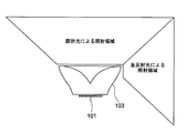
- FIG. 1 is a diagram showing a configuration of a lighting device according to an embodiment of the present invention.
- the illumination device according to the present embodiment includes a surface light source 101 and an optical element 103.
- the surface light source 101 is, for example, a surface emitting LED (Light Emitting Diode) chip alone, or an array of surface emitting LED chips on the surface, OLED (Organic Light-Emitting Diode), LEP (Light Emitting Polymer). ) Etc.
- the surface light source 101 may be circular. Further, when the LED chips are arranged on the surface, the surface may have a curvature. Further, for example, a surface light source on which LED chips are arranged may be sealed with a hemispherical transparent material (for example, silicon resin).
- the optical element 103 has, for example, a shape that is infinitely rotationally symmetric about an axis that passes through the center of the circle of the circular surface light source 101 and is perpendicular to the surface of the surface light source 101. This axis is called the optical axis.
- the incident surface 203 of the optical element 103 faces the light emitting surface 201 of the surface light source 101.
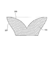
- the optical element 103 further includes a first exit surface 205 facing the entrance surface 203, and a second exit surface 207 that connects the entrance surface 203 and the first exit surface 205 to form a side surface.
- the first emission surface 205 is recessed around the optical axis as compared to the peripheral edge. The shape of the first emission surface 205 will be described in detail later.
- the light emission area of the surface light source 101 is represented by A.
- the light emitting area refers to the area of the arrayed area when, for example, a plurality of LED chips are arrayed.
- the LED chip is sealed with a phosphor or the like, it indicates the area of a region where light is substantially transmitted.
- the total area of the first emission surface 205 and the second emission surface 207 of the optical element 103 is represented by B. Further, the projected area of the first emission surface 205 onto a plane parallel to the surface light source 101 is represented by C.
- the distance in the optical axis direction from the point farthest from the plane including the light emitting surface 201 of the first emission surface 205 to the plane including the light emitting surface 201 is represented by D.
- the depth of the depression of the first emission surface 205 is represented by E.
- the depth E of the dent is the distance in the optical axis direction between the highest point and the lowest point of the first emission surface 205.
- the distance between the light emitting surface 201 and the incident surface 203 is represented by F.
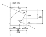
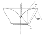
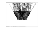
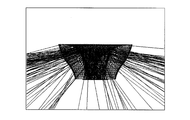
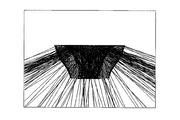
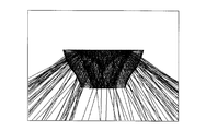
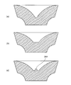
- FIG. 2A is a diagram showing a cross-sectional shape including the optical axis of the optical element 103 according to the present embodiment.
- FIG. 2B is a diagram showing the shape of a figure rotated around the rotation axis (optical axis) in order to obtain a rotationally symmetric body having the cross-sectional shape shown in FIG. 2A.
- the unit of the numbers in FIG. 2B is millimeters.
- the numbers enclosed in FIG. 2B designate the elliptical shape of the cross section of the first exit surface 205. In general, the cross section of the first emission surface 205 may not be elliptical.
- FIG. 2C is a diagram showing the entire ellipse partly shown in FIG. 2B.
- the numbers enclosed in FIGS. 2B and 2C specifically indicate the center position, major axis length, and minor axis length of the ellipse.
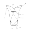
- FIG. 3 is a diagram for explaining the cross-sectional shape of the first emission surface 205 of the optical element 103 including the optical axis.
- the optical element 103 has the shape shown in FIGS. 2A and 2B.
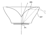
- the intersection of the optical axis and the light emitting surface 201 is defined as a first point P1.
- a point on the circumference of the light emitting surface 201 is defined as a second point P2.
- a point on the first emission surface 205 that is at a prospective angle of 15 degrees from the optical axis with respect to the first point P1 is defined as a third point P3.
- an intersection of a perpendicular standing on the light emitting surface 201 at the second point P2 and a line indicating a cross section of the first emission surface 205 is defined as a fourth point P4.
- the incident angle of the light beam exiting from the first point P1 and reaching the third point P3 to the first exit surface 205 is ⁇ 13 , and the light beam exiting from the second point P2 and reaching the third point P3
- the incident angle on the first exit surface 205 is ⁇ 23
- the incident angle on the first exit surface 205 of the light beam that exits from the first point P 1 and reaches the fourth point P 4 is ⁇ 14
- the second point
- the incident angle of the light ray that has exited from P2 and reaches the fourth point P4 on the first exit surface 205 is ⁇ 24 .
- the following formula is obtained from the geometric relationship.
- the X coordinate of the point farthest from the optical axis of the first exit surface 205 is 10 (millimeter), and the X coordinate of the second point P2 is 4 (millimeter). Therefore, the ratio of the two is 2.5.
- ⁇ 13 is 61.7 °
- ⁇ 14 is 56.0 °.
- the incident angle of the light beam that is emitted from the first point P1 and reaches the region between the third point P3 and the fourth point P4 of the first emission surface 205 to the first emission surface 205. Is greater than the critical angle ⁇ c 39.1 °. Accordingly, the light beam that is emitted from the first point P1 and reaches the region between the third point P3 and the fourth point P4 of the first emission surface 205 is totally reflected by the first emission surface 205. Further, in the present embodiment, the light beam that is emitted from the first point P1 and reaches the entire area outside the third point P3 of the first emission surface 205 is totally reflected by the first emission surface 205. To do.
- theta 23 is 25.8 °
- theta 24 is 29.4 °.
- the first emission surface 205 is An angle with respect to a straight line connecting the first point P1 and the second point P2 is 20 degrees or less.
- the inventor configures the first emission surface 205 as follows, and thus the ratio of the light that is totally reflected by the first emission surface 205 and the light that is refracted out of the light emitted from various points on the surface light source. And the knowledge that light can be irradiated as uniformly as possible not only in the forward direction but also in the lateral and backward directions. That is, in the cross section of the optical element 103 including the optical axis and the second point P2, the first point P1 is the origin, and the axis connecting the first point P1 and the second point P2 is the X axis.
- the light exit surface 205 is an area of 80% or more of the area where the X coordinate is equal to or greater than the value of the third point P3, and the light emitted from the first point P1 is totally reflected, and the X coordinate is the fourth point P4.
- the light emitted from the second point P2 is refracted without being totally reflected in an area of 80% or more of the area that is equal to or less than the value of.
- the ratio of the light that is totally reflected by the first emission surface 205 increases, and the X coordinate of the point that emits light becomes the second value.
- the ratio of light refracted by the first exit surface 205 increases. Therefore, by configuring the first exit surface 205 as described above, the ratio of the light totally reflected by the first exit surface 205 to the refracted light among the light exiting from various points on the surface light source is set. It can be determined appropriately.
- the ratio of the X coordinate of the point farthest from the optical axis of the first emission surface 205 and the X coordinate of the second point P2 is changed. It is possible to further adjust the ratio to the light to be performed. In general, the ratio between the two is preferably 1.5 or more.
- 80% or more area is an “80% or more area” in the X coordinate area. Also, “80% or more area” is intended to exclude some exceptional areas such as the periphery of singular points.
- the rear direction of the light source can be more efficiently achieved. Light can be distributed.
- the shape of the first emission surface 205 can be determined as follows.
- the shape of the first emission surface 205 in the cross section including the optical axis and the second point P2 is referred to as a profile.
- the profile can be represented by a straight line connecting the third point P3 and the fourth point P4.
- the slope of the straight line is determined so that ⁇ 13 and ⁇ 14 are equal to or greater than the critical angle, and ⁇ 24 and ⁇ 24 are smaller than the critical angle. If determined in this way, the incident angle of the light beam incident from the first point P1 to the point on the straight line outside the third point P3 becomes larger than the critical angle, and the light beam is totally reflected. Further, the incident angle of the light beam incident from the second point P2 to the point on the straight line on the optical axis side from the fourth point P4 becomes smaller than the critical angle, and the light beam is refracted.
- the following processing is performed.
- the first point P1 and the second point P2 The ratio at which light rays emitted from any point in between are totally reflected by the first emission surface 205 increases.
- the ratio of the totally reflected light further increases. .
- the following processing is performed to increase the proportion of light that is totally reflected by the first exit surface 205 and irradiated in the backward direction. While satisfying the condition that ⁇ 24 is less than the critical angle, the inclination of the profile near and outside the fourth point P4 with respect to the X axis is reduced, and the X of the point farthest from the optical axis of the first exit surface 205 is reduced. By moving away from the light source while increasing the ratio between the coordinates and the X coordinate of the second point P2, the ratio of the light that is totally reflected by the first exit surface 205 and irradiated in the backward direction increases.
- the following processing is performed. While satisfying the condition that ⁇ 13 is greater than or equal to the critical angle, the inclination of the profile near the third point P3 and the optical axis side with respect to the X axis is reduced, and the first point P1 is emitted. Of the light reaching the region closer to the optical axis than the third point P3 on the exit surface 205, the proportion of light that is refracted increases.
- the ratio of the light totally reflected by the first emission surface 205 and the light refracted is appropriately determined, and the lateral direction and the backward direction as well as the forward direction are determined.
- the following formula needs to be satisfied.
- the gradient of the recess near the optical axis of the first emission surface 205 is too steep, so that the number of rays that pass through in the front direction decreases.
- the ratio of the totally reflected light to the refracted light is not appropriate.
- the gradient of the depression near the optical axis of the first emission surface 205 is too gentle. Therefore, the ratio of the light that is totally reflected and the light that is refracted at the first emission surface 205 is not appropriate. Further, even when the condition of Expression (3) is not satisfied, the ratio of the light that is totally reflected and the light that is refracted on the first emission surface 205 is not appropriate.
- the ratio of the light that is totally reflected and the light that is refracted at the first emission surface 205 becomes more appropriate.
- the shape of the first exit surface 205 near the third point P3 is determined so that the ratio of the totally reflected light to the refracted light becomes more appropriate.
- the ratio of the light that is totally reflected and the light that is refracted at the first emission surface 205 becomes more appropriate.
- the ratio of the size of the optical element to the size of the light source it is preferable that the following expression is satisfied.
- Equations (6) to (9) When each of the terms of Equations (6) to (9) is smaller than the lower limit value, the amount of light traveling in the forward direction of the surface light source increases, and when the value is greater than the upper limit value, the lateral light source moves from the lateral direction to the backward direction. More light goes forward.
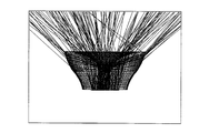
- FIG. 4A is a diagram showing a path of a light beam that is emitted from a point in the vicinity of the first point P1 and reaches the first emission surface 205.
- a light beam emitted from a point near the first point P1 and reaching the region near the optical axis of the first emission surface 205 is refracted without being totally reflected and proceeds forward.
- light rays that are emitted from a point near the first point P1 and reach the region near the optical axis of the first emission surface 205 are totally reflected.
- a light beam emitted from a point near the first point P1 and reaching a region other than the region near the optical axis of the first emission surface 205 is totally reflected and proceeds laterally or backward.
- light rays that are refracted without being totally reflected by the first exit surface 205 are indicated by solid lines, and light rays that are totally reflected are indicated by dotted lines.
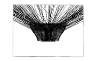
- FIG. 4B is a diagram illustrating a path of a light beam emitted from the second point P2 and reaching the first emission surface 205.
- the light beam that has exited from the second point P2 and reaches the region closer to the optical axis than the fourth point P4 of the first exit surface 205 is refracted and travels forward without being totally reflected.
- a light beam emitted from the second point P ⁇ b> 2 and reaching the peripheral edge of the first emission surface 205 is totally reflected by the first emission surface 205.
- a light beam emitted from the second point P2 and reaching the peripheral edge of the first emission surface 205 may not be totally reflected by the first emission surface 205.
- light rays that are refracted without being totally reflected by the first exit surface 205 are indicated by solid lines, and light rays that are totally reflected are indicated by dotted lines.
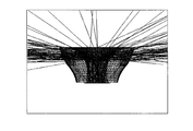
- FIG. 5 is a diagram conceptually showing an irradiation area by refracted light and an irradiation area by total reflection light in the lighting apparatus according to the present embodiment.
- Light emitted from the surface light source 101 and refracted by the first emission surface 205 irradiates in the forward direction.
- the light emitted from the surface light source 101 and totally reflected by the first emission surface 205 irradiates in the lateral and backward directions.
- FIG. 6 is a diagram showing a specific shape of the lighting device 100 according to the present embodiment.
- the surface light source 101 is circular with a radius of 4 millimeters.
- the incident surface 203 of the optical element 103 has a circular shape with a radius of 5.5 millimeters.
- the shape of the optical element 103 is shown in FIGS. 2A and B.
- the optical element 103 is made of a transparent material (for example, epoxy resin) having a refractive index of 1.585. However, in general, any material can be used as the material constituting the optical element as long as it is transparent to the target wavelength.
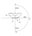
- FIG. 7A is a diagram showing a relative illuminance distribution around the illumination device 100 according to the present embodiment.
- the relative illuminance is on a spherical surface having a radius of 500 millimeters around the center of the light source (a point corresponding to the first point P1).
- the horizontal axis of the graph in FIG. 7A represents an angle with respect to the optical axis, and the vertical axis represents relative illuminance.
- the numerical values of ⁇ 500 to +500 described on the horizontal axis correspond to the position coordinates Y with the light emitting surface 201 as the origin and the optical axis direction as the negative direction, and the numerical values of 0 ° to 180 ° are the light emitting surface 201.
- the relative illuminance in the graph of FIG. 7A shows a value of 1/2 or more of the average value in the range from 0 ° to about 160 ° with respect to the optical axis, and the angle with respect to the optical axis from about 30 ° to about 140 ° In this range, the average value is 2/3 or more.
- FIG. 7B is a diagram for explaining an angle with respect to the optical axis.
- the angle with respect to the optical axis is an angle formed by a straight line extending from the center of the light source with the optical axis.
- the relative illuminance at an angle of 90 ° with respect to the optical axis is relative illuminance at a point where a straight line extending in the horizontal direction from the center of the light source intersects the spherical surface.
- the angle 0 ° with respect to the optical axis is the front direction (front direction) of the surface light source 101
- the angle 180 ° with respect to the optical axis is the back direction (rear direction) of the surface light source 101.
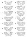
- FIG. 8A to FIG. 8H are diagrams showing the path of the light beam for each irradiation direction.
- FIG. 8A is a diagram showing a path of irradiation light in the forward direction. Most of the light rays are refracted by the first exit surface 205 and travel in the front direction.
- FIG. 8B is a diagram showing a path of irradiation light in a direction that forms an angle smaller than 90 ° with respect to the optical axis. There are light rays that are refracted by the first emission surface 205 and traveling forward, and light rays that are totally reflected by the first emission surface 205 and refracted by the second emission surface 207 and travel forward.
- FIG. 8C is a diagram showing a path of a light beam of irradiation light in a direction smaller than 90 ° with respect to the optical axis and at a larger angle than the case of FIG. 8B.
- About half of the light beam is a light beam that is totally reflected by the first light exit surface 205, refracted by the second light exit surface 207, and travels forward.
- FIG. 8D is a diagram illustrating a path of a light beam of irradiation light in a direction smaller than 90 ° with respect to the optical axis and at a larger angle than in the case of FIG. 8C. Most of the light rays are totally reflected by the first exit surface 205, refracted by the second exit surface 207, and travel forward.
- FIG. 8E is a diagram showing a path of light rays of irradiation light in a direction that forms an angle of approximately 90 ° with respect to the optical axis. Most of the light rays are totally reflected by the first exit surface 205, refracted by the second exit surface 207, and travel in a substantially lateral direction.
- FIG. 8F is a diagram showing a path of irradiation light in a direction that forms an angle larger than 90 ° with respect to the optical axis. Most of the light rays are totally reflected by the first emission surface 205, refracted by the second emission surface 207, and travel backward.
- FIG. 8G is a diagram showing a path of light rays of irradiation light in a direction larger than 90 ° with respect to the optical axis and at a larger angle than in the case of FIG. 8F. Most of the light rays are totally reflected by the first emission surface 205, refracted by the second emission surface 207, and travel backward.
- FIG. 8H is a diagram showing a path of light rays of irradiation light in a direction larger than 90 ° with respect to the optical axis and at a larger angle than in the case of FIG. 8G. Most of the light rays are totally reflected by the first emission surface 205, refracted by the second emission surface 207, and travel backward.
- FIG. 9 is a diagram showing a specific shape (a cross-sectional shape including an optical axis) of an optical element according to another embodiment.
- the curve or the broken line indicating the first emission surface is convex on the side opposite to the surface light source.
- FIG. 10 is a diagram showing a specific shape (a cross-sectional shape including an optical axis) of an optical element according to still another embodiment.
- a part of a curve or a broken line indicating the first emission surface is convex toward the surface light source side.
- FIG. 11 is a diagram showing an embodiment of an optical element in which a light diffusion optical surface 206 is provided in the vicinity of the boundary between the first emission surface 205 and the second emission surface 207 of the optical element.
- a light diffusing optical surface for diffusing light is provided near the boundary of a region where the lens power does not change continuously.
- the optical surface for light diffusion has a concave shape with a constant radius of curvature R, Is preferred. When the upper limit is exceeded, the light diffusing action is reduced.
- FIG. 12 shows various forms near the bottom of the recess of the optical element. For example, as shown in FIG. 12 (c), by providing a protrusion 251 at the bottom of the depression, it is possible to diffuse the light collected near the optical axis.
- FIG. 13 is a diagram illustrating a configuration of a lighting device according to an embodiment of the present invention.
- the illumination device according to the present embodiment includes a surface light source 101 and an optical element 103.
- the light beam emitted from the light emitting surface 201 of the surface light source 101 enters the optical element 103 from the incident surface 203, and the light beam that is more than half of the total light amount of the light source is the first light beam between the incident surface 203 and the first light emitting surface 205.
- the light is guided in the optical axis direction by total reflection on the surface of the second exit surface 208 close to the incident surface 203, thereby forming a virtual light emitting surface 301.
- the virtual light emitting surface 301 has a shape in which the distance from the light emitting surface 201 is H inside the optical element 103 and the light emitting surface 201 is projected onto a plane parallel to 201, and H represents the area of the light emitting surface as A. As And a value in a range in which a light beam having a prospective angle of 15 degrees from the optical axis passing through the center of the virtual light emitting surface exists.
- the light beam that has passed through the virtual light emitting surface 301 is mainly refracted by the first exit surface 205 and is emitted to the outside of the optical element 103, and after being totally reflected by the first exit surface 205, A circuit that is refracted at the exit surface 208 and exits outside the optical element 103 is traced. As a result, a lot of light can be guided in the backward direction of the surface light source 101.
- the optical element is an infinitely rotationally symmetric body.
- the optical element is an infinitely rotationally symmetric body, uniform irradiation is performed radially in the plane perpendicular to the optical axis (rotating axis).
- the optical element does not have to be an infinitely rotationally symmetric body.
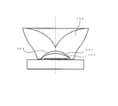
- FIG. 14 is a diagram showing an embodiment of an illumination device in which the surface light source 101 is sealed with a hemispherical transparent sealing member 501.
- the incident surface 203 of the optical element 103 is recessed in a hemispherical shape so that the sealing member 501 and the optical element 103 do not interfere with each other. With such a configuration, even when the surface light source 101 sealed by the transparent sealing member 501 is used, light from the surface light source 101 can be efficiently taken into the optical element 103.
Abstract
照明装置は、面光源(101)と、入射面(203)、第1及び第2の出射面(205,207)を備えた光学素子(103)と、を含む。発光面(201)の中心をP1、縁の点をP2、P1を通り、該発光面に垂直な軸を光軸として、該光学素子は、縁に対して該光軸付近が窪んだ形状を有する。該光学素子の断面において、P1に対して該光軸から15度の見込み角の位置にある第1の出射面上の点をP3、P2から射出して光軸に平行に進む光線が第1の出射面と交差する点をP4、P1とP2とを結ぶ軸をX軸として、第1の出射面の該光軸から最も離れた点のX座標は、P2の値の1.5倍以上であり、第1の出射面は、X座標がP3の値以上である領域の80%以上の領域で、P1から射出した光の入射角が臨界角以上であり、X座標がP4の値以下である領域の80%以上の領域で、P2から射出した光の入射角が臨界角より小さいように構成されている。
Description
本発明は、面光源を使用した照明装置に関する。
最近、輝度が大幅に向上した発光ダイオード(LED)は、エネルギー消費量が小さいことから、従来の白熱電球に代わり、照明装置(LED電球)用の光源として使用され始めている。この際、LED電球の配光分布特性として、従来の白熱電球と同様であることが求められている。
しかし、青色LEDのチップはランバーシアンに近い発光分布特性を有するため、青色LEDと蛍光体を利用した白色もしくは電球色などのLED光源も、ほぼランバーシアンに近い配光分布特性を有する。ここで、ランバーシアンとは、発光強度の観測角に対する分布が、観測角のcos(余弦)に比例する発光分布のことである。したがって、LEDを光源として使用した場合に、白熱灯のように、光が光源の後ろ側に回り込むような照射、すなわち、2π以上の立体角の照射を行うことはできず、また発光面の正面方向の光強度が強くなってしまう。そこで、LEDを使用して、2π以上の立体角に対して、種々の方向に十分な量の光を照射するためには、大きく分けて二つの手段が考えられる。一つ目は、LEDチップを種々の方向に向けて立体的に配置する方法であるが、製造上コストが増し、またLEDの熱設計といった点においても問題が生じる。二つ目は、光源の正面に、光の方向を制御するための光学素子を配置する方法であるが、効率良く理想の配光分布を作り出すような光学素子は存在しなかった。
一方、従来技術において、光源から射出される光の経路を光学素子によって変更する照明装置が開発されている。しかし、従来の照明装置は、点光源を使用したもの(たとえば、特許文献1及び2)か、面光源を使用したものでも、光源の大きさに対して十分に大きな光学素子を用い、コリメート性能を高くするために焦点距離を可能な限り長く設定することで、光を一定の方向に照射するもの(たとえば、特許文献3)であった。
また、一般的に、コリメート以外の(たとえば光線を分散させる)目的であっても、光源の大きさに対して光学素子の大きさが大きければ大きいほど、光線の方向を制御しやすい。これは、光学素子の光学面が、光源から遠い位置にあるほど、光学面上の任意の位置に入射する光線の方向は一意に決まるため、すべての光線を自由に制御できるようになるからである。逆に、光源の大きさに対して光学素子の大きさが同程度である場合、光学素子の光学面は光源の近くにあるため、光学面上の任意の位置に入射する光線の方向は様々な方向を向いており、すべての構成を自由に制御することは不可能である。
このように、光学素子を使用して、LEDなどの面光源から射出された光を2π以上の立体角に対して、種々の方向に十分な量の光を照射するように配光するコンパクトな照明装置は開発されていない。
したがって、光学素子を使用して、LEDなどの面光源から射出された光を2π以上の立体角を照射するように配光するコンパクトな照明装置に対するニーズがある。
本発明の一つの態様による照明装置は、面光源と、該面光源の発光面に対向して配置される入射面、該入射面に対向する第1の出射面及び該入射面と第1の出射面とをつなぐ第2の出射面を備えた光学素子と、を含む。該発光面の中心を第1の点、該発光面の縁の点を第2の点とし、第1の点を通り、該発光面に垂直な軸を該光学素子の光軸として、該光学素子の第1の出射面は、周縁に対して該光軸付近が窪んだ形状を有し、該光軸及び第2の点を含む、該光学素子の断面において、第1の点に対して前記光軸から15度の見込み角の位置にある第1の出射面上の点を第3の点とし、第2の点から射出して光軸に平行に進む光線が第1の出射面と交差する点を第4の点とし、第1の点と第2の点とを結ぶ軸をX軸として、第1の出射面の該光軸から最も離れた点のX座標は、第2の点の値の1.5倍以上であり、第1の出射面は、X座標が第3の点の値以上である領域の80%以上の領域で、第1の点から射出した光の入射角が臨界角以上であり、X座標が第4の点の値以下である領域の80%以上の領域で、第2の点から射出した光の入射角が臨界角より小さいように構成されている。
本態様の照明装置において、第1の出射面のX軸方向の大きさは、発光面のX軸方向の大きさの1.5倍以上である。発光面の第1の点から射出し、第1の出射面の、X座標が第3の点の値以上である領域に至る光の大部分は全反射し、発光面の第2の点から射出し、第1の出射面の、X座標が第4の点の値以下である領域に至る光の大部分は屈折する。発光面の第1の点P1と第2の点P2との間の点から射出した光は、そのX座標によって、第1の出射面で全反射する光及び屈折する光の比率が定まる。一般的に、光を射出する点のX座標が第1の点に近づくと、第1の出射面で全反射する光の比率が高くなり、光を射出する点のX座標が第2の点に近づくと、第1の出射面で屈折する光の比率が高くなる。したがって、第1の出射面を上記のように構成することにより、面光源上の種々の点から射出する光のうち第1の出射面で全反射する光と屈折する光の比率を適切に定めることができる。
なお、本明細書及び特許請求の範囲において、発光面の縁の点とは、光軸を含む断面において、光軸から最も離れた発光面上の点である。
このように本発明は、第1及び第2の点から射出する光の経路に着目して出射面の形状を適切に定め、かつ、面光源のX軸方向の大きさに対する光学素子のX軸方向の大きさの比を適切に定めることにより、面光源から射出された光を2π以上の立体角を照射するように配光するコンパクトな照明装置が得られるという新たな知見に基づくものである。
本発明の一つの態様による照明装置は、面光源と、該面光源の発光面に対向して配置される入射面、該入射面に対向する第1の出射面及び該入射面と第1の出射面とをつなぐ第2の出射面を備えた光学素子と、を含む。該発光面の中心を第1の点、該発光面の縁の点を第2の点とし、第1の点を通り、該発光面に垂直な軸を該光学素子の光軸として、該光学素子の第1の出射面は、周縁に対して該光軸付近が窪んだ形状を有する。該光軸及び第2の点を含む、該光学素子の断面において、第1の出射面が、第1の点に対して該光軸から25度乃至60度の見込み角の領域において、第1の出射面は、第1及び第2の点を結ぶ直線に対する角度が20度以下の角度をなす領域を有し、第1の点に対して前記光軸から15度の見込み角の位置にある第1の出射面上の点を第3の点とし、第2の点から射出して光軸に平行に進む光線が第1の出射面と交差する点を第4の点とし、第1の点から射出して第3の点に至る光線の第1の出射面への入射角をθ13、第2の点から射出して第3の点に至る光線の第1の出射面への入射角をθ23、第1の点から射出して第4の点に至る光線の第1の出射面への入射角をθ14、第2の点から射出して第4の点に至る光線の第1の出射面への入射角をθ24、臨界角をθcとして、

である。
式(1)乃至(3)が満たされることにより、第1の出射面において、全反射する光と屈折する光の比率が適切に定められ、前方方向のみならず横方向及び後方方向に一様に光を照射することができる。
本発明の一つの実施形態において、さらに

である。
本実施形態によれば、第1の出射面において、全反射する光と屈折する光の比率がより適切になる。
本発明の一つの実施形態において、該光軸及び第2の点を含む、該光学素子の断面において、第1の点と第2の点とを結ぶ軸をX軸として、X座標が第3の点の値以上の領域において、第1の出射面は、第1の点から射出する光をすべて全反射させるように構成されている。
本実施形態によれば、前方方向のみならず横方向及び後方方向により一様に光を照射することができる。
本発明の一つの実施形態において、該光軸及び第2の点を含む、該光学素子の断面において、第1の点と第2の点とを結ぶ軸をX軸として、X軸方向の第3の点と第4の点との間の領域において、第1の出射面は、第2の点から射出する光をすべて屈折させるように構成されている。
本実施形態によれば、前方方向のみならず横方向及び後方方向により一様に光を照射することができる。
本発明の一つの実施形態において、該光軸及び第2の点を含む、該光学素子の断面において、第1の点と第2の点とを結ぶ軸をX軸として、X軸方向の第3の点と第4の点との間の領域において、第1の出射面は、第3の点と第4の点とを結ぶ直線に関して、該面光源の反対側に位置する。
本実施形態によれば、前方方向のみならず横方向及び後方方向により一様に光を照射することができる。
本発明の一つの実施形態において、該発光面の面積をAとし、第1の出射面の面積をBとして、

である。
本実施形態によれば、前方方向のみならず横方向及び後方方向により一様に光を照射することができる。
本発明の一つの実施形態において、該発光面の面積をAとし、第1の出射面の該面光源と平行な面への射影面積をCとして、

である。
本実施形態によれば、前方方向のみならず横方向及び後方方向により一様に光を照射することができる。
本発明の一つの実施形態において、該発光面の面積をAとし、該光学素子の高さをDとして、

である。
本実施形態によれば、前方方向のみならず横方向及び後方方向により一様に光を照射することができる。
本発明の一つの実施形態において、該発光面の面積をAとし、第1の出射面の窪みの深さをEとして、

である。
本実施形態によれば、前方方向のみならず横方向及び後方方向により一様に光を照射することができる。
本発明の一つの実施形態において、第1の出射面が、該第3の点より該光軸に近い領域に、光拡散のための突起構造を備えている。
本実施形態によれば、光軸付近に集まる光線を拡散させることができる。
本発明の一つの実施形態において、該発光面と該入射面とが間隔を隔てて分離されている。
本実施形態によれば、該入射面における光の屈折を利用でき、光線制御の自由度が増す。
本発明の一つの実施形態において、該発光面の面積をAとし、該発光面と該入射面との間隔をFとして、

である。
本実施形態によれば、入射面に取り込まれる光線の割合を最大限に確保することができる。
本発明の一つの実施形態において、該光軸及び第2の点を含む、該光学素子の断面において、第1の点と第2の点とを結ぶ軸をX軸として、第1の出射面のXに関する導関数が連続である。
本実施形態によれば、光線ムラを抑えることができる。
本発明の一つの実施形態において、第1の出射面及び第2の出射面の少なくとも一部の領域に微小凹凸形状を施している。
本実施形態によれば、より一様に光を照射することができる。
本発明の一つの実施形態において、該光軸及び第2の点を含む、該光学素子の断面において、第2の出射面が直線状の部分を有する。
本実施形態による照明装置の光学素子は、第1の出射面と第2の出射面との境界付近に発生しやすい光線ムラを抑えることができる。
本発明の一つの実施形態において、該光学素子が、第1の出射面及び第2の出射面の境界付近に光拡散用光学面を備えている。
本実施形態によれば、第1の出射面と第2の出射面との境界付近に発生しやすい光線ムラを抑えることができる。
本発明の一つの実施形態において、該光拡散用光学面が、曲率半径Rの凹形状であり、該発光面の面積をAとして、

である。
本実施形態による照明装置の光学素子の光拡散用光学面は、十分な光拡散機能を有する。
本発明の一つの実施形態において、該光学素子が、第1の出射面及び第2の出射面の境界付近に、外側に延びた導光部を備えている。
本実施形態において、導光部は第1の出射面と第2の出射面との境界付近に発生しやすい光線ムラを抑える機能を果たす。
本発明の一つの実施形態において、該光源および該光学素子を覆うカバーを備え、該カバーが該導光部によって該光学素子に接続されている。
本実施形態によれば、第1の出射面と第2の出射面との境界付近に発生しやすい光線ムラを抑えながら、光源からの熱の問題を解決した照明装置が得られる。
本発明の一つの実施形態において、該光学素子が、該光軸を中心とする無限回回転対称体である。
本実施形態によれば、該光軸に垂直な断面内において、該光軸を中心とする各放射方向に一様な照射を行うことができる。
本発明の一つの実施形態において、該光軸の周囲の回転対称な形状から、180°以下の扇形に切り出した部分を利用している。
本実施形態によれば、用途に合わせてより適切な形状の照明装置が得られる。
本発明の一つの実施形態において、該光軸の周囲の回転対称な形状から、180°以下の扇形に切り出した部分を利用し、該光学素子の切断面が曲面である。
本実施形態によれば、用途に合わせてより適切な形状の照明装置が得られる。
本発明の一つの実施形態において、該光学素子の該光軸に垂直な断面の形状が、該光軸を中心とする放射方向によって異なる照射を行なうように放射方向によって異なるように構成されている。
本実施形態によれば、該光軸に垂直な断面内において、該光軸を中心とする放射方向によって異なる照射を行なうことができる。
本発明の一つの態様による照明装置は、面光源と、該面光源の発光面に対向して配置される入射面、該入射面に対向する第1の出射面及び該入射面と第1の出射面とをつなぐ第2の出射面を備えた光学素子と、を含む照明装置であって、第2の出射面の該入射面に近い領域は、該発光面に対して垂直の方向から外れた方向に射出された光線の一部を内部全反射により導光することで、該光学素子内部において、該発光面からの距離がHであり、該発光面に平行な平面に該発光面を投射した形状の仮想発光面を形成するように構成され、Hは、該発光面の面積をAとして、

を満たし、該仮想発光面の中心を通過する前記光軸から15度の見込み角の光線が存在する範囲の値であり、該仮想発光面の中心を第1の点、該仮想発光面の縁の点を第2の点とし、第1の点を通り、該仮想発光面に垂直な軸を該光学素子の光軸として、該光学素子の第1の出射面は、周縁に対して該光軸付近が窪んだ形状を有し、該光軸及び第2の点を含む、該光学素子の断面において、第1の点に対して前記光軸から15度の見込み角の位置にある第1の出射面上の点を第3の点とし、第2の点を通過して光軸に平行に進む光線が第1の出射面と交差する点を第4の点とし、第1の点を原点とし、第1の点と第2の点とを結ぶ軸をX軸として、第1の出射面の該光軸から最も離れた点のX座標は、第2の点の値の1.5倍以上であり、第1の出射面は、X座標が第3の点の値以上である領域の80%以上の領域で、第1の点を通過した光の入射角が臨界角以上であり、X座標が第4の点の値以下である領域の80%以上の領域で、第2の点を通過した光の入射角が臨界角より小さいように構成された照明装置。
本態様の照明装置において、該光源から離れた高い位置で後方方向に光線を向けることができ、該光源の後方方向に多くの光を導くことが可能となる。
本発明の一つの態様による照明装置は、面光源と、該面光源の発光面に対向して配置される入射面、該入射面に対向する第1の出射面及び該入射面と第1の出射面とをつなぐ第2の出射面を備えた光学素子と、を含む照明装置であって、第2の出射面の該入射面に近い領域は、該発光面に対して垂直の方向から外れた方向に射出された光線の一部を内部全反射により導光することで、該光学素子内部において、該発光面からの距離がHであり、該発光面に平行な平面に該発光面を投射した形状の仮想発光面を形成するように構成され、Hは、該発光面の面積をAとして、

を満たし、該仮想発光面の中心を通過する前記光軸から15度の見込み角の光線が存在する範囲の値であり、該仮想発光面の中心を第1の点、該仮想発光面の縁の点を第2の点とし、第1の点を通り、該仮想発光面に垂直な軸を該光学素子の光軸として、該光学素子の第1の出射面は、周縁に対して該光軸付近が窪んだ形状を有し、該光軸及び第2の点を含む、該光学素子の断面において、第1の点に対して該光軸から25度乃至60度の見込み角の領域において、第1の出射面は、第1及び第2の点を結ぶ直線に対する角度が20度以下の角度をなす領域を有し、第1の点に対して前記光軸から15度の見込み角の位置にある第1の出射面上の点を第3の点とし、第2の点を通過して光軸に平行に進む光線が第1の出射面と交差する点を第4の点とし、第1の点と第3の点を通る線分と、第2の点と第3の点を通る線分が成す角度をθ132、第1の点と第4の点を通る線分と、第2の点と第4の点を通る線分が成す角度をθ142、臨界角をθcとして、

である照明装置。
本態様の照明装置において、該光源から離れた高い位置で後方方向に光線を向けることができ、該光源の後方方向に多くの光を導くことが可能となる。
図1は、本発明の一実施形態による照明装置の構成を示す図である。本実施形態による照明装置は、面光源101と光学素子103とを含む。面光源101は、たとえば、面発光タイプのLED(Light Emitting Diode)チップ単体、また、面発光タイプのLEDチップを面上に配列したもの、OLED(Organic Light-Emitting Diode)、LEP(Light Emitting Polymer)などである。面光源101は、円形であってもよい。また、LEDチップを面上に配列する場合、該面は曲率を有していてもよい。また、たとえば、LEDチップを配列した面光源が半球状の透明な材料(たとえば、シリコン樹脂など)で封止されたものであってもよい。光学素子103は、たとえば、円形の面光源101の円の中心を通り、面光源101の面に垂直な軸に関して無限回回転対称な形状を有する。この軸を光軸と呼称する。
光学素子103の入射面203は、面光源101の発光面201に対向している。光学素子103は、入射面203に対向する第1の出射面205と、入射面203及び第1の出射面205をつなぎ、側面を構成する第2の出射面207をさらに含む。第1の出射面205は、周縁部に比較して光軸周辺が窪んでいる。第1の出射面205の形状については後で詳細に説明する。
面光源101の発光面積をAであらわす。ここで、発光面積とは、たとえば、複数のLEDチップを配列した場合は、その配列されている領域の面積を指す。また、LEDチップが蛍光体などで封止されている場合は、実質的に光線が通過しているとされる領域の面積を指す。本実施形態においては、面光源101は、半径r及び面積A(=πr2)の円形の発光面を備える。
光学素子103の第1の出射面205及び第2の出射面207の面積の合計をBで表す。また、第1の出射面205の、面光源101に平行な平面への射影面積をCで表す。
第1の出射面205の、発光面201を含む平面から最も離れた点から発光面201を含む平面までの光軸方向の距離をDで表す。
第1の出射面205の、窪みの深さをEで表す。図1において、窪みの深さEは、第1の出射面205の最も高い位置の点と最も低い位置の点との光軸方向の距離である。
発光面201と入射面203との間隔をFで表す。
図2Aは、本実施形態による光学素子103の光軸を含む断面形状を示す図である。
図2Bは、図2Aに示された断面形状を有する回転対称体を得るために、回転軸(光軸)の周囲に回転させる図形の形状を示す図である。図2Bの数字の単位はミリメータである。図2Bにおいて囲われた数字は、第1の出射面205の断面の楕円形状を指定するものである。一般的に、第1の出射面205の断面は、楕円形状でなくともよい。
図2Cは、図2Bに一部が示された楕円の全体を示す図である。図2B及び図2Cにおいて囲われた数字は、具体的に楕円の中心位置、長軸長さ及び短軸長さを示す。
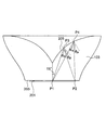
図3は、光学素子103の第1の出射面205の、光軸を含む断面の形状を説明するための図である。光学素子103は、図2A及び図2Bに示した形状を有するものとする。図3において、光軸と発光面201との交点を第1の点P1とする。また、発光面201の円周上の点を第2の点P2とする。さらに、第1の点P1に対して光軸から15度の見込み角の位置にある第1の出射面205上の点を第3の点P3とする。さらに、第2の点P2において発光面201に立てた垂線と第1の出射面205の断面を示す線との交点を第4の点P4とする。
第1の点P1から射出して第3の点P3に至る光線の第1の出射面205への入射角をθ13、第2の点P2から射出して第3の点P3に至る光線の第1の出射面205への入射角をθ23、第1の点P1から射出して第4の点P4に至る光線の第1の出射面205への入射角をθ14、第2の点P2から射出して第4の点P4に至る光線の第1の出射面205への入射角をθ24とする。面光源101の半径は、r=4(ミリメータ)、臨界角は、θc=39.1°である。ここで、幾何学的関係から以下の式が得られる。
(1)θ13-θ23 = 35.9°
(2)θ14-θ24 = 26.6°
(3)(θ14-θ24)/(θ13-θ23) = 0.74
(4)θ13 = 61.7°
(5)θ23 = 25.8°
(6)B/A = 17.08
(7)C/A = 6.25
(8)D/r = 2.38
(9)E/r = 1.48
(10)F/r = 0.025
(2)θ14-θ24 = 26.6°
(3)(θ14-θ24)/(θ13-θ23) = 0.74
(4)θ13 = 61.7°
(5)θ23 = 25.8°
(6)B/A = 17.08
(7)C/A = 6.25
(8)D/r = 2.38
(9)E/r = 1.48
(10)F/r = 0.025
第1の出射面205の光軸から最も離れた点のX座標は、10(ミリメータ)であり、第2の点P2のX座標は、4(ミリメータ)である。したがって、両者の比は、2.5である。
θ13は、61.7°であり、θ14は、56.0°である。このように、第1の点P1から射出して、第1の出射面205の第3の点P3と第4の点P4の間の領域に至る光線の第1の出射面205への入射角は、臨界角θc=39.1°よりも大きい。したがって、第1の点P1から射出して、第1の出射面205の第3の点P3と第4の点P4の間の領域に至る光線は、第1の出射面205で全反射する。さらに、本実施形態において、第1の点P1から射出して、第1の出射面205の、第3の点P3よりも外側の全領域に至る光線は、第1の出射面205で全反射する。
θ23は、25.8°であり、θ24は、29.4°である。このように、第2の点P2から射出して、第1の出射面205の第3の点P3と第4の点P4の間の領域に至る光線の第1の出射面205への入射角は、臨界角θc=39.1°よりも小さい。したがって、第2の点P2から射出して、第1の出射面205の第3の点P3と第4の点P4の間の領域に至る光線は、第1の出射面205で全反射することなく屈折する。さらに、本実施形態において、第2の点P2から射出して、第1の出射面205の、第4の点P4よりも光軸側の全領域に至る光線は、第1の出射面205で全反射することなく屈折する。
光軸及び第2の点を含む、光学素子103の断面において、第1の点に対して光軸から25度以上の見込み角の少なくとも一部の領域において、第1の出射面205は、第1点P1及び第2の点P2を結ぶ直線に対する角度が20度以下である。
発明者は、第1の出射面205を以下のように構成することによって、面光源上の種々の点から射出する光のうち第1の出射面205で全反射する光と屈折する光の比率を適切に定め、前方方向のみならず横方向及び後方方向にできるだけ一様に光を照射することができるとの知見を得た。すなわち、光軸及び第2の点P2を含む、光学素子103の断面において、第1の点P1を原点、第1の点P1と第2の点P2とを結ぶ軸をX軸として、第1の出射面205は、X座標が第3の点P3の値以上である領域の80%以上の領域で、第1の点P1から射出した光が全反射し、X座標が第4の点P4の値以下である領域の80%以上の領域で、第2の点P2から射出した光が全反射することなく屈折するように構成する。このように構成すると、発光面201の第1の点P1から射出し、第1の出射面205の第3の点P3より外側の領域に至る光線の大部分は、第1の出射面205で全反射し、発光面201の第2の点P2から射出し、第1の出射面205の第4の点P4より光軸側の領域に至る光線の大部分は、第1の出射面205で屈折する。発光面201の第1の点P1と第2の点P2との間の点から射出し、第1の出射面205に至る光線は、そのX座標によって、第1の出射面205で全反射する光及び屈折する光の比率が定まる。一般的に、光を射出する点のX座標が第1の点P1に近づくと、第1の出射面205で全反射する光の比率が高くなり、光を射出する点のX座標が第2の点P2に近づくと、第1の出射面205で屈折する光の比率が高くなる。したがって、上記のように第1の出射面205を構成することにより、面光源上の種々の点から射出する光のうち第1の出射面205で全反射する光と屈折する光との比率を適切に定めることができる。
また、第1の出射面205の光軸から最も離れた点のX座標と、第2の点P2のX座標との比を変えることによって、第1の出射面205で全反射する光と屈折する光との比率をさらに調整することができる。一般的に、両者の比は1.5以上であるのが好ましい。
ここで、「80%以上の領域」とは、X座標の領域で「80%以上の領域」である。また、「80%以上の領域」としたのは、特異点の周辺など一部の例外的領域を除く趣旨である。
さらには、第1の出射面205の光軸から最も離れた点のX座標と、第2の点P2のX座標との比が2.0以上であれば、より効率よく光源の後方方向まで光を分布させることができる。
一般的に、第1の出射面205の形状は、以下のように定めることができる。ここで、光軸及び第2の点P2を含む断面における第1の出射面205の形状をプロファイルと呼称する。最初に、プロファイルは、第3の点P3及び第4の点P4を結ぶ直線で表せるとする。θ13及びθ14が臨界角以上となり、θ24及びθ24が臨界角より小さくなるように直線の傾きを定める。このように定めると、第1の点P1から、第3の点P3より外側の直線上の点に入射する光線の入射角は臨界角より大きくなり、光線は全反射する。また、第2の点P2から、第4の点P4より光軸側の直線上の点に入射する光線の入射角は臨界角より小さくなり、光線は屈折する。
第1の出射面205で全反射する光の割合を増加させるには以下の処理を行う。第2の点P2から射出して第4の点P4に向かう光線の、第1の出射面205への入射角が大きくなるようにすることによって、第1の点P1と第2の点P2の間の任意の点から射出した光線が、第1の出射面205で全反射する割合が増加する。また、第1の出射面205の光軸から最も離れた点のX座標と、第2の点P2のX座標との比を増加させることにより、上記の全反射する光の割合はさらに増加する。
第1の出射面205で全反射して後方方向へ照射される光の割合を増加させるには以下の処理を行う。θ24が臨界角未満である条件を満たしながら、第4の点P4付近及びそれより外側のプロファイルのX軸に対する傾きを小さくし、第1の出射面205の光軸から最も離れた点のX座標と、第2の点P2のX座標との比を増加させながら光源から遠ざけることにより、第1の出射面205で全反射して後方方向へ照射される光の割合は増加する。
第1の出射面205で屈折する光の割合を増加させるには以下の処理を行う。θ13が臨界角以上である条件を満たしながら、第3の点P3付近及びそれより光軸側のプロファイルのX軸に対する傾きを小さくすることによって、第1の点P1から射出され、第1の出射面205の、第3の点P3より光軸側の領域に至る光の内、屈折する光の割合が増加する。
また、別の観点から面光源上の種々の点から射出する光のうち第1の出射面205で全反射する光と屈折する光の比率を適切に定め、前方方向のみならず横方向及び後方方向にできるだけ一様に光を照射するには、以下の式が満たされる必要がある。

式(1)の上限を上回るか式(2)の下限を下回る範囲においては、第1の出射面205の光軸付近の窪みの勾配が急すぎるため、正面方向に抜ける光線が少なくなってしまい、第1の出射面205において、全反射する光と屈折する光の比率が適切にならない。また、式(1)の下限を下回るか式(2)の上限を上回る範囲においては、第1の出射面205の光軸付近の窪みの勾配が緩やかすぎるため、ほとんどの光線が正面方向に抜けてしまい、第1の出射面205において、全反射する光と屈折する光の比率が適切にならない。また、式(3)の条件が満たされない場合も、第1の出射面205において、全反射する光と屈折する光の比率が適切にならない。
さらに、

であれば、第1の出射面205において、全反射する光と屈折する光の比率がより適切になる。
さらに、

であれば、第1の出射面205において、全反射する光と屈折する光の比率がより適切になるように、第1の出射面205の第3の点P3付近の形状が定められる。
さらに、

であれば、第1の出射面205において、全反射する光と屈折する光との比率がより適切になる。
さらに、光源の大きさに対する光学素子の大きさの比に関しては、以下の式が満たされるのが好ましい。

式(6)乃至式(9)の各項が下限値より小さな値になると、面光源の前方方向に進む光が多くなり、上限値より大きな値となると、面光源の横方向から後方方向に進む光が多くなる。
さらに、

であれば、より好ましい配光分布となる。
さらに、以下の式が満たされるのが好ましい。

式(10)の項が上限値より大きな値となると、入射面203に取り込まれる光線の割合が低下する。
図4Aは、第1の点P1の近傍の点から射出して、第1の出射面205に至る光線の経路を示す図である。図4Aにおいて、第1の点P1の近傍の点から射出して、第1の出射面205の光軸付近の領域に至る光線は全反射することなく屈折して前方へ進む。ただし、一般的には、第1の点P1の近傍の点から射出して、第1の出射面205の光軸付近の領域に至る光線は全反射する場合もある。第1の点P1の近傍の点から射出して、第1の出射面205の光軸付近の領域以外の領域に至る光線は全反射して横方向または後方へ進む。図4Aにおいて、第1の出射面205で全反射することなく屈折する光線を実線で示し、全反射する光線を点線で示した。
図4Bは、第2の点P2から射出して、第1の出射面205に至る光線の経路を示す図である。図4Bにおいて、第2の点P2から射出して、第1の出射面205の第4の点P4より光軸に近い領域に至る光線は、全反射することなく屈折して前方へ進む。第2の点P2から射出して、第1の出射面205の周縁部に至る光線は第1の出射面205で全反射する。ただし、一般的には、第2の点P2から射出して、第1の出射面205の周縁部に至る光線は第1の出射面205で全反射しない場合もある。図4Bにおいて、第1の出射面205で全反射することなく屈折する光線を実線で示し、全反射する光線を点線で示した。
図5は、本実施形態による照明装置において、屈折光による照射領域及び全反射光による照射領域を概念的に示す図である。面光源101から射出して、第1の出射面205で屈折した光は、前方方向を照射する。面光源101から射出して、第1の出射面205で全反射した光は、側方及び後方方向を照射する。
図6は、本実施形態による照明装置100の具体的な形状を示す図である。面光源101は、半径4ミリメータの円形である。光学素子103の入射面203は、半径5.5ミリメータの円形である。光学素子103の形状は、図2A及び図Bに示したものである。光学素子103は、屈折率1.585の透明材料(たとえば、エポキシ樹脂)から構成される。ただし、一般的には、光学素子を構成する材料としては、対象とする波長に対して透明であればどのようなものでも使用することができる。
図7Aは、本実施形態による照明装置100の周囲の相対照度分布を示す図である。相対照度は、光源の中心(第1の点P1に相当する点)を中心とした半径500ミリメータの球面上のものである。図7Aのグラフの横軸は、光軸に対する角度を表し、縦軸は相対照度を表す。また、横軸に記載されている-500乃至+500の数値は、発光面201を原点として光軸方向を負方向とした位置座標Yに対応し、0°乃至180°の数値は、発光面201を原点とした半径500ミリメータの球面上で、位置座標Yに対応する点を原点から見た際の、光軸方向からの角度θであり、θ=360/(2π)×cos-1(-Y/500)の関係がある。図7Aのグラフの相対照度は、光軸に対する角度が0°から約160°までの範囲で、平均値の1/2以上の値を示し、光軸に対する角度が約30°から約140°までの範囲で、平均値の2/3以上の値を示している。
図7Bは、光軸に対する角度を説明するための図である。光軸に対する角度とは、光源の中心から延びる直線が光軸となす角度である。たとえば、光軸に対する角度90°の相対照度とは、光源の中心から水平方向に延びる直線が、上記の球面と交差する点における相対照度である。光軸に対する角度0°は、面光源101の正面方向(前方方向)であり、光軸に対する角度180°は、面光源101の裏面方向(後方方向)である。
図8A乃至図8Hは、照射方向ごとに光線の経路を示した図である。
図8Aは、前方方向の照射光の経路を示す図である。ほとんどの光線は、第1の出射面205で屈折して正面方向に進む。
図8Bは、光軸に対して90°より小さなある角度をなす方向の照射光の経路を示す図である。第1の出射面205で屈折して前方に進む光線と、第1の出射面205で全反射し、第2の出射面207で屈折して前方に進む光線とが存在する。
図8Cは、光軸に対して90°より小さく、図8Bの場合よりも大きな角度をなす方向の照射光の光線の経路を示す図である。光線の約半分は、第1の出射面205で全反射し、第2の出射面207で屈折して前方に進む光線である。
図8Dは、光軸に対して90°より小さく、図8Cの場合よりも大きな角度をなす方向の照射光の光線の経路を示す図である。光線のほとんどは、第1の出射面205で全反射し、第2の出射面207で屈折して前方に進む光線である。
図8Eは、光軸に対してほぼ90°の角度をなす方向の照射光の光線の経路を示す図である。光線のほとんどは、第1の出射面205で全反射し、第2の出射面207で屈折してほぼ横方向に進む光線である。
図8Fは、光軸に対して90°より大きなある角度をなす方向の照射光の経路を示す図である。光線のほとんどは、第1の出射面205で全反射し、第2の出射面207で屈折して後方に進む光線である。
図8Gは、光軸に対して90°より大きく、図8Fの場合よりも大きな角度をなす方向の照射光の光線の経路を示す図である。光線のほとんどは、第1の出射面205で全反射し、第2の出射面207で屈折して後方に進む光線である。
図8Hは、光軸に対して90°より大きく、図8Gの場合よりも大きな角度をなす方向の照射光の光線の経路を示す図である。光線のほとんどは、第1の出射面205で全反射し、第2の出射面207で屈折して後方に進む光線である。
図9は、他の実施形態による光学素子の具体的な形状(光軸を含む断面形状)を示す図である。図9に示した実施形態では、第1の出射面を示す曲線または折れ線が、面光源と反対側に凸となっている。
図10は、さらに他の実施形態による光学素子の具体的な形状(光軸を含む断面形状)を示す図である。図10に示した実施形態では、第1の出射面を示す曲線または折れ線の一部が、面光源側に凸となっている。
図11は、光学素子の第1の出射面205と第2の出射面207との境界付近に光拡散用光学面206を設けた光学素子の実施形態を示す図である。経路の異なる光線が干渉する領域では光線ムラが発生しやすい。そこで、この光線ムラを緩和する手段として、レンズパワーが連続に変化しない領域の境界付近に光を拡散させるための光拡散用光学面を設けた。光拡散用光学面は一定の曲率半径Rの凹形状であり、

であるのが好ましい。上限値を超えた場合には、光拡散作用が小さくなる。
図12は、光学素子の窪みの底部付近の種々の形態を示す図である。たとえば、図12(c)に示すように、窪みの底部に突起物251を設けることにより、光軸付近に集まる光線を拡散させることができる。
図13は、本発明の一実施形態による照明装置の構成を示す図である。本実施形態による照明装置は、面光源101と光学素子103とを含む。面光源101の発光面201から射出した光線は、入射面203から光学素子103に入射し、光源の全光量の半分以上の光線は、入射面203と第1の出射面205との間の第2の射出面208の入射面203に近い側の面での全反射により、光軸方向に導光され、仮想発光面301を形成する。仮想発光面301は、光学素子103の内部において、発光面201からの距離がHであり、201に平行な平面に発光面201を投射した形状であり、Hは、該発光面の面積をAとして、

を満たし、該仮想発光面の中心を通過する前記光軸から15度の見込み角の光線が存在する範囲の値である。仮想発光面301を通過した光線は主に、第1の射出面205で屈折し、光学素子103の外部に射出される経路と、第1の射出面205で全反射された後、第2の射出面208で屈折し、光学素子103の外部に射出される回路を辿る。これにより、面光源101の後方方向に多くの光を導くことが可能となる。
上記の実施形態において、光学素子は、無限回回転対称体である。光学素子が、無限回回転対称体である場合には、光軸(回転軸)と垂直な面内において、光軸を中心として放射状に一様な照射が行なわれる。しかし、一般的に、光学素子は、無限回回転対称体である必要はない。光軸を含む断面において上記の条件を満たしながら、光軸の周りの角度によって形状を変化させることにより、光軸の周りの角度によって異なった照射を行うことができる。
図14は、面光源101が半球状の透明な封止部材501により封止されている照明装置の実施形態を示す図である。封止部材501と光学素子103とが干渉しないように、光学素子103の入射面203は、半球状に窪んでいる。このような構成により、透明な封止部材501により封止されている面光源101を使用する場合でも、面光源101からの光を効率よく光学素子103に取り込むことができる。
Claims (26)
- 面光源と、該面光源の発光面に対向して配置される入射面、該入射面に対向する第1の出射面及び該入射面と第1の出射面とをつなぐ第2の出射面を備えた光学素子と、を含む照明装置であって、
該発光面の中心を第1の点、該発光面の縁の点を第2の点とし、第1の点を通り、該発光面に垂直な軸を該光学素子の光軸として、該光学素子の第1の出射面は、周縁に対して該光軸付近が窪んだ形状を有し、該光軸及び第2の点を含む、該光学素子の断面において、第1の点に対して前記光軸から15度の見込み角の位置にある第1の出射面上の点を第3の点とし、第2の点から射出して光軸に平行に進む光線が第1の出射面と交差する点を第4の点とし、第1の点を原点とし、第1の点と第2の点とを結ぶ軸をX軸として、第1の出射面の該光軸から最も離れた点のX座標は、第2の点の値の1.5倍以上であり、第1の出射面は、X座標が第3の点の値以上である領域の80%以上の領域で、第1の点から射出した光の入射角が臨界角以上であり、X座標が第4の点の値以下である領域の80%以上の領域で、第2の点から射出した光の入射角が臨界角より小さいように構成された照明装置。 - 面光源と、該面光源の発光面に対向して配置される入射面、該入射面に対向する第1の出射面及び該入射面と第1の出射面とをつなぐ第2の出射面を備えた光学素子と、を含む照明装置であって、
該発光面の中心を第1の点、該発光面の縁の点を第2の点とし、第1の点を通り、該発光面に垂直な軸を該光学素子の光軸として、該光学素子の第1の出射面は、周縁に対して該光軸付近が窪んだ形状を有し、該光軸及び第2の点を含む、該光学素子の断面において、第1の点に対して該光軸から25度乃至60度の見込み角の領域において、第1の出射面は、第1及び第2の点を結ぶ直線に対する角度が20度以下の角度をなす領域を有し、第1の点に対して前記光軸から15度の見込み角の位置にある第1の出射面上の点を第3の点とし、第2の点から射出して光軸に平行に進む光線が第1の出射面と交差する点を第4の点とし、第1の点から射出して第3の点に至る光線の第1の出射面への入射角をθ13、第2の点から射出して第3の点に至る光線の第1の出射面への入射角をθ23から射出して第4の点に至る光線の第1の出射面への入射角をθ24、臨界角をθcとして、

- さらに

- 該光軸及び第2の点を含む、該光学素子の断面において、第1の点と第2の点とを結ぶ軸をX軸として、X座標が第3の点の値以上の領域において、第1の出射面は、第1の点から射出する光をすべて全反射させるように構成された請求項1から3のいずれかに記載の照明装置。
- 該光軸及び第2の点を含む、該光学素子の断面において、第1の点と第2の点とを結ぶ軸をX軸として、X軸方向の第3の点と第4の点との間の領域において、第1の出射面は、第2の点から射出する光をすべて屈折させるように構成された請求項1から3のいずれかに記載の照明装置。
- 該光軸及び第2の点を含む、該光学素子の断面において、第1の点と第2の点とを結ぶ軸をX軸として、X軸方向の第3の点と第4の点との間の領域において、第1の出射面は、第3の点と第4の点とを結ぶ直線に関して、該面光源の反対側に位置する請求項1から3のいずれかに記載の照明装置。
- 該発光面の面積をAとし、第1の出射面の面積をBとして、

- 該発光面の面積をAとし、第1の出射面の該光源面への射影面積をCとして、

- 該発光面の面積をAとし、該光学素子の高さをDとして、

- 該発光面の面積をAとし、第1の出射面の窪みの深さをEとして、

- 第1の出射面が、該第3の点より該光軸に近い領域に、光拡散のための突起構造を備えた請求項1から10のいずれかに記載の照明装置。
- 該発光面と該入射面とが間隔を隔てて分離されている請求項1から11のいずれかに記載の照明装置。
- 該発光面の面積をAとし、該発光面と該入射面との間隔をFとして、

- 該光軸及び第2の点を含む、該光学素子の断面において、第1の点と第2の点とを結ぶ軸をX軸として、第1の出射面のXに関する導関数が連続である請求項1から13のいずれかに記載の照明装置。
- 第1の出射面及び第2の出射面の少なくとも一部の領域に微小凹凸形状を施した請求項1から14のいずれかに記載の照明装置。
- 該光軸及び第2の点を含む、該光学素子の断面において、第2の出射面が直線状の部分を有する請求項1から15のいずれかに記載の照明装置。
- 該光学素子が、第1の出射面及び第2の出射面の境界付近に光拡散用光学面を備えた請求項16に記載の照明装置。
- 該光拡散用光学面が、曲率半径Rの凹形状であり、該発光面の面積をAとして、

- 該光学素子が、第1の出射面及び第2の出射面の境界付近に、外側に延びた導光部を備えた請求項16に記載の照明装置。
- 該光源および該光学素子を覆うカバーを備え、該カバーが該導光部によって該光学素子に接続された請求項19に記載の照明装置。
- 該光学素子が、該光軸を中心とする無限回回転対称体である請求項1から20のいずれかに記載の照明装置。
- 該光軸の周囲の回転対称な形状から、180°以下の扇形形状に切り出した部分を利用した請求項21に記載の照明装置。
- 該光学素子の、該扇形形状に切り出した切断面が曲面である請求項22に記載の照明装置。
- 該光学素子の該光軸に垂直な断面の形状が、該光軸を中心とする放射方向によって異なる照射を行なうように、放射方向によって異なるように構成された請求項1から20のいずれかに記載の照明装置。
- 面光源と、該面光源の発光面に対向して配置される入射面、該入射面に対向する第1の出射面及び該入射面と第1の出射面とをつなぐ第2の出射面を備えた光学素子と、を含む照明装置であって、
第2の出射面の該入射面に近い領域は、該発光面に対して垂直の方向から外れた方向に射出された光線の一部を内部全反射により導光することで、該光学素子内部において、該発光面からの距離がHであり、該発光面に平行な平面に該発光面を投射した形状の仮想発光面を形成するように構成され、Hは、該発光面の面積をAとして、

該仮想発光面の中心を第1の点、該仮想発光面の縁の点を第2の点とし、第1の点を通り、該仮想発光面に垂直な軸を該光学素子の光軸として、該光学素子の第1の出射面は、周縁に対して該光軸付近が窪んだ形状を有し、該光軸及び第2の点を含む、該光学素子の断面において、第1の点に対して前記光軸から15度の見込み角の位置にある第1の出射面上の点を第3の点とし、第2の点を通過して光軸に平行に進む光線が第1の出射面と交差する点を第4の点とし、第1の点を原点とし、第1の点と第2の点とを結ぶ軸をX軸として、第1の出射面の該光軸から最も離れた点のX座標は、第2の点の値の1.5倍以上であり、第1の出射面は、X座標が第3の点の値以上である領域の80%以上の領域で、第1の点を通過した光の入射角が臨界角以上であり、X座標が第4の点の値以下である領域の80%以上の領域で、第2の点を通過した光の入射角が臨界角より小さいように構成された照明装置。 - 面光源と、該面光源の発光面に対向して配置される入射面、該入射面に対向する第1の出射面及び該入射面と第1の出射面とをつなぐ第2の出射面を備えた光学素子と、を含む照明装置であって、
第2の出射面の該入射面に近い領域は、該発光面に対して垂直の方向から外れた方向に射出された光線の一部を内部全反射により導光することで、該光学素子内部において、該発光面からの距離がHであり、該発光面に平行な平面に該発光面を投射した形状の仮想発光面を形成するように構成され、Hは、該発光面の面積をAとして、

該仮想発光面の中心を第1の点、該仮想発光面の縁の点を第2の点とし、第1の点を通り、該仮想発光面に垂直な軸を該光学素子の光軸として、該光学素子の第1の出射面は、周縁に対して該光軸付近が窪んだ形状を有し、該光軸及び第2の点を含む、該光学素子の断面において、第1の点に対して該光軸から25度乃至60度の見込み角の領域において、第1の出射面は、第1及び第2の点を結ぶ直線に対する角度が20度以下の角度をなす領域を有し、第1の点に対して前記光軸から15度の見込み角の位置にある第1の出射面上の点を第3の点とし、第2の点を通過して光軸に平行に進む光線が第1の出射面と交差する点を第4の点とし、第1の点と第3の点を通る線分と、第2の点と第3の点を通る線分が成す角度をθ132、第1の点と第4の点を通る線分と、第2の点と第4の点を通る線分が成す角度をθ142、臨界角をθcとして、

Priority Applications (4)
| Application Number | Priority Date | Filing Date | Title |
|---|---|---|---|
| JP2010529162A JP4660654B1 (ja) | 2009-11-04 | 2010-04-09 | 照明装置 |
| CN2010800044743A CN102282416B (zh) | 2009-11-04 | 2010-04-09 | 照明装置 |
| EP10828030.6A EP2497996B1 (en) | 2009-11-04 | 2010-04-09 | Lighting device |
| US12/973,177 US8118457B2 (en) | 2009-11-04 | 2010-12-20 | Illuminating device |
Applications Claiming Priority (4)
| Application Number | Priority Date | Filing Date | Title |
|---|---|---|---|
| US25795909P | 2009-11-04 | 2009-11-04 | |
| US61/257,959 | 2009-11-04 | ||
| US29295010P | 2010-01-07 | 2010-01-07 | |
| US61/292,950 | 2010-01-07 |
Related Child Applications (1)
| Application Number | Title | Priority Date | Filing Date |
|---|---|---|---|
| US12/973,177 Continuation US8118457B2 (en) | 2009-11-04 | 2010-12-20 | Illuminating device |
Publications (1)
| Publication Number | Publication Date |
|---|---|
| WO2011055467A1 true WO2011055467A1 (ja) | 2011-05-12 |
Family
ID=43969710
Family Applications (1)
| Application Number | Title | Priority Date | Filing Date |
|---|---|---|---|
| PCT/JP2010/002625 WO2011055467A1 (ja) | 2009-11-04 | 2010-04-09 | 照明装置 |
Country Status (5)
| Country | Link |
|---|---|
| US (1) | US8118457B2 (ja) |
| EP (1) | EP2497996B1 (ja) |
| JP (1) | JP5315503B2 (ja) |
| CN (1) | CN102282416B (ja) |
| WO (1) | WO2011055467A1 (ja) |
Cited By (9)
| Publication number | Priority date | Publication date | Assignee | Title |
|---|---|---|---|---|
| CN102444861A (zh) * | 2011-11-17 | 2012-05-09 | 中国科学院深圳先进技术研究院 | Led透镜及含有该led透镜的led灯具 |
| CN102853288A (zh) * | 2011-06-30 | 2013-01-02 | 浚洸光学科技股份有限公司 | 光学元件及具有该光学元件的发光装置 |
| CN102900970A (zh) * | 2011-07-27 | 2013-01-30 | 丽光科技股份有限公司 | 光源模块 |
| CN103104834A (zh) * | 2011-11-10 | 2013-05-15 | 晶元光电股份有限公司 | 发光装置 |
| JP2014049440A (ja) * | 2012-08-30 | 2014-03-17 | Lg Innotek Co Ltd | 光学レンズ、発光素子、及びこれを備えた照明装置 |
| US20140293582A1 (en) * | 2013-03-28 | 2014-10-02 | Chang Hyuck LEE | Optical lens, light emitting device, and lighting device |
| JP2015041547A (ja) * | 2013-08-22 | 2015-03-02 | 槌屋ヤック株式会社 | 照射レンズ及び該照射レンズを用いたマーカーランプ |
| JP2015191838A (ja) * | 2014-03-28 | 2015-11-02 | パナソニックIpマネジメント株式会社 | 照明器具 |
| KR101948378B1 (ko) * | 2012-08-03 | 2019-02-14 | 지이 라이팅 솔루션스, 엘엘씨 | 발광 다이오드용 절두원추형 표면을 포함한 전방향 반사기 |
Families Citing this family (52)
| Publication number | Priority date | Publication date | Assignee | Title |
|---|---|---|---|---|
| JP5174835B2 (ja) * | 2010-01-08 | 2013-04-03 | シャープ株式会社 | Led電球 |
| US10451251B2 (en) * | 2010-08-02 | 2019-10-22 | Ideal Industries Lighting, LLC | Solid state lamp with light directing optics and diffuser |
| US8297799B2 (en) * | 2010-12-02 | 2012-10-30 | Aether Systems Inc. | Omnidirectional LED lamp and complex, unitary lens |
| TWI418853B (zh) * | 2010-12-15 | 2013-12-11 | Cal Comp Electronics & Comm Co | 光學透鏡模組及其發光裝置 |
| CN102537831B (zh) * | 2010-12-22 | 2016-05-11 | 欧司朗股份有限公司 | 透镜和具有该透镜的照明装置 |
| JP5172988B2 (ja) * | 2011-04-12 | 2013-03-27 | シャープ株式会社 | 照明装置 |
| JP6067246B2 (ja) * | 2011-06-30 | 2017-01-25 | 株式会社東芝 | 照明装置 |
| US8757845B2 (en) * | 2011-07-29 | 2014-06-24 | TSMC Solid State Lighting, Ltd. | Wide angle based indoor lighting lamp |
| US9081125B2 (en) | 2011-08-08 | 2015-07-14 | Quarkstar Llc | Illumination devices including multiple light emitting elements |
| US8523407B2 (en) * | 2011-09-13 | 2013-09-03 | Chun Kuang Optics Corp. | Optical element and illuminant device using the same |
| KR101347095B1 (ko) | 2011-11-16 | 2014-01-06 | 김성제 | 렌즈형 도광판 |
| CN104011461B (zh) * | 2011-12-20 | 2017-05-24 | 纳卢克斯株式会社 | 光学元件、包含该光学元件的照明装置以及使用了该照明装置的照明模块 |
| CN102563526B (zh) * | 2011-12-28 | 2014-08-20 | 东莞雷笛克光学有限公司 | 均光透镜 |
| CN104115050B (zh) * | 2012-02-16 | 2017-08-18 | 飞利浦照明控股有限公司 | 用于均匀照明的光学元件 |
| CN103375768A (zh) * | 2012-04-26 | 2013-10-30 | 全亿大科技(佛山)有限公司 | 透镜及光源模组 |
| US20150109762A1 (en) * | 2012-05-31 | 2015-04-23 | Lg Innotek Co., Ltd. | Member for cotrolling luminous flux, display device, and light emitting device |
| US20140016299A1 (en) * | 2012-06-14 | 2014-01-16 | Solar Science, Co., Ltd. | Photon enhancement guiding structures, devices, and methods for light emitting devices |
| JP5228217B1 (ja) * | 2012-06-19 | 2013-07-03 | 鈴木 優一 | レンズ、照明装置、受光装置および光学装置 |
| CN103511977A (zh) * | 2012-06-19 | 2014-01-15 | 欧司朗股份有限公司 | 透镜和包括该透镜的全向照明装置、改型灯 |
| KR101355815B1 (ko) | 2012-08-03 | 2014-01-27 | 방주광학 주식회사 | 발광장치 및 이를 구비하는 조명장치 |
| KR102023540B1 (ko) * | 2012-08-08 | 2019-09-24 | 엘지이노텍 주식회사 | 광속 제어 부재, 발광 장치 및 표시 장치 |
| TW201408946A (zh) * | 2012-08-21 | 2014-03-01 | 辰峯光電股份有限公司 | 發光裝置 |
| CN103672729B (zh) * | 2012-09-13 | 2016-12-21 | 赛尔富电子有限公司 | 透镜、led模组及使用该led模组的照明系统 |
| KR101419031B1 (ko) | 2012-11-12 | 2014-07-11 | 방주광학 주식회사 | 발광장치 및 이를 구비하는 조명장치 |
| KR102093649B1 (ko) * | 2012-12-14 | 2020-03-26 | 엘지이노텍 주식회사 | 발광 확산 소자, 이를 갖는 엘이디 어레이 유닛 및 이를 갖는 백라이트 어셈블리 |
| KR101299528B1 (ko) * | 2012-12-18 | 2013-08-23 | (주)애니캐스팅 | 측면 방출형 발광다이오드용 렌즈, 이를 구비하는 백라이트유닛 및 표시장치 |
| KR102024291B1 (ko) | 2012-12-18 | 2019-09-23 | 엘지이노텍 주식회사 | 램프 유닛 및 그를 이용한 차량 램프 장치 |
| KR102081246B1 (ko) * | 2013-04-15 | 2020-02-25 | 엘지전자 주식회사 | 디스플레이 장치 |
| TWM461760U (zh) * | 2013-04-29 | 2013-09-11 | 勝華科技股份有限公司 | 光學透鏡與光源裝置 |
| TWI503581B (zh) * | 2013-07-10 | 2015-10-11 | E Pin Optical Industry Co Ltd | 透鏡、光源裝置以及直下式光源模組 |
| KR20150009860A (ko) * | 2013-07-17 | 2015-01-27 | 서울반도체 주식회사 | 광 확산 렌즈, 이를 구비한 발광 디바이스 |
| WO2015019683A1 (ja) * | 2013-08-09 | 2015-02-12 | 株式会社 東芝 | 照明装置および広配光レンズ |
| WO2015042174A1 (en) | 2013-09-17 | 2015-03-26 | Quarkstar Llc | Light guide illumination device with light divergence modifier |
| US8979320B1 (en) * | 2013-10-23 | 2015-03-17 | Kevin McDermott | LED lighting device |
| KR102087946B1 (ko) * | 2013-10-30 | 2020-03-11 | 엘지이노텍 주식회사 | 발광소자 패키지 |
| JP6248576B2 (ja) | 2013-11-25 | 2017-12-20 | セイコーエプソン株式会社 | 機能素子、電子機器、および移動体 |
| CN104748068B (zh) * | 2013-12-30 | 2018-04-17 | 赛恩倍吉科技顾问(深圳)有限公司 | 透镜及使用该透镜的光源模组 |
| CN104009145A (zh) * | 2014-05-05 | 2014-08-27 | 深圳雷曼光电科技股份有限公司 | 一种背光模组、贴片式led及其封装工艺 |
| US20160252233A1 (en) * | 2014-07-17 | 2016-09-01 | Seoul Semiconductor Co., Ltd. | Light diffusing lens and light emitting device including the same |
| KR101604666B1 (ko) * | 2014-08-19 | 2016-03-21 | 주식회사 에이치엘옵틱스 | 직하 백라이트유닛 확산 렌즈 |
| KR101604667B1 (ko) * | 2014-08-19 | 2016-03-21 | 주식회사 에이치엘옵틱스 | 직하 백라이트유닛 확산 렌즈 |
| KR102266737B1 (ko) * | 2014-11-03 | 2021-06-18 | 엘지이노텍 주식회사 | 렌즈, 렌즈를 포함하는 발광 장치, 및 발광 장치를 포함하는 백 라이트 유닛 |
| US9920904B2 (en) * | 2015-12-07 | 2018-03-20 | George A. Articolo | Critical angle lens reflector |
| EP3452755A1 (en) | 2016-05-04 | 2019-03-13 | Lumileds Holding B.V. | Molded light guide for optically coupling light from leds |
| WO2018141846A1 (en) * | 2017-02-02 | 2018-08-09 | Philips Lighting Holding B.V. | A dielectric collimator with a rejecting center lens |
| JP6775470B2 (ja) * | 2017-05-24 | 2020-10-28 | シチズン時計株式会社 | 照明装置 |
| KR102330015B1 (ko) | 2017-07-21 | 2021-11-22 | 엘지디스플레이 주식회사 | 렌즈, 광원 장치, 백라이트 유닛 및 전자 기기 |
| WO2020057514A1 (zh) * | 2018-09-17 | 2020-03-26 | 欧普照明股份有限公司 | 一种照明灯具及照明模组及透镜 |
| JP7280126B2 (ja) * | 2019-06-28 | 2023-05-23 | コイト電工株式会社 | 光学レンズ |
| JP7280125B2 (ja) * | 2019-06-28 | 2023-05-23 | コイト電工株式会社 | 光学レンズ |
| JP7383465B2 (ja) * | 2019-11-29 | 2023-11-20 | 株式会社エンプラス | 光束制御部材、発光装置、面光源装置および表示装置 |
| CN113900343B (zh) * | 2021-10-19 | 2023-10-27 | 马瑞利汽车零部件(芜湖)有限公司 | 大角度车身投影光学系统 |
Citations (4)
| Publication number | Priority date | Publication date | Assignee | Title |
|---|---|---|---|---|
| JPH0626270U (ja) * | 1992-09-02 | 1994-04-08 | スタンレー電気株式会社 | Ledランプ |
| US6543911B1 (en) | 2000-05-08 | 2003-04-08 | Farlight Llc | Highly efficient luminaire having optical transformer providing precalculated angular intensity distribution and method therefore |
| JP2008226702A (ja) | 2007-03-14 | 2008-09-25 | Stanley Electric Co Ltd | 照明装置 |
| JP2009021086A (ja) * | 2007-07-11 | 2009-01-29 | Panasonic Electric Works Co Ltd | 発光ユニット |
Family Cites Families (27)
| Publication number | Priority date | Publication date | Assignee | Title |
|---|---|---|---|---|
| US2254961A (en) * | 1937-08-21 | 1941-09-02 | George M Cressaty | Unitary lens system |
| US2362176A (en) * | 1943-03-25 | 1944-11-07 | Swanson Harold | Flashlight full-beam electric lamp |
| JPH0626270A (ja) | 1992-04-24 | 1994-02-01 | Fujita Corp | 躯体外壁開口部の構造 |
| US6598998B2 (en) * | 2001-05-04 | 2003-07-29 | Lumileds Lighting, U.S., Llc | Side emitting light emitting device |
| US6679621B2 (en) * | 2002-06-24 | 2004-01-20 | Lumileds Lighting U.S., Llc | Side emitting LED and lens |
| US7329029B2 (en) * | 2003-05-13 | 2008-02-12 | Light Prescriptions Innovators, Llc | Optical device for LED-based lamp |
| US8075147B2 (en) * | 2003-05-13 | 2011-12-13 | Light Prescriptions Innovators, Llc | Optical device for LED-based lamp |
| US7083313B2 (en) * | 2004-06-28 | 2006-08-01 | Whelen Engineering Company, Inc. | Side-emitting collimator |
| DE102004043516A1 (de) * | 2004-09-08 | 2006-03-23 | Osram Opto Semiconductors Gmbh | Seitlich emittierendes strahlungserzeugendes Bauelement und Linse für ein solches Bauelement |
| CN101014894B (zh) * | 2004-09-08 | 2010-11-10 | 奥斯兰姆奥普托半导体有限责任公司 | 侧面发出辐射的器件和用于如此器件的透镜 |
| TWI249257B (en) * | 2004-09-24 | 2006-02-11 | Epistar Corp | Illumination apparatus |
| KR100677135B1 (ko) * | 2004-09-25 | 2007-02-02 | 삼성전자주식회사 | 측 발광 디바이스 및 이를 광원으로 사용하는 백라이트유닛 및 이를 채용한 액정표시장치 |
| KR100638657B1 (ko) * | 2004-10-20 | 2006-10-30 | 삼성전기주식회사 | 양극성 측면 방출형 발광 다이오드 렌즈 및 이를 구비하는발광 다이오드 모듈 |
| KR100657281B1 (ko) * | 2004-10-29 | 2006-12-14 | 삼성전자주식회사 | 측 발광 디바이스 및 이를 광원으로 사용하는 백라이트유닛 및 이를 채용한 액정표시장치 |
| KR20060040502A (ko) * | 2004-11-06 | 2006-05-10 | 럭스피아 주식회사 | 발광 유니트 및 이를 채용한 백라이트 장치 |
| KR100754169B1 (ko) * | 2004-11-24 | 2007-09-03 | 삼성전자주식회사 | 측 발광 디바이스 및 이를 광원으로 사용하는 백라이트유닛 및 이를 채용한 액정표시장치 |
| EP1818706A1 (en) * | 2004-12-03 | 2007-08-15 | Sony Corporation | Light pickup lens, light emitting element assembly, surface light source device, and color liquid crystal display unit assembly |
| TWI317829B (en) * | 2004-12-15 | 2009-12-01 | Epistar Corp | Led illumination device and application thereof |
| DE102005019832A1 (de) * | 2005-02-28 | 2006-09-14 | Osram Opto Semiconductors Gmbh | Beleuchtungsvorrichtung |
| TWI262604B (en) * | 2005-04-19 | 2006-09-21 | Young Lighting Technology Inc | LED lens |
| TWI260380B (en) * | 2005-08-05 | 2006-08-21 | Chi Lin Technology Co Ltd | Lens for LED |
| KR100651550B1 (ko) * | 2005-08-18 | 2006-11-29 | 삼성전기주식회사 | 상, 중, 하부로 구성된 led 광원용 렌즈 |
| KR100722590B1 (ko) * | 2005-08-30 | 2007-05-28 | 삼성전기주식회사 | 백라이트용 led 렌즈 |
| US7438445B2 (en) * | 2006-07-14 | 2008-10-21 | Coretronic Corporation | Side-emitting light-emitting element and packaging lens thereof |
| US7254309B1 (en) * | 2006-07-14 | 2007-08-07 | Coretronic Corporation | Side emitting LED and lens |
| US7524098B2 (en) * | 2006-10-12 | 2009-04-28 | Dicon Fiberoptics, Inc. | Solid-state lateral emitting optical system |
| TWI354839B (en) * | 2007-08-28 | 2011-12-21 | Chunghwa Picture Tubes Ltd | Back light module |
-
2010
- 2010-04-09 EP EP10828030.6A patent/EP2497996B1/en active Active
- 2010-04-09 WO PCT/JP2010/002625 patent/WO2011055467A1/ja active Application Filing
- 2010-04-09 CN CN2010800044743A patent/CN102282416B/zh active Active
- 2010-11-09 JP JP2010251150A patent/JP5315503B2/ja active Active
- 2010-12-20 US US12/973,177 patent/US8118457B2/en active Active
Patent Citations (5)
| Publication number | Priority date | Publication date | Assignee | Title |
|---|---|---|---|---|
| JPH0626270U (ja) * | 1992-09-02 | 1994-04-08 | スタンレー電気株式会社 | Ledランプ |
| US6543911B1 (en) | 2000-05-08 | 2003-04-08 | Farlight Llc | Highly efficient luminaire having optical transformer providing precalculated angular intensity distribution and method therefore |
| US6899443B2 (en) | 2000-05-08 | 2005-05-31 | Farlight Llc | Light module |
| JP2008226702A (ja) | 2007-03-14 | 2008-09-25 | Stanley Electric Co Ltd | 照明装置 |
| JP2009021086A (ja) * | 2007-07-11 | 2009-01-29 | Panasonic Electric Works Co Ltd | 発光ユニット |
Cited By (16)
| Publication number | Priority date | Publication date | Assignee | Title |
|---|---|---|---|---|
| CN102853288A (zh) * | 2011-06-30 | 2013-01-02 | 浚洸光学科技股份有限公司 | 光学元件及具有该光学元件的发光装置 |
| CN102900970A (zh) * | 2011-07-27 | 2013-01-30 | 丽光科技股份有限公司 | 光源模块 |
| JP2013030728A (ja) * | 2011-07-27 | 2013-02-07 | Beautiful Light Technology Corp | 光源モジュール |
| US8641238B2 (en) | 2011-07-27 | 2014-02-04 | Beautiful Light Technology Corp. | Light source module |
| CN103104834A (zh) * | 2011-11-10 | 2013-05-15 | 晶元光电股份有限公司 | 发光装置 |
| CN103104834B (zh) * | 2011-11-10 | 2017-05-03 | 晶元光电股份有限公司 | 发光装置 |
| CN102444861A (zh) * | 2011-11-17 | 2012-05-09 | 中国科学院深圳先进技术研究院 | Led透镜及含有该led透镜的led灯具 |
| CN102444861B (zh) * | 2011-11-17 | 2013-08-07 | 中国科学院深圳先进技术研究院 | Led透镜及含有该led透镜的led灯具 |
| KR101948378B1 (ko) * | 2012-08-03 | 2019-02-14 | 지이 라이팅 솔루션스, 엘엘씨 | 발광 다이오드용 절두원추형 표면을 포함한 전방향 반사기 |
| US9625118B2 (en) | 2012-08-30 | 2017-04-18 | Lg Innotek Co., Ltd. | Optical lens, light emitting device, and lighting device having the same |
| US9236543B2 (en) | 2012-08-30 | 2016-01-12 | Lg Innotek Co., Ltd. | Optical lens, light emitting device, and lighting device having the same |
| JP2014049440A (ja) * | 2012-08-30 | 2014-03-17 | Lg Innotek Co Ltd | 光学レンズ、発光素子、及びこれを備えた照明装置 |
| US20140293582A1 (en) * | 2013-03-28 | 2014-10-02 | Chang Hyuck LEE | Optical lens, light emitting device, and lighting device |
| US9995461B2 (en) * | 2013-03-28 | 2018-06-12 | Lg Innotek Co., Ltd. | Optical lens, light emitting device, and lighting device |
| JP2015041547A (ja) * | 2013-08-22 | 2015-03-02 | 槌屋ヤック株式会社 | 照射レンズ及び該照射レンズを用いたマーカーランプ |
| JP2015191838A (ja) * | 2014-03-28 | 2015-11-02 | パナソニックIpマネジメント株式会社 | 照明器具 |
Also Published As
| Publication number | Publication date |
|---|---|
| US8118457B2 (en) | 2012-02-21 |
| EP2497996B1 (en) | 2018-08-15 |
| US20110157898A1 (en) | 2011-06-30 |
| EP2497996A4 (en) | 2017-04-05 |
| JP5315503B2 (ja) | 2013-10-16 |
| EP2497996A1 (en) | 2012-09-12 |
| CN102282416B (zh) | 2013-04-10 |
| CN102282416A (zh) | 2011-12-14 |
| JP2011100134A (ja) | 2011-05-19 |
Similar Documents
| Publication | Publication Date | Title |
|---|---|---|
| JP5315503B2 (ja) | 照明装置 | |
| JP4660654B1 (ja) | 照明装置 | |
| JP5050149B1 (ja) | 照明装置 | |
| JP6235491B2 (ja) | 均一な照明を得るための光学素子 | |
| US7070301B2 (en) | Side reflector for illumination using light emitting diode | |
| EP2287653A1 (en) | Optical lens and illumination fixture using the same | |
| JP5342939B2 (ja) | 照明用レンズ、発光装置、面光源および液晶ディスプレイ装置 | |
| JP6073718B2 (ja) | 光学レンズ | |
| CN110537054B (zh) | 光束控制部件、发光装置、面光源装置及显示装置 | |
| EP2279374B1 (en) | Optical element for asymmetric light distribution | |
| JP2012150274A (ja) | 光束制御部材、この光束制御部材を備えた発光装置およびこの発光装置を備えた照明装置 | |
| JP6437252B2 (ja) | 光束制御部材、発光装置および照明装置 | |
| JP2016218185A (ja) | 照明器具用フレネルレンズおよびそれを有する照明器具 | |
| JP2011199576A (ja) | 線状照明装置および画像読取装置 | |
| JP6748424B2 (ja) | 発光装置、面光源装置および表示装置 | |
| JP6437242B2 (ja) | 光束制御部材、面光源装置および表示装置 | |
| KR101583647B1 (ko) | 발광다이오드용 광 편향 렌즈 | |
| JP2011228226A (ja) | 照明用レンズ、発光装置、面光源および液晶ディスプレイ装置 | |
| JP5342941B2 (ja) | 照明用レンズ、発光装置、面光源および液晶ディスプレイ装置 | |
| WO2019087871A1 (ja) | 光束制御部材、発光装置、面光源装置および表示装置 | |
| JP2012164544A (ja) | 照明装置 | |
| JP2009259448A (ja) | 照明モジュール、光源ユニット及び照明器具 | |
| WO2018186413A1 (ja) | 導光体、及び面状発光モジュール | |
| WO2017038758A1 (ja) | 光束制御部材、発光装置、面光源装置および表示装置 | |
| JP2019040101A (ja) | 光学素子、照明装置及び集光装置 |
Legal Events
| Date | Code | Title | Description |
|---|---|---|---|
| WWE | Wipo information: entry into national phase |
Ref document number: 201080004474.3 Country of ref document: CN |
|
| WWE | Wipo information: entry into national phase |
Ref document number: 2010529162 Country of ref document: JP |
|
| 121 | Ep: the epo has been informed by wipo that ep was designated in this application |
Ref document number: 10828030 Country of ref document: EP Kind code of ref document: A1 |
|
| NENP | Non-entry into the national phase |
Ref country code: DE |
|
| WWE | Wipo information: entry into national phase |
Ref document number: 2010828030 Country of ref document: EP |