WO2011043138A1 - 電気化学キャパシタ - Google Patents
電気化学キャパシタ Download PDFInfo
- Publication number
- WO2011043138A1 WO2011043138A1 PCT/JP2010/064768 JP2010064768W WO2011043138A1 WO 2011043138 A1 WO2011043138 A1 WO 2011043138A1 JP 2010064768 W JP2010064768 W JP 2010064768W WO 2011043138 A1 WO2011043138 A1 WO 2011043138A1
- Authority
- WO
- WIPO (PCT)
- Prior art keywords
- case
- film package
- package
- seal
- electrochemical capacitor
- Prior art date
- Legal status (The legal status is an assumption and is not a legal conclusion. Google has not performed a legal analysis and makes no representation as to the accuracy of the status listed.)
- Ceased
Links
Images




Classifications
-
- H—ELECTRICITY
- H01—ELECTRIC ELEMENTS
- H01G—CAPACITORS; CAPACITORS, RECTIFIERS, DETECTORS, SWITCHING DEVICES, LIGHT-SENSITIVE OR TEMPERATURE-SENSITIVE DEVICES OF THE ELECTROLYTIC TYPE
- H01G9/00—Electrolytic capacitors, rectifiers, detectors, switching devices, light-sensitive or temperature-sensitive devices; Processes of their manufacture
- H01G9/004—Details
- H01G9/08—Housing; Encapsulation
- H01G9/10—Sealing, e.g. of lead-in wires
-
- H—ELECTRICITY
- H01—ELECTRIC ELEMENTS
- H01G—CAPACITORS; CAPACITORS, RECTIFIERS, DETECTORS, SWITCHING DEVICES, LIGHT-SENSITIVE OR TEMPERATURE-SENSITIVE DEVICES OF THE ELECTROLYTIC TYPE
- H01G11/00—Hybrid capacitors, i.e. capacitors having different positive and negative electrodes; Electric double-layer [EDL] capacitors; Processes for the manufacture thereof or of parts thereof
- H01G11/10—Multiple hybrid or EDL capacitors, e.g. arrays or modules
- H01G11/12—Stacked hybrid or EDL capacitors
-
- H—ELECTRICITY
- H01—ELECTRIC ELEMENTS
- H01G—CAPACITORS; CAPACITORS, RECTIFIERS, DETECTORS, SWITCHING DEVICES, LIGHT-SENSITIVE OR TEMPERATURE-SENSITIVE DEVICES OF THE ELECTROLYTIC TYPE
- H01G11/00—Hybrid capacitors, i.e. capacitors having different positive and negative electrodes; Electric double-layer [EDL] capacitors; Processes for the manufacture thereof or of parts thereof
- H01G11/66—Current collectors
- H01G11/72—Current collectors specially adapted for integration in multiple or stacked hybrid or EDL capacitors
-
- H—ELECTRICITY
- H01—ELECTRIC ELEMENTS
- H01G—CAPACITORS; CAPACITORS, RECTIFIERS, DETECTORS, SWITCHING DEVICES, LIGHT-SENSITIVE OR TEMPERATURE-SENSITIVE DEVICES OF THE ELECTROLYTIC TYPE
- H01G11/00—Hybrid capacitors, i.e. capacitors having different positive and negative electrodes; Electric double-layer [EDL] capacitors; Processes for the manufacture thereof or of parts thereof
- H01G11/78—Cases; Housings; Encapsulations; Mountings
- H01G11/80—Gaskets; Sealings
-
- Y—GENERAL TAGGING OF NEW TECHNOLOGICAL DEVELOPMENTS; GENERAL TAGGING OF CROSS-SECTIONAL TECHNOLOGIES SPANNING OVER SEVERAL SECTIONS OF THE IPC; TECHNICAL SUBJECTS COVERED BY FORMER USPC CROSS-REFERENCE ART COLLECTIONS [XRACs] AND DIGESTS
- Y02—TECHNOLOGIES OR APPLICATIONS FOR MITIGATION OR ADAPTATION AGAINST CLIMATE CHANGE
- Y02E—REDUCTION OF GREENHOUSE GAS [GHG] EMISSIONS, RELATED TO ENERGY GENERATION, TRANSMISSION OR DISTRIBUTION
- Y02E60/00—Enabling technologies; Technologies with a potential or indirect contribution to GHG emissions mitigation
- Y02E60/13—Energy storage using capacitors
-
- Y—GENERAL TAGGING OF NEW TECHNOLOGICAL DEVELOPMENTS; GENERAL TAGGING OF CROSS-SECTIONAL TECHNOLOGIES SPANNING OVER SEVERAL SECTIONS OF THE IPC; TECHNICAL SUBJECTS COVERED BY FORMER USPC CROSS-REFERENCE ART COLLECTIONS [XRACs] AND DIGESTS
- Y10—TECHNICAL SUBJECTS COVERED BY FORMER USPC
- Y10T—TECHNICAL SUBJECTS COVERED BY FORMER US CLASSIFICATION
- Y10T29/00—Metal working
- Y10T29/43—Electric condenser making
Definitions
- the present invention relates to an electrochemical capacitor, and more particularly to an electrochemical capacitor in which a chargeable / dischargeable storage element is enclosed in a film package.
- a film package is used as the capacitor body instead of a metal package.
- This film package is generally formed in a rectangular shape from a laminate film having at least a protective layer, a barrier layer, and a seal layer.
- a conventional film package is formed, for example, by folding a rectangular laminate film of a predetermined size into two so that the seal layers face each other, and applying heat to the outer edge portion to fuse the seal layers together.
- two rectangular laminate films of a predetermined size may be overlapped so that the seal layers face each other, and heat may be applied to the outer edge portion to fuse the seal layers together.
- an electrochemical capacitor capable of reflow soldering is desired.
- An electrochemical capacitor capable of reflow soldering can be mounted on a circuit board by reflow soldering in the same manner as other electronic components (for example, chip capacitors, chip resistors, etc.). As a result, the productivity related to mounting is greatly improved, leading to cost reduction.
- the film package itself cannot withstand reflow soldering, so the internal pressure of the film package due to an increase in the vapor pressure of the electrolyte during the reflow soldering process, etc. Due to the rise and softening and melting of the sealing material of the seal portion, there may be a problem that the electrolyte, gas, etc. in the film package leak from the seal portion.
- Patent Document 1 a method for improving the heat resistance by housing the film package in a case (see Patent Document 1) or a method for improving the heat resistance by covering the film package with a rigid material (Patent Document 2) Have been proposed).
- the former method can delay the heat conduction to the film package depending on the case, when the main heating time in the reflow soldering temperature profile is relatively long, the temperature of the film package in the case becomes a peak temperature (for example, 260 to Since the temperature rises to a temperature close to 280 ° C., the electrolyte, gas, and the like in the film package may leak from the seal portion as in the case where there is no case.
- a peak temperature for example, 260 to Since the temperature rises to a temperature close to 280 ° C., the electrolyte, gas, and the like in the film package may leak from the seal portion as in the case where there is no case.
- the latter method can delay the heat conduction to the film package by the rigid material, but if the main heating time in the reflow soldering temperature profile is relatively long, the temperature of the film package inside the rigid material is the peak temperature. Since the temperature rises to a temperature close to (for example, 260 to 280 ° C.), there is a possibility that the rigid material will crack due to an increase in the internal pressure of the film package due to an increase in the vapor pressure of the electrolyte and damage the film package.
- An object of the present invention is to provide an electrochemical capacitor capable of reflow soldering using a film package as a capacitor body.
- a chargeable / dischargeable power storage element and an electrolyte are enclosed in a rectangular film package having a seal portion on at least three sides of an outer edge, and the power storage element includes An electrochemical capacitor having a capacitor body having a structure in which a part of electrically connected terminals is led out of the film package through a seal portion, and can store the film package of the capacitor body with a margin.
- each seal portion of the film package in the case storage space which is provided in the area to be covered and which covers each of the seal portions and adheres closely to the inner surface of the storage space It includes an inner portion which is fixed to the housing space Kkeji, the.
- Another embodiment of the present invention comprises a set of sheets each provided with a thermoplastic seal member at least at the edge of the surface, the package formed by joining the set of sheets with the seal member, and the package An electronic component to be accommodated, a case for accommodating the package, A thermosetting inner member that is interposed between at least a portion of the inner wall of the case and a joint portion of the package to support the package and covers the joint portion of the package.
- the film package of the capacitor body is stored in the storage space of the case, the heat conduction to the film package is reduced compared to the case without the case.
- the case By delaying the case, it is possible to suppress an increase in the internal pressure of the film package and softening of the seal material of each seal portion due to an increase in the vapor pressure of the electrolyte.
- the electrochemical capacitor according to the embodiment of the present invention has the capacitor main body film package stored in the storage space of the case. Since each seal portion is covered with an inner portion and the seal is reinforced, even if the internal pressure of the film package rises or the seal material of each seal portion softens, It is possible to suppress leakage of electrolyte, gas, and the like from each seal portion by the coating.
- FIG. 1A is a top view of an electrochemical capacitor showing a first embodiment of the present invention
- FIG. 1B is a front view of the electrochemical capacitor
- FIG. 1C is a right side view of the electrochemical capacitor.
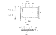
- . 2A is a top view of the capacitor body in the electrochemical capacitor shown in FIG. 1
- FIG. 2B is a front view of the capacitor body.
- 3A is a top view of the case component in the electrochemical capacitor shown in FIG. 1, and FIG. 3B is a right side view of the case component.
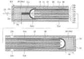
- FIG. 4 is an enlarged cross-sectional view taken along line S1-S1 of FIG.
- FIG. 5 is an enlarged cross-sectional view taken along line S2-S2 of FIG.
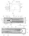
- FIG. 7A is a top view of an electrochemical capacitor showing a second embodiment of the present invention
- FIG. 7B is an enlarged sectional view taken along line S3-S3 in FIG. 7A
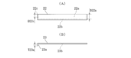
- 8A and 8B show a modification of the case component in the electric capacitor shown in FIGS. 1 and 7, and FIG. 8A is a right side view of one case component.
- 8 (B) is a right side view of the other case component.
- the electrochemical capacitor ECC shown in these drawings includes a capacitor main body 10, a case 20, and an inner portion 30.
- the capacitor body 10 is electrically connected to the film package 11, the chargeable / dischargeable power storage element 12 encapsulated in the film package 11 together with an electrolyte (no symbol), and the rear end portion of the power storage element 12 in the film package 11.
- a pair of terminals 13 connected to each other and having a front end portion led out of the film package 11 are provided.
- the film package 11 is made of a laminate film having at least a protective layer, a barrier layer, and a seal layer, and is formed in a rectangular shape.
- a rectangular laminate film of a predetermined size is folded in two so that the seal layers face each other, and heat is applied to the three outer edges (left side, right side, and front side) of the rectangular laminate film so that the seal layers are mutually attached. It is formed by fusing. That is, heat is applied to the left and right and front edges of the rectangular laminate film in a state where the film is folded in two so that the seal layers face each other.
- strip-shaped seal portions 11a to 11c are formed on the left side, the right side, and the front side of the outer edge of the film package 11 (that is, the left and right and front edges of the film package 11), respectively.
- the seal part 11c is formed so as to be continuous with the seal part 11a and the seal part 11b.
- the front-rear dimension L11 of the film package 11 is slightly smaller than the front-rear dimension L21a of the storage recess 21a of the case component 21, which will be described later, and the left-right dimension W11 is slightly smaller than the left-right dimension W21a of the storage recess 21a.
- T11 is slightly smaller than the double value of the vertical dimension D21a of the storage recess 21a.
- the laminate film for the film package 11 is a three-layer laminate film having a protective layer, a barrier layer, and a seal layer in this order.
- the protective layer is made of a thermoplastic such as nylon or polyethylene phthalate and has a thickness of 10 to 50 ⁇ m.
- the barrier layer is made of a metal such as aluminum or a metal oxide and has a thickness of 10 to 50 ⁇ m.
- the seal layer is made of a thermoplastic plastic such as polypropylene or modified polypropylene, and has a thickness of 30 to 50 ⁇ m.
- the storage element 12 is formed by laminating a collector electrode layer, a polarizable electrode layer, and a separate film in a predetermined order.
- the storage element 12 includes, in order from top to bottom, a collector electrode layer 12a, a polarizable electrode layer 12b, a separate film 12c, a polarizable electrode layer 12d, a collector electrode layer 12e, and a polarizability.
- the electrode layer 12f, the separate film 12g, the polarizable electrode layer 12h, and the collector electrode layer 12i are formed by laminating adjacent layers so that they are in close contact with each other.
- a rectangular terminal connection portion 12e1 is integrally formed on the right side of the front edge of the collector electrode layer 12e in the center in the stacking direction, and a rectangular terminal connection portion ( Are formed integrally.
- the electricity storage element 12 is enclosed with an electrolyte (not shown) in the film package 11 so that each terminal connection portion faces the front side.
- the collector electrode layers 12a, 12e, and 12i are made of a conductive material such as aluminum or platinum, and the thickness thereof is 5 to 50 ⁇ m.
- the polarizable electrode layers 12b, 12d, 12f and 12h are made of an active material such as PAS (polyacenic organic semiconductor) or activated carbon, and have a thickness of 10 to 50 ⁇ m.
- the seperate films 12c and 12g are made of an ion permeable film such as a cellulose film or a plastic film, and the thickness thereof is 10 to 50 ⁇ m.
- Each terminal 13 has a strip shape having a front-rear dimension (no symbol) larger than the left-right dimension W13.
- the rear end portion of one terminal 13 is electrically connected to the terminal connection portion 12e1 of the collector electrode layer 12e of the power storage element 12 by a technique such as spot welding, and the rear end portion of the other terminal 13 is the collector electrode layer.
- the terminals 12a and 12i are electrically connected by the same method.
- the front end portions of both terminals 13 are led out of the film package 11 through the front seal portion 11c of the film package 11 in a direction parallel to each other. *
- the terminal 13 is made of a conductive material such as aluminum or platinum and has a thickness of 50 to 100 ⁇ m. Further, a metal film such as tin or gold is formed on the tip of each terminal 13 by plating.
- a preferred method for manufacturing the capacitor body 10 shown in FIG. 2 will be described.
- a rectangular laminate film of a predetermined size is disposed so that the seal layer faces upward, and the storage element 12 with the terminals 13 is placed on the seal layer with both terminals 13 extending in the front-rear direction of the rectangular laminate film. It arrange
- the rectangular laminate film is folded in half at the center in the front-rear direction so that the seal layer is opposed, and heat is applied to the left and right sides of the outer edge (that is, the left and right edges of the rectangular laminate film) using an appropriate heating device.
- the left seal portion 11a and the right seal portion 11b are formed by fusing the seal layers together.
- a bag-shaped film package in which the front seal portion 11c is not formed is created.
- an electrolyte is injected into the bag-shaped film package through the front opening of the bag-shaped film package, and heat is applied to the front side of the outer edge (that is, the front edge of the rectangular laminated film) using the same heating device. And the seal layers are fused together to form the front seal portion 11c.
- This electrolyte is, for example, a liquid obtained by adding triethylmethylammonium borofluoride to propylene carbonate as a solvent, or a gel obtained by further adding polyacrylonitrile or the like to this liquid electrolyte.
- both terminals 13 are disposed between the upper and lower sealing layers constituting the front seal portion 11c, and the front end portions of both terminals 13 are led out of the film package 11.
- the left seal portion 11a and the right seal portion 11b are formed by bending a flat portion obtained by fusing the seal layers together into a U shape, and applying heat again to the bent portion. It is formed into a form. Thereby, sealing performance improves.
- the front seal portion 11c is not bent like the left seal portion 11a or the right seal portion 11b.
- the auxiliary seal layer improves the sealing performance of the front seal portion 11c. be able to. According to such an auxiliary seal layer, it is possible to improve the sealability of the portion where both terminals 13 are present, and therefore it is possible to avoid the problem that both terminals 13 come into contact with the barrier layer due to the melt flow of the seal layer. .
- the case 20 is formed by combining two case components 21 shown in FIG. 1, FIG. 3, FIG. 4 and FIG.
- the case 20 is formed by combining two case components 21 shown in FIG.
- the case component 21 has an integrally formed rectangular bottom wall, front and rear left and right walls, and a housing recess 21a having a rectangular shape when viewed from above.
- the front-rear dimension L21a of the storage recess 21a is slightly larger than the front-rear dimension L11 of the film package 11 of the capacitor body 10
- the left-right dimension W21a is slightly larger than the left-right dimension W11 of the film package 11
- the vertical dimension D21a is slightly larger than a half value of the vertical dimension T11 of the film package 11.
- one vent hole 21b penetrating through the bottom wall is formed at a substantially central position of the bottom wall of the case component 21 (the bottom wall of the housing recess 21a).
- a left-right dimension W21c slightly larger than the left-right dimension W13 of each terminal 13 of the capacitor body 10 and a vertical dimension D21c corresponding to 1/2 of the thickness of the terminal 13 are provided on the upper surface of the front wall of the case component 21, a left-right dimension W21c slightly larger than the left-right dimension W13 of each terminal 13 of the capacitor body 10 and a vertical dimension D21c corresponding to 1/2 of the thickness of the terminal 13 are provided.
- the two rectangular cutouts 21c having a length are formed so as to be separated from each other by a length corresponding to the distance between the terminals 13.
- the case component 21 is made of thermosetting plastic such as polyimide, epoxy resin, or glass fiber or the like that has been improved in strength (FRP).
- the thickness of the left and right walls is 100 to 300 ⁇ m.
- the case 20 shown in FIGS. 4 and 5 has two case components 21 prepared so that the openings are aligned with each other and the rectangular cutouts 21c are matched with each other. It is formed by combining the component parts 21. Since the combined two case components 21 are joined by an inner portion 30 which will be described in detail later, the case 20 has a rectangular parallelepiped shape in which the longitudinal dimension is L21a, the lateral dimension is W21a, and the vertical dimension is twice the value of D21a. Storage space SR is formed. Further, two lead-out holes (no symbol) for the terminal 13 are formed in the front wall of the case 20 by a rectangular cutout 21c that matches the vertical direction.
- the storage space SR of the case 20 stores the bases of the lead portions of the film body 11 and both terminals 13 of the capacitor body 10, and the leading ends of the lead portions of both terminals 13 are rectangular. It is exposed outside the case 20 through two lead-out holes formed by the notches 21c.
- the front-rear dimension (L21a) of the storage space SR of the case 20 is slightly larger than the front-rear dimension L12 of the film package 1, and the left-right dimension (W21a) is slightly smaller than the left-right dimension W12 of the film package 11.
- the vertical dimension (double value of D21a) is slightly larger than the vertical dimension T12 of the film package 11.
- a gap Ga is formed between the rear edge of the film package 11 and the inner surface of the rear wall of the case 20, and a gap Gb is formed between the rear edge of the film package 11 and the inner surface of the rear wall of the case 20.
- a gap Gc is formed between the left edge (the left edge of the left seal portion 11a) and the inner surface of the left wall of the case 20, and the right edge of the film package 11 (the left edge of the right seal portion 11b) and the case 20
- a gap Gd is formed between the inner surface of the right wall.
- a clearance CLu is formed between the upper surface of the film package 11 and the inner surface of the upper wall of the case 20, and a clearance CLd is formed between the lower surface of the film package 11 and the inner surface of the bottom wall of the case 20.
- the regions where the inner portions 30 on the upper and lower surfaces of the film package 11 stored in the storage space SR do not exist are not in contact with the inner surface of the case 20.
- vent 21 b on the upper wall of the case 20 faces a region where the inner portion 30 on the upper surface of the film package 11 does not exist via a clearance CLu
- the vent 21 b on the lower wall of the case 20 is an inner surface on the lower surface of the film package 11. It faces the region where the portion 30 does not exist via the clearance CLd.
- the clearances CLu and CLd formed in the storage space SR communicate with the outside air through the vent holes 21b.
- the inner part 30 joins the upper and lower case component parts 21 combined to fix the film package 11 of the capacitor body 10 in the storage space SR of the case 20.
- the inner portion 30 is made of a thermosetting plastic such as polyimide, epoxy resin, or glass fiber or the like that has been improved in strength (FRP).
- FRP in strength
- the inner portion 30 is provided in a rectangular frame shape in a region corresponding to the rear edge of the film package 11 and the three seal portions 11a to 11c in the storage space SR of the case 20.
- the portion of the inner portion 30 existing on the front side of the film package 11 is in close contact with the bottom wall inner surface and front wall inner surface of the lower case component 21 and the upper wall inner surface and front wall inner surface of the upper case component 21.
- the front side seal portion 11c of the film package 11, the inner side of the front side seal portion 11c, and the roots of the lead-out portions of the terminals 13 are covered.
- the portion of the inner portion 30 existing on the rear side of the film package 11 is in close contact with the bottom wall inner surface and the rear wall inner surface of the lower case component 21 and the upper wall inner surface and the rear wall inner surface of the upper case component 21.
- the rear portion of the film package 11 is covered.
- the portion existing on the left side of the film package 11 of the inner portion 30 is in close contact with the bottom wall inner surface and the left wall inner surface of the lower case component 21 and the upper wall inner surface and the left wall inner surface of the upper case component 21, The left seal part 11a of the film package 11 and the inner part of the left seal part 11c are covered. Furthermore, the portion existing on the right side of the film package 11 of the inner portion 30 is in close contact with the bottom wall inner surface and the right wall inner surface of the lower case component 21 and the upper wall inner surface and the right wall inner surface of the upper case component 21, The right seal part 11b of the film package 11 and the inner part of the right seal part 11b are covered. That is, the upper and lower two case components 21 constituting the case 20 are coupled by the inner portion 30, and the film package 11 of the capacitor body 10 accommodated in the accommodation space SR of the case 20 is accommodated by the inner portion 30. Fixed in SR.
- the preferable manufacturing method of the electrochemical capacitor ECC shown in FIG. 1 will be described.
- the capacitor main body 10 shown in FIG. 2 and the case component 21 shown in FIG. 3 are prepared in advance.
- the fluid inner portion M30 is applied around the housing recess 21a of the lower case component 21 using an appropriate applicator.
- the flowable inner part M30 after application is pressed down by the film package 11 of the capacitor body 10 and expands toward the vent 21b (see the two-dot chain line in FIG. 6A). Adjust in advance.
- the film package 11 of the capacitor body 10 is inserted from above into the storage recess 21a coated with the fluid inner portion M30, and both the terminals 13 are rectangular cutouts 21c, Each is inserted into 21c.
- the film package 11 of the capacitor main body 10 is inserted into the storage recess 21a from above, the film package is provided at substantially the center of the storage recess 21a so that the gaps Ga, Gb, Gc and Gd shown in FIGS. 11 is arranged.
- the fluid inner portion M30 is applied around the storage recess 21a of the upper case component 21, and the storage recess
- the upper case configuration is such that the opening of 21a is aligned with the opening of the housing recess 21a of the lower case component 21 and the rectangular notch 21c matches the rectangular notch 21c of the lower case component 21.
- the component 21 is combined with the lower case component 21 in an overlapping manner.
- the upper and lower case components 21 and 21 combined with each other are allowed to stand for a predetermined time in a temperature atmosphere in which the fluid inner part M30 can be cured to cure the fluid inner part M30.
- the fluid inner part M30 is an epoxy resin
- the case components 21 and 21 are allowed to stand in a temperature atmosphere of 100 to 150 degrees.
- the flowable inner portion M30 protrudes from the boundary between the two case components 21, so that the flowable inner portion M30 is It is desirable to remove the protruding portion before curing or after curing the fluid inner portion M30.
- both terminals 13 of the electrochemical capacitor ECC bent as necessary are connected to the circuit board via cream solder in the same manner as other electronic components.
- the circuit board on which the electrochemical capacitor ECC is arranged is placed in a reflow furnace.
- the film package 11 of the capacitor body 10 is stored in the storage space SR of the case 20, the main heating time in the temperature profile of reflow soldering is used.
- the heat conduction to the film package 11 is delayed by the case 20 as compared with the case without the case 20, so that the internal pressure of the film package 11 increases due to an increase in the vapor pressure of the electrolyte, etc.
- Softening of the sealing material 11c can be suppressed.
- the case 20 is formed of polyimide or thermosetting plastic, the suppression can be more effectively performed by the heat resistance of the case 20 itself.
- the temperature of the film package 11 rises to a temperature close to the peak temperature (for example, 260 to 280 ° C.), thereby increasing the vapor pressure of the electrolyte.
- the sealing material of each of the seal portions 11a to 11c may be softened.
- the seal portions 11a to 11c of the film package 11 of the capacitor body 10 housed in the housing space SR of the case 20 are covered with the inner portion 30.
- the seal reinforcement is made, even if the internal pressure of the film package 11 rises or the sealing material of each of the seal portions 11a to 11c softens, the electrolyte, gas, etc. in the film package 11 Leakage from each of the seal portions 11a to 11c can be suppressed by the covering.
- the inner part 30 is formed from polyimide or a thermosetting plastic, it is possible to more effectively suppress leakage of electrolyte, gas, and the like due to the heat resistance and rigidity of the inner part 30 itself. .
- a gap Ga is formed between the front edge of the film package 11 (front edge of the front seal portion 11c) and the inner surface of the front wall of the case 20, and the left edge of the film package 11 (left side of the left seal portion 11a) is formed.
- a gap Gc is formed between the right edge of the film package 11 and the inner surface of the right wall of the case 20. Since a sufficient amount of the inner portion 30 is disposed in the gaps Ga, Gc and Gd and each of the seal portions 11a to 11c can be firmly covered, electrolyte, gas, etc. leak out. Can be more effectively suppressed. Furthermore, since not only each seal part 11a-11c but the inner part is coat
- the film package 11 is stored in the storage space SR of the case 20
- the outermost layer of the film package 11 is made of a water-holding material such as nylon
- water vapor generated from the outermost layer is used.
- the internal pressure of the storage space SR of the case 20 is increased, and a force in the direction of crushing the film package 11 and the storage element 12 can be applied.
- the vent 21b on the upper wall of the case 20 faces the region where the inner portion 30 on the upper surface of the film package 11 does not exist via the clearance CLu
- the vent 21b on the lower wall of the case 20 faces a region where the inner portion 30 on the lower surface of the film package 11 does not exist via the clearance CLd
- the water vapor is generated even if water vapor is generated from the outermost layer of the film package 11.
- the air can be smoothly released to the outside air, and an increase in the internal pressure of the storage space SR can be suppressed.
- the electrochemical capacitor ECC according to one embodiment of the present invention, it can be mounted on a circuit board by reflow soldering similar to other electronic components without causing the conventional problems. . Thereby, productivity can be improved and production cost can be greatly reduced with respect to mounting of the electrochemical capacitor ECC.
- FIG. 7 shows a second embodiment of the present invention.
- the electrochemical capacitor ECC shown in the figure is different from that of the first embodiment in that the inner portion 30 ′ is a U-shaped region corresponding to the three seal portions 11 a to 11 c of the film package 11 in the storage space SR of the case 20. It is in the point provided in the shape.
- the portion of the inner portion 30 ′ existing on the front side of the film package 11 is in close contact with the bottom wall inner surface and front wall inner surface of the lower case component 21 and the upper wall inner surface and front wall inner surface of the upper case component 21, and the film
- the seal part 11c on the front side of the package 11, the inner part of the seal part 11c on the front side, and the root of the lead-out part of both terminals 13 are covered.
- the portion of the inner portion 30 ′ on the left side of the film package 11 is in close contact with the bottom wall inner surface and the left wall inner surface of the lower case component 21 and the upper wall inner surface and the left wall inner surface of the upper case component 21.
- the left seal part 11a of the film package 11 and the inner part of the left seal part 11c are covered.
- the portion of the inner part 30 ′ on the right side of the film package 11 is in close contact with the bottom wall inner surface and the right wall inner surface of the lower case component 21 and the upper wall inner surface and the right wall inner surface of the upper case component 21.
- the right seal part 11b of the film package 11 and the inner part of the right seal part 11b are covered.
- clearances CLb communicating with the upper and lower clearances CLu and CLd are formed on the rear side of the film package 11.
- the two upper and lower case component parts 21 are combined and the film package 11 of the capacitor body 10 is placed in the storage space SR of the case 20, as in the first embodiment. Can be fixed. Further, the behavior of the electrochemical capacitor ECC and the effect based on the behavior when the electrochemical capacitor ECC shown in FIG. 7A is mounted on a circuit board by reflow soldering in the same manner as other electronic components are the first embodiment. The same as described in the form.
- the gaps Ga, Gb, Gc, and Gd have the same dimensions. However, if the gap dimension is larger than zero, the gaps Ga, Gb, Gc The same effect as described above can be obtained even if the dimensions of Gd and Gd are not necessarily the same.
- the clearances CLu and CLd having the same dimension are shown.
- the clearance dimension is larger than zero, the clearances CLu and CLd are not necessarily the same dimension.
- the same effect as described above can be obtained.
- the upper surface of the film package 11 is not fixed to the inner surface of the upper wall of the case 20, and the lower surface of the film package 11 is attached to the inner surface of the bottom wall of the case 20. If it is not fixed, it is sufficiently possible to smoothly release water vapor or the like to the outside air through the upper and lower vents 21b.
- the case component 21 for the case 20 is provided with one vent 21b, but the number of vents 21b may be two or more. The same effect as described above can be obtained. However, if the number of vents 21b is increased, the amount of heat penetration from the outside increases. Therefore, when the number of vents 21b is two or more, it is desirable to make the hole diameter smaller than one.
- the case 20 is configured by combining the two case components 21 shown in FIG. 3, but FIG. 8 (A) and FIG. 8 (B). ), The case 20 may be configured by combining two case components 22 and 23 having different shapes.
- one case component 22 is formed in a box shape having a rectangular bottom wall, front wall, rear wall, left wall, and right wall.
- the case component 22 has a storage recess 22a having a rectangular shape when viewed from above and having an open top surface.
- the front-rear dimension of the storage recess 22a is the same as the front-rear dimension L21a shown in FIG. 3, the left-right dimension is the same as the left-right dimension W21a shown in FIG. 3, and the vertical dimension D21a is equal to the vertical dimension D21a shown in FIG. 2 times.
- the left and right dimensions of the two rectangular cutouts 22c are the same as the left and right dimension W13 shown in FIG. 3, and the vertical dimension D22c is equal to the sum of the vertical dimension D21c and the vertical dimension D21a shown in FIG.
- the other case component 23 corresponds to a case in which the front wall, the rear wall, the left wall, and the right wall are removed from the case component 21 shown in FIG. 3, and is formed in a rectangular shape in a top view.
- a rectangular insertion piece 23a, 23a having the same vertical dimension as the vertical dimension D21a shown in FIG. 3 is integrally formed on the lower surface of the front edge of the case component 23, which can be inserted into the two rectangular cutouts 22c, 22c.
- One vent hole 22b is formed at the approximate center position of the bottom wall of the case component 22 (the bottom wall of the storage recess 22a), and one vent hole 23b is formed at the approximate center position of the case component 23. .
- the number of each vent 22b and 23b may be two or more.
- a rectangular laminate film of a predetermined size is folded in two so that the seal layer faces each other, and heat is applied to the outer edge on the three sides (left side, right side, and front side).
- the film package 11 according to another embodiment of the present invention is formed by laminating two rectangular laminate films of a predetermined size so that the seal layers face each other. Further, it may be formed by applying heat to the four sides (left side, right side, front side, and rear side) of the outer edge and fusing the seal layers together.
- the film package formed in this way has a strip-shaped seal portion formed continuously on the left side and the right side of the outer edge and on the rear side of the front side, the inner portion 30 is disposed as in the first embodiment.
- an electrochemical capacitor having the same effect as the electrochemical capacitor ECC according to the first embodiment can be obtained.
- the present invention can be widely applied to various electrochemical capacitors such as electric double layer capacitors, lithium ion capacitors and redox capacitors.
- ECC electrochemical capacitor, 10 ... capacitor body, 11 ... film package, 11a, 11b, 11c ... sealing part, 12 ... electric storage element, 13 ... terminal, 20 ... case, 21, 22, 23 ... case components, 21b, 22b, 23b ... vent, SR ... storage space, 30, 30 '... inner part, Ga, Gb, Gc, Gd ... gap, Clu, CLd, CLb ... clearance.
Landscapes
- Engineering & Computer Science (AREA)
- Power Engineering (AREA)
- Microelectronics & Electronic Packaging (AREA)
- Electric Double-Layer Capacitors Or The Like (AREA)
Abstract
Description
前記ケースの内壁の少なくとも一部分と前記パッケージの接合箇所との間に介在して前記パッケージを支持するとともに、前記パッケージの接合箇所を被覆する熱硬化性のインナー部材と、を備える。
図1~図6は本発明の第1実施形態を示す。これらの図に示した電気化学キャパシタECCは、キャパシタ本体10と、ケース20と、インナー部30と、を具備している。
されている。この蓄電素子12は、詳しくは、上から下に向かって順に、集電極層12aと、分極性電極層12bと、セパレートフィルム12cと、分極性電極層12dと、集電極層12eと、分極性電極層12fと、セパレートフィルム12gと、分極性電極層12hと、集電極層12iと、を隣接する層同士を互いに密着するように積層することによって形成される。積層方向中央の集電極層12eの前縁右側には矩形状の端子接続部12e1が一体に形成され、積層方向上下の集電極層12a及び12iの前縁左側には矩形状の端子接続部(符号無し)が一体に形成されている。この蓄電素子12は、各端子接続部が前側を向くように、前記フィルムパッケージ11内に電解質(図示省略)と共に封入されている。
図7は本発明の第2実施形態を示す。同図に示した電気化学キャパシタECCが第1実施形態と異なるところは、インナー部30’がケース20の収納空間SR内におけるフィルムパッケージ11の3つのシール部11a~11cに対応する領域にコ字状に設けられている点にある。
(1)第1実施形態及び第2実施形態では、各ギャップGa,Gb,Gc及びGdの寸法を全て同じくしたものを示したが、ギャップ寸法が零よりも大きければ各ギャップGa,Gb,Gc及びGdの寸法は必ずしも同じでなくても前記同様の効果を得ることができる。
Claims (6)
- 表面の少なくとも縁部に熱可塑性のシール部材を備える一組のシートからなり、当該一組のシートが前記シール部材で接合されてなるパッケージと、
前記パッケージに収容される蓄電素子及び電解質と、
前記パッケージを収容するケースと、
前記パッケージの接合箇所と前記ケースの内壁の少なくとも一部分との間に介在して前記パッケージを支持するとともに、前記パッケージの接合箇所を被覆するインナー部材と、
を備える電気化学キャパシタ。 - 前記一組のシートが、折り曲げられた1枚のシートからなる請求項1に記載の電気化学キャパシタ。
- 前記一組のシートが、2枚のシートからなる請求項1に記載の電気化学キャパシタ。
- 前記パッケージが、前記インナー部材によって前記ケースと直接接触しないように支持される請求項1に記載の電気化学キャパシタ。
- 前記ケースの内壁、前記パッケージ、及び前記インナー部材によって規定される前記ケースの内部の空間と、前記ケースの外部とを連絡する連絡孔が前記ケースに少なくとも1つ形成された請求項1に記載の電気化学キャパシタ。
- 前記電子部品が、蓄電素子及び電解質を有するキャパシタである請求項1に記載の電気化学キャパシタ。
Priority Applications (3)
| Application Number | Priority Date | Filing Date | Title |
|---|---|---|---|
| CN201080054441.XA CN102640243B (zh) | 2009-10-05 | 2010-08-31 | 电化学电容器 |
| US13/500,272 US8902594B2 (en) | 2009-10-05 | 2010-08-31 | Electrochemical capacitor |
| JP2011535315A JP5427239B2 (ja) | 2009-10-05 | 2010-08-31 | 電気化学キャパシタ |
Applications Claiming Priority (2)
| Application Number | Priority Date | Filing Date | Title |
|---|---|---|---|
| JP2009231585 | 2009-10-05 | ||
| JP2009-231585 | 2009-10-05 |
Publications (1)
| Publication Number | Publication Date |
|---|---|
| WO2011043138A1 true WO2011043138A1 (ja) | 2011-04-14 |
Family
ID=43856618
Family Applications (1)
| Application Number | Title | Priority Date | Filing Date |
|---|---|---|---|
| PCT/JP2010/064768 Ceased WO2011043138A1 (ja) | 2009-10-05 | 2010-08-31 | 電気化学キャパシタ |
Country Status (4)
| Country | Link |
|---|---|
| US (1) | US8902594B2 (ja) |
| JP (1) | JP5427239B2 (ja) |
| CN (1) | CN102640243B (ja) |
| WO (1) | WO2011043138A1 (ja) |
Cited By (2)
| Publication number | Priority date | Publication date | Assignee | Title |
|---|---|---|---|---|
| JP2019062082A (ja) * | 2017-09-27 | 2019-04-18 | 太陽誘電株式会社 | 蓄電モジュール |
| JP2021174579A (ja) * | 2020-04-20 | 2021-11-01 | 日本特殊陶業株式会社 | 電池 |
Families Citing this family (9)
| Publication number | Priority date | Publication date | Assignee | Title |
|---|---|---|---|---|
| JPWO2013094423A1 (ja) * | 2011-12-22 | 2015-04-27 | 株式会社村田製作所 | 蓄電デバイス |
| DE102013003559B4 (de) * | 2013-03-01 | 2014-12-11 | Compur Monitors Gmbh & Co. Kg | Verfahren zur Erzeugung von Blausäuregas in einer elektrochemischen Zelle |
| JP6424827B2 (ja) | 2013-10-17 | 2018-11-21 | ソニー株式会社 | 光源装置、光源ユニット、及び画像表示装置 |
| MY195773A (en) | 2016-05-20 | 2023-02-11 | Kyocera Avx Components Corp | Multi-Cell Ultracapacitor |
| US11830672B2 (en) | 2016-11-23 | 2023-11-28 | KYOCERA AVX Components Corporation | Ultracapacitor for use in a solder reflow process |
| CN111600057B (zh) * | 2020-05-15 | 2021-10-29 | 郑州仿弦新材料科技有限公司 | 一种具有曲面结构的复合材料结构电池及其制备方法与应用 |
| CN111600056B (zh) * | 2020-05-15 | 2021-10-29 | 郑州仿弦新材料科技有限公司 | 一种储能复合材料结构电池的制备方法 |
| CN111863459B (zh) * | 2020-06-28 | 2021-10-08 | 华中科技大学 | 一种贴片式微型滤波电容器的制备方法与应用 |
| WO2022133419A1 (en) * | 2020-12-15 | 2022-06-23 | Emerson Professional Tools, Llc | Power tool with hybrid supercapacitors |
Citations (4)
| Publication number | Priority date | Publication date | Assignee | Title |
|---|---|---|---|---|
| JPH10112297A (ja) * | 1996-10-08 | 1998-04-28 | Shin Kobe Electric Mach Co Ltd | 蓄電池保護ケース及びその使用方法 |
| JP2009016549A (ja) * | 2007-07-04 | 2009-01-22 | Nissin Electric Co Ltd | 電気二重層コンデンサ |
| JP2009188195A (ja) * | 2008-02-06 | 2009-08-20 | Taiyo Yuden Co Ltd | 電気化学デバイス及びその実装構造 |
| JP2009212081A (ja) * | 2008-02-04 | 2009-09-17 | Panasonic Corp | 電池パック、それを備えた電子機器および電池収納部を備えた電子機器 |
Family Cites Families (7)
| Publication number | Priority date | Publication date | Assignee | Title |
|---|---|---|---|---|
| JP3136903B2 (ja) * | 1994-06-09 | 2001-02-19 | 松下電器産業株式会社 | 熱電池 |
| JP2000223085A (ja) | 1999-01-28 | 2000-08-11 | Mitsubishi Chemicals Corp | 二次電池 |
| JP2000286171A (ja) * | 1999-03-30 | 2000-10-13 | Tokin Ceramics Corp | 電気二重層コンデンサ |
| IL155790A0 (en) * | 2000-11-09 | 2003-12-23 | Foc Frankenburg Oil Company Es | A supercapacitor and a method of manufacturing such a supercapacitor |
| JP2003133184A (ja) * | 2001-10-22 | 2003-05-09 | Sony Corp | シート型コンデンサ |
| JP5319129B2 (ja) | 2008-02-01 | 2013-10-16 | 太陽誘電株式会社 | 電気化学デバイス |
| WO2009136660A1 (ja) * | 2008-05-08 | 2009-11-12 | 太陽誘電株式会社 | 電気化学デバイスおよびその実装構造 |
-
2010
- 2010-08-31 US US13/500,272 patent/US8902594B2/en not_active Expired - Fee Related
- 2010-08-31 WO PCT/JP2010/064768 patent/WO2011043138A1/ja not_active Ceased
- 2010-08-31 CN CN201080054441.XA patent/CN102640243B/zh not_active Expired - Fee Related
- 2010-08-31 JP JP2011535315A patent/JP5427239B2/ja not_active Expired - Fee Related
Patent Citations (4)
| Publication number | Priority date | Publication date | Assignee | Title |
|---|---|---|---|---|
| JPH10112297A (ja) * | 1996-10-08 | 1998-04-28 | Shin Kobe Electric Mach Co Ltd | 蓄電池保護ケース及びその使用方法 |
| JP2009016549A (ja) * | 2007-07-04 | 2009-01-22 | Nissin Electric Co Ltd | 電気二重層コンデンサ |
| JP2009212081A (ja) * | 2008-02-04 | 2009-09-17 | Panasonic Corp | 電池パック、それを備えた電子機器および電池収納部を備えた電子機器 |
| JP2009188195A (ja) * | 2008-02-06 | 2009-08-20 | Taiyo Yuden Co Ltd | 電気化学デバイス及びその実装構造 |
Cited By (3)
| Publication number | Priority date | Publication date | Assignee | Title |
|---|---|---|---|---|
| JP2019062082A (ja) * | 2017-09-27 | 2019-04-18 | 太陽誘電株式会社 | 蓄電モジュール |
| JP2021174579A (ja) * | 2020-04-20 | 2021-11-01 | 日本特殊陶業株式会社 | 電池 |
| JP7473383B2 (ja) | 2020-04-20 | 2024-04-23 | 日本特殊陶業株式会社 | 電池 |
Also Published As
| Publication number | Publication date |
|---|---|
| JP5427239B2 (ja) | 2014-02-26 |
| JPWO2011043138A1 (ja) | 2013-03-04 |
| US20120257357A1 (en) | 2012-10-11 |
| US8902594B2 (en) | 2014-12-02 |
| CN102640243B (zh) | 2015-06-03 |
| CN102640243A (zh) | 2012-08-15 |
Similar Documents
| Publication | Publication Date | Title |
|---|---|---|
| JP5427239B2 (ja) | 電気化学キャパシタ | |
| KR101146343B1 (ko) | 전기화학 디바이스 | |
| JP7217404B2 (ja) | コンデンサ | |
| JP5835433B2 (ja) | フィルム外装電気デバイス | |
| JP2009224147A (ja) | フィルム外装電気デバイス及び組電池 | |
| JP6004112B2 (ja) | ラミネート型蓄電デバイスの製造方法 | |
| US9023510B2 (en) | Electrochemical device | |
| JP5725113B2 (ja) | 組電池およびフィルム外装電気デバイス | |
| JP2006164784A (ja) | フィルム外装電気デバイス | |
| JP5349345B2 (ja) | 電気化学デバイス | |
| US20190157632A1 (en) | Battery | |
| JP2005019213A (ja) | 電気リード部の構造、該リード部構造を有する電気デバイス、電池および組電池 | |
| CN109564990B (zh) | 电化学装置 | |
| JP2009064946A (ja) | 電気二重層キャパシタ | |
| JP2020017401A (ja) | 蓄電装置及び蓄電装置の製造方法 | |
| CN101329945B (zh) | 引脚外接式电解电容器 | |
| JP2007273606A (ja) | ラミネートフィルム外装電子部品 | |
| JP2009188195A (ja) | 電気化学デバイス及びその実装構造 | |
| JP5347389B2 (ja) | 蓄電デバイス | |
| JP5011499B2 (ja) | 電子部品 | |
| JP4710049B2 (ja) | 電子部品及びその製造方法 | |
| JP2013197267A (ja) | コンデンサ | |
| KR20160051060A (ko) | 파우치형 이차전지 및 이에 적용되는 전극 리드 어셈블리 | |
| JP5590161B2 (ja) | フィルム外装電気デバイス及び組電池 | |
| CN117321850A (zh) | 接合方法以及蓄电器件 |
Legal Events
| Date | Code | Title | Description |
|---|---|---|---|
| WWE | Wipo information: entry into national phase |
Ref document number: 201080054441.X Country of ref document: CN |
|
| 121 | Ep: the epo has been informed by wipo that ep was designated in this application |
Ref document number: 10821809 Country of ref document: EP Kind code of ref document: A1 |
|
| WWE | Wipo information: entry into national phase |
Ref document number: 2011535315 Country of ref document: JP |
|
| NENP | Non-entry into the national phase |
Ref country code: DE |
|
| WWE | Wipo information: entry into national phase |
Ref document number: 13500272 Country of ref document: US |
|
| 122 | Ep: pct application non-entry in european phase |
Ref document number: 10821809 Country of ref document: EP Kind code of ref document: A1 |