WO2011027537A1 - Scintillator material - Google Patents
Scintillator material Download PDFInfo
- Publication number
- WO2011027537A1 WO2011027537A1 PCT/JP2010/005345 JP2010005345W WO2011027537A1 WO 2011027537 A1 WO2011027537 A1 WO 2011027537A1 JP 2010005345 W JP2010005345 W JP 2010005345W WO 2011027537 A1 WO2011027537 A1 WO 2011027537A1
- Authority
- WO
- WIPO (PCT)
- Prior art keywords
- csi
- emission
- composition
- emission peak
- wavelength
- Prior art date
- Legal status (The legal status is an assumption and is not a legal conclusion. Google has not performed a legal analysis and makes no representation as to the accuracy of the status listed.)
- Ceased
Links
Images


Classifications
-
- C—CHEMISTRY; METALLURGY
- C09—DYES; PAINTS; POLISHES; NATURAL RESINS; ADHESIVES; COMPOSITIONS NOT OTHERWISE PROVIDED FOR; APPLICATIONS OF MATERIALS NOT OTHERWISE PROVIDED FOR
- C09K—MATERIALS FOR MISCELLANEOUS APPLICATIONS, NOT PROVIDED FOR ELSEWHERE
- C09K11/00—Luminescent, e.g. electroluminescent, chemiluminescent materials
- C09K11/08—Luminescent, e.g. electroluminescent, chemiluminescent materials containing inorganic luminescent materials
- C09K11/62—Luminescent, e.g. electroluminescent, chemiluminescent materials containing inorganic luminescent materials containing gallium, indium or thallium
- C09K11/626—Halogenides
- C09K11/628—Halogenides with alkali or alkaline earth metals
Definitions
- the present invention relates to a scintillator material.
- the present invention relates to a scintillator material that converts radiation into visible light.
- a known image detector for radiation diagnosis is a radiation detector that detects radiated X-rays to acquire an X-ray image as digital signals.
- Such radiation detectors are broadly divided into direct X-ray detectors and indirect X-ray detectors.
- the indirect X-ray detectors are detectors in which X-rays are changed into visible light with a phosphor, and the visible light is converted into charge signals with a photoelectric conversion element such as an amorphous silicon (a-Si) photodiode or a charge coupled device (CCD) to acquire an image.
- a-Si amorphous silicon
- CCD charge coupled device
- amorphous silicon a-Si
- a-Si amorphous silicon
- CsI:Tl cesium iodide:thallium
- CsI cesium iodide:thallium
- the emission peak wavelength of CsI:Tl varies in the wavelength band of about 540 to 565 nm depending on the concentration of thallium (Tl) added.
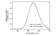
- Fig. 5A shows a change in the emission spectrum of a CsI:Tl scintillator material when the concentration of thallium (Tl) added was changed.
- Tl is added to CsI in a low concentration (0.010 mole percent)
- the scintillator material exhibits an emission peak at about 540 nm.
- the scintillator material when Tl is added to CsI in a high concentration (1.0 mole percent), the scintillator material exhibits an emission peak at about 565 nm (refer to Fig. 5A).
- the emission wavelength of CsI:Tl can be shifted to the long-wavelength side by adding Tl, which functions as a luminescence center, in a high concentration, whereby the emission wavelength can be made to coincide with the photosensitivity of a-Si.
- CsI:In A scintillator material (CsI:In) formed by adding indium (In) as a luminescence center to cesium iodide (CsI) also functions as a scintillator similarly to CsI:Tl.
- CsI:In-based materials conducted by the inventors of the present invention, the following became clear: In the cases where indium (In) was added to cesium iodide (CsI) in a low concentration (0.010 mol%) and a high concentration (1.0 mol%), the emission spectrum did not change, and these materials exhibited certain light emission at a wavelength of about 544 nm (refer to Fig. 5B).
- Fig. 5B shows the change in the emission spectrum between the CsI:In scintillator materials when the concentration of indium (In) added was changed.
- the inventors of the present invention found the following new problem: Unlike in the case of CsI:Tl, the emission wavelength of CsI:In cannot be shifted to the long-wavelength side by the technique in which the concentration of the luminescence center added is increased. Accordingly, the light emission cannot be adjusted to a wavelength range where detection sensitivity of a-Si is high.
- the present invention provides a scintillator material containing a CsI:In-based material that exhibits light emission in a wavelength range where photosensitivity of a-Si is high.
- a scintillator material according to the present invention contains a compound represented by a general formula [Cs 1-z Rb z ][I 1-x-y Br x Cl y ]:In.
- x, y, and z satisfy any one of conditions (1), (2), and (3) below.
- a scintillator material containing a CsI:In-based scintillator material that exhibits light emission in a wavelength range where photosensitivity of a-Si is high can be provided.
- Fig. 1 is a graph showing the relationship between the amount of Cl or Br added and the emission peak wavelength in scintillator materials of Examples 1 and 2 of the present invention.
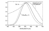
- Fig. 2 is a graph showing the relationship between the emission spectrum of a scintillator material of Example 1 of the present invention and sensor detection sensitivity.
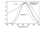
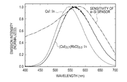
- Fig. 3 is a graph showing the relationship between the emission spectrum of a scintillator material of Example 2 of the present invention and sensor detection sensitivity.
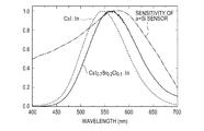
- Fig. 4 is a graph showing the relationship between the emission spectrum of a scintillator material of Example 3 of the present invention and sensor detection sensitivity.
- Fig. 5A is a graph showing a change in the emission spectrum between existing scintillator materials of CsI:Tl.
- Fig. 1 is a graph showing the relationship between the amount of Cl or Br added and the emission peak wavelength in scintillator materials of Examples 1 and 2 of the present invention.
- Fig. 2 is a graph showing the relationship between the emission spectrum of
- Fig. 5B is a graph showing a change in the emission spectrum between existing scintillator materials of CsI:In.
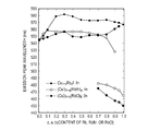
- Fig. 6 is a graph showing the relationship between the amount of Rb, RbBr, or RbCl added and the emission peak wavelength in scintillator materials of Examples 4, 5, and 6 of the present invention.
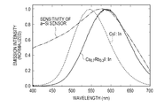
- Fig. 7 is a graph showing the relationship between the emission spectrum of a scintillator material of Example 4 of the present invention and sensor detection sensitivity.
- Fig. 8 is a graph showing the relationship between the emission spectrum of a scintillator material of Example 5 of the present invention and sensor detection sensitivity.
- Fig. 9 is a graph showing the relationship between the emission spectrum of a scintillator material of Example 6 of the present invention and sensor detection sensitivity.
- a feature of the present invention lies in that, in CsI:In, the emission wavelength is shifted to the long-wavelength side by replacing the I site of CsI, which is a parent material, with bromine (Br) or chlorine (Cl), which is a different halogen element, by replacing the Cs site of CsI with rubidium (Rb), which is a different alkali element, or by replacing both the I site and the Cs site with a different halogen element and a different alkali element, respectively, to obtain a scintillator material that exhibits light emission corresponding to a wavelength range where detection sensitivity of a-Si is high.
- wavelengths described below are not absolute values, and the values of the wavelength may vary depending on a measuring device or a calibration method. Therefore, in the present invention, a relative difference in wavelength between compositions is important, and the present invention does not specify absolute values of the wavelengths.
- a feature of a first embodiment lies in that, in CsI:In, the emission wavelength is shifted to the long-wavelength side by replacing the I site of CsI, which is a parent material, with Br or Cl, which is a different halogen element, to obtain a scintillator material that exhibits light emission corresponding to a wavelength range where detection sensitivity of a-Si is high.
- the scintillator material of this embodiment contains a compound represented by a general formula Cs[I 1-x-y Br x Cl y ]:In.
- the relationship 0 ⁇ x + y ⁇ 1 is satisfied, and at least one of Mathematical formula 4 and Mathematical formula 5 is satisfied.
- the content of indium (In) is 0.00010 mole percent or more and 1.0 mole percent or less relative to Cs[I 1-x-y Br x Cl y ].
- the scintillator material of this embodiment contains a compound represented by a general formula Cs[I 1-x-y Br x Cl y ]:In, in which the relationship 0 ⁇ x + y ⁇ 1 is satisfied, at least one of Mathematical formula 6 and Mathematical formula 7 is satisfied, and the content of indium (In) is 0.00010 mole percent or more and 1.0 mole percent or less relative to Cs[I 1-x-y Br x Cl y ].
- the composition of the parent material of the scintillator material is configured to contain a certain amount of CsCl or CsBr in addition to CsI, the scintillator material exhibits light emission at the long-wavelength side relative to light emission of CsI:In. The detail thereof will be described below.
- Fig. 1 is a graph showing the relationship between the amount of Cl or Br added and the emission peak wavelength in a scintillator material represented by CsI 1-x Br x :In or CsI 1-y Cl y :In.
- a composition range is present in which emission of yellow light having an emission peak at the longer-wavelength side with respect to 544 nm, which is the emission peak of CsI:In, occurs.
- the composition range in which an emission peak is observed at the longer-wavelength side with respect to at least 544 nm, which is the emission peak of CsI:In is in the ranges of Mathematical formula 8 and Mathematical formula 9.
- a composition range in which the emission peak wavelength is shifted to the longer-wavelength side with respect to the emission peak wavelength of CsI:In by 10 nm or more is in the ranges of Mathematical formula 10 and Mathematical formula 11.
- a-Si amorphous silicon
- polymer materials are used as, for example, a substrate and a sealing member that constitute a device, and these members absorb some of light components having short wavelengths of about 450 nm or less. Therefore, in the emission of light from a scintillator, some of light components of about 450 nm are absorbed and do not reach the a-Si sensor.
- a wavelength at which optical absorption occurs is avoided by shifting the light emission to the long-wavelength side, and thus a large amount of light can be made to reach the a-Si sensor as compared with the case of CsI:In.
- a scintillator material of the present invention which is represented by a general formula CsI 1-x-y Br x Cl y :In, CsI 1-x Br x :In, or CsI 1-y Cl y :In in which x and y satisfy the relationship 0 ⁇ x + y ⁇ 1, and x and y satisfy at least one of Mathematical formula 12 and Mathematical formula 13, the output can be improved compared with the case of CsI:In.
- the content of indium (In) contained in the scintillator material of the present invention, the scintillator material containing a compound represented by the general formula CsI 1-x-y Br x Cl y :In, is 0.00010 mole percent or more and 1.0 mole percent or less relative to CsI 1-x-y Br x Cl y .
- the content of indium (In) contained in the scintillator material of the present invention, the scintillator material containing a compound represented by the general formula CsI 1-x Br x :In, is 0.00010 mole percent or more and 1.0 mole percent or less relative to CsI 1-x Br x .
- the content of indium (In) contained in the scintillator material of the present invention is 0.00010 mole percent or more and 1.0 mole percent or less relative to CsI 1-y Cl y .
- the scintillator material of this embodiment can be produced by adding a certain amount of CsCl and/or CsBr to CsI, further adding a certain amount of indium iodide (InI), mixing these compounds, and heating the resulting sample at 620 degrees Celsius or higher.
- a feature of a second embodiment lies in that, in CsI:In, the emission wavelength is shifted to the long-wavelength side by replacing the Cs site of CsI, which is a parent material, with Rb, which is a different alkali element, to obtain a scintillator material that exhibits light emission corresponding to a wavelength range where detection sensitivity of a-Si is high.
- the second embodiment differs from the first embodiment in that the Cs site of CsI is replaced with Rb, which is a different alkali element, in the second embodiment whereas only the I site of CsI is replaced with Br or Cl, which is a different halogen element, in the first embodiment. Furthermore, the second embodiment differs from the first embodiment in that the I site and the Cs site are replaced with different halogen element and alkali element, respectively.
- a scintillator material of this embodiment contains a compound represented by a general formula [Cs 1-z Rb z ][I 1-x-y Br x Cl y ]:In.
- x, y, and z satisfy any one of conditions (1), (2), and (3) below.
- Mathematical formula 16 and 0 ⁇ y ⁇ 1 is satisfied.
- the composition of the parent material of the scintillator material is configured to contain a certain amount of RbI, RbBr, or RbCl in addition to CsI, the scintillator material exhibits light emission at the long-wavelength side relative to light emission of CsI:In. The detail thereof will be described below.
- Fig. 6 is a graph showing the relationship between the amount of Rb, RbBr, or RbCl added and the emission peak wavelength in a scintillator material represented by Cs 1-z Rb z I:In, (CsI) 1-a (RbBr) a :In, or (CsI) 1-b (RbCl) b :In.
- a scintillator material represented by Cs 1-z Rb z I:In, (CsI) 1-a (RbBr) a :In, or (CsI) 1-b (RbCl) b :In.
- a composition range is present in which emission of orange light having an emission peak at the longer-wavelength side with respect to 544 nm, which is the emission peak of CsI:In, occurs.
- the composition range in which an emission peak is observed at the longer-wavelength side with respect to at least 544 nm, which is the emission peak of CsI:In is in the range of 0 ⁇ z ⁇ 1.
- composition range in which the emission peak wavelength is shifted to the longer-wavelength side with respect to the emission peak wavelength of CsI:In by 10 nm or more is in the range of Mathematical formula 22.
- the composition that achieves the maximum emission wavelength shift is Cs 0.7 Rb 0.3 I, and the emission wavelength thereof is 584 nm.
- the replacement of Cs (atomic number 55) with Rb (atomic number 37) decreases the stopping power for X-rays, and thus the amount of replacement with Rb is preferably a half or less of the amount of Cs.
- the composition range that achieves a wavelength shift of 10 nm or more is preferably determined in the range of Mathematical formula 24.
- a scintillator material that contains a compound represented by a general formula (CsI) 1-a (RbBr) a :In, in which a satisfies Mathematical formula 25, and the content of indium (In) is 0.00010 mole percent or more and 1.0 mole percent or less relative to (CsI) 1-a (RbBr) a .
- composition range (0 ⁇ a ⁇ 1) between the end compositions does not monotonically change between the emission peaks at both the ends. More specifically, a composition range is present in which emission of yellow light having an emission peak at the longer-wavelength side with respect to 544 nm, which is the emission peak of CsI:In, occurs.
- the composition range in which an emission peak is observed at the longer-wavelength side with respect to at least 544 nm, which is the emission peak of CsI:In is in the range of Mathematical formula 26.
- composition range in which the emission peak wavelength is shifted to the longer-wavelength side with respect to the emission peak wavelength of CsI:In by 10 nm or more is in the range of Mathematical formula 27.
- the composition that achieves the maximum emission wavelength shift is (CsI) 0.9 (RbBr) 0.1 , and the emission wavelength thereof is 559 nm.
- a scintillator material that contains a compound represented by a general formula (CsI) 1-b (RbCl) b :In, in which b satisfies 0 ⁇ b ⁇ 1, and the content of indium (In) is 0.00010 mole percent or more and 1.0 mole percent or less relative to (CsI) 1-b (RbCl) b .
- the composition range in which an emission peak is observed at the longer-wavelength side with respect to at least 544 nm, which is the emission peak of CsI:In is in the range of 0 ⁇ b ⁇ 1. Furthermore, in a range of b ⁇ 0.7, in which emission of light having a short wavelength caused by the separation of the emission peak is not observed, a composition range in which the emission peak wavelength is shifted to the longer-wavelength side with respect to the emission peak wavelength of CsI:In by 10 nm or more is in the range of Mathematical formula 29.
- the composition that achieves the maximum emission wavelength shift is (CsI) 0.7 (RbCl) 0.3 , and the emission wavelength thereof is 556 nm.
- a scintillator material of the present invention which is represented by a general formula [Cs 1-z Rb z ][I 1-x-y Br x Cl y ]:In, wherein when 0 ⁇ x + y ⁇ 1 and 0 ⁇ z ⁇ 1, at least one of Mathematical formula 30 and 0 ⁇ y ⁇ 1 is satisfied, the output can be improved compared with the case of CsI:In.
- the content of indium (In) is 0.00010 mole percent or more and 1.0 mole percent or less relative to [Cs 1-z Rb z ][I 1-x-y Br x Cl y ].
- the scintillator material of this embodiment can be produced by adding a certain amount of RbI and/or RbBr and/or RbCl to CsI, further adding a certain amount of InI, mixing these compounds, and heating the resulting sample at 620 degrees Celsius or higher.
- This Example corresponds to the first embodiment.
- CsI cesium iodide
- CsBr cesium bromide
- composition range in which an emission peak was observed at the longer-wavelength side with respect to at least 544 nm, which was the emission peak of CsI:In was in the range of Mathematical formula 31. Furthermore, a composition range in which the emission peak wavelength was shifted to the longer-wavelength side with respect to the emission peak wavelength of CsI:In by 10 nm or more was in the range of Mathematical formula 32.
- the emission spectrum of CsI:In is also shown in Fig. 2.
- a sensitivity curve of amorphous silicon (a-Si) is also shown in Fig. 2.
- An a-Si sensor also has sensitivity in a wavelength range of 450 nm or less, however, in actual devices, some of light components of about 450 nm or less are absorbed by polymer members.
- the composition of the parent material was configured to contain CsBr in addition to CsI, the emission wavelength of CsI:In was shifted to the long-wavelength side.
- a scintillator material that exhibited light emission in the wavelength range where detection sensitivity of a-Si was high could be prepared.
- This Example corresponds to the first embodiment.
- CsI cesium iodide
- CsCl cesium chloride
- the emission spectrum of CsI:In is also shown in Fig. 3.
- a sensitivity curve of a-Si is also shown in Fig. 3.
- An a-Si sensor also has sensitivity in a wavelength range of 450 nm or less, however, in actual devices, some of light components of about 450 nm or less are absorbed by polymer members.
- the composition of the parent material was configured to contain CsCl in addition to CsI, the emission wavelength of CsI:In was shifted to the long-wavelength side.
- a scintillator material that exhibited light emission in the wavelength range where detection sensitivity of a-Si was high could be prepared.
- This Example corresponds to the first embodiment.
- CsI cesium iodide
- CsBr cesium bromide
- CsCl cesium chloride
- the emission spectrum of the prepared sample was measured. The result is shown in Fig. 4.
- the emission spectrum of CsI:In is also shown in Fig. 4.
- a sensitivity curve of a-Si is also shown in Fig. 4.
- the emission peak of the sample was 560 nm, and was shifted to the longer-wavelength side by about 15 nm with respect to the emission peak of CsI:In.
- the composition of the parent material was configured to contain CsBr and CsCl in addition to CsI, the emission wavelength of CsI:In was shifted to the long-wavelength side.
- a scintillator material that exhibited light emission in the wavelength range where detection sensitivity of a-Si was high could be prepared.
- This Example corresponds to the second embodiment.
- CsI cesium iodide
- RbI rubidium iodide
- CsI 1-z Rb z I:In cesium iodide
- InI was added to each of the samples so that the indium (In) concentration was 0.01 mole percent relative to CsI 1-Z Rb z I, and mixed.
- the resulting samples were melted at 650 degrees Celsius for five minutes to prepare 13 samples, the compositions of which continuously changed from one to another.
- composition range in which an emission peak was observed at the longer-wavelength side with respect to 567 nm, which was the emission peak of RbI:In was present.
- the composition range in which an emission peak was observed at the longer-wavelength side with respect to at least 544 nm, which was the emission peak of CsI:In was in the range of 0 ⁇ z ⁇ 1.
- a composition range in which the emission peak wavelength was shifted to the longer-wavelength side with respect to the emission peak wavelength of CsI:In by 10 nm or more was in the range of Mathematical formula 36.
- the replacement of Cs (atomic number 55) with Rb (atomic number 37) decreases the stopping power for X-rays, and thus the amount of replacement with Rb is preferably a half or less of the amount of Cs. Accordingly, considering that the decrease in the stopping power for X-rays can be suppressed in a range of Mathematical formula 37, the composition range that achieves a wavelength shift of 10 nm or more is preferably determined in the range of Mathematical formula 38.
- the emission spectrum of CsI:In is also shown in Fig. 7.
- a sensitivity curve of a-Si is also shown in Fig. 7.
- the composition of the parent material was configured to contain RbI in addition to CsI by replacing Cs with Rb, the emission wavelength of CsI:In was shifted to the long-wavelength side.
- a scintillator material that exhibited light emission in the wavelength range where detection sensitivity of a-Si was high could be prepared.
- This Example corresponds to the second embodiment.
- a scintillator material was prepared in which Cs is replaced with Rb and I is replaced with Br in a general formula [Cs 1-z Rb z ][I 1-x-y Br x Cl y ]:In, thus replacing both an alkali element and a halogen element.
- scintillator materials in which the amount of replacement of the alkali element is the same as the amount replacement of the halogen element i.e., scintillator materials represented by (CsI) 1-a (RbBr) a :In were prepared.
- CsI cesium iodide
- RbBr rubidium bromide
- InI was added to each of the samples so that the indium (In) concentration was 0.01 mole percent relative to (CsI) 1-a (RbBr) a , and mixed.
- the resulting samples were melted at 650 degrees Celsius for five minutes to prepare 13 samples, the compositions of which continuously changed from one to another.
- the emission spectrum of CsI:In is also shown in Fig. 8.
- a sensitivity curve of a-Si is also shown in Fig. 8.
- the composition of the parent material was configured to contain RbBr in addition to CsI by replacing Cs with Rb and replacing I with Br, the emission wavelength of CsI:In was shifted to the long-wavelength side.
- a scintillator material that exhibited light emission in the wavelength range where detection sensitivity of a-Si was high could be prepared.
- This Example corresponds to the second embodiment.
- a scintillator material was prepared in which Cs is replaced with Rb and I is replaced with Cl in the general formula [Cs 1-z Rb z ][I 1-x-y Br x Cl y ]:In, thus replacing both an alkali element and a halogen element.
- scintillator materials in which the amount of replacement of the alkali element is the same as the amount replacement of the halogen element i.e., scintillator materials represented by (CsI) 1-b (RbCl) b :In were prepared.
- CsI cesium iodide
- RbCl rubidium chloride
- the emission spectrum of CsI:In is also shown in Fig. 9.
- a sensitivity curve of a-Si is also shown in Fig. 9.
- the composition of the parent material was configured to contain RbCl in addition to CsI by replacing Cs with Rb and replacing I with Cl, the emission wavelength of CsI:In was shifted to the long-wavelength side.
- a scintillator material that exhibited light emission in the wavelength range where detection sensitivity of a-Si was high could be prepared.
Landscapes
- Chemical & Material Sciences (AREA)
- Inorganic Chemistry (AREA)
- Engineering & Computer Science (AREA)
- Materials Engineering (AREA)
- Organic Chemistry (AREA)
- Luminescent Compositions (AREA)
- Measurement Of Radiation (AREA)
Priority Applications (2)
| Application Number | Priority Date | Filing Date | Title |
|---|---|---|---|
| US13/393,133 US8506845B2 (en) | 2009-09-02 | 2010-08-31 | Scintillator material |
| CN201080038773.9A CN102575160B (zh) | 2009-09-02 | 2010-08-31 | 闪烁体材料 |
Applications Claiming Priority (4)
| Application Number | Priority Date | Filing Date | Title |
|---|---|---|---|
| JP2009-202935 | 2009-09-02 | ||
| JP2009202935 | 2009-09-02 | ||
| JP2010-037923 | 2010-02-23 | ||
| JP2010037923A JP5602454B2 (ja) | 2009-09-02 | 2010-02-23 | シンチレータ材料 |
Publications (1)
| Publication Number | Publication Date |
|---|---|
| WO2011027537A1 true WO2011027537A1 (en) | 2011-03-10 |
Family
ID=43127474
Family Applications (1)
| Application Number | Title | Priority Date | Filing Date |
|---|---|---|---|
| PCT/JP2010/005345 Ceased WO2011027537A1 (en) | 2009-09-02 | 2010-08-31 | Scintillator material |
Country Status (4)
| Country | Link |
|---|---|
| US (1) | US8506845B2 (enExample) |
| JP (1) | JP5602454B2 (enExample) |
| CN (1) | CN102575160B (enExample) |
| WO (1) | WO2011027537A1 (enExample) |
Families Citing this family (4)
| Publication number | Priority date | Publication date | Assignee | Title |
|---|---|---|---|---|
| JP6402635B2 (ja) * | 2015-01-19 | 2018-10-10 | コニカミノルタ株式会社 | シンチレータ、シンチレータパネルおよびシンチレータパネルの製造方法 |
| JP2017161408A (ja) * | 2016-03-10 | 2017-09-14 | コニカミノルタ株式会社 | シンチレータ、シンチレータパネルおよび放射線画像変換パネル |
| IL260956B (en) * | 2018-08-02 | 2022-01-01 | Applied Materials Israel Ltd | Electron detection sensor |
| CN109705854B (zh) * | 2019-01-16 | 2021-06-15 | 江苏金琥珀光学科技股份有限公司 | 一种铟、铊共掺的碘化铯闪烁体及其应用 |
Citations (4)
| Publication number | Priority date | Publication date | Assignee | Title |
|---|---|---|---|---|
| US5736069A (en) * | 1995-06-30 | 1998-04-07 | Agfa-Gevaert, N.V. | Radiation image storage screen comprising and alkali metal halide phosphor |
| US20050089142A1 (en) * | 2003-10-27 | 2005-04-28 | Marek Henry S. | Scintillator coatings having barrier protection, light transmission, and light reflection properties |
| US20080014463A1 (en) * | 2006-03-21 | 2008-01-17 | John Varadarajan | Luminescent materials that emit light in the visible range or the near infrared range |
| JP2008215951A (ja) | 2007-03-01 | 2008-09-18 | Toshiba Corp | 放射線検出器 |
Family Cites Families (9)
| Publication number | Priority date | Publication date | Assignee | Title |
|---|---|---|---|---|
| JP2004239713A (ja) * | 2003-02-05 | 2004-08-26 | Konica Minolta Holdings Inc | 放射線画像変換パネル |
| EP1441019A1 (en) * | 2002-12-25 | 2004-07-28 | Konica Minolta Holdings, Inc. | Radiographic image conversion panel |
| JP2004205354A (ja) * | 2002-12-25 | 2004-07-22 | Konica Minolta Holdings Inc | 放射線画像変換パネルの製造方法及び放射線画像変換パネル |
| FR2855830B1 (fr) * | 2003-06-05 | 2005-07-08 | Stichting Tech Wetenschapp | Cristaux scintillateurs du type iodure de terre rare |
| US7141794B2 (en) * | 2004-06-28 | 2006-11-28 | General Electric Company | Scintillator compositions, related processes, and articles of manufacture |
| US7482602B2 (en) * | 2005-11-16 | 2009-01-27 | Konica Minolta Medical & Graphic, Inc. | Scintillator plate for radiation and production method of the same |
| JPWO2007060814A1 (ja) * | 2005-11-28 | 2009-05-07 | コニカミノルタエムジー株式会社 | 放射線用シンチレータプレート |
| US8440983B2 (en) * | 2007-03-27 | 2013-05-14 | Konica Minolta Medical & Graphic, Inc. | Radiation image conversion panel, its manufacturing method, and X-ray radiographic system |
| JP5610798B2 (ja) * | 2010-03-12 | 2014-10-22 | キヤノン株式会社 | シンチレータの製造方法 |
-
2010
- 2010-02-23 JP JP2010037923A patent/JP5602454B2/ja not_active Expired - Fee Related
- 2010-08-31 CN CN201080038773.9A patent/CN102575160B/zh not_active Expired - Fee Related
- 2010-08-31 US US13/393,133 patent/US8506845B2/en not_active Expired - Fee Related
- 2010-08-31 WO PCT/JP2010/005345 patent/WO2011027537A1/en not_active Ceased
Patent Citations (4)
| Publication number | Priority date | Publication date | Assignee | Title |
|---|---|---|---|---|
| US5736069A (en) * | 1995-06-30 | 1998-04-07 | Agfa-Gevaert, N.V. | Radiation image storage screen comprising and alkali metal halide phosphor |
| US20050089142A1 (en) * | 2003-10-27 | 2005-04-28 | Marek Henry S. | Scintillator coatings having barrier protection, light transmission, and light reflection properties |
| US20080014463A1 (en) * | 2006-03-21 | 2008-01-17 | John Varadarajan | Luminescent materials that emit light in the visible range or the near infrared range |
| JP2008215951A (ja) | 2007-03-01 | 2008-09-18 | Toshiba Corp | 放射線検出器 |
Also Published As
| Publication number | Publication date |
|---|---|
| CN102575160A (zh) | 2012-07-11 |
| US8506845B2 (en) | 2013-08-13 |
| JP5602454B2 (ja) | 2014-10-08 |
| CN102575160B (zh) | 2015-04-01 |
| US20120161074A1 (en) | 2012-06-28 |
| JP2011074352A (ja) | 2011-04-14 |
Similar Documents
| Publication | Publication Date | Title |
|---|---|---|
| US9091768B2 (en) | Scintillator material and radiation detector using same | |
| US8803099B2 (en) | Compound, scintillator, and radiation detector | |
| RU2638158C2 (ru) | Композиция сцинтиллятора, устройство детектора излучения и способ регистрации высокоэнергетического излучения | |
| JP6130360B2 (ja) | 希土類ハロゲン化物を含むシンチレーション結晶、およびシンチレーション結晶を含む放射線検出システム | |
| US8506845B2 (en) | Scintillator material | |
| EP2517049A2 (en) | Scintillator crystal body, method for manufacturing the same, and radiation detector | |
| CN105102583B (zh) | 包含稀土卤化物的闪烁晶体,以及包括闪烁晶体的辐射检测装置 | |
| Rutstrom et al. | Europium concentration effects on the scintillation properties of Cs4SrI6: Eu and Cs4CaI6: Eu single crystals for use in gamma spectroscopy | |
| Soundara-Pandian et al. | Lithium alkaline halides—next generation of dual mode scintillators | |
| JP6693942B2 (ja) | 蛍光体 | |
| Kandarakis et al. | On the response of Y3Al5O12: Ce (YAG: Ce) powder scintillating screens to medical imaging X-rays | |
| EP3260895A1 (en) | Wavelength conversion member and photovoltaic device using same | |
| Selling et al. | Cerium-doped barium halide scintillators for x-ray and γ-ray detections | |
| US20100224798A1 (en) | Scintillator based on lanthanum iodide and lanthanum bromide | |
| Wu | Combined purification and crystal growth of CsPbBr3 by modified zone refining | |
| WO2020150344A1 (en) | Chalcogenide glass and glass ceramic scintillators | |
| WO2016129252A1 (ja) | 蛍光体、波長変換部材及び光起電力デバイス | |
| Shiratori et al. | Scintillation properties of xCe: 30Rb2O-30BaO-10Al2O3-30P2O5 glasses | |
| Glodo et al. | Scintillation Properties of Cs/sub 2/NaLaI/sub 6: Ce | |
| US20120313013A1 (en) | Scintillator plate | |
| KR102615653B1 (ko) | 고효율 이미지 측정을 위한 다층 신틸레이터 박막 및 이의 제조방법 | |
| Van Loef et al. | Crystal Growth, Optical and Scintillation Properties of Eu 2+-doped TlSr2Br5 | |
| EP3265540B1 (en) | Scintillator composition, radiation detection apparatus and related method | |
| US10351768B2 (en) | Intrinsic and activated A4BX6 scintillators | |
| Birowosuto et al. | Scintillation properties of LuI/sub 3: Ce/sup 3+ |
Legal Events
| Date | Code | Title | Description |
|---|---|---|---|
| WWE | Wipo information: entry into national phase |
Ref document number: 201080038773.9 Country of ref document: CN |
|
| 121 | Ep: the epo has been informed by wipo that ep was designated in this application |
Ref document number: 10757848 Country of ref document: EP Kind code of ref document: A1 |
|
| WWE | Wipo information: entry into national phase |
Ref document number: 13393133 Country of ref document: US |
|
| NENP | Non-entry into the national phase |
Ref country code: DE |
|
| 122 | Ep: pct application non-entry in european phase |
Ref document number: 10757848 Country of ref document: EP Kind code of ref document: A1 |