WO2011024923A1 - 磁界センサ、これを用いた磁界測定方法、電力計測装置および電力計測方法 - Google Patents
磁界センサ、これを用いた磁界測定方法、電力計測装置および電力計測方法 Download PDFInfo
- Publication number
- WO2011024923A1 WO2011024923A1 PCT/JP2010/064532 JP2010064532W WO2011024923A1 WO 2011024923 A1 WO2011024923 A1 WO 2011024923A1 JP 2010064532 W JP2010064532 W JP 2010064532W WO 2011024923 A1 WO2011024923 A1 WO 2011024923A1
- Authority
- WO
- WIPO (PCT)
- Prior art keywords
- thin film
- magnetic field
- magnetic
- field sensor
- magnetic thin
- Prior art date
Links
Images


Classifications
-
- G—PHYSICS
- G01—MEASURING; TESTING
- G01R—MEASURING ELECTRIC VARIABLES; MEASURING MAGNETIC VARIABLES
- G01R33/00—Arrangements or instruments for measuring magnetic variables
- G01R33/02—Measuring direction or magnitude of magnetic fields or magnetic flux
- G01R33/06—Measuring direction or magnitude of magnetic fields or magnetic flux using galvano-magnetic devices
- G01R33/09—Magnetoresistive devices
-
- G—PHYSICS
- G01—MEASURING; TESTING
- G01R—MEASURING ELECTRIC VARIABLES; MEASURING MAGNETIC VARIABLES
- G01R21/00—Arrangements for measuring electric power or power factor
- G01R21/08—Arrangements for measuring electric power or power factor by using galvanomagnetic-effect devices, e.g. Hall-effect devices
-
- H—ELECTRICITY
- H10—SEMICONDUCTOR DEVICES; ELECTRIC SOLID-STATE DEVICES NOT OTHERWISE PROVIDED FOR
- H10N—ELECTRIC SOLID-STATE DEVICES NOT OTHERWISE PROVIDED FOR
- H10N50/00—Galvanomagnetic devices
- H10N50/10—Magnetoresistive devices
-
- H—ELECTRICITY
- H10—SEMICONDUCTOR DEVICES; ELECTRIC SOLID-STATE DEVICES NOT OTHERWISE PROVIDED FOR
- H10N—ELECTRIC SOLID-STATE DEVICES NOT OTHERWISE PROVIDED FOR
- H10N52/00—Hall-effect devices
Definitions
- the present invention relates to a magnetic field sensor, a magnetic field measurement method using the same, a power measurement device, and a power measurement method.
- the present invention relates to a power measurement device using the.
- Non-patent Documents 1 and 2 there has been proposed a power measuring device capable of measuring the power consumption as it is by using the magnetoresistive effect of the magnetic thin film.
- This uses a magnetic thin film (configured on the substrate) placed in parallel to the primary conductor through which alternating current flows, and a primary voltage is applied to both ends of the magnetic thin film via a resistor. ) Is an electric power measurement device that extracts the output from the power supply.
- This power measuring apparatus takes a method of taking out the power IV from the amplitude value of the double frequency component.
- This power measurement device uses the Planar Hall effect, a phenomenon in which the electrical resistance of a magnetic material changes depending on the angle between current and magnetization in a ferromagnetic material consisting of a magnetic thin film, and obtains linear characteristics without a bias magnetic field. Focusing on the point that can be performed, a signal component proportional to electric power is extracted.
- the magnetic field sensor used here is an element that converts a change in an external magnetic field into an electric signal.
- a magnetic thin film such as a ferromagnetic thin film or a semiconductor thin film is patterned, and an electric current is passed through the magnetic thin film pattern to change the external magnetic field as a voltage change. Is converted into an electrical signal.
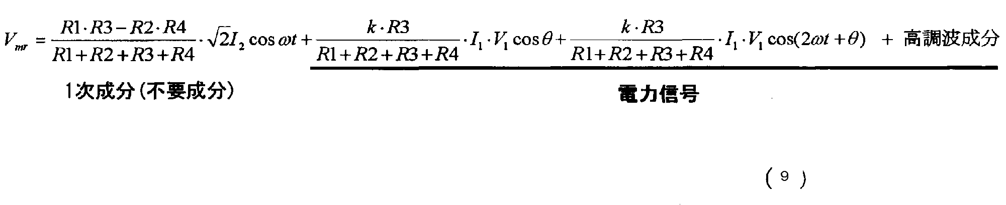
- the output signal is as shown in the following equation (1).
- the output is divided into a DC component term and an AC component term.
- A1 is an unnecessary term unrelated to the power generated by the unbalance of the bridge resistance
- A2 is a term (instantaneous power) proportional to the power.
- Patent Document 1 proposes a magnetic field sensor in which a current-carrying part is formed by opening a part of an annular pattern in order to increase sensitivity.
- Thin-film wattmeter using a magnetic film (Volume MAG-05 No. 182 of IEEJ Magnetics Study Group) Thin-film wattmeter using a magnetic film (Volume MAG-05 No. 192, Society of Electrical Engineers of Japan)
- the value of the amplitude value I 1 ⁇ V 1 of the 2 ⁇ component is measured, and the power factor cos ⁇ is separately measured and separately multiplied to obtain I 1 ⁇ V 1 ⁇ cos ⁇ .
- the power factor is not 1, it is necessary to separately measure and calculate the power factor.
- the case of a current waveform having a harmonic component there is a problem that only the power of the fundamental wave component can be extracted.
- I 2 is a device current.
- the present invention has been made in view of the above circumstances, and an object of the present invention is to provide a magnetic field sensor capable of determining a positive / negative direction and capable of highly reliable magnetic field detection. It is another object of the present invention to provide a power measuring device that can easily measure power without separately measuring the power factor.
- the magnetic field sensor of the present invention provides a voltage between a magnetic thin film, a power feeding unit having an input / output terminal for supplying an element current to the magnetic thin film, and an end of the magnetic thin film in a direction orthogonal to the direction of the element current.
- the magnetic thin film is formed so as to be symmetric with respect to the direction of the device current.
- the present invention includes the magnetic field sensor, wherein the magnetic thin film has a circular outer shape.
- the magnetic thin film is an annular body.
- the present invention includes the above magnetic field sensor, wherein the magnetic thin film is formed of a square annular body, and a power feeding unit is provided so that a current flows in a diagonal direction of the square.
- the magnetic thin film is an annular body and has a constant line width.
- the magnetic thin film includes an annular magnetic body provided with an internal magnetic thin film made of a magnetic film.
- the internal magnetic thin film includes a magnetic thin film made of the same material as the magnetic thin film.
- the internal magnetic thin film includes a magnetic thin film different from the magnetic thin film.
- the magnetic field measuring method of the present invention supplies the element current so that the pattern of the magnetic thin film is symmetric with respect to the direction of the element current, and the magnetic thin film end in a direction orthogonal to the element current supply direction.
- the magnetic field strength is measured by detecting the voltage between the parts.
- the power measuring apparatus of the present invention supplies a device current to the magnetic thin film via a resistor connected to the magnetic thin film arranged parallel to the primary conductor through which alternating current flows and the primary conductor.
- a magnetic field sensor including a power supply unit including an input / output terminal, a detection unit for detecting outputs at both ends of the magnetic thin film, and a DC component extraction unit for extracting a DC component from the output of the detection unit. It is characterized by.
- the present invention includes the power measuring device in which the magnetic field sensor is formed on the same substrate as the DC component extraction unit.
- the present invention includes the power measuring apparatus, wherein the magnetic thin film of the magnetic field sensor is formed on the substrate, and the detection unit is directly connected to a wiring pattern on the substrate.
- the magnetic field sensor includes a magnetic thin film formed on the substrate, a power supply unit including an input / output terminal that supplies an element current to the magnetic thin film, and the magnetic And a detection electrode unit that detects outputs at both ends of the thin film, and the wiring pattern includes the same conductive layer as the power supply unit and the detection electrode unit.
- the present invention includes the above power measurement device, wherein the magnetic thin film is formed so that a magnetic resistance is symmetric with respect to a direction of the element current.
- the present invention includes the power measuring apparatus, wherein the magnetic thin film is formed so that a magnetization direction coincides with a direction of the element current.
- the detection unit includes a detector formed in a direction orthogonal to the direction of the element current.
- the present invention includes the power measuring apparatus, wherein the DC component extraction unit includes an integration unit that integrates the output value every 1 / f cycles of the commercial frequency f.
- the present invention further includes a zero-cross point detection unit that detects a zero-cross point of the primary voltage of the element current, and drives the DC component extraction unit according to the output of the zero-cross point detection unit. Includes those for which timing is determined.
- the present invention includes the power measuring device including a capacitor connected in parallel to the detection unit.
- the power measurement method of the present invention uses the power measurement device described above to supply a device current so that the magnetic resistance is symmetric with respect to the direction of the device current with respect to the magnetic thin film pattern, and the device The DC component of the output generated by the current supply is taken out and used as power information.
- the magnetic field sensor used in the power measuring apparatus of the present invention includes a magnetic thin film, a power supply unit including an input / output terminal for supplying an element current to the magnetic thin film, and the magnetic sensor in a direction orthogonal to the direction of the element current. And a detecting section for detecting a voltage of the thin film (between ends), wherein the magnetic thin film is formed so that the magnetoresistance is symmetric with respect to the direction of the element current.
- the present invention includes the magnetic field sensor, wherein the magnetic thin film has a circular outer shape.
- the magnetic thin film is an annular body.
- the present invention includes the above magnetic field sensor, wherein the magnetic thin film is formed of a square annular body, and a power feeding unit is provided so that a current flows in a diagonal direction of the square.
- the magnetic thin film is an annular body and has a constant line width.
- the present invention includes the above magnetic field sensor, wherein the magnetic thin film is formed of a square annular body, and a power feeding unit is provided so that a current flows in a diagonal direction of the square.
- the magnetic thin film includes an annular magnetic body provided with an internal magnetic thin film made of a magnetic film.
- the internal magnetic thin film includes a magnetic thin film made of the same material as the magnetic thin film.
- the internal magnetic thin film includes a magnetic thin film different from the magnetic thin film.
- the element current is supplied to the pattern of the magnetic thin film so that the magnetoresistance is symmetric with respect to the direction of the element current, and is orthogonal to the element current supply direction. In this direction, the magnetic field strength is measured by detecting the voltage of the magnetic thin film (between ends).
- the magnetic field sensor of the present invention since the voltage is extracted from a point orthogonal to the element current direction with a very simple configuration, the direction of the magnetic field can be detected, there is no offset, Magnetic field detection with high reliability is possible.
- the power measuring device of the present invention by taking out the DC component of the output voltage, it is possible to take out the power directly with an extremely simple configuration without the need to separately measure the power factor.
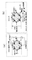
- FIG. 1 is a diagram illustrating the principle of a magnetic field sensor according to Embodiment 1 of the present invention.
- 1 is a top view of a magnetic field sensor according to a first embodiment of the present invention.
- FIG. 2 is a circuit explanatory diagram showing a measuring apparatus for measuring element characteristics of the magnetic field sensor according to Embodiment 1 of the present invention.
- FIG. 3 is a diagram illustrating the principle of a magnetic field sensor according to a second embodiment of the present invention.
- the measurement principle of the magnetic field sensor of the present invention will be described.
- the output of the ferromagnetic thin film used as the magnetic thin film is taken out in a direction orthogonal to the element current direction, and is substantially symmetric with respect to the output take-out direction.
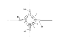
- the principle A is shown in FIG. 1, and the points A and B on the periphery of the ferromagnetic thin film pattern are symmetric with respect to the center of the pattern of the circular ferromagnetic thin film 3.
- a line segment CD that is orthogonal to the line segment AB and that passes through the center of the circle is used as an output extraction direction.
- a current I 1 is passed through a conductor 200 arranged in the ferromagnetic thin film 3 along the diameter direction thereof.
- the magnetic field vector generated by the current is H and the spontaneous magnetization vector of the element is M
- the magnetic field vector H the magnetic flux density vector obtained by combining the spontaneous magnetization vector M of the element
- the current density vector I and the magnetic flux Assuming that the angle formed by the density vector B M0 is ⁇ , the resistance between the points AB of the ferromagnetic thin film 3 is R, and the maximum resistance value between the points AB changed by the magnetic field is ⁇ R, the point CD
- the circuit configuration can be simplified because the offset is zero.
- the electric current I 1 to a conductor 200 disposed along the diameter direction in the ferromagnetic thin film 3 a magnetic field generated by the current H, the spontaneous magnetization with the device set to M, the external magnetic field
- the magnetic flux density vector obtained by combining the vector H, the spontaneous magnetization vector M of the element is B M0 , the angle formed by the current density vector I and the magnetic flux density vector B M0 is ⁇ , and the point AB between the ferromagnetic thin film 3
- the voltage V CD between the points CD can be expressed by the difference between the voltage V AC and the voltage V AD.
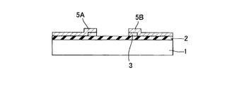
- FIG. 2 is a diagram illustrating the principle of the magnetic field sensor
- FIG. 3 is a top view
- FIG. 4 is a cross-sectional view.
- a silicon oxide film is formed as an insulating film 2 on the surface of a substrate 1 made of silicon
- an annular pattern made of a ferromagnetic thin film 3 having ferromagnetic properties is formed on the insulating film 2.
- a detection pattern formed in a direction orthogonal to the direction of the element current supplied from the power supply portions 5A and 5B along the diameter direction of the annular pattern.
- 5C and 5D conductor patterns.
- FIG. 2 the principle explanatory diagram is shown, and the points A and B on the periphery of the ferromagnetic thin film pattern are symmetrical with respect to the center of the pattern of the circular ferromagnetic thin film 3.
- a line segment CD that is orthogonal to the line segment AB and that passes through the center of the circle is used as an output extraction direction.
- the current I 1 is caused to flow through the conductor 200 disposed in the ferromagnetic thin film 3 along the diameter direction thereof.
- the magnetic field generated by the current is H and the spontaneous magnetization of the element is M
- the external magnetic field vector H the magnetic flux density vector synthesized from the spontaneous magnetization vector M of the element is B M0
- the current density vector I and the magnetic flux density Assuming that the angle formed by the vector B M0 is ⁇ , the resistance between the points AB of the magnetic thin film 3 is R, and the maximum resistance value between the points AB changed by the magnetic field is ⁇ R, between the points CD
- the voltage V CD can be expressed by a difference between the voltage V AC and the voltage V AD . Therefore, the above equation (3) is established, and when an alternating magnetic field is applied, it is possible to determine whether it is positive or negative. In addition, there is no offset when no magnetic field is applied, and the circuit configuration can be simplified because it is zero.
- the conductor pattern gold, copper, aluminum or the like is used.
- a silicon oxide film as the insulating film 2 is formed on the surface of the silicon substrate as the substrate 1, and a ferromagnetic thin film 3 is formed thereon by sputtering. At this time, sputtering is performed while applying a magnetic field so that the spontaneous magnetization directions are aligned. Then, the ferromagnetic thin film 3 is patterned by photolithography to form an annular pattern. After that, a conductive thin film such as gold is formed by sputtering, and patterned by photolithography to form power supply portions 5A and 5B and detection portions 5C and 5D as shown in FIGS. And a protective film is formed as needed and a magnetic field sensor is completed.
- the width of the magnetic thin film is reduced, so that the electrical resistance is increased and the output can be increased.
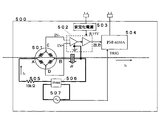
- FIG. AC is supplied from the AC power source 507 through the transformer 506 and the resistor 505 to the power feeding units A and B of the magnetic field sensor 501 shown in FIGS. 2 to 4, and the amplifier 502 is connected to the detection units C and D of the magnetic field sensor 501.
- An oscilloscope 504 as a display unit is connected to the display unit.
- Reference numeral 503 denotes a stabilized power source.
- This measuring device is housed in an iron casing 500.
- an element substrate on which this element was mounted was arranged vertically, and the measurement was performed with the distance between the element and the current line to be measured being about 3 mm.
- FIGS. 6 shows the instantaneous output when the element current I 1 is 8.842 A
- FIG. 7 shows the instantaneous output when the element current I 1 is 0 A.
- FIG. 8 shows the relationship between the current value thus obtained and the element output voltage.
- the offset by the amplifier is 5.888 V, but otherwise there is no offset and the reliability is high.
- the measurement using the element substrate arranged in the vertical direction has been described.
- the measurement may be performed by placing the electric wire to be measured on the element substrate.
- the line width is constant. If it is not constant, it is also effective to take measures such as adjusting the film thickness or adding an auxiliary pattern so that the resistance values are symmetric. Further, since the magnetic thin film has a circular outer shape and is symmetric, it can be easily formed so as to be symmetric with respect to the device current direction, and a highly reliable magnetic field sensor can be provided. In addition, by making the magnetic thin film annular, the width of the magnetic thin film is reduced, the electrical resistance is increased, the resistance value can be increased without increasing the outer shape of the element, and the output can be increased. Become.
- FIGS. 9 to 11 a circular inner shape that is similar to the inner circumference of the ring of the ferromagnetic thin film 3 constituting the annular pattern of the magnetic field sensor of the first embodiment.
- a feature is that an auxiliary pattern 4 of a ferromagnetic thin film is formed as a magnetic thin film.
- FIG. 9 is an explanatory diagram of the principle of the magnetic field sensor
- FIG. 10 is a top view
- FIG. 11 is a cross-sectional view.
- This magnetic field sensor is basically the same as in the first embodiment, but the presence of the auxiliary pattern 4 increases the magnetic sensitivity while keeping the electrical resistance high.
- the outer annular pattern and the inner auxiliary pattern 4 are not in electrical contact.
- the electrical resistance is the same as that of the magnetic field sensor of the first embodiment.
- the space is magnetically filled with the magnetic thin film, more magnetic flux can be guided and high sensitivity can be achieved. Can do.
- the sensitivity can be further increased by providing the internal magnetic thin film electrically independently in order to improve only the magnetic sensitivity while increasing the electrical resistance.
- the element structure As the element structure, as shown in FIG. 12, after forming a magnetic thin film pattern, the entire substrate surface is covered with a protective insulating film 16 made of polyimide resin, and the power supply portion 5A is formed through a through hole. 5B and detectors 5C and 5D may be formed. According to this configuration, it is possible to provide a highly reliable magnetic field sensor that prevents deterioration of the magnetic thin film.
- auxiliary pattern formed inside the annular pattern may be made of the same material, or the auxiliary pattern 24 may be formed of a magnetic thin film made of another material as shown in FIG. .
- the internal magnetic thin film that is, the auxiliary pattern with a magnetic thin film made of the same material as the magnetic thin film
- the sensitivity can be adjusted by configuring the internal magnetic thin film, that is, the auxiliary pattern, with a magnetic thin film different from the magnetic thin film. Further, when a large number of magnetic field sensors are arranged side by side, it is possible to adjust the sensitivity by adjusting the material of the internal magnetic thin film in order to align the sensitivity.
- the protective film it is possible to use an organic film such as a polyimide resin or a novolac resin in addition to an inorganic film such as a silicon oxide film or aluminum oxide.
- the ferromagnetic thin film is composed of a square annular pattern 33, and power supply portions 5 ⁇ / b> A and 5 ⁇ / b> B are provided so that current flows in the diagonal direction of the square.
- the detection units 5C and 5D are formed in a direction orthogonal to.
- only the square annular pattern 33 is formed in place of the annular pattern 3 of the magnetic field sensor of the first embodiment, and other configurations are the same as those of the first embodiment, and will be described here. Is omitted. The same symbols are assigned to the same parts.
- FIG. 14 is a diagram illustrating the principle of this magnetic field sensor
- FIG. 15 is a top view.
- the magnetic flux density vector is a combination of the spontaneous magnetization vector M and the external magnetic field vector H possessed by the element, and when there is no external magnetic field, the magnetic flux density vector becomes the spontaneous magnetization vector direction.
- the external magnetic field is an alternating magnetic field, it vibrates in the vertical direction in the figure around the spontaneous magnetization vector.
- the output Vmr of the sensor can be expressed by the following equation.
- the angle formed by the current density vector and the magnetic flux density vector is ⁇ 1 , ⁇ 2
- the angle formed by AB and AC and AB and AD is ⁇
- the voltage between AC when there is no external magnetic field is The voltage between V AC0 and AD is V AD0
- the maximum value of voltage change due to the magnetoresistive effect is ⁇ Vr.
- the output is smaller than that of the square.
- the magnetic thin film is formed by the sputtering method.
- the magnetic thin film is not limited to the sputtering method, and can be formed by a vacuum deposition method, a coating method, a dipping method, or the like.
- the substrate in addition to a semiconductor substrate such as silicon, an inorganic substrate such as sapphire, glass or ceramic, or an organic substrate such as resin may be used. Among these, it is particularly preferable to use a thin and light material excellent in so-called flexibility.
- a substrate similar to a plastic film widely used as a printed wiring board or the like can be used. More specifically, various known materials as plastic film materials, such as polyimide, polyethylene terephthalate (PET), polypropylene (PP), and Teflon (registered trademark) can be used.
- PET polyethylene terephthalate
- PP polypropylene
- Teflon registered trademark
- a flexible substrate it can be arranged so as to have a higher sensitivity, for example, arranged so as to surround the electric wire to be measured. In consideration of bonding with solder, a polyimide film having high heat resistance may be used.
- the thickness of the substrate is not particularly limited, but is preferably about 1 to 300 ⁇ m.
- a magnetic thin film pattern may be formed directly on a substrate such as a glass substrate to form a magnetic field sensor, but once a chip is formed, this is applied to a glass substrate or a printed wiring board using a wire bonding method, You may make it mount by the flip-chip method. Further, by integrating the processing circuit in the chip, it becomes possible to provide a magnetic field sensor with higher accuracy and reliability.
- the present invention is not limited to the above embodiment, and the magnetic thin film is formed so that the output extraction direction of the magnetic thin film is perpendicular to the element current direction and the magnetoresistance is symmetric with respect to the element current direction.
- the circuit configuration can be simplified because it is possible to determine whether the direction is positive or negative, and there is no offset when no magnetic field is applied.
- the magnetic field sensor using a ferromagnetic thin film was used in the said embodiment, you may use another magnetic field sensor, without being limited to this.
- This power measurement device uses the planar Hall effect, which is a phenomenon in which the electrical resistance value of a magnetic material changes depending on the angle between current and magnetization in a ferromagnetic material, and can obtain linear characteristics without a bias magnetic field. Attention is focused on extracting signal components proportional to power. 16 and 17 illustrate this measurement principle.
- FIG. 16 is a schematic explanatory diagram of this power measuring apparatus, and FIG. 17 is an equivalent circuit diagram.
- the magnetic field sensor used here is an element that converts a change in an external magnetic field into an electric signal.
- the ferromagnetic thin film 5 as a magnetic field detection film is patterned, and a current is passed through the pattern of the magnetic field detection film to change the external magnetic field as a voltage change. Is converted into an electrical signal.
- the ferromagnetic thin film can be regarded as a resistance bridge composed of R 1 , R 2 , R 3 , and R 4 .
- FIG. 18 is an explanatory diagram of this power measuring device
- FIG. 19 is a sectional view
- FIG. 20 shows the output of this power measuring device.
- This power measuring device is connected to the primary thin film, which is arranged in parallel to the primary conductor through which alternating current flows, and to the primary thin film, and to supply an element current to the ferromagnetic thin film via a resistor.
- the magnetic field sensor 10 provided with the electric power feeding part provided with the output terminal, the detection part which detects the output of the said ferromagnetic thin film both ends, and the direct-current component extraction part 50 which extracts a direct-current component from the output of the said detection part were provided. It is characterized by that.
- the power supply unit of the magnetic field sensor 10 is connected to the AC power supply 8 via a resistor 9 as a load.
- the DC component extraction unit 50 connected to the detection unit includes an amplifier 20, an A / D converter 30, and a CPU 40.
- the power measuring device includes a magnetic field sensor 10 mounted on a circuit board 1 made of a printed wiring board via a wiring pattern 3P, and a chip component solder-connected to the wiring pattern 3P on the printed wiring board.
- the amplifier 20, the A / D converter 30, and the CPU 40 are connected.
- Reference numeral 2 denotes an insulating film.
- the magnetic field sensor is formed on the circuit board 1 together with the DC component extraction unit 50, the surface S surrounded by the ferromagnetic thin film of the magnetic field sensor and the input line of the amplifier 20 is the primary conductor current. does not cross the magnetic flux generated by I 1, it is possible to reduce the influence of unwanted inductive Symbol power by magnetic flux linkage. Further, the thickness and size can be reduced.
- the linear characteristics can be obtained without a bias magnetic field by utilizing the planar Hall effect, which is a phenomenon in which the electrical resistance value of the magnetic material changes depending on the angle between the current and the magnetization in the ferromagnetic material. Focusing on the points that can be obtained, the signal component proportional to the power is extracted, and the DC component extraction unit extracts the DC component from the output of the detection unit, so the extracted waveform is current x voltage x force Since it is a rate component, it is electric power and can be directly measured without multiplication from the waveform, so that it is possible to easily and accurately detect electric power.
- the ferromagnetic thin film is formed so that a magnetic resistance is symmetric with respect to a direction of the element current.
- the maximum value of the Vmr output can be increased, and the S / N ratio as the system can be increased. improves. Therefore, according to the above configuration, high-accuracy power measurement can be performed.
- the ferromagnetic thin film is preferably formed so that the magnetization direction coincides with the direction of the element current from the viewpoint of increasing sensitivity.
- a planar hole effect that is, a magnetoresistance effect (a phenomenon in which a resistance value changes due to a magnetic field) occurs in the ferromagnetic thin film.
- FIG. 21 shows the relationship between the current I 2 vector, the direction of spontaneous magnetization, that is, the magnetic field H by the primary conductor, and the synthesized magnetic flux density vector BMO . From this figure, therefore, by setting the direction of the spontaneous magnetization parallel to the direction of the element current I 2 as shown in FIGS.
- FIGS. 21A and 21B the positive maximum value in the magnetic field direction by the primary conductor and the negative At the minimum value, the output (absolute value) is equal and the dynamic range can be maximized.
- the lower part of FIGS. 21A and 21B is an explanatory diagram showing the generation of the upper-layer combined magnetization.
- FIGS. 21C to 21D if the value is not parallel, either the positive maximum value or the negative minimum value (absolute value) becomes small, and the dynamic range of the sensor becomes narrow.
- FIG. 22 shows the dynamic range as a bold line in the figure in terms of the element output and the magnetic field intensity by the primary conductor. For dynamic range defined by whichever of the positive and negative sides of the element output small, whole since the positive side and the negative side become equal when the device current vector I 2 and spontaneous magnetization is set to be parallel The dynamic range is the most effective.
- a linear characteristic can be obtained without a bias magnetic field by utilizing the planar Hall effect, which is a phenomenon in which the electrical resistance value of the magnetic material changes depending on the angle between current and magnetization in the ferromagnetic material.
- the DC component is extracted from the output of the detection unit by the DC component extraction unit so that the signal component proportional to the power is extracted, so the extracted waveform is current ⁇ voltage ⁇ power factor component. Therefore, since it is electric power and can be measured directly without multiplication from the waveform, it is possible to easily and accurately detect electric power.
- the detection unit is formed in a direction orthogonal to the direction of the element current, as shown in the explanatory diagrams of FIGS.
- FIG. 24A shows a case where the external magnetic field vector H is zero
- FIG. 24B shows a case where the external magnetic field vector H forms an angle of ⁇ / 4.
- the DC component extraction unit 50 includes an integration unit that integrates the output value every 1 / f cycles of the commercial frequency f.
- Vmr is a common multiple of the direct current component + commercial frequency. Therefore, as shown in FIG. 25 for one cycle of the output value when the power of the power measuring device is taken as output, If integration is performed during the period, plus and minus are canceled out for the AC component, and only the DC component can be extracted.
- the direct current component can be obtained in units of cycles and is suitable for high-speed computation, so it has excellent transient response. Further, by integrating with a period, the first-order unnecessary terms can be dropped, and even harmonic components of power can be extracted.
- a zero-cross point detection unit 60 and a cycle determination unit 70 are connected to the detection unit of the magnetic field sensor 10, and output by the cycle determination unit 70 based on the output of the zero-cross point detection unit.
- the period is detected.
- the period is determined by the period determination unit 70 according to the output of the zero cross point detection unit 60, and the driving timing of the DC component extraction unit 50 is determined by this period. Since other configurations are the same as those of the fourth embodiment, description thereof is omitted here.
- a capacitor 80 is connected in parallel to the detection unit of the magnetic field sensor. Since other configurations are the same as those of the fourth embodiment, description thereof is omitted here. According to this configuration, by smoothing the Vmr signal with the capacitor, the DC component can be taken out in a short period less than the cycle, so that the power value can be obtained at high speed and the DC component can be detected with a simple circuit configuration. It becomes possible to do.
- the magnetic field sensor is composed of chip parts and mounted on the printed wiring board constituting the circuit board.
- the pattern of the direct ferromagnetic thin film 3 on the printed wiring board 1 constituting the circuit board is used.
- a conductor pattern that forms the power supply unit and the detection unit is formed and integrated in the same process as the wiring pattern.
- the amplifier, the A / D converter, and the CPU are composed of chip parts.
- a processing circuit can be integrated on a silicon substrate, and a magnetic field sensor can be formed through an insulating film to form a monolithic element. According to this configuration, it is possible to make the device thinner and smaller.
- the magnetic field sensors described in the second to third embodiments may also be used in the power measurement devices described in the fourth to seventh embodiments.
- the magnetic field sensor and the processing circuit can be integrated with the substrate, and further reduction in thickness and size can be achieved.
- the magnetic field sensor includes a magnetic thin film formed on the substrate, a power supply unit having an input / output terminal for supplying an element current to the magnetic thin film, and detection for detecting outputs at both ends of the magnetic thin film. It may comprise an electrode part, and a wiring pattern may comprise the same conductor layer as the power feeding part and the detection electrode part. According to this configuration, since it is only necessary to form a pattern of the magnetic thin film in addition to the configuration of the normal circuit board, it can be formed very easily.
- the magnetic thin film may be formed so that the magnetoresistance is symmetric with respect to the direction of the element current. According to this configuration, since the magnetoresistance is symmetric with respect to the direction of the element current, the maximum value of the Vmr output can be increased, and the S / N ratio as a system is improved.
- the power measurement device may include a capacitor connected in parallel to the detection unit. According to this configuration, by smoothing the Vmr signal with the capacitor, the DC component can be taken out in a short period less than the cycle, so that the power value can be obtained at high speed and the DC component can be detected with a simple circuit configuration. It becomes possible to do.
- a step of supplying an element current so that the magnetoresistance is symmetric with respect to the direction of the element current with respect to the magnetic thin film pattern, and an output generated by the supply of the element current The direct current component is extracted and used as power information. According to this configuration, it is not necessary to separately measure the power factor, it can be easily measured, and the error is reduced as compared with the case of integration.
- the magnetic field sensor detects a voltage of the magnetic thin film (between end portions) in a direction orthogonal to the direction of the element current, and a power feeding unit having an input / output terminal for supplying an element current to the magnetic thin film.
- the magnetic thin film may be formed so that the magnetoresistance is symmetric with respect to the direction of the element current. According to this configuration, the output direction of the magnetic thin film is set to a direction orthogonal to the element current direction, and the magnetic resistance is symmetric with respect to the element current direction, so that the positive / negative of the direction is determined.
- the circuit configuration can be simplified.
- the element current is supplied to the pattern of the magnetic thin film so that the magnetoresistance is symmetric with respect to the direction of the element current, and is orthogonal to the element current supply direction.
- the magnetic field strength is measured by detecting the voltage of the magnetic thin film (between ends).
- the output direction of the magnetic thin film is set to a direction orthogonal to the element current direction, and the magnetic resistance is symmetric with respect to the element current direction, so that the positive / negative of the direction is determined.
- the circuit configuration can be simplified.
- the magnetic field sensor of the present invention it is possible to detect the magnetic field strength with high accuracy, and therefore it can be applied to a current sensor, a power sensor, and the like.
- the power measuring device of the present invention correct power measurement can be performed even when the power factor is not 1 or even a load including harmonic current, and a current sensor such as a current transformer is used. Since it is possible to reduce the size and cost as compared with the conventional power measuring device, it can be applied to various energy saving tools.
- Substrate 2 Insulating film 3, 33 Ferromagnetic thin film ((annular) pattern) 4, 24 Auxiliary pattern 5A, 5B Power supply unit 5C, 5D Detection unit 100 Ferromagnetic thin film 200 Conductor
Abstract
Description
使用した電力を円盤の回転数に変換し積算演算を行うという既存の積算電力計に、回転を検出するセンサを付加する、あるいは、電流計(CT)、電圧計(PT)を新たに付加し、電子回路やマイクロプロセッサによる乗算計算を行い、電力を計測するなどの方法を用いた電力計が使用されている。しかし、このような電力計は、装置が大型化するだけでなく、高価なものとなり、また、余計なエネルギーを消費しかねないという状況である。
そこで消費電力をそのまま電気量として測定することができるとともに、小型化および集積化の可能な電力計の開発が望まれている。
ここで用いられる磁界センサは、外部磁界の変化を電気信号に変換する素子であり、強磁性薄膜や半導体薄膜等の磁性薄膜をパターニングし、その磁性薄膜のパターンに電流を流し電圧変化として外部磁界の変化を電気信号に変換するものである。
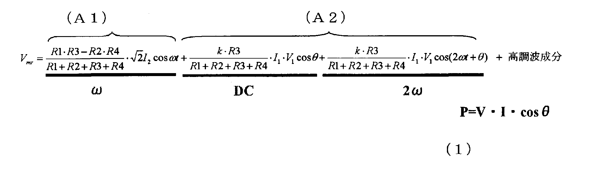
A1はブリッジ抵抗のアンバランスで生ずる電力と関係のない不要な項、A2は電力に比例する項(瞬時電力)である。
点A-B間の電圧VABは
VAB=I2(R+ΔRcos2θ) (2)
となる。ここでI2は素子電流である。
本発明は前記実情に鑑みてなされたもので、正負方向の判定が可能で、信頼性の高い磁界検出を可能にする磁界センサを提供することを目的とする。
また、力率を別途計測することなく、簡単に電力を計測することができる電力計測装置を提供することを目的とする。
本発明の実施の形態の説明に先立ち、本発明の磁界センサの測定原理について説明する。
本発明の磁界センサでは、磁性薄膜として用いる強磁性薄膜に対し、素子電流方向に対し直交する方向に出力取り出しを行うようにするとともに、出力取り出し方向に対してほぼ対称となるようにしている。
これを数式化すると、
VCD=I2(ΔRsin2θ) (3)
で表すことができる。ここでI2は素子電流である。
つまり交流磁界を印加した時、正負を判定することができる。
この構成によれば、強磁性薄膜3にその直径方向に沿って配置された導体200に電流I1を流し、その電流によって生じる磁界をH、素子の持つ自発磁化をMとしたとき、外部磁界ベクトルH、素子の持つ自発磁化ベクトルMを合成した磁束密度ベクトルをBM0とするとともに電流密度ベクトルIと磁束密度ベクトルBM0のなす角をθと、強磁性薄膜3の点A-B間の抵抗をR、磁界によって変化する点A-B間の抵抗値の最大値をΔRとすると、点C-D間の電圧VCDは、電圧VACと電圧VADとの差で表すことができる。
本実施の形態1の磁界センサについて説明する。図2にこの磁界センサの原理説明図、図3に、上面図、図4に断面図を示す。この磁界センサは図3及び4に示すように、シリコンからなる基板1表面に絶縁膜2として酸化シリコン膜を形成し、この絶縁膜2上に強磁性特性を有する強磁性薄膜3からなる環状パターンを形成し、この環状パターンの直径方向に沿って給電部5A、5Bを構成する導体パターン、および、この給電部5A、5Bから供給される素子電流の方向に直交する方向に形成された検出部5C、5Dとしての導体パターンとを具備したものである。
従って前記式(3)が成り立ち、交流磁界を印加した時、正負を判定することができる。
また、磁界を印加しないときのオフセットがなく、ゼロとなるため回路構成を簡単にすることができる。
また導体パターンとしては金、銅、アルミニウムなどが用いられる。
基板1としてのシリコン基板表面に、絶縁膜2としての酸化シリコン膜を形成し、この上層に、スパッタリング法により、強磁性薄膜3を形成する。このとき、磁界を印加しつつスパッタリングを行い、自発磁化方向が揃うように形成する。
そして、フォトリソグラフィによりこの強磁性薄膜3をパターニングし、円環状のパターンとする。
こののち、スパッタリング法により、金などの導電体薄膜を形成し、フォトリソグラフィによりパターニングし、図3及び図4に示すような給電部5A、5Bおよび検出部5C、5Dを形成する。
そして必要に応じて保護膜を形成し、磁界センサが完成する。
この測定結果を、図6および図7に示す。図6は素子電流I1を8.842Aとしたときの瞬時出力であり、図7は素子電流I1を0Aとしたときの瞬時出力である。
また、磁性薄膜は、外形が円形であり、対称形であるため、素子電流方向に対して対称となるように形成しやすく、信頼性の高い磁界センサを提供することが可能となる。
また、磁性薄膜を環状とすることで、磁性薄膜の幅が小さくなり、電気抵抗が増大し、素子の外形を大きくすることなく抵抗値を大きくすることができ、出力を大きくすることが可能となる。
次に、本発明の実施の形態2について説明する。本実施の形態では、図9乃至図11に示すように、前記実施の形態1の磁界センサの環状パターンを構成する強磁性薄膜3の環の内周に沿って相似形である円状の内部磁性薄膜として強磁性薄膜の補助パターン4を形成したことを特徴とするものである。
構成としてはこの補助パターン4が付加されただけで、他の構成については前記実施の形態1と同様であり、ここでは説明を省略する。同一部位には同一符号を付した。ここで図9はこの磁界センサの原理説明図、図10に上面図、図11に断面図を示す。この磁界センサは基本的には前記実施の形態1と同様であるが、この補助パターン4の存在により、電気抵抗は高めたままで磁気的な感度を高めるようにしたものである。強磁性薄膜3のうち外側の環状パターンと内部の補助パターン4とは電気的に接触していない。このため、電気抵抗は前記実施の形態1の磁界センサと同様であるが、磁気的には空間部が磁性薄膜で埋められるため、より多くの磁束を導くことができ、高感度化を図ることができる。
このように、本実施の形態によれば、磁性体の間に空間が形成されるため、外部磁界に対する感度が低下する。そこで電気抵抗を高めたままで、磁気的な感度のみを向上すべく、電気的に独立して内部磁性薄膜を設けたことで、より高感度化を図ることができる。
次に、本発明の実施の形態3について説明する。本実施の形態では、図14および15に示すように、強磁性薄膜は、正方形の環状パターン33で構成され、前記正方形の対角線方向に電流が流れるように給電部5A、5Bが設けられ、これらに直交する方向に検出部5C、5Dが形成されたことを特徴とする。
本実施の形態でも、前記実施の形態1の磁界センサの環状パターン3に代えて正方形の環状パターン33を形成しただけで、他の構成については前記実施の形態1と同様であり、ここでは説明を省略する。同一部位には同一符号を付した。ここで図14はこの磁界センサの原理説明図、図15は、上面図である。
ただし、前述したのと同様に、電流密度ベクトルと磁束密度ベクトルのなす角をθ1、θ2、ABとACおよびABとADのなす角をφ、外部磁界がない時のAC間の電圧をVAC0、AD間の電圧をVAD0、磁気抵抗効果による電圧変化の最大値をΔVrとする。

また前記実施の形態では強磁性薄膜を用いた磁界センサを用いたが、これに限定されることなく他の磁界センサを用いてもよい。
本発明の実施の形態の説明に先立ち、本発明の測定原理について説明する。
この電力計測装置では、強磁性体内において、電流と磁化のなす角度によりその磁性体の電気抵抗値が変わる現象であるプレーナホール効果を利用し、バイアス磁界なしで線形特性を得ることができる点に着目し、電力に比例する信号成分を取り出すようにしている。図16および17にこの測定原理を示す。図16はこの電力測定装置の概要説明図、図17は等価回路図である。
ここで用いられる磁界センサは、外部磁界の変化を電気信号に変換する素子であり、磁界検出膜としての強磁性薄膜5をパターニングし、その磁界検出膜のパターンに電流を流し電圧変化として外部磁界の変化を電気信号に変換するものである。
ここで図17に示すように、強磁性薄膜はR1、R2、R3、R4からなる抵抗ブリッジとみなすことができる。

すなわち、抵抗ブリッジが零磁界でVmr=0の場合(R1=R2=R3=R4)、印加磁界により現れる出力Vmrは抵抗変化率に比例する。
抵抗変化率ΔR1/R1はI1に比例し、強磁性薄膜にかかる電圧VbはI2に比例するよう設計可能であるため、Vmr出力はI1とI2の積に比例する。すなわち電力に比例する信号成分である。I1とI2を瞬時式に展開すると、Vmrは、(DC項)+(2ω項)である。
本発明の電力計測装置で用いられる磁界センサについては、実施の形態1で説明したのでここでは説明を省略する。
また、この電力計測装置は、プリント配線基板からなる回路基板1上に配線パターン3Pを介して実装された磁界センサ10と、このプリント配線基板上の配線パターン3Pに半田接続されたチップ部品からなるアンプ20と、A/D変換器30と、CPU40とが接続されて構成されている。2は絶縁膜である。
また薄型化および小型化が可能となる。
本実施の形態の電力計測装置によれば、強磁性体内において、電流と磁化のなす角度によりその磁性体の電気抵抗値が変わる現象であるプレーナホール効果を利用し、バイアス磁界なしで線形特性を得ることができる点に着目し、電力に比例する信号成分を取り出すようにし直流成分抽出部によって、検出部の出力から直流成分を抽出するようにしているため、抽出した波形は電流×電圧×力率成分となっているため、電力であり、波形から掛け算をすることなく直接計測することができるため、容易でかつ高精度の電力検出が実現可能である。
としたとき、θ=π/4の磁界印加のときにVmrは最大値をとるが、出力取り出し点において対称である構成のときに最も効率よく信号を取り出すことができる。このように上記構成によれば、素子電流の方向に対して磁気抵抗が対称となるように形成されているため、Vmr出力の最大値を大きく取ることができ、システムとしてのS/N比が向上する。
従って上記構成によれば、高精度の電力計測が可能となる。
このように、自発磁化をもたせることにより、強磁性薄膜に、プレーナホール効果すなわち磁気抵抗効果(磁界により抵抗値が変化する現象)が生ずる。ここで電流I2ベクトルと、自発磁化の方向すなわち一次導体による磁界Hと、合成された磁束密度ベクトルBMOとの関係を図21に示す。この図から、従って自発磁化の方向を図21(a)および(b)に示すように素子電流I2の方向に平行としておくことにより、一次導体による磁界方向で正の最大値と、負の最小値で出力(絶対値)が等しくなりダイナミックレンジを最大にすることができる。図21(a)および(b)の下段は上断の合成磁化の生成を示す説明図である。一方、図21(c)乃至(d)に示すように平行でなければ正の最大値と、負の最小値(絶対値)のいずれかが小さくなるため、センサのダイナミックレンジが狭くなる。図22は素子出力と一次導体による磁界強度において、ダイナミックレンジを図中太線で示したものである。ダイナミックレンジは素子出力の正側と負側のいずれか小さい方で規定されるために、素子電流ベクトルI2と自発磁化が平行になるようにした場合に正側と負側が等しくなるので全体のダイナミックレンジが最も有効に取り得るものとなる。
ここで図24(a)は外部磁界ベクトルHがゼロの時、図24(b)は外部磁界ベクトルHがπ/4の角度をなすときであるときを示す。
この構成によれば、θ=π/4の磁界印加のときにVmrは最大値をとるため、出力取り出し点において対称である構成のときに最も効率よく信号を取り出すことができる。
上記構成によれば、Vmrは、直流成分+商用周波数の公倍数であるから、図25にこの電力計測装置の電力を出力としてとりだしたときの出力値の1周期分を示すように、商用周波数の周期期間中積算すれば交流分はプラスマイナスが相殺されて直流分だけを取り出すことができる。直流成分を周期単位で得ることができ高速演算に適うので、過渡応答性に優れる。また、周期で積算することで、1次の不要な項を落とすことができ、電力の高調波成分まで取り出すことができる。
次に本発明の実施の形態5について説明する。
本実施の形態では、図26に示すように、磁界センサ10の検出部にゼロクロス点検出部60および周期判定部70を接続し、このゼロクロス点検出部の出力に基づいて周期判定部70で出力の周期を検出するようにしたことを特徴とするものである。ここではゼロクロス点検出部60の出力に応じて、周期判定部70で周期が判定され、この周期によって前記直流成分抽出部50の駆動タイミングが決定される。他の構成については前記実施の形態4と同様であるため、ここでは説明を省略する。
この構成によれば、系統周波数は常時変動しているので周期を正しく測るには系統電圧を用いるのが最も精度が良く、素子電流I2のために電圧信号を基板に取り込んでいる箇所を分岐することで、新規に外部電圧信号線を施すことなく電圧信号から周期を検出することが可能となる。
次に本発明の実施の形態6について説明する。
本実施の形態では、図27に示すように、電力計測装置において、磁界センサの検出部にコンデンサ80を並列接続したものである。他の構成については前記実施の形態4と同様であるため、ここでは説明を省略する。
この構成によれば、コンデンサでVmr信号を平滑化することで、周期未満の短期間で直流成分を取り出すことができるので高速で電力値を得ることができ、直流成分を簡単な回路構成で検出することが可能となる。
次に本発明の実施の形態7について説明する。
前記実施の形態4では磁界センサはチップ部品で構成し、回路基板を構成するプリント配線基板に搭載するようにしたが、回路基板を構成するプリント配線基板1上の直接強磁性薄膜3のパターンを形成し、給電部および検出部を構成する導体パターンを配線パターンと同一工程で形成し、集積化したものである。そして増幅器やA/D変換器、CPUはチップ部品で構成する。あるいはシリコン基板上に処理回路を集積化するとともに、絶縁膜を介して磁界センサを形成し、モノリシック素子とすることも可能である。
この構成によれば、より薄型化小型化が可能となる。
なお、前記実施の形態4乃至7で説明した電力計測装置においても、前記実施の形態2乃至3で説明した磁界センサを用いてもよいことはいうまでもない。
この構成によれば、通常の回路基板の構成に加えて、磁性体薄膜のパターンを形成するだけでよいため、極めて容易に形成可能である。
この構成によれば、素子電流の方向に対して磁気抵抗が対称となるように形成されているため、Vmr出力の最大値を大きく取ることができ、システムとしてのS/N比が向上する。
この構成によれば、コンデンサでVmr信号を平滑化することで、周期未満の短期間で直流成分を取り出すことができるので高速で電力値を得ることができ、直流成分を簡単な回路構成で検出することが可能となる。
この構成によれば、力率を別途計測する必要がなく、簡単に計測することができ、かつ積算による場合に比べ、誤差も低減される。
この構成によれば、磁性薄膜の出力取り出し方向を素子電流方向に対し直交する方向とするとともに、素子電流の方向に対して磁気抵抗が対称となるように形成することで、方向の正負を判定することができ、かつ磁界を印加しないときのオフセットがなくなるため回路構成を簡単にすることができる。
この構成によれば、磁性薄膜の出力取り出し方向を素子電流方向に対し直交する方向とするとともに、素子電流の方向に対して磁気抵抗が対称となるように形成することで、方向の正負を判定することができ、かつ磁界を印加しないときのオフセットがなくなるため回路構成を簡単にすることができる。
また、本発明の電力計測装置によれば、力率が1でない場合あるいは高調波電流が含まれた負荷であっても正しい電力計測を行うことができ、変流器などの電流センサを用いた従来の電力計測装置に比較して小型化、低いコスト化が可能となることから、種々の省エネツールに適用可能である。
2 絶縁膜
3、33 強磁性薄膜((環状)パターン)
4、24 補助パターン
5A、5B 給電部
5C、5D 検出部
100 強磁性薄膜
200 導体
Claims (20)
- 磁性薄膜と、
前記磁性薄膜に素子電流を供給する入出力端子を備えた給電部と、
前記素子電流の方向に直交する方向における前記磁性薄膜端部間の電圧を検出する検出部とを具備し、
前記磁性薄膜は、前記素子電流の方向に対して対称となるように形成された磁界センサ。 - 請求項1に記載の磁界センサであって、
前記磁性薄膜は、外形が円形である磁界センサ。 - 請求項1または2に記載の磁界センサであって、
前記磁性薄膜は、環状体である磁界センサ。 - 請求項3に記載の磁界センサであって、
前記磁性薄膜は、正方形の環状体で構成され、前記正方形の対角線方向に電流が流れるように給電部が設けられた磁界センサ。 - 請求項3に記載の磁界センサであって、
前記磁性薄膜は、線幅が一定である磁界センサ。 - 請求項2乃至5のいずれか1項に記載の磁界センサであって、
前記磁性薄膜は、前記環状体の内部に、磁性膜からなる内部磁性薄膜が設けられた磁界センサ。 - 請求項6に記載の磁界センサであって、
前記内部磁性薄膜は、前記磁性薄膜と同一材料からなる磁性薄膜で構成された磁界センサ。 - 請求項6に記載の磁界センサであって、
前記内部磁性薄膜は、前記磁性薄膜と異なる磁性薄膜で構成された磁界センサ。 - 磁性薄膜のパターンが、
素子電流の方向に対して対称となるように、素子電流を供給し、
前記素子電流の供給方向に直交する方向で、前記磁性薄膜端部間の電圧を検出することで磁界強度を測定する磁界測定方法。 - 交流が流れる一次導体に対し、平行となるように配置された磁性薄膜と、
前記一次導体に接続され、前記磁性薄膜に抵抗体を介して素子電流を供給する入出力端子を備えた給電部と、
前記磁性薄膜両端の出力を検出する検出部とを具備した磁界センサと、
前記検出部の出力から直流成分を抽出する直流成分抽出部とを具備した電力計測装置。 - 請求項10に記載の電力計測装置であって、
前記磁界センサは、前記直流成分抽出部と同一基板上に形成された電力計測装置。 - 請求項11に記載の電力計測装置であって、
前記磁界センサの前記磁性薄膜は、前記基板上に成膜され、前記検出部が前記基板上の配線パターンと直接接続された電力計測装置。 - 請求項11に記載の電力計測装置であって、
前記磁界センサは、
前記基板上に成膜された磁性薄膜と、
前記磁性薄膜に素子電流を供給する入出力端子を備えた給電部と、
前記磁性薄膜両端の出力を検出する検出電極部とを具備し、
前記配線パターンが前記給電部と前記検出電極部と同一の導体層で構成された電力計測装置。 - 請求項13に記載の電力計測装置であって、
前記磁性薄膜は、前記素子電流の方向に対して磁気抵抗が対称となるように形成された電力計測装置。 - 請求項10乃至14のいずれか1項に記載の電力計測装置であって、
前記磁性薄膜は、磁化方向が前記素子電流の方向と一致するように形成された電力計測装置。 - 請求項10乃至15のいずれか1項に記載の電力計測装置であって、
前記検出部は、前記素子電流の方向に直交する方向に形成された電力計測装置。 - 請求項10乃至16のいずれか1項に記載の電力計測装置であって、
前記直流成分抽出部は、出力値を商用周波数fのf分の1の周期毎に積算する積算部を具備した電力計測装置。 - 請求項10乃至16のいずれか1項に記載の電力計測装置であって、
前記素子電流の一次電圧のゼロクロス点を検出するゼロクロス点検出部を具備し、
前記ゼロクロス点検出部の出力に応じて、前記直流成分抽出部の駆動タイミングが決定される電力計測装置。 - 請求項18に記載の電力計測装置であって、
前記検出部に並列接続されたコンデンサを具備した電力計測装置。 - 請求項10乃至19のいずれか1項に記載の電力計測装置を用い、
磁性薄膜のパターンに対し、
素子電流の方向に対して磁気抵抗が対称となるように、素子電流を供給する工程と、
前記素子電流の供給によって生起された出力の直流成分を取り出し、電力情報とする電力計測方法。
Priority Applications (4)
| Application Number | Priority Date | Filing Date | Title |
|---|---|---|---|
| US13/392,352 US20120229131A1 (en) | 2009-08-26 | 2010-08-26 | Magnetic field sensor, as well as magnetic field measurement method, power measurement device, and power measurement method using the same |
| CN201080038072.5A CN102656471B (zh) | 2009-08-26 | 2010-08-26 | 磁场传感器、使用其的磁场测定方法、电力测量装置及电力测量方法 |
| KR1020127004915A KR101314365B1 (ko) | 2009-08-26 | 2010-08-26 | 자계 센서, 이것을 이용한 자계 측정 방법, 전력 계측 장치 및 전력 계측 방법 |
| EP10811972.8A EP2461174A4 (en) | 2009-08-26 | 2010-08-26 | MAGNETIC FIELD SENSOR, AND MAGNETIC FIELD MEASURING METHOD, ENERGY MEASURING DEVICE, AND ENERGY MEASURING METHOD USING THE SAME |
Applications Claiming Priority (4)
| Application Number | Priority Date | Filing Date | Title |
|---|---|---|---|
| JP2009195104A JP5620076B2 (ja) | 2009-08-26 | 2009-08-26 | 電力計測装置 |
| JP2009-195104 | 2009-08-26 | ||
| JP2009195103A JP5620075B2 (ja) | 2009-08-26 | 2009-08-26 | 磁界センサおよびこれを用いた磁界測定方法 |
| JP2009-195103 | 2009-08-26 |
Publications (1)
| Publication Number | Publication Date |
|---|---|
| WO2011024923A1 true WO2011024923A1 (ja) | 2011-03-03 |
Family
ID=43628022
Family Applications (1)
| Application Number | Title | Priority Date | Filing Date |
|---|---|---|---|
| PCT/JP2010/064532 WO2011024923A1 (ja) | 2009-08-26 | 2010-08-26 | 磁界センサ、これを用いた磁界測定方法、電力計測装置および電力計測方法 |
Country Status (6)
| Country | Link |
|---|---|
| US (1) | US20120229131A1 (ja) |
| EP (1) | EP2461174A4 (ja) |
| KR (1) | KR101314365B1 (ja) |
| CN (1) | CN102656471B (ja) |
| TW (1) | TWI480566B (ja) |
| WO (1) | WO2011024923A1 (ja) |
Cited By (1)
| Publication number | Priority date | Publication date | Assignee | Title |
|---|---|---|---|---|
| JP5885209B2 (ja) * | 2011-02-01 | 2016-03-15 | 公立大学法人大阪市立大学 | 電力計測装置 |
Families Citing this family (19)
| Publication number | Priority date | Publication date | Assignee | Title |
|---|---|---|---|---|
| EP2811311B1 (en) | 2012-01-31 | 2018-08-29 | Osaka City University | Battery system and charge/discharge measuring apparatus |
| TWI431301B (zh) | 2012-03-05 | 2014-03-21 | Ind Tech Res Inst | 應用穿隧式磁電阻器之磁場感測方法及磁場感測裝置 |
| JP5979413B2 (ja) | 2012-03-27 | 2016-08-24 | 公立大学法人大阪市立大学 | 電力計測装置 |
| US9081041B2 (en) * | 2012-04-04 | 2015-07-14 | Allegro Microsystems, Llc | High accuracy differential current sensor for applications like ground fault interrupters |
| US8896295B2 (en) | 2012-04-04 | 2014-11-25 | Allegro Microsystems, Llc | Magnetic field sensor having multiple sensing elements and a programmable misalignment adjustment device for misalignment detection and correction in current sensing and other applications |
| US9007054B2 (en) | 2012-04-04 | 2015-04-14 | Allegro Microsystems, Llc | Angle sensor with misalignment detection and correction |
| JP6083690B2 (ja) | 2012-05-11 | 2017-02-22 | 公立大学法人大阪市立大学 | 力率計測装置 |
| US10048298B2 (en) | 2012-11-29 | 2018-08-14 | Sirc Co., Ltd | Thin-film sensor type electrical power measurement device |
| TWI494581B (zh) * | 2013-01-15 | 2015-08-01 | Ind Tech Res Inst | 基於磁場特徵之方位測定方法與系統 |
| US20140210460A1 (en) * | 2013-01-30 | 2014-07-31 | Hampden Kuhns | Contactless electric meter reading devices |
| TWI619280B (zh) | 2014-04-01 | 2018-03-21 | 友達光電股份有限公司 | 感測元件 |
| CN107078209B (zh) * | 2014-10-21 | 2019-03-26 | 旭化成微电子株式会社 | 霍尔元件 |
| US10145906B2 (en) * | 2015-12-17 | 2018-12-04 | Analog Devices Global | Devices, systems and methods including magnetic structures |
| JP6868963B2 (ja) * | 2016-03-15 | 2021-05-12 | エイブリック株式会社 | 磁気センサおよびその製造方法 |
| US10067201B2 (en) * | 2016-04-14 | 2018-09-04 | Texas Instruments Incorporated | Wiring layout to reduce magnetic field |
| US10591515B2 (en) * | 2016-11-11 | 2020-03-17 | Fluke Corporation | Non-contact current measurement system |
| CN108732408B (zh) * | 2018-04-24 | 2023-11-07 | 厦门理工学院 | 一种基于磁化膜的应变式电流传感器 |
| CN109100565A (zh) * | 2018-07-05 | 2018-12-28 | 国网重庆市电力公司电力科学研究院 | 一种基于巨磁阻传感器的功率计设计方法及系统 |
| CN115219962A (zh) * | 2022-06-29 | 2022-10-21 | 珠海多创科技有限公司 | 一种功率测量装置、测量设备及功率测量方法 |
Citations (8)
| Publication number | Priority date | Publication date | Assignee | Title |
|---|---|---|---|---|
| JPH02120677A (ja) * | 1988-10-31 | 1990-05-08 | Fujitsu Ltd | 位相差検出装置 |
| JPH07249808A (ja) * | 1994-03-08 | 1995-09-26 | Jeco Co Ltd | 磁電変換素子 |
| JPH11274598A (ja) | 1998-03-20 | 1999-10-08 | Tdk Corp | 磁界センサ |
| JP2000035342A (ja) * | 1998-05-13 | 2000-02-02 | Mitsubishi Electric Corp | 磁気検出素子および磁気検出装置 |
| JP2004279321A (ja) * | 2003-03-18 | 2004-10-07 | Sanyo Electric Co Ltd | 電力測定装置、逆潮流検出装置及び系統連系発電装置 |
| JP2008003072A (ja) * | 2006-05-23 | 2008-01-10 | Alps Electric Co Ltd | 薄膜磁気抵抗素子及び薄膜磁気センサ |
| JP2009195104A (ja) | 2008-02-18 | 2009-08-27 | Siemens Ag | 力脈動補償機能を備えたリニア電気機械の1次側部分およびリニア電気機械 |
| JP2009195103A (ja) | 2008-02-18 | 2009-08-27 | Siemens Ag | 力脈動補償機能を備えたリニア電気機械の1次側部分およびリニア電気機械 |
Family Cites Families (3)
| Publication number | Priority date | Publication date | Assignee | Title |
|---|---|---|---|---|
| US4504787A (en) * | 1982-04-05 | 1985-03-12 | Honeywell Inc. | Electronic watthour meter |
| JPH08242027A (ja) * | 1995-03-03 | 1996-09-17 | Mitsubishi Electric Corp | 磁気抵抗素子回路 |
| US6075437A (en) * | 1998-03-09 | 2000-06-13 | General Motors Corporation | In-plane magnetoresistance bridge |
-
2010
- 2010-08-26 TW TW099128624A patent/TWI480566B/zh not_active IP Right Cessation
- 2010-08-26 KR KR1020127004915A patent/KR101314365B1/ko not_active IP Right Cessation
- 2010-08-26 CN CN201080038072.5A patent/CN102656471B/zh not_active Expired - Fee Related
- 2010-08-26 WO PCT/JP2010/064532 patent/WO2011024923A1/ja active Application Filing
- 2010-08-26 US US13/392,352 patent/US20120229131A1/en active Granted
- 2010-08-26 EP EP10811972.8A patent/EP2461174A4/en not_active Withdrawn
Patent Citations (8)
| Publication number | Priority date | Publication date | Assignee | Title |
|---|---|---|---|---|
| JPH02120677A (ja) * | 1988-10-31 | 1990-05-08 | Fujitsu Ltd | 位相差検出装置 |
| JPH07249808A (ja) * | 1994-03-08 | 1995-09-26 | Jeco Co Ltd | 磁電変換素子 |
| JPH11274598A (ja) | 1998-03-20 | 1999-10-08 | Tdk Corp | 磁界センサ |
| JP2000035342A (ja) * | 1998-05-13 | 2000-02-02 | Mitsubishi Electric Corp | 磁気検出素子および磁気検出装置 |
| JP2004279321A (ja) * | 2003-03-18 | 2004-10-07 | Sanyo Electric Co Ltd | 電力測定装置、逆潮流検出装置及び系統連系発電装置 |
| JP2008003072A (ja) * | 2006-05-23 | 2008-01-10 | Alps Electric Co Ltd | 薄膜磁気抵抗素子及び薄膜磁気センサ |
| JP2009195104A (ja) | 2008-02-18 | 2009-08-27 | Siemens Ag | 力脈動補償機能を備えたリニア電気機械の1次側部分およびリニア電気機械 |
| JP2009195103A (ja) | 2008-02-18 | 2009-08-27 | Siemens Ag | 力脈動補償機能を備えたリニア電気機械の1次側部分およびリニア電気機械 |
Non-Patent Citations (2)
| Title |
|---|
| "Thin Film Power Meter using Magnetic Film", vol. MAG-05, INSTITUTE OF ELECTRICAL ENGINEERS, MAGNETIC ASSOCIATION DOCUMENT |
| See also references of EP2461174A4 |
Cited By (2)
| Publication number | Priority date | Publication date | Assignee | Title |
|---|---|---|---|---|
| JP5885209B2 (ja) * | 2011-02-01 | 2016-03-15 | 公立大学法人大阪市立大学 | 電力計測装置 |
| US9329213B2 (en) | 2011-02-01 | 2016-05-03 | Sirc Co., Ltd. | Power measuring apparatus |
Also Published As
| Publication number | Publication date |
|---|---|
| KR20120047975A (ko) | 2012-05-14 |
| TWI480566B (zh) | 2015-04-11 |
| US20120229131A1 (en) | 2012-09-13 |
| EP2461174A4 (en) | 2015-11-04 |
| TW201133015A (en) | 2011-10-01 |
| CN102656471A (zh) | 2012-09-05 |
| EP2461174A1 (en) | 2012-06-06 |
| KR101314365B1 (ko) | 2013-10-04 |
| CN102656471B (zh) | 2015-04-01 |
Similar Documents
| Publication | Publication Date | Title |
|---|---|---|
| WO2011024923A1 (ja) | 磁界センサ、これを用いた磁界測定方法、電力計測装置および電力計測方法 | |
| JP5620076B2 (ja) | 電力計測装置 | |
| JP5500785B2 (ja) | 磁気センサ | |
| US10353020B2 (en) | Manufacturing method for integrated multilayer magnetoresistive sensor | |
| JP6018093B2 (ja) | 単一パッケージブリッジ型磁界角度センサ | |
| US10948553B2 (en) | Magnetic sensor sensitivity matching calibration | |
| WO2011155527A1 (ja) | フラックスゲートセンサおよびそれを利用した電子方位計ならびに電流計 | |
| WO2012043738A1 (ja) | 半導体集積回路、磁気検出装置、電子方位計、及び電流計 | |
| WO2010134348A1 (ja) | フラックスゲートセンサおよびそれを用いた電子方位計 | |
| JPWO2010113820A1 (ja) | 回転角度検出装置 | |
| US20190011287A1 (en) | Magnetic field sensor | |
| JP2011149827A (ja) | 通電情報計測装置 | |
| JP5641276B2 (ja) | 電流センサ | |
| JP6460372B2 (ja) | 磁気センサ及びその製造方法、並びにそれを用いた計測機器 | |
| JP2016001118A (ja) | 電流検出装置、磁界検出装置及びこれらの方法 | |
| JP2012150007A (ja) | 電力計測装置 | |
| TWI444627B (zh) | 電力測量裝置以及電力測量方法 | |
| JP5620075B2 (ja) | 磁界センサおよびこれを用いた磁界測定方法 | |
| JP5793682B2 (ja) | 電力計測装置 | |
| JP5793681B2 (ja) | 電力計測装置 | |
| WO2022015685A1 (en) | Integrated current sensor with magnetic flux concentrators | |
| WO2011155526A1 (ja) | フラックスゲートセンサおよびそれを利用した電子方位計ならびに電流計 | |
| WO2013179613A1 (ja) | 電流センサ |
Legal Events
| Date | Code | Title | Description |
|---|---|---|---|
| WWE | Wipo information: entry into national phase |
Ref document number: 201080038072.5 Country of ref document: CN |
|
| 121 | Ep: the epo has been informed by wipo that ep was designated in this application |
Ref document number: 10811972 Country of ref document: EP Kind code of ref document: A1 |
|
| ENP | Entry into the national phase |
Ref document number: 20127004915 Country of ref document: KR Kind code of ref document: A |
|
| WWE | Wipo information: entry into national phase |
Ref document number: 1697/CHENP/2012 Country of ref document: IN Ref document number: 2010811972 Country of ref document: EP |
|
| NENP | Non-entry into the national phase |
Ref country code: DE |
|
| WWE | Wipo information: entry into national phase |
Ref document number: 13392352 Country of ref document: US |