WO2011016283A1 - 半導体粉末およびその製造方法 - Google Patents
半導体粉末およびその製造方法 Download PDFInfo
- Publication number
- WO2011016283A1 WO2011016283A1 PCT/JP2010/059438 JP2010059438W WO2011016283A1 WO 2011016283 A1 WO2011016283 A1 WO 2011016283A1 JP 2010059438 W JP2010059438 W JP 2010059438W WO 2011016283 A1 WO2011016283 A1 WO 2011016283A1
- Authority
- WO
- WIPO (PCT)
- Prior art keywords
- semiconductor powder
- powder
- semiconductor
- czts
- sulfur
- Prior art date
- Legal status (The legal status is an assumption and is not a legal conclusion. Google has not performed a legal analysis and makes no representation as to the accuracy of the status listed.)
- Ceased
Links
Images









Classifications
-
- C—CHEMISTRY; METALLURGY
- C01—INORGANIC CHEMISTRY
- C01G—COMPOUNDS CONTAINING METALS NOT COVERED BY SUBCLASSES C01D OR C01F
- C01G1/00—Methods of preparing compounds of metals not covered by subclasses C01B, C01C, C01D, or C01F, in general
- C01G1/12—Sulfides
-
- C—CHEMISTRY; METALLURGY
- C01—INORGANIC CHEMISTRY
- C01G—COMPOUNDS CONTAINING METALS NOT COVERED BY SUBCLASSES C01D OR C01F
- C01G19/00—Compounds of tin
- C01G19/006—Compounds containing tin, with or without oxygen or hydrogen, and containing two or more other elements
-
- C—CHEMISTRY; METALLURGY
- C01—INORGANIC CHEMISTRY
- C01G—COMPOUNDS CONTAINING METALS NOT COVERED BY SUBCLASSES C01D OR C01F
- C01G45/00—Compounds of manganese
- C01G45/20—Compounds containing manganese, with or without oxygen or hydrogen, and containing one or more other elements
- C01G45/22—Compounds containing manganese, with or without oxygen or hydrogen, and containing two or more other elements
-
- C—CHEMISTRY; METALLURGY
- C01—INORGANIC CHEMISTRY
- C01G—COMPOUNDS CONTAINING METALS NOT COVERED BY SUBCLASSES C01D OR C01F
- C01G49/00—Compounds of iron
- C01G49/009—Compounds containing iron, with or without oxygen or hydrogen, and containing two or more other elements
-
- C—CHEMISTRY; METALLURGY
- C01—INORGANIC CHEMISTRY
- C01G—COMPOUNDS CONTAINING METALS NOT COVERED BY SUBCLASSES C01D OR C01F
- C01G51/00—Compounds of cobalt
- C01G51/80—Compounds containing cobalt, with or without oxygen or hydrogen, and containing one or more other elements
- C01G51/82—Compounds containing cobalt, with or without oxygen or hydrogen, and containing two or more other elements
-
- C—CHEMISTRY; METALLURGY
- C01—INORGANIC CHEMISTRY
- C01G—COMPOUNDS CONTAINING METALS NOT COVERED BY SUBCLASSES C01D OR C01F
- C01G53/00—Compounds of nickel
- C01G53/80—Compounds containing nickel, with or without oxygen or hydrogen, and containing one or more other elements
- C01G53/82—Compounds containing nickel, with or without oxygen or hydrogen, and containing two or more other elements
-
- C—CHEMISTRY; METALLURGY
- C01—INORGANIC CHEMISTRY
- C01P—INDEXING SCHEME RELATING TO STRUCTURAL AND PHYSICAL ASPECTS OF SOLID INORGANIC COMPOUNDS
- C01P2002/00—Crystal-structural characteristics
- C01P2002/70—Crystal-structural characteristics defined by measured X-ray, neutron or electron diffraction data
- C01P2002/72—Crystal-structural characteristics defined by measured X-ray, neutron or electron diffraction data by d-values or two theta-values, e.g. as X-ray diagram
-
- C—CHEMISTRY; METALLURGY
- C01—INORGANIC CHEMISTRY
- C01P—INDEXING SCHEME RELATING TO STRUCTURAL AND PHYSICAL ASPECTS OF SOLID INORGANIC COMPOUNDS
- C01P2002/00—Crystal-structural characteristics
- C01P2002/70—Crystal-structural characteristics defined by measured X-ray, neutron or electron diffraction data
- C01P2002/74—Crystal-structural characteristics defined by measured X-ray, neutron or electron diffraction data by peak-intensities or a ratio thereof only
-
- C—CHEMISTRY; METALLURGY
- C01—INORGANIC CHEMISTRY
- C01P—INDEXING SCHEME RELATING TO STRUCTURAL AND PHYSICAL ASPECTS OF SOLID INORGANIC COMPOUNDS
- C01P2004/00—Particle morphology
- C01P2004/51—Particles with a specific particle size distribution
- C01P2004/52—Particles with a specific particle size distribution highly monodisperse size distribution
-
- C—CHEMISTRY; METALLURGY
- C01—INORGANIC CHEMISTRY
- C01P—INDEXING SCHEME RELATING TO STRUCTURAL AND PHYSICAL ASPECTS OF SOLID INORGANIC COMPOUNDS
- C01P2004/00—Particle morphology
- C01P2004/60—Particles characterised by their size
- C01P2004/61—Micrometer sized, i.e. from 1-100 micrometer
-
- C—CHEMISTRY; METALLURGY
- C01—INORGANIC CHEMISTRY
- C01P—INDEXING SCHEME RELATING TO STRUCTURAL AND PHYSICAL ASPECTS OF SOLID INORGANIC COMPOUNDS
- C01P2004/00—Particle morphology
- C01P2004/60—Particles characterised by their size
- C01P2004/62—Submicrometer sized, i.e. from 0.1-1 micrometer
-
- C—CHEMISTRY; METALLURGY
- C01—INORGANIC CHEMISTRY
- C01P—INDEXING SCHEME RELATING TO STRUCTURAL AND PHYSICAL ASPECTS OF SOLID INORGANIC COMPOUNDS
- C01P2006/00—Physical properties of inorganic compounds
- C01P2006/40—Electric properties
-
- H—ELECTRICITY
- H10—SEMICONDUCTOR DEVICES; ELECTRIC SOLID-STATE DEVICES NOT OTHERWISE PROVIDED FOR
- H10P—GENERIC PROCESSES OR APPARATUS FOR THE MANUFACTURE OR TREATMENT OF DEVICES COVERED BY CLASS H10
- H10P14/00—Formation of materials, e.g. in the shape of layers or pillars
- H10P14/20—Formation of materials, e.g. in the shape of layers or pillars of semiconductor materials
- H10P14/34—Deposited materials, e.g. layers
- H10P14/3402—Deposited materials, e.g. layers characterised by the chemical composition
- H10P14/3424—Deposited materials, e.g. layers characterised by the chemical composition being Group IIB-VIA materials
- H10P14/3428—Sulfides
-
- H—ELECTRICITY
- H10—SEMICONDUCTOR DEVICES; ELECTRIC SOLID-STATE DEVICES NOT OTHERWISE PROVIDED FOR
- H10P—GENERIC PROCESSES OR APPARATUS FOR THE MANUFACTURE OR TREATMENT OF DEVICES COVERED BY CLASS H10
- H10P14/00—Formation of materials, e.g. in the shape of layers or pillars
- H10P14/20—Formation of materials, e.g. in the shape of layers or pillars of semiconductor materials
- H10P14/34—Deposited materials, e.g. layers
- H10P14/3402—Deposited materials, e.g. layers characterised by the chemical composition
- H10P14/3436—Deposited materials, e.g. layers characterised by the chemical composition being chalcogenide semiconductor materials not being oxides, e.g. ternary compounds
-
- H—ELECTRICITY
- H10—SEMICONDUCTOR DEVICES; ELECTRIC SOLID-STATE DEVICES NOT OTHERWISE PROVIDED FOR
- H10P—GENERIC PROCESSES OR APPARATUS FOR THE MANUFACTURE OR TREATMENT OF DEVICES COVERED BY CLASS H10
- H10P14/00—Formation of materials, e.g. in the shape of layers or pillars
- H10P14/20—Formation of materials, e.g. in the shape of layers or pillars of semiconductor materials
- H10P14/34—Deposited materials, e.g. layers
- H10P14/3451—Structure
- H10P14/3452—Microstructure
- H10P14/3461—Nanoparticles
-
- Y—GENERAL TAGGING OF NEW TECHNOLOGICAL DEVELOPMENTS; GENERAL TAGGING OF CROSS-SECTIONAL TECHNOLOGIES SPANNING OVER SEVERAL SECTIONS OF THE IPC; TECHNICAL SUBJECTS COVERED BY FORMER USPC CROSS-REFERENCE ART COLLECTIONS [XRACs] AND DIGESTS
- Y10—TECHNICAL SUBJECTS COVERED BY FORMER USPC
- Y10T—TECHNICAL SUBJECTS COVERED BY FORMER US CLASSIFICATION
- Y10T428/00—Stock material or miscellaneous articles
- Y10T428/29—Coated or structually defined flake, particle, cell, strand, strand portion, rod, filament, macroscopic fiber or mass thereof
- Y10T428/2982—Particulate matter [e.g., sphere, flake, etc.]
Definitions
- the present invention relates to a semiconductor powder having a composition of Cu—M—Sn—S (wherein M is at least one selected from Zn, Co, Ni, Fe and Mn) and a method for producing the same.
- CZTS Cu 2 ZnSnS 4
- CZTS Cu 2 ZnSnS 4
- compounds similar to CZTS such as Cu 2 CoSnS 4 , Cu 2 NiSnS 4 , Cu 2 FeSnS 4 , Cu 2 MnSnS 4 have been academically prepared and analyzed ( Non-patent document 1).
- these compounds are only obtained as single crystals, and not only take a long time for single crystal precipitation, but for industrial use, coarse single crystals are carefully crushed to obtain desired grains. Since it must be processed into a powder of a diameter, it is difficult to say that it is suitable for industrial use. Therefore, it is desirable that CZTS and its similar compounds can be produced in a powder form simply and with high quality.
- the present inventors now have single-phase Cu—M—Sn—S, including CZTS (wherein M is at least one selected from Zn, Co, Ni, Fe and Mn).
- CZTS wherein M is at least one selected from Zn, Co, Ni, Fe and Mn.
- the present invention is composed of single-phase Cu—M—Sn—S (wherein M is at least one selected from Zn, Co, Ni, Fe and Mn), including CZTS. It aims at providing semiconductor powder simply and with high quality.
- a wet synthesis comprising a single-phase Cu—M—Sn—S (wherein M is at least one selected from Zn, Co, Ni, Fe and Mn)
- M is at least one selected from Zn, Co, Ni, Fe and Mn
- a semiconductor composed of single-phase Cu—M—Sn—S (wherein M is at least one selected from Zn, Co, Ni, Fe, and Mn).
- a method for producing a powder comprising: Preparing an aqueous solution of at least one sulfide selected from ammonium sulfide, ammonium polysulfide, sodium sulfide, thiourea and thioacetamide; Cu, M and Sn in the form of an inorganic acid salt or an aqueous solution thereof and an inorganic acid are added separately or simultaneously to the aqueous solution to form a mixed solution having a pH of 4 to 9, The mixture is stirred to produce a precipitate, The mixture is separated into solid and liquid and the precipitate is filtered off, There is provided a method comprising a step of obtaining the semiconductor powder by firing the precipitate separated by filtration in an inert gas atmosphere or in the presence of a sulfur-containing compound excluding sulfur oxides.
- Cu-M-Sn-S (wherein M is at least one selected from Zn, Co, Ni, Fe and Mn) obtained by wet synthesis.
- the dispersion liquid in which the precursor particles of the semiconductor powder are dispersed in a solvent is provided.
- a semiconductor product selected from the group consisting of a deposition pellet, a sputtering target, and a semiconductor thin film, produced using the semiconductor powder or the dispersion.
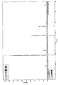
- FIG. 2 is an XRD chart of CZTS powder produced in Example 1.
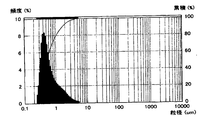
- FIG. 2 is a particle size distribution data of the powder produced in Example 1.
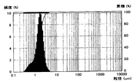
- 4 is a particle size distribution data of CZTS powder recovered by a bag filter after jet milling in Example 2.
- FIG. 3 is a particle size distribution data of CZTS powder recovered in a cyclone after jet milling in Example 2.
- FIG. It is the particle size distribution data of the CZTS powder which passed the sieve of 75 micrometers of openings while crushing the powder in Example 2.
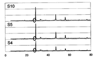
- FIG. 6 is an XRD chart of CZTS powder produced in Example 3.
- FIG. 7 is an enlarged view of a circled portion in FIG. 6. 6 is an XRD chart of CZTS powder produced in Example 4.
- FIG. 7 is an XRD chart of CZTS powder produced in Examples 5 and 6.
- FIG. 10 is an enlarged view of a circled portion in FIG. 9.
- 12 is an XRD chart of CZTS powders produced in Examples 7 to 11.
- 14 is an XRD chart of CZTS powder produced in Example 12.
- 14 is an XRD chart of CZTS powder produced in Example 13.
- 16 is an XRD chart of CZTS powder produced in Example 14.
- 16 is an XRD chart of CZTS powder produced in Example 15. It is the figure which expanded the part enclosed in FIG. 15 in a circle.
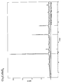
- 18 is an XRD chart of Cu 2 CoSnS 4 powder produced in Example 16.
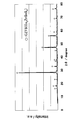
- 18 is an XRD chart of Cu 2 FeSnS 4 powder produced in Example 17.
- 19 is an XRD chart of Cu 2 MnSnS 4 powder produced in Example 18.
- the semiconductor powder according to the present invention comprises single-phase Cu-M-Sn-S (wherein M is at least one selected from Zn, Co, Ni, Fe and Mn), preferably It has a composition of Cu 2 MSnS x (wherein x is 3.5 to 4.5, desirably 4.0), and more preferably has a composition of Cu 2 ZnSnS 4 (CZTS).
- a semiconductor having such a composition has (1) abundant constituent elements so that there is no concern about supply, (2) low toxicity and environmental friendliness, and (3) a wide light absorption region and light absorption coefficient.
- the semiconductor powder of the present invention is expected to be applied as a light absorption layer of a solar cell by making it thin.
- the semiconductor powder according to the present invention is obtained by wet synthesis.
- a single-phase Cu—M—Sn—S semiconductor can be directly synthesized in a powder form simply and with high quality by wet synthesis.
- single crystal precipitation not only does it take a long time to precipitate, but in order to use it industrially, a coarse single crystal must be carefully crushed and processed into a powder with a desired particle size, although it could not be said that it was suitable for industrial use, according to wet synthesis, a powder can be directly synthesized in a relatively short time, which is suitable for industrial use.
- Identification of the semiconductor powder according to the present invention obtained by wet synthesis can be performed by XRD analysis using a powder X-ray analysis (XRD) apparatus and comparing with a single crystal chart of a JCPDS card having a corresponding composition. Confirmation that it is a single phase can be performed by confirming that the XRD chart obtained by the XRD analysis does not include an unknown peak due to a by-product other than the peak shown in the JCPDS card. The degree of crystallinity can also be estimated from the peak intensity, and the higher the peak intensity, the higher the crystallinity.
- XRD powder X-ray analysis
- the height ratio of the second peak (second highest peak) and the main peak (highest peak) in the XRD chart measured for the semiconductor powder obtained by wet synthesis is: There is a tendency to be lower than the height ratio between the second peak and the main peak in the corresponding JCPDS card, and based on this tendency, it is estimated whether or not a given semiconductor powder is obtained by wet synthesis. It is considered possible.
- each constituent particle of the semiconductor powder has a particle size in the range of 0.10 to 1000 ⁇ m, typically 0.20 to 850 ⁇ m.
- the particle size mentioned here means the diameter obtained for each particle by the particle size distribution measuring device, and does not mean the average particle size. Therefore, the semiconductor powder may have constituent particles having various sizes in the above range.
- the preferred particle size range may be appropriately determined according to the method of use and application of the semiconductor powder. For example, when a semiconductor film is formed by applying a slurry using the semiconductor powder, 0.1 to 1 ⁇ m is preferable, When the semiconductor powder is molded by pressurization or the like to make a target, 0.1 to 10 ⁇ m is preferable.
- the semiconductor powder of the present invention can be obtained as a powder form by wet synthesis, but may be appropriately pulverized using a jet mill, a ball mill or the like to give a desired particle size, or the powder thus pulverized may be a bag filter, a cyclone, etc.
- the particle size may be controlled by recovering via the.
- an aqueous solution of at least one sulfide selected from ammonium sulfide, ammonium polysulfide, sodium sulfide, thiourea and thioacetamide is prepared.
- This sulfide aqueous solution becomes a sulfur source for the semiconductor powder. It does not specifically limit as ammonium sulfide aqueous solution, What is necessary is just to use commercially available ammonium sulfide reagents, such as 1, 10, 20, 40 mass%.
- the pH of the ammonium sulfide aqueous solution is not particularly limited, and for reference, for example, the pH is 11.1 to 11.4 at a concentration of 1% by mass, and the pH is 10.0 to 10.5 at a concentration of 40% by mass. Similar to ammonium sulfide, ammonium polysulfide ((NH 4 ) 2 S x ) can also be used. Since sodium sulfide is available as a solid, the concentration may be adjusted as appropriate and used in the same concentration range as ammonium sulfide.
- the amount of the sulfide aqueous solution is selected so as to supply sulfur at a higher ratio than the sulfur content ratio in the stoichiometric composition of the semiconductor powder to be obtained.
- the composition of the semiconductor powder to be obtained is Cu 2 MSnS 4
- the Cu: M: Sn: S ratio in the preparation liquid is more than 2: 1: 1: 4, preferably 2: 1: 1: 5 or more, More preferably, by setting the ratio to 2: 1: 1: 5 to 10, a desired semiconductor powder can be obtained stably.
- inorganic acid salts include sulfates, nitrates, acetates, chlorides and combinations thereof, preferably sulfates, nitrates, acetates and combinations thereof, more preferably sulfates. It is not limited to.
- inorganic acids include sulfuric acid, nitric acid, acetic acid, hydrochloric acid and combinations thereof, preferably sulfuric acid, nitric acid, acetic acid and combinations thereof, more preferably sulfuric acid, but are not limited thereto. It is not something.
- the order of addition is preferably Sn (tin sulfate), Zn (zinc sulfate), Cu (copper sulfate), and sulfuric acid in this order.
- the reaction can be performed according to this order.
- each salt is preferably carried out in the form of an aqueous solution.
- the amount of water used for the preparation of the aqueous solution may be a minimum amount necessary for dissolving the salt in view of the solubility. That is, it is considered that there is no adverse effect due to the amount of water, and in fact, a single-phase sample can be obtained even when dissolved in an amount of water 10 times the minimum necessary amount.
- the inorganic salts of Cu, M, and Sn may be added at the same time. In that case, a solution in which three kinds of Cu, M, and Sn are dissolved is prepared, and the solution is added to the aqueous ammonium sulfide solution. That's fine.
- the addition of the inorganic acid is performed after the addition of the inorganic acid salt because the pH of the mixed solution can be easily adjusted.
- the mixed solution may be finally adjusted to pH 4-9 by adding the inorganic acid, preferably pH 5-8, more preferably Has a pH of 6.5 to 7.5. Elution of zinc on the acidic side and zinc and tin tends to be seen on the alkaline side, but within the above range, the cation does not elute and everything precipitates as a precursor, and a single-phase semiconductor after sintering A powder can be obtained.
- the mixed solution is stirred to produce a precipitate, and the mixed solution is separated into solid and liquid, and the precipitate is separated by filtration.
- Solid-liquid separation may be performed by various known methods such as natural filtration, suction filtration, and centrifugal separation, and is not particularly limited. However, since centrifugal separation may cause copper, zinc and tin to elute into the supernatant, natural filtration and suction filtration without such concerns are preferred.
- the obtained precipitate may be further subjected to repulp washing, and the amount of water at that time is not particularly limited because it is considered that there is no influence on the sample. However, it is possible to obtain a single-phase semiconductor powder without performing repulp washing.
- the precipitate separated by filtration is fired in an inert gas atmosphere or in the presence of a sulfur-containing compound excluding sulfur oxides to obtain a semiconductor powder according to the present invention. That is, the sintering may be performed in an inert gas atmosphere such as nitrogen or argon, or may be performed in the presence of a sulfur-containing compound such as hydrogen sulfide or sulfur vapor.
- a sulfur-containing compound such as hydrogen sulfide or sulfur vapor.
- the sulfur oxide SO x is excluded from the sulfur-containing compounds that can be used in the present invention because of its oxidative capacity, which adversely affects the membrane.
- the sulfur-containing compound may be a gas, but even a solid or liquid can be used by coexisting with the precipitate.
- the film can also be sulfided by putting sulfur powder together with precipitates and sintering.
- Preferred sulfur-containing compounds include hydrogen sulfide, sulfur (steam), sulfur (powder), carbon disulfide, and organic sulfur compounds.
- the sintering temperature is not particularly limited because it varies depending on the composition and atmosphere of the powder.
- 300 to 800 ° C. is preferable in terms of being easily converted to a single phase, more preferably 300 to 600 ° C., and further preferably 400 to 500 ° C. If the sintering temperature is too high, sulfur is scattered, which is not preferable.
- firing in a hydrogen sulfide atmosphere employs an atmosphere in which sulfur that should be inadequate is supplied, so firing at a high temperature is possible, so the sintering temperature may be 300 to 1000 ° C. it can.
- a step of drying the precipitate separated by filtration in an inert gas atmosphere or in the presence of a sulfur-containing compound excluding sulfur oxides may be performed prior to firing.
- air drying is not preferable because tin oxide is generated as a by-product.
- Dispersion The dispersion obtained by dispersing the semiconductor powder precursor particles in a solvent obtained as a mixture in the above production method can be used as a coating liquid for forming a thin film. That is, a semiconductor thin film can be easily formed by applying this dispersion to a substrate and baking it. Alternatively, the semiconductor powder can be obtained simply by solid-liquid separation of the dispersion and firing the filtered precipitate.
- the particle size of the precursor particles in the dispersion is not particularly limited, but is preferably 0.10 to 3.0 ⁇ m, more preferably 0.10 to 1.0 ⁇ m.
- the semiconductor powder and dispersion of the present invention are suitable for thin film formation, and can be suitably used for various applications such as a light absorption layer of a solar cell.
- the method of forming the thin film is not particularly limited, and vapor deposition by heating semiconductor powder pellets, sputtering using a semiconductor powder sintered compact target, and spin coating by applying a dispersion of semiconductor powder to a rotated substrate.
- a thin film can be easily formed based on various known methods such as dip coating by immersing the substrate in a dispersion of semiconductor powder. Accordingly, preferred forms of products produced using the semiconductor powder and dispersion of the present invention include vapor deposition pellets, sputtering targets, and semiconductor thin films.
- the dispersion used for spin coating and dip coating is not only a dispersion obtained by dispersing a semiconductor powder as a final product in a solvent, but also the above-described semiconductor powder precursor particles are dispersed in a solvent.
- the dispersion can also be used as it is.
- the semiconductor powder wet-synthesized according to the present invention contains a relatively large amount of sulfur
- the thin film already contains an amount of sulfur that is the same as or close to the stoichiometric composition at the stage before annealing.
- the sulfide is finally formed by hydrogen sulfide or sulfur annealing, metal rather than sulfide is frequently used as a raw material. It is considered that the state before the annealing is in a state of substantial sulfur deficiency.
- CZTS Cu 2 ZnSnS 4
- the particle size distribution of the obtained powder was measured with a laser diffraction / scattering particle size distribution measuring device (Microtrac MT3200 (WET), Nikkiso Co., Ltd.). The measurement conditions were such that the particle permeability was the transmission condition and the particle refractive index was 1.81. The measured data is shown in FIG.
- This semiconductor powder was subjected to XRD analysis by a powder X-ray analysis (XRD) apparatus (RINT-TTR III, Rigaku Corporation) to obtain an XRD chart shown in FIG.
- XRD powder X-ray analysis
- the peak positions of both coincide and there is no unknown peak that is, the obtained semiconductor powder has a single phase.
- CZTS Cu 2 ZnSnS 4
- the CZTS powder had a lower peak intensity around 47 ° ((220) plane) than the single crystal. This is considered that the peak near 28 ° ((112) plane) is relatively strong and oriented in the (112) plane.
- Example 2 CZTS semiconductor powder of CZTS semiconductor powder obtained in the particle size control example 1 was subjected to one of the following processes performed grain diameter control, resulting particle size distribution of the laser diffraction-scattering particle size of the powder It measured with the distribution measuring apparatus (Microtrac MT3200 (WET), Nikkiso Co., Ltd.).
- Step 1 The powder was pulverized with a jet mill (KJ-25, Kurimoto Ironworks) under conditions of a classification rotor frequency of 300 Hz and a pulverization pressure of 0.5 MPa, and recovered with a bag filter.
- Step 2 The powder was pulverized with a jet mill (KJ-25, Kurimoto Steel Works) under conditions of a classification rotor frequency of 300 Hz and a pulverization pressure of 0.5 MPa, and recovered with a cyclone.
- Step 3 A sieve having an opening of 75 ⁇ m was passed through while pulverizing the powder in a mortar.
- the particle size distribution data obtained for steps 1, 2 and 3 are shown in FIGS. 3, 4 and 5, respectively. From the results of FIGS. 2 to 5, it can be seen that the particle size distribution can be sharp or broad depending on the grinding method.
- Example 3 Preparation of CZTS semiconductor powders with different charge ratios Each raw material was prepared so that the Cu: Zn: Sn: S ratio in the charge liquid was about 2: 1: 1: 4 and about 2: 1: 1: 10. Except for changing the addition amount as appropriate, each Cu 2 ZnSnS 4 (CZTS) semiconductor powder was prepared and XRD analysis was performed in the same manner as in Example 1, and the XRD charts shown in FIGS. 6 and 7 were obtained.
- Cu: Zn: Sn: S about 2 in Example 1.
- a slightly different peak from that of the 1: 1: 5 sample appears to be due to by-product formation.
- Example 4 Preparation of CZTS semiconductor powder using different types of ammonium sulfide 1% by weight ammonium sulfide aqueous solution (colorless and transparent), 10% by weight ammonium sulfide aqueous solution (yellow), or 40 to 40% instead of 20% by weight ammonium sulfide aqueous solution
- Each Cu 2 ZnSnS 4 (in the same manner as in Example 1 except that an ammonium sulfide aqueous solution was added in an amount of 44% by mass so as to be the same as the amount of ammonium sulfide added in Example 1 in terms of sulfur.
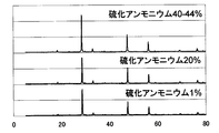
- CZTS Preparation of semiconductor powder and XRD analysis were performed to obtain an XRD chart shown in FIG. As can be seen from FIG. 8, a single-phase Cu 2 ZnSnS 4 (CZTS) semiconductor powder can be obtained regardless of the concentration or color of the aqueous ammonium sulfide solution used.
- Example 5 Production of CZTS semiconductor powder using different raw materials (1) Instead of sulfuric acid-based raw materials (tin sulfate, zinc sulfate heptahydrate, copper sulfate pentahydrate, and concentrated sulfuric acid), chloride raw materials (tin chloride, zinc chloride, copper chloride, and hydrochloric acid) are converted into Sn, In the same manner as in Example 1 except that Zn and Cu were added in an amount equivalent to the amount added in Example 1 and the pH of the feed solution was equal to the value in Example 1 (pH 7.5), Each Cu 2 ZnSnS 4 (CZTS) semiconductor powder was prepared and XRD analysis was performed, and the XRD charts shown in FIGS. 9 and 10 were obtained.
- FIG. 1 sulfuric acid-based raw materials
- chloride raw materials tin chloride, zinc chloride, copper chloride, and hydrochloric acid
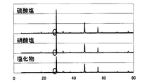
- FIGS. 9 and 10 are an enlarged view of a circled portion in FIG.
- FIGS. 9 and 10 also show an XRD chart obtained using the sulfuric acid-based material obtained in Example 1.
- the same peak behavior was observed at first glance over all diffraction angles regardless of the type of raw material.
- a peak that was attributed to tin oxide as a by-product was observed around a diffraction angle of 26.5. From these results, it can be seen that it is easier to obtain single-phase Cu 2 ZnSnS 4 (CZTS) semiconductor powder with higher quality when using a sulfuric acid-based material than when using a chloride material.
- CZTS Cu 2 ZnSnS 4
- Example 6 Production of CZTS semiconductor powder using different raw materials (2) Nitric acid raw materials (zinc nitrate, copper nitrate, and nitric acid, but tin nitrate was not available) instead of sulfuric acid raw materials (tin sulfate, zinc sulfate heptahydrate, copper sulfate pentahydrate, and concentrated sulfuric acid) (Substituted with tin sulfate) was added so as to be equivalent to the addition amount in Example 1 in terms of each element of Sn, Zn, and Cu, and the pH of the charged solution was equal to the value in Example 1 (pH 7.5) Except for this, the preparation of each Cu 2 ZnSnS 4 (CZTS) semiconductor powder and XRD analysis were carried out in the same manner as in Example 1, and the XRD charts shown in FIGS.
- Nitric acid raw materials zinc sulfate heptahydrate, copper sulfate pentahydrate, and concentrated sulfuric acid
- FIG. 10 is an enlarged view of a circled portion in FIG.
- FIGS. 9 and 10 also show an XRD chart obtained using the sulfuric acid-based material obtained in Example 1.
- the same peak behavior as when the sulfuric acid-based material was used was shown over the entire diffraction angle. From these results, it can be seen that even when a nitric acid-based material is used, single-phase Cu 2 ZnSnS 4 (CZTS) semiconductor powder can be obtained with high quality, as in the case of using a sulfuric acid-based material.
- CZTS Cu 2 ZnSnS 4
- Example 7 Production of CZTS semiconductor powder using different raw materials (3) Tin chloride (tetravalent) instead of tin sulfate, zinc nitrate instead of zinc sulfate heptahydrate, copper nitrate instead of copper sulfate pentahydrate, nitric acid instead of sulfuric acid, Sn, Zn, respectively Cu and Cu are equivalent to the addition amount in Example 1 and converted to Cu as in Example 1, except that the pH of the feed solution is equal to the value in Example 1 (pH 7.5). Production of 2 ZnSnS 4 (CZTS) semiconductor powder and XRD analysis were performed, and the XRD chart shown in FIG. 11 was obtained. For reference, FIG. 11 also shows the XRD chart obtained in Example 1.
- Tin chloride tetravalent
- Example 8 Preparation of CZTS semiconductor powder using different raw materials (4) Tin chloride (tetravalent) is substituted for tin sulfate, nitric acid is substituted for sulfuric acid, and the amount of Sn and Zn is equivalent to the amount added in Example 1, and the pH of the charged solution is the value in Example 1 (pH 7.
- a Cu 2 ZnSnS 4 (CZTS) semiconductor powder was prepared and XRD analysis was performed in the same manner as in Example 1 except that it was added so as to be equal to 5), and the XRD chart shown in FIG. 11 was obtained.
- FIG. 11 also shows the XRD chart obtained in Example 1. As is clear from FIG. 11, even when the raw material was changed as described above, a peak was observed at the same position as the sample obtained in Example 1, and as in Example 1, single-phase Cu 2 ZnSnS 4 ( It can be seen that CZTS) semiconductor powder is obtained.
- Example 9 Preparation of CZTS semiconductor powder using different raw materials (5)
- a Cu 2 ZnSnS 4 (CZTS) semiconductor powder was prepared in the same manner as in Example 1 except that tin chloride (tetravalent) was added in place of tin sulfate so as to be equivalent to the added amount in Example 1 in terms of Sn.
- Fabrication and XRD analysis were performed to obtain the XRD chart shown in FIG.
- FIG. 11 also shows the XRD chart obtained in Example 1.
- FIG. 11 even when the raw material was changed as described above, a peak was observed at the same position as the sample obtained in Example 1, and as in Example 1, single-phase Cu 2 ZnSnS 4 ( It can be seen that CZTS) semiconductor powder is obtained.
- Example 10 Production of CZTS semiconductor powder using different raw materials (6) Zinc nitrate in place of zinc sulfate heptahydrate, copper nitrate in place of copper sulfate pentahydrate, nitric acid in place of sulfuric acid, equivalent to the addition amount in Example 1 in terms of each element of Zn and Cu, respectively And a Cu 2 ZnSnS 4 (CZTS) semiconductor powder was prepared and XRD analysis was performed in the same manner as in Example 1 except that the pH of the charged solution was added so as to be equal to the value (pH 7.5) in Example 1. The XRD chart shown in FIG. 11 was obtained. For reference, FIG. 11 also shows the XRD chart obtained in Example 1. As is clear from FIG. 11, even when the raw material was changed as described above, a peak was observed at the same position as the sample obtained in Example 1, and as in Example 1, single-phase Cu 2 ZnSnS 4 ( It can be seen that CZTS) semiconductor powder is obtained.
- CZTS Cu 2 ZnS
- Example 11 Preparation of CZTS semiconductor powder using different raw materials (7) Tin chloride (divalent) instead of tin sulfate, zinc nitrate instead of zinc sulfate heptahydrate, copper nitrate instead of copper sulfate pentahydrate, nitric acid instead of sulfuric acid, Sn, Zn, respectively Cu 2 and Cu were equivalent to the amount added in Example 1 in terms of each element, and Cu 2 was added in the same manner as in Example 1 except that the pH of the charged solution was equal to the value in Example 1 (pH 7.5).
- a ZnSnS 4 (CZTS) semiconductor powder was prepared and XRD analysis was performed to obtain an XRD chart shown in FIG. For reference, FIG.
- Example 11 also shows the XRD chart obtained in Example 1. As is clear from FIG. 11, even when the raw material was changed as described above, a peak was observed at the same position as the sample obtained in Example 1, and as in Example 1, single-phase Cu 2 ZnSnS 4 ( It can be seen that CZTS) semiconductor powder is obtained.
- Example 12 Preparation of CZTS semiconductor powder with cation mixed aqueous solution
- a mixed aqueous solution prepared by dissolving 1.34 g of tin sulfate, 1.79 g of zinc sulfate heptahydrate and 3.12 g of copper sulfate pentahydrate in 200 mL of water was prepared.
- Concentrated sulfuric acid was added to the mixed solution obtained by adding this to an aqueous ammonium sulfide solution to neutralize it to obtain a charged solution having a pH of 7.5.
- the feed ratio of Cu: Zn: Sn: S in this feed liquid was approximately 2: 1: 1: 5. The mixture was stirred for 1 hour while maintaining this pH, and then centrifugal filtration was performed.
- the obtained filtrate was repulped with 200 mL of water and suction filtered.
- the precipitate thus obtained was fired (powder annealing) by holding it at 500 ° C. for 2 hours under a nitrogen atmosphere to obtain a Cu 2 ZnSnS 4 (CZTS) semiconductor powder.
- the obtained powder was subjected to XRD analysis to obtain an XRD chart shown in FIG. As is clear from FIG. 12, even when the raw materials were added almost simultaneously, a peak was observed at the same position as the sample obtained in Example 1, and as in Example 1, single-phase Cu 2 ZnSnS 4 (CZTS It can be seen that a semiconductor powder is obtained.
- Example 13 Preparation of CZTS semiconductor powder using different pH (1) Preparation of Cu 2 ZnSnS 4 (CZTS) semiconductor powder and XRD analysis were carried out in the same manner as in Example 1 except that the pH of the charged solution was set to 10.9 by not adding sulfuric acid as a neutralization step, The XRD chart shown in FIG. 13 was obtained. For reference, FIG. 13 also shows an XRD chart of the sample obtained in Example 1 prepared using a pH 7.5 feed solution. As is clear from FIG. 13, when the pH of the charged solution was 10.9, a peak that was attributed to the by-product Cu 9 S 5 was observed around a diffraction angle of 46 °. It was. Therefore, it is desirable to neutralize by adding an acid as in Example 1 to lower the pH of the charge.
- CZTS Cu 2 ZnSnS 4
- Example 14 Preparation of CZTS semiconductor powder adjusted to different pH (2)
- a Cu 2 ZnSnS 4 (CZTS) semiconductor powder was prepared in the same manner as in Example 1 except that the pH of the charged solution was changed to 5.3, 6.5, and 8.5 by changing the addition amount of sulfuric acid in the neutralization step.
- XRD analysis were performed to obtain an XRD chart shown in FIG.
- FIG. 14 also shows an XRD chart of the sample obtained in Example 1 prepared using a pH 7.5 feed solution.
- a peak is present at the same position as the sample obtained in Example 1 of the feed solution pH 7.5. It is observed that, as in Example 1, a single-phase Cu 2 ZnSnS 4 (CZTS) semiconductor powder is obtained.
- Example 15 Preparation of CZTS semiconductor powder using different drying conditions The same procedure as in Example 1 was conducted except that the precipitate obtained by natural filtration after repulp washing was dried in a nitrogen atmosphere or an air atmosphere prior to powder annealing.
- Cu 2 ZnSnS 4 (CZTS) semiconductor powder was prepared and XRD analysis was performed to obtain the XRD charts shown in FIGS.
- FIG. 16 is an enlarged view of a circled portion in FIG.
- FIGS. 15 and 16 also show an XRD chart obtained in Example 1 without a drying step. As is clear from FIG. 15, almost the same peak behavior was exhibited over all diffraction angles regardless of the drying conditions. However, from the enlarged view of FIG.
- a sample prepared through drying in an air atmosphere is a sample prepared without performing a drying process at a diffraction angle of 25 to 28 ° or dried in a nitrogen atmosphere.
- a peak behavior was observed, which appears to be due to the by-product tin oxide, which is slightly different from the sample made through the process. From these results, it is possible to obtain a single-phase Cu 2 ZnSnS 4 (CZTS) semiconductor powder with higher quality by performing the drying step in an atmosphere containing as little oxygen as possible without performing the drying step. It turns out that it is effective above.
- CZTS Cu 2 ZnSnS 4
- Example 16 Preparation of Cu 2 CoSnS 4 semiconductor powder 40 mL of an aqueous tin sulfate solution in which 1.34 g of tin sulfate was dissolved was added to 200 mL of a 1% by mass ammonium sulfide aqueous solution and stirred for 10 minutes. Next, 40 mL of an aqueous cobalt nitrate solution in which 1.82 g of cobalt nitrate hexahydrate was dissolved was added to the mixture, and the mixture was stirred for 10 minutes.
- This semiconductor powder was subjected to XRD analysis by a powder X-ray analysis (XRD) apparatus (RINT-TTR III, Rigaku Corporation) to obtain an XRD chart shown in FIG.
- XRD powder X-ray analysis
- the height ratio between the second peak and the main peak in the XRD chart was calculated to be 0.45. Therefore, in the Cu 2 CoSnS 4 single crystal powder obtained by wet synthesis, it is recognized that the height ratio between the second peak and the main peak tends to be lower than that in the JCPDS card.
- Example 17 Preparation of Cu 2 FeSnS 4 semiconductor powder 40 mL of an aqueous tin sulfate solution in which 1.34 g of tin sulfate was dissolved was added to 200 mL of a 1 mass% aqueous ammonium sulfide solution, and the mixture was stirred for 10 minutes. Next, 40 mL of an iron nitrate aqueous solution in which 2.525 g of iron nitrate nonahydrate was dissolved was added to this mixed solution, and the mixture was stirred for 10 minutes.
- This semiconductor powder was subjected to XRD analysis by a powder X-ray analysis (XRD) apparatus (RINT-TTR III, Rigaku Corporation) to obtain an XRD chart shown in FIG.
- XRD powder X-ray analysis
- the height ratio of the second peak to the main peak in the XRD chart was calculated to be 0.32. Therefore, in the Cu 2 FeSnS 4 single crystal powder obtained by wet synthesis, it is recognized that the height ratio between the second peak and the main peak tends to be lower than that in the JCPDS card.
- Example 18 Preparation of Cu 2 MnSnS 4 semiconductor powder 40 mL of an aqueous tin sulfate solution in which 1.34 g of tin sulfate was dissolved was added to 200 mL of a 1 mass% aqueous ammonium sulfide solution, and the mixture was stirred for 10 minutes. Next, 40 mL of an iron nitrate aqueous solution in which 1.81 g of manganese nitrate hexahydrate was dissolved was added to this mixed solution, and the mixture was stirred for 10 minutes.
- This semiconductor powder was subjected to XRD analysis by a powder X-ray analysis (XRD) apparatus (RINT-TTR III, Rigaku Corporation) to obtain an XRD chart shown in FIG.
- XRD powder X-ray analysis
- the height ratio between the second peak and the main peak in the XRD chart was 0.28. Therefore, it is recognized that in the Cu 2 MnSnS 4 single crystal powder obtained by wet synthesis, the height ratio between the second peak and the main peak tends to be lower than that in the JCPDS card.
- Example 19 Measurement of Seebeck coefficient in various powders Powders having various compositions shown in Table 1 were prepared. For the prepared powder, the Seebeck coefficient was measured in the same manner as in Example 1 except that the thickness of the pellet and the temperatures of the high temperature part and the low temperature part were set to the values shown in Table 1. Since the obtained Seebeck coefficients Z were all positive values, it was confirmed that all the powders having the compositions shown in Table 1 were p-type semiconductors.
Landscapes
- Chemical & Material Sciences (AREA)
- Organic Chemistry (AREA)
- Inorganic Chemistry (AREA)
- Inorganic Compounds Of Heavy Metals (AREA)
- Photovoltaic Devices (AREA)
Abstract
Description
硫化アンモニウム、多硫化アンモニウム、硫化ナトリウム、チオ尿素およびチオアセトアミドから選択される少なくとも1種の硫化物の水溶液を用意し、
該水溶液に、無機酸塩またはその水溶液の形態のCu、M、およびSnと、無機酸とを、別々または同時に添加してpH4~9の混合液とし、
該混合液を攪拌して析出物を生成させ、
該混合液を固液分離して前記析出物を濾別し、
該濾別された析出物を不活性ガス雰囲気下または硫黄酸化物を除く硫黄含有化合物の共存下で焼成して前記半導体粉末を得る
工程を含んでなる、方法が提供される。
本発明による半導体粉末は、単相のCu-M-Sn-S(式中、Mは、Zn,Co、Ni、FeおよびMnから選択される少なくとも1種である)からなり、好ましくはCu2MSnSx(式中、xは3.5~4.5であり、望ましくは4.0である)の組成を有し、より好ましくはCu2ZnSnS4(CZTS)の組成を有する。このような組成の半導体は、(1)構成元素が豊富に存在するため供給面の不安がないこと、(2)毒性が低く環境に優しいこと、(3)光吸収領域が広く且つ光吸収係数が大きいため薄膜化しても十分に光を吸収できること、(4)主としてp型の半導体特性を有し、p型からn型あるいはその逆に変化させることも可能であると考えられること、(5)バンドギャップが1.4~1.5eVにあり、バンドエンジニアリングも可能なことといった利点を有する。
特に、(4)および(5)の利点は粉体の構成元素や構成比率を変化させることで達成できるものと考えられることから、本発明で採用する湿式合成は構成元素や構成比率を容易に変えられる点で極めて有利である。そして、上記(1)~(5)の利点から、本発明の半導体粉末は薄膜化させることにより、太陽電池の光吸収層としての応用が期待される。
本発明による半導体粉末の製造方法においては、まず、硫化アンモニウム、多硫化アンモニウム、硫化ナトリウム、チオ尿素およびチオアセトアミドから選択される少なくとも1種の硫化物の水溶液を用意する。この硫化物水溶液が半導体粉末への硫黄源となる。硫化アンモニウム水溶液としては、特に限定されず、1、10、20、40質量%等といった市販の硫化アンモニウム試薬を用いればよい。硫化アンモニウム水溶液のpHも特に限定されず、参考までに示せば、例えば濃度1質量%ではpH11.1~11.4、濃度40質量%ではpH10.0~10.5である。硫化アンモニウムと同様に、多硫化アンモニウム((NH4)2Sx)も使用可能である。硫化ナトリウムは固体で入手可能であるため、濃度は適宜調整して使用すればよく、硫化アンモニウムと同じ濃度範囲で使用すればよい。
上記製造方法において混合液として得られる、半導体粉末の前駆体粒子が溶媒中に分散されてなる分散液は、それ自体、薄膜形成用のコーティング液として使用可能である。すなわち、この分散液を基材に塗布して焼成すれば半導体薄膜を簡便に形成することができる。あるいは、分散液を固液分離して、濾別した析出物を焼成するだけで、半導体粉体を簡便に得ることもできる。分散液中における前駆体粒子の粒径は特に限定されないが、好ましくは0.10~3.0μm、より好ましくは0.10~1.0μmである。
本発明の半導体粉末および分散液は、薄膜形成に適しており、それによって太陽電池の光吸収層等の種々の用途に好適に使用可能となる。薄膜形成の手法としては、特に限定されず、半導体粉末ペレットを加熱することによる蒸着、半導体粉末焼結体ターゲットを用いたスパッタリング、半導体粉末の分散液を回転させた基板に塗布することによるスピンコーティング、半導体粉末の分散液に基板を浸漬することによるディップコーティング等の公知の種々の手法に基づいて簡便に薄膜を形成することができる。したがって、本発明の半導体粉末および分散液を用いて作製される製品の好ましい形態としては、蒸着用ペレット、スパッタリングターゲット、および半導体薄膜等が挙げられる。なお、スピンコーティングおよびディップコーティングに使用される分散液としては、最終製品である半導体粉末を溶媒に分散させた分散液のみならず、上述した半導体粉末の前駆体粒子が溶媒中に分散されてなる分散液もそのまま使用することもできる。
pH=10.0の20質量%硫化アンモニウム水溶液40mlに、5.06gの硫酸錫を溶解させたpH1.1の硫酸錫水溶液22mlを添加し、15分間攪拌してpH9.8の混合液とした。次いで、この混合液に、硫酸亜鉛七水和物6.77gを溶解させたpH4.5の硫酸亜鉛水溶液14mlを添加し、15分間攪拌してpH9.6の混合液とした。更に、この混合液に、硫酸銅五水和物11.76gを溶解させたpH3.5の硫酸銅水溶液80mlを添加してpH9.3の混合液とした。こうして得られた混合液に濃硫酸2.8mlを添加して中和を行いpH7.5の仕込み液を得た。仕込み液中におけるCu:Zn:Sn:Sの仕込み比率はおよそ2:1:1:5であった。このpHを保持しながら混合液を1時間撹拌した後、自然濾過した。得られた濾過物を水750mlでリパルプ洗浄し、再度自然濾過した。こうして得られた析出物を、乾燥工程を経ることなく、窒素雰囲気下、500℃で2時間保持することにより焼成(粉末アニール)を行い、Cu2ZnSnS4(CZTS)半導体粉末を得た。得られた粉末の粒度分布をレーザー回折・散乱式粒度分布測定装置(マイクロトラックMT3200(WET)、日機装株式会社)により測定した。測定条件は粒子透過性を透過条件とし、粒子屈折率を1.81とした。測定したデータを図2に示す。
例1で得られたCZTS半導体粉末を下記のいずれかの工程に付して粒径制御を行い、得られた粉末の粒度分布をレーザー回折・散乱式粒度分布測定装置(マイクロトラックMT3200(WET)、日機装株式会社)により測定した。
工程1:粉末をジェットミル(KJ-25、栗本鐵工所)で、分級ロータ周波数300Hz、粉砕圧0.5MPaの条件で粉砕して、バグフィルタで回収した。
工程2:粉末をジェットミル(KJ-25、栗本鐵工所)で、分級ロータ周波数300Hz、粉砕圧0.5MPaの条件で粉砕して、サイクロンで回収した。
工程3:乳鉢で粉末を解砕しながら、目開き75μmの篩を通過させた。
工程1、2および3について得られた粒度分布データを図3、4および5にそれぞれ示す。図2~5の結果から、粒度分布は粉砕方法によってシャープにもブロードにもなることが分かる。
仕込み液中におけるCu:Zn:Sn:S比率が約2:1:1:4および約2:1:1:10となるように各原料の添加量を適宜変えたこと以外は例1と同様にして、各Cu2ZnSnS4(CZTS)半導体粉末の作製およびXRD分析を行い、図6および7に示されるXRDチャートを得た。図7は図6において丸く囲まれた部分を拡大した図である。なお、参考のため図6および7には例1で得られたCu:Zn:Sn:S=約2:1:1:5のサンプルで得られたXRDチャートも併せて示されている。そして、図6および7から明らかなように、仕込み比率におけるCu:Zn:Sn:S=約2:1:1:5のサンプルは、全回折角にわたって、例1のCu:Zn:Sn:S=約2:1:1:5のサンプルとほぼ同じピーク挙動を示した。これに対し、仕込み比率におけるCu:Zn:Sn:S=約2:1:1:4のサンプルは、回折角25~28°の間で、例1のCu:Zn:Sn:S=約2:1:1:5のサンプルと若干異なる、副生成物の生成に起因するとみられるピーク挙動を示した。これらの結果から、Cu:Zn:Sn:S比率が約2:1:1:5以上という、Cu2ZnSnS4の化学量論比に対して硫黄過剰の仕込み液を用いることにより単相のCu2ZnSnS4(CZTS)半導体粉末が安定して得られることが分かる。
20質量%硫化アンモニウム水溶液の代わりに、1質量%硫化アンモニウム水溶液(無色透明)、10質量%硫化アンモニウム水溶液(黄色)、または40~44質量%の硫化アンモニウム水溶液を用いて、硫化アンモニウム水溶液を硫黄換算で例1における硫化アンモニウム添加量と同量となるように添加したこと以外は例1と同様にして、各Cu2ZnSnS4(CZTS)半導体粉末の作製およびXRD分析を行い、図8に示されるXRDチャートを得た。図8から明らかなように、使用する硫化アンモニウム水溶液の濃度ないし色にかかわらず、単相のCu2ZnSnS4(CZTS)半導体粉末が得られることが分かる。
硫酸系原料(硫酸錫、硫酸亜鉛七水和物、硫酸銅五水和物、および濃硫酸)の代わりに、塩化物原料(塩化錫、塩化亜鉛、塩化銅、および塩酸)を、それぞれSn、Zn、およびCuの各元素換算で例1における添加量と等量となり且つ仕込み液のpHが例1における値(pH7.5)と等しくなるように添加したこと以外は例1と同様にして、各Cu2ZnSnS4(CZTS)半導体粉末の作製およびXRD分析を行い、図9および10に示されるXRDチャートを得た。図10は図9において丸く囲まれた部分を拡大した図である。なお、参考のため図9および10には例1で得られた硫酸系原料を用いて得られたXRDチャートも併せて示されている。そして、図9から明らかなように、原料の種類を問わず、全回折角にわたって、一見したところ同様のピーク挙動を示した。ただし、図10の拡大図から、塩化物原料を用いて作製されたサンプルは、回折角26.5の辺りに副生成物である酸化錫に起因するとみられるピークが観察された。これらの結果から、硫酸系原料を使用する方が、塩化物原料を使用するよりも、単相のCu2ZnSnS4(CZTS)半導体粉末をより高い品位で得やすいことが分かる。
硫酸系原料(硫酸錫、硫酸亜鉛七水和物、硫酸銅五水和物、および濃硫酸)の代わりに、硝酸系原料(硝酸亜鉛、硝酸銅、および硝酸、ただし硝酸錫が入手できなかったため硫酸錫で代用)を、それぞれSn、Zn、およびCuの各元素換算で例1における添加量と等量となり且つ仕込み液のpHが例1における値(pH7.5)と等しくなるように添加したこと以外は例1と同様にして、各Cu2ZnSnS4(CZTS)半導体粉末の作製およびXRD分析を行い、図9および10に示されるXRDチャートを得た。図10は図9において丸く囲まれた部分を拡大した図である。なお、参考のため図9および10には例1で得られた硫酸系原料を用いて得られたXRDチャートも併せて示されている。そして、図9および10から明らかなように、硝酸系原料を使用した場合も、全回折角にわたって、硫酸系原料を使用した場合と同様のピーク挙動を示した。これらの結果から、硝酸系原料を使用しても、硫酸系原料を使用する場合と同様に、単相のCu2ZnSnS4(CZTS)半導体粉末を高い品位で得られることが分かる。
硫酸錫の代わりに塩化錫(4価)を、硫酸亜鉛七水和物の代わりに硝酸亜鉛を、硫酸銅五水和物の代わりに硝酸銅を、硫酸の代わりに硝酸を、それぞれSn、Zn、およびCuの各元素換算で例1における添加量と等量となり且つ仕込み液のpHが例1における値(pH7.5)と等しくなるように添加したこと以外は例1と同様にして、Cu2ZnSnS4(CZTS)半導体粉末の作製およびXRD分析を行い、図11に示されるXRDチャートを得た。なお、参考のため図11には例1で得られたXRDチャートも併せて示されている。図11から明らかなように、原料を上記の通り代えた場合であっても、例1で得られたサンプルと同じ位置にピークが観察され、例1と同様、単相のCu2ZnSnS4(CZTS)半導体粉末が得られることが分かる。
硫酸錫の代わりに塩化錫(4価)を、硫酸の代わりに硝酸を、SnおよびZnの各元素換算で例1における添加量と等量となり且つ仕込み液のpHが例1における値(pH7.5)と等しくなるように添加したこと以外は例1と同様にして、Cu2ZnSnS4(CZTS)半導体粉末の作製およびXRD分析を行い、図11に示されるXRDチャートを得た。なお、参考のため図11には例1で得られたXRDチャートも併せて示されている。図11から明らかなように、原料を上記の通り代えた場合であっても、例1で得られたサンプルと同じ位置にピークが観察され、例1と同様、単相のCu2ZnSnS4(CZTS)半導体粉末が得られることが分かる。
硫酸錫の代わりに塩化錫(4価)を、Sn換算で例1における添加量と等量となるように添加したこと以外は例1と同様にして、Cu2ZnSnS4(CZTS)半導体粉末の作製およびXRD分析を行い、図11に示されるXRDチャートを得た。なお、参考のため図11には例1で得られたXRDチャートも併せて示されている。図11から明らかなように、原料を上記の通り代えた場合であっても、例1で得られたサンプルと同じ位置にピークが観察され、例1と同様、単相のCu2ZnSnS4(CZTS)半導体粉末が得られることが分かる。
硫酸亜鉛七水和物の代わりに硝酸亜鉛を、硫酸銅五水和物の代わりに硝酸銅を、硫酸の代わりに硝酸を、それぞれZnおよびCuの各元素換算で例1における添加量と等量となり且つ仕込み液のpHが例1における値(pH7.5)と等しくなるように添加したこと以外は例1と同様にして、Cu2ZnSnS4(CZTS)半導体粉末の作製およびXRD分析を行い、図11に示されるXRDチャートを得た。なお、参考のため図11には例1で得られたXRDチャートも併せて示されている。図11から明らかなように、原料を上記の通り代えた場合であっても、例1で得られたサンプルと同じ位置にピークが観察され、例1と同様、単相のCu2ZnSnS4(CZTS)半導体粉末が得られることが分かる。
硫酸錫の代わりに塩化錫(2価)を、硫酸亜鉛七水和物の代わりに硝酸亜鉛を、硫酸銅五水和物の代わりに硝酸銅を、硫酸の代わりに硝酸を、それぞれSn、ZnおよびCuの各元素換算で例1における添加量と等量となり且つ仕込み液のpHが例1における値(pH7.5)と等しくなるように添加したこと以外は例1と同様にして、Cu2ZnSnS4(CZTS)半導体粉末の作製およびXRD分析を行い、図11に示されるXRDチャートを得た。なお、参考のため図11には例1で得られたXRDチャートも併せて示されている。図11から明らかなように、原料を上記の通り代えた場合であっても、例1で得られたサンプルと同じ位置にピークが観察され、例1と同様、単相のCu2ZnSnS4(CZTS)半導体粉末が得られることが分かる。
硫酸錫1.34g、硫酸亜鉛七水和物1.79g、硫酸銅五水和物3.12gを200mLの水に溶かした混合水溶液を調製し、これを硫化アンモニウム水溶液に添加して得られた混合液に濃硫酸を添加して中和を行い、pH7.5の仕込み液を得た。この仕込み液中におけるCu:Zn:Sn:Sの仕込み比率はおよそ2:1:1:5であった。このpHを保持しながら混合液を1時間攪拌した後に、遠心ろ過を行った。得られたろ過物を水200mLでリパルプ洗浄し、吸引濾過をおこなった。こうして得られた析出物を窒素雰囲気下で500℃で2時間保持することにより焼成(粉末アニール)を行い、Cu2ZnSnS4(CZTS)半導体粉末を得た。得られた粉末についてXRD分析を行い、図12に示されるXRDチャートを得た。図12から明らかなように、原料をほぼ同時に添加した場合であっても、例1で得られたサンプルと同じ位置にピークが観察され、例1と同様、単相のCu2ZnSnS4(CZTS)半導体粉末が得られることが分かる。
中和工程である硫酸の添加を行わないことにより仕込み液のpHを10.9としたこと以外は例1と同様にして、Cu2ZnSnS4(CZTS)半導体粉末の作製およびXRD分析を行い、図13に示されるXRDチャートを得た。なお、参考のため図13にはpH7.5の仕込み液を用いて作製された例1で得られたサンプルのXRDチャートも併せて示されている。そして、図13から明らかなように、仕込み液のpHが10.9であった場合には、副生成物であるCu9S5に起因すると見られるピークが回折角46°の辺りに観察された。したがって、例1で行われているように酸を添加して中和を行い、仕込み液のpHを下げることが望ましい。
中和工程における硫酸の添加量を変えることにより仕込み液のpHを5.3、6.5、および8.5としたこと以外は例1と同様にして、Cu2ZnSnS4(CZTS)半導体粉末の作製およびXRD分析を行い、図14に示されるXRDチャートを得た。なお、参考のため図14にはpH7.5の仕込み液を用いて作製された例1で得られたサンプルのXRDチャートも併せて示されている。そして、図14から明らかなように、仕込み液pH5.3、6.5、および8.5のいずれのサンプルにおいても、仕込み液pH7.5の例1で得られたサンプルと同じ位置にピークが観察され、例1と同様、単相のCu2ZnSnS4(CZTS)半導体粉末が得られることが分かる。
リパルプ洗浄後に自然ろ過して得られた析出物を粉末アニールに先立ち窒素雰囲気下または大気雰囲気下で乾燥したこと以外は例1と同様にして、Cu2ZnSnS4(CZTS)半導体粉末の作製およびXRD分析を行い、図15および16に示されるXRDチャートを得た。図16は図15において丸く囲まれた部分を拡大した図である。なお、参考のため図15および16には例1において乾燥工程無しで得られたXRDチャートも併せて示されている。そして、図15から明らかなように、乾燥条件を問わず、全回折角にわたって、概ね同様のピーク挙動を示した。ただし、図16の拡大図から、大気雰囲気下での乾燥を経て作製されたサンプルは、回折角25~28°の間で、乾燥工程を行わないで作製されたサンプルや窒素雰囲気下での乾燥を経て作製されたサンプルとは僅かに異なる、副生成物である酸化錫に起因するとみられるピーク挙動が観察された。これらの結果から、乾燥工程を行わないか、または行うのであれば酸素を極力含まない雰囲気下で乾燥工程を行うことが、単相のCu2ZnSnS4(CZTS)半導体粉末をより高い品位で得る上で有効であることが分かる。
1質量%硫化アンモニウム水溶液200mLに1.34gの硫酸錫を溶解させた硫酸錫水溶液40mLを添加し、10分間攪拌した。次いでこの混合液に、1.82gの硝酸コバルト6水和物を溶解させた硝酸コバルト水溶液40mLを添加し、10分間攪拌した。
さらに、この混合液に3.12gの硫酸銅5水和物を溶解した硫酸銅水溶液120mLを加えて、pH11.2の混合液とした。こうして得られた混合液に濃硫酸を添加して中和を行い、pH7.5の仕込み液を得た。この仕込み液中におけるCu:Co:Sn:Sの仕込み比率はおよそ2:1:1:5であった。このpHを保持しながら混合液を1時間攪拌した後に、遠心ろ過を行った。得られたろ過物を水200mLでリパルプ洗浄し、吸引濾過をおこなった。こうして得られた析出物を窒素雰囲気下、500℃で2時間保持することにより焼成(粉末アニール)を行い、Cu2CoSnS4(CCTS)半導体粉末を得た。
1質量%硫化アンモニウム水溶液200mLに1.34gの硫酸錫を溶解させた硫酸錫水溶液40mLを添加し、10分間攪拌した。次いでこの混合液に、2.525gの硝酸鉄9水和物を溶解させた硝酸鉄水溶液40mLを添加し、10分間攪拌した。さらに、この混合液に3.12gの硫酸銅5水和物を溶解した硫酸銅水溶液120mLを加えて、pH11.2の混合液とした。こうして得られた混合液に濃硫酸を添加して中和を行い、pH7.5の仕込み液を得た。この仕込み液中におけるCu:Fe:Sn:Sの仕込み比率はおよそ2:1:1:5であった。このpHを保持しながら混合液を1時間攪拌した後に、遠心ろ過を行った。得られたろ過物を水200mLでリパルプ洗浄し、吸引濾過をおこなった。こうして得られた析出物を窒素雰囲気下、500℃で2時間保持することにより焼成(粉末アニール)を行い、Cu2FeSnS4(CITS)半導体粉末を得た。
1質量%硫化アンモニウム水溶液200mLに1.34gの硫酸錫を溶解させた硫酸錫水溶液40mLを添加し、10分間攪拌した。次いでこの混合液に、1.81gの硝酸マンガン6水和物を溶解させた硝酸鉄水溶液40mLを添加し、10分間攪拌した。さらに、この混合液に3.12gの硫酸銅5水和物を溶解した硫酸銅水溶液120mLを加えて、pH11.2の混合液とした。こうして得られた混合液に濃硫酸を添加して中和を行い、pH7.5の仕込み液を得た。この仕込み液中におけるCu:Mn:Sn:Sの仕込み比率はおよそ2:1:1:5であった。このpHを保持しながら混合液を1時間攪拌した後に、遠心ろ過を行った。得られたろ過物を水200mLでリパルプ洗浄し、吸引濾過をおこなった。こうして得られた析出物を窒素雰囲気下、500℃で2時間保持することにより焼成(粉末アニール)を行い、Cu2MnSnS4(CMTS)半導体粉末を得た。
表1に示される各種組成の粉末を用意した。用意した粉末について、ペレットの厚さならびに高温部および低温部の温度を表1に示される値としたこと以外は例1と同様にしてゼーベック係数を測定した。

Claims (11)
- 単相のCu-M-Sn-S(式中、Mは、Zn、Co、Ni、FeおよびMnから選択される少なくとも1種である)からなり、湿式合成により得られた、半導体粉末。
- Cu2MSnSx(式中、xは3.5~4.5である)の組成を有する、請求項1に記載の半導体粉末。
- Cu2ZnSnS4の組成を有する、請求項1に記載の半導体粉末。
- 前記半導体粉末の各構成粒子が0.10~1000μmの範囲内の粒径を有する、請求項1~3のいずれか一項に記載の半導体粉末。
- 単相のCu-M-Sn-S(式中、Mは、Zn、Co、Ni、FeおよびMnから選択される少なくとも1種である)からなる半導体粉末の製造方法であって、
硫化アンモニウム、多硫化アンモニウム、硫化ナトリウム、チオ尿素およびチオアセトアミドから選択される少なくとも1種の硫化物の水溶液を用意し、
該水溶液に、無機酸塩またはその水溶液の形態のCu、M、およびSnと、無機酸とを、別々または同時に添加してpH4~9の混合液とし、
該混合液を攪拌して析出物を生成させ、
該混合液を固液分離して前記析出物を濾別し、
該濾別された析出物を不活性ガス雰囲気下または硫黄酸化物を除く硫黄含有化合物の共存下で焼成して前記半導体粉末を得る
工程を含んでなる、方法。 - 得ようとする半導体粉末の化学量論組成における硫黄含有比率よりも高い比率で硫黄を供給するように前記硫化物の水溶液の量が選択される、請求項5に記載の方法。
- 前記無機酸塩が、硫酸塩、硝酸塩、酢酸塩、および塩化物からなる群から選択される少なくとも1種であり、前記無機酸が、硫酸、硝酸、酢酸、および塩酸からなる群から選択される少なくとも1種である、請求項5または6のいずれか一項に記載の方法。
- 前記焼成に先立ち、前記濾別された析出物を不活性ガス雰囲気下または硫黄酸化物を除く硫黄含有化合物の共存下で乾燥させる工程をさらに含む、請求項5~7のいずれか一項に記載の方法。
- 湿式合成により得られた、Cu-M-Sn-S(式中、Mは、Zn、Co、Ni、FeおよびMnから選択される少なくとも1種である)からなる半導体粉末の前駆体粒子が溶媒中に分散されてなる分散液。
- 請求項5に記載の析出物生成工程により得られた、請求項9に記載の分散液。
- 請求項1~4のいずれか一項に記載の半導体粉末または請求項9または10に記載の分散液を用いて作製された、蒸着用ペレット、スパッタリングターゲット、および半導体薄膜からなる群から選択される、半導体製品。
Priority Applications (2)
| Application Number | Priority Date | Filing Date | Title |
|---|---|---|---|
| US13/388,857 US20120219797A1 (en) | 2009-08-06 | 2010-06-03 | Semiconductor Powder and Method for Producing the Same |
| JP2011525824A JP5823293B2 (ja) | 2009-08-06 | 2010-06-03 | 半導体粉末およびその製造方法 |
Applications Claiming Priority (2)
| Application Number | Priority Date | Filing Date | Title |
|---|---|---|---|
| JP2009183412 | 2009-08-06 | ||
| JP2009-183412 | 2009-08-06 |
Publications (1)
| Publication Number | Publication Date |
|---|---|
| WO2011016283A1 true WO2011016283A1 (ja) | 2011-02-10 |
Family
ID=43544185
Family Applications (1)
| Application Number | Title | Priority Date | Filing Date |
|---|---|---|---|
| PCT/JP2010/059438 Ceased WO2011016283A1 (ja) | 2009-08-06 | 2010-06-03 | 半導体粉末およびその製造方法 |
Country Status (3)
| Country | Link |
|---|---|
| US (1) | US20120219797A1 (ja) |
| JP (1) | JP5823293B2 (ja) |
| WO (1) | WO2011016283A1 (ja) |
Cited By (12)
| Publication number | Priority date | Publication date | Assignee | Title |
|---|---|---|---|---|
| CN102593252A (zh) * | 2012-02-23 | 2012-07-18 | 中国科学院合肥物质科学研究院 | 一种制备铜锌锡硫薄膜太阳能电池光吸收层的方法 |
| JP2012230953A (ja) * | 2011-04-25 | 2012-11-22 | Tanaka Chemical Corp | 複合硫化物粉体及びその製造方法、化合物半導体、並びに太陽電池 |
| JP2013026541A (ja) * | 2011-07-25 | 2013-02-04 | Kyocera Corp | 半導体層の製造方法、光電変換装置の製造方法および半導体層形成用液 |
| WO2013047461A1 (ja) * | 2011-09-30 | 2013-04-04 | 凸版印刷株式会社 | 化合物半導体薄膜形成用インクおよびその製造方法 |
| WO2013099517A1 (ja) * | 2011-12-28 | 2013-07-04 | トヨタ自動車株式会社 | Czts系化合物半導体及び光電変換素子 |
| WO2013129045A1 (ja) * | 2012-02-27 | 2013-09-06 | 株式会社日本マイクロニクス | Czts系太陽電池用合金の作製方法 |
| WO2013129466A1 (ja) * | 2012-02-28 | 2013-09-06 | 京セラ株式会社 | 錯体化合物、半導体層形成用原料、半導体層の製造方法および光電変換装置の製造方法 |
| WO2013180137A1 (ja) * | 2012-05-30 | 2013-12-05 | 凸版印刷株式会社 | 化合物半導体薄膜の作製方法およびその化合物半導体薄膜を備える太陽電池 |
| JP2014506018A (ja) * | 2011-02-18 | 2014-03-06 | ユニバーシティ オブ ワシントン スルー イッツ センター フォー コマーシャリゼーション | I2−ii−iv−vi4及びi2−(ii、iv)−iv−vi4半導体フィルムを含む半導体フィルムと、前記半導体フィルムを含む電子デバイスを形成する方法 |
| US8771555B2 (en) | 2011-05-06 | 2014-07-08 | Neo Solar Power Corp. | Ink composition |
| US8828767B2 (en) | 2011-12-30 | 2014-09-09 | Industrial Technology Research Institute | Fabriation method for light absorption layer of solar cell |
| JP2018087100A (ja) * | 2016-11-28 | 2018-06-07 | 株式会社日本触媒 | 硫化物、半導体材料、及び熱電変換材料 |
Families Citing this family (9)
| Publication number | Priority date | Publication date | Assignee | Title |
|---|---|---|---|---|
| FR2949773B1 (fr) * | 2009-09-10 | 2016-01-01 | Univ Toulouse 3 Paul Sabatier | Materiau solide a l'etat divise, procede de fabrication d'un tel materiau et utilisation d'un tel materiau dans une cellule photovoltaique. |
| CN102639442A (zh) * | 2009-11-25 | 2012-08-15 | E.I.内穆尔杜邦公司 | 铜锌锡硫化物的制备 |
| FR2972443B1 (fr) * | 2011-03-09 | 2016-10-21 | Univ Paul Sabatier - Toulouse Iii (Ups) | Dispersion colloidale d'un materiau a l'etat divise forme de chalcogenure metallique dans un milieu aqueux, materiau a l'etat divise et leurs utilisations |
| JP5788832B2 (ja) * | 2011-06-06 | 2015-10-07 | トヨタ自動車株式会社 | ソルボサーマル法を用いるCu,Zn,Sn及びSを含有する硫化物系化合物半導体ナノ粒子の製造方法 |
| US20150118144A1 (en) * | 2012-05-14 | 2015-04-30 | E I Du Pont Nemours And Company | Dispersible metal chalcogenide nanoparticles |
| CN104249065B (zh) * | 2013-06-26 | 2016-12-28 | 浙江昱辉阳光能源有限公司 | 一种硅料废气吸收塔的清洗方法 |
| US10888836B2 (en) * | 2014-07-25 | 2021-01-12 | Chemical and Metal Technologies LLC | Extraction of target materials using CZTS sorbent |
| CN112614896A (zh) * | 2020-12-25 | 2021-04-06 | 广东省科学院半导体研究所 | 一种薄膜晶体管及其制备方法 |
| CN114566391A (zh) * | 2022-03-26 | 2022-05-31 | 安徽工程大学 | 一种超级电容器电极材料用过渡金属硫化物的制备方法 |
Citations (1)
| Publication number | Priority date | Publication date | Assignee | Title |
|---|---|---|---|---|
| JP2007269589A (ja) * | 2006-03-31 | 2007-10-18 | Nagaoka Univ Of Technology | 硫化物薄膜の作製方法 |
Family Cites Families (4)
| Publication number | Priority date | Publication date | Assignee | Title |
|---|---|---|---|---|
| US5051204A (en) * | 1988-11-30 | 1991-09-24 | Director-General Of Agency Of Industrial Science And Technology | Multi-element metal chalocogenide |
| WO2010138636A2 (en) * | 2009-05-26 | 2010-12-02 | Purdue Research Foundation | Synthesis of multinary chalcogenide nanoparticles comprising cu, zn, sn, s, and se |
| US7972899B2 (en) * | 2009-07-30 | 2011-07-05 | Sisom Thin Films Llc | Method for fabricating copper-containing ternary and quaternary chalcogenide thin films |
| CN102639442A (zh) * | 2009-11-25 | 2012-08-15 | E.I.内穆尔杜邦公司 | 铜锌锡硫化物的制备 |
-
2010
- 2010-06-03 US US13/388,857 patent/US20120219797A1/en not_active Abandoned
- 2010-06-03 WO PCT/JP2010/059438 patent/WO2011016283A1/ja not_active Ceased
- 2010-06-03 JP JP2011525824A patent/JP5823293B2/ja not_active Expired - Fee Related
Patent Citations (1)
| Publication number | Priority date | Publication date | Assignee | Title |
|---|---|---|---|---|
| JP2007269589A (ja) * | 2006-03-31 | 2007-10-18 | Nagaoka Univ Of Technology | 硫化物薄膜の作製方法 |
Non-Patent Citations (2)
| Title |
|---|
| C. AN ET AL: "The synthesis and characterization of nanocrystalline Cu- and Ag-based multinary sulfide semiconductors", MATERIALS RESEARCH BULLETIN, vol. 38, no. 5, 30 April 2003 (2003-04-30), pages 823 - 830, XP004424062, DOI: doi:10.1016/S0025-5408(03)00046-1 * |
| Z. GUI ET AL: "A new colloidal precursor cooperative conversion route to nanocrystalline quaternary copper sulfide", MATERIALS RESEARCH BULLETIN, vol. 39, no. 2, 2 February 2004 (2004-02-02), pages 237 - 241, XP004484873, DOI: doi:10.1016/j.materresbull.2003.09.035 * |
Cited By (21)
| Publication number | Priority date | Publication date | Assignee | Title |
|---|---|---|---|---|
| JP2014506018A (ja) * | 2011-02-18 | 2014-03-06 | ユニバーシティ オブ ワシントン スルー イッツ センター フォー コマーシャリゼーション | I2−ii−iv−vi4及びi2−(ii、iv)−iv−vi4半導体フィルムを含む半導体フィルムと、前記半導体フィルムを含む電子デバイスを形成する方法 |
| CN103650155B (zh) * | 2011-02-18 | 2016-10-12 | 华盛顿大学商业中心 | 形成包括i2-ii-iv-vi4和i2-(ii,iv)-iv-vi4半导体膜在内的半导体膜的方法以及包括所述半导体膜的电子装置 |
| CN103650155A (zh) * | 2011-02-18 | 2014-03-19 | 华盛顿大学商业中心 | 形成包括i2-ii-iv-vi4和i2-(ii,iv)-iv-vi4半导体膜在内的半导体膜的方法以及包括所述半导体膜的电子装置 |
| JP2012230953A (ja) * | 2011-04-25 | 2012-11-22 | Tanaka Chemical Corp | 複合硫化物粉体及びその製造方法、化合物半導体、並びに太陽電池 |
| US8771555B2 (en) | 2011-05-06 | 2014-07-08 | Neo Solar Power Corp. | Ink composition |
| JP2013026541A (ja) * | 2011-07-25 | 2013-02-04 | Kyocera Corp | 半導体層の製造方法、光電変換装置の製造方法および半導体層形成用液 |
| WO2013047461A1 (ja) * | 2011-09-30 | 2013-04-04 | 凸版印刷株式会社 | 化合物半導体薄膜形成用インクおよびその製造方法 |
| JPWO2013047461A1 (ja) * | 2011-09-30 | 2015-03-26 | 凸版印刷株式会社 | 化合物半導体薄膜形成用インクおよびその製造方法 |
| CN103842289A (zh) * | 2011-09-30 | 2014-06-04 | 凸版印刷株式会社 | 化合物半导体薄膜形成用油墨及其制造方法 |
| JP2013136481A (ja) * | 2011-12-28 | 2013-07-11 | Toyota Motor Corp | Czts系化合物半導体及び光電変換素子 |
| CN104039707A (zh) * | 2011-12-28 | 2014-09-10 | 丰田自动车株式会社 | Czts系化合物半导体和光电转换元件 |
| WO2013099517A1 (ja) * | 2011-12-28 | 2013-07-04 | トヨタ自動車株式会社 | Czts系化合物半導体及び光電変換素子 |
| US8828767B2 (en) | 2011-12-30 | 2014-09-09 | Industrial Technology Research Institute | Fabriation method for light absorption layer of solar cell |
| CN102593252A (zh) * | 2012-02-23 | 2012-07-18 | 中国科学院合肥物质科学研究院 | 一种制备铜锌锡硫薄膜太阳能电池光吸收层的方法 |
| WO2013129045A1 (ja) * | 2012-02-27 | 2013-09-06 | 株式会社日本マイクロニクス | Czts系太陽電池用合金の作製方法 |
| CN104245573A (zh) * | 2012-02-27 | 2014-12-24 | 日本麦可罗尼克斯股份有限公司 | Czts系太阳能电池用合金的制作方法 |
| JPWO2013129045A1 (ja) * | 2012-02-27 | 2015-07-30 | 株式会社日本マイクロニクス | Czts系太陽電池用合金の作製方法 |
| CN104245573B (zh) * | 2012-02-27 | 2016-06-08 | 日本麦可罗尼克斯股份有限公司 | Czts系太阳能电池用合金的制作方法 |
| WO2013129466A1 (ja) * | 2012-02-28 | 2013-09-06 | 京セラ株式会社 | 錯体化合物、半導体層形成用原料、半導体層の製造方法および光電変換装置の製造方法 |
| WO2013180137A1 (ja) * | 2012-05-30 | 2013-12-05 | 凸版印刷株式会社 | 化合物半導体薄膜の作製方法およびその化合物半導体薄膜を備える太陽電池 |
| JP2018087100A (ja) * | 2016-11-28 | 2018-06-07 | 株式会社日本触媒 | 硫化物、半導体材料、及び熱電変換材料 |
Also Published As
| Publication number | Publication date |
|---|---|
| JP5823293B2 (ja) | 2015-11-25 |
| JPWO2011016283A1 (ja) | 2013-01-10 |
| US20120219797A1 (en) | 2012-08-30 |
Similar Documents
| Publication | Publication Date | Title |
|---|---|---|
| JP5823293B2 (ja) | 半導体粉末およびその製造方法 | |
| Mustapha et al. | Comparative study of crystallite size using Williamson-Hall and Debye-Scherrer plots for ZnO nanoparticles | |
| Mesaros et al. | Synthesis, structural and morphological characteristics, magnetic and optical properties of Co doped ZnO nanoparticles | |
| Zaberca et al. | Surfactant-free CZTS nanoparticles as building blocks for low-cost solar cell absorbers | |
| Anbuselvan et al. | Defect related microstructure, optical and photoluminescence behaviour of Ni, Cu co-doped ZnO nanoparticles by co-precipitation method | |
| Dhanya et al. | Structural and spectroscopic characterization of bismuth-ferrites | |
| Rajesh et al. | Two-step synthesis and characterization of ZnO nanoparticles | |
| JP2002255515A (ja) | 金属酸化物微粒子の製造方法 | |
| Ramasamy et al. | Dopant induced diameter tuning of Mn-doped CdTe nanorods in aqueous solution | |
| TWI401211B (zh) | 氧化銦粉末及其製造方法 | |
| ES2687754T3 (es) | Partículas finas de titanatos de circonio y de plomo-circonio y procedimiento para su fabricación utilizando partículas de óxido de titanio hidratado | |
| Babu et al. | Surfactant assisted growth and optical studies of NiCo2O4 nanostructures through microwave heating method | |
| Du et al. | Synthesis of MgAl2O4 spinel nanoparticles via polymer-gel and isolation-medium-assisted calcination | |
| JP5588815B2 (ja) | 酸化ガリウム粉末 | |
| CN103373845A (zh) | 铟镓锌氧化物及其制法与应用 | |
| Srisombat et al. | Chemical synthesis of magnesium niobate powders | |
| Vahdati et al. | Synthesis of nano Mn-Zn ferrites by gel combustion method with three different fuels and investigation of their structure and properties | |
| Dumbrava et al. | ZINC SULFIDE FINE PARTICLES OBTAINED AT LOW TEMPERATURE. | |
| Manouchehri et al. | Facile synthesis of Co3O4/CoO nanoparticles by thermal treatment of ball-milled precursors | |
| Thang et al. | Structural, optical, ferroelectric and magnetic properties of NiTiO3 ceramic synthesized by citrate gel method | |
| CN112218841A (zh) | 氧化锌烧结体制作用氧化锌粉末和氧化锌烧结体以及它们的制造方法 | |
| Vijayaprasath et al. | Structural, optical and magnetic properties of Ni doped ZnO nanostructures prepared by co-precipitation method | |
| US4889706A (en) | Method of manufacturing fine powder of lead stannate | |
| Chaithanatkun et al. | The influence of annealing temperature on structural properties of zinc oxide nanoparticles synthesized by precipitation method | |
| Kargar et al. | Green protocol preparation of ZnO nanoparticles in Prunus cerasus juice media |
Legal Events
| Date | Code | Title | Description |
|---|---|---|---|
| 121 | Ep: the epo has been informed by wipo that ep was designated in this application |
Ref document number: 10806283 Country of ref document: EP Kind code of ref document: A1 |
|
| WWE | Wipo information: entry into national phase |
Ref document number: 2011525824 Country of ref document: JP |
|
| NENP | Non-entry into the national phase |
Ref country code: DE |
|
| WWE | Wipo information: entry into national phase |
Ref document number: 13388857 Country of ref document: US |
|
| 122 | Ep: pct application non-entry in european phase |
Ref document number: 10806283 Country of ref document: EP Kind code of ref document: A1 |