WO2011007431A1 - 撮像装置 - Google Patents
撮像装置 Download PDFInfo
- Publication number
- WO2011007431A1 WO2011007431A1 PCT/JP2009/062819 JP2009062819W WO2011007431A1 WO 2011007431 A1 WO2011007431 A1 WO 2011007431A1 JP 2009062819 W JP2009062819 W JP 2009062819W WO 2011007431 A1 WO2011007431 A1 WO 2011007431A1
- Authority
- WO
- WIPO (PCT)
- Prior art keywords
- electron emission
- emission source
- source array
- imaging device
- magnet
- Prior art date
- Legal status (The legal status is an assumption and is not a legal conclusion. Google has not performed a legal analysis and makes no representation as to the accuracy of the status listed.)
- Ceased
Links
Images





Classifications
-
- H—ELECTRICITY
- H01—ELECTRIC ELEMENTS
- H01J—ELECTRIC DISCHARGE TUBES OR DISCHARGE LAMPS
- H01J31/00—Cathode ray tubes; Electron beam tubes
- H01J31/08—Cathode ray tubes; Electron beam tubes having a screen on or from which an image or pattern is formed, picked up, converted, or stored
- H01J31/50—Image-conversion or image-amplification tubes, i.e. having optical, X-ray, or analogous input, and optical output
- H01J31/503—Image-conversion or image-amplification tubes, i.e. having optical, X-ray, or analogous input, and optical output with an electromagnetic electron-optic system
Definitions
- the present invention relates to a photoconductive type imaging device having an electron emission source array in which a plurality of electron emission sources are arranged in a plane and a photoelectric conversion film arranged to face the electron emission source array.
- the present invention relates to an imaging device using a structure.
- An electron emission source array in which a plurality of minute electron emission sources that draw electrons by applying an electric field is arranged in a matrix on a substrate plane is known as a cold cathode.
- Each of these electron emission sources can be driven at a low voltage, has a simple structure, and is being studied for application to a small imaging device using an electron emission source array.
- Patent Document 1 proposes an imaging device in which a disk-shaped permanent magnet is arranged on the back side of the imaging element, facing the imaging element, in addition to the cylindrical magnet surrounding the imaging element.
- a cylindrical magnet with a large cylinder length and cylinder diameter is used to form a magnetic field in a direction parallel to the electron emission direction in the area of the effective photoelectric conversion film that receives light. is required.
- the inventor repeated experiments to reduce the size of the imaging device, and as a result, the magnetic field strength became non-uniform when the inner diameter of the cylindrical magnet of the magnetic field focusing structure arranged around the conventional imaging device was reduced, It has been found that such downsizing is difficult.
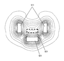
- FIG. 1 shows the execution result (strength) of the magnetic field distribution simulation when the cylindrical magnet 511 around the image sensor 821 and the disk magnet 521 on the back surface of the image sensor are used.
- the magnetic lines of force within the dotted line where the image sensor is arranged are not perpendicular to the electron emission source array but are distorted.
- the lines of magnetic force (arrows) in the region of the image sensor 821 indicated by the dotted line in the center of the figure are deviated from the vertical direction of the photoelectric conversion film.
- the present invention makes the magnetic field distribution uniform in the imaging device having the magnetic field focusing structure, and solves the problem that a uniform magnetic field cannot be obtained unless the inner diameter of the magnet is increased.
- An example is to provide an imaging device that contributes to the realization of the system.
- An imaging apparatus is arranged to face an electron emission source array with a space on the optical axis and a plurality of electron emission sources arranged in a plane perpendicular to the optical axis.
- a translucent substrate having a photoelectric conversion film, and dot-sequentially scanning the electron emission source to emit electrons to the photoelectric conversion film, and light incident from the translucent substrate on the photoelectric conversion film
- An imaging device that outputs an electrical signal corresponding to the optical image projected on the magnet, and forms a magnetic field in a direction orthogonal to each of the principal surfaces of the translucent substrate and the electron emission source array in the space;
- the light incident side on the optical axis is made of a magnetic material that is arranged with a space from the translucent substrate and connected to the magnet portion, and has an opening that defines an optical path that does not hinder the formation of the optical image.
- a magnetic field line supply unit is arranged to face an electron emission source array with a space on the optical axis and a plurality of electron emission sources arranged in
- the magnet section defines a cavity along the axis of symmetry, and is a coaxial cylinder on the optical axis that houses the translucent substrate and the electron emission source array in the center of the cavity. It can be a permanent magnet of the mold.
- the imaging device has a second magnet portion, and the second magnet portion is on the opposite side of the light incident side on the optical axis so that the axis of symmetry is coaxial with the optical axis. It may be a disc-shaped second permanent magnet that is disposed at a distance from the electron emission source array and faces the electron emission source array.
- the second permanent magnet may have an opening that is coaxial with the optical axis.
- an inner diameter of the opening of the magnetic force line supply unit is larger than an effective light receiving surface of the photoelectric conversion film on the optical axis and smaller than an inner diameter of a cavity defined in the magnet unit. can do.
- the image sensor including the photoelectric conversion film and the electron emission source array according to the present invention, and the magnet unit arranged around the image sensor for focusing the electron beam emitted from the electron emission source array.
- the imaging device to be provided by providing a magnetic force line supply portion of the magnetic body protruding to the inner diameter side of the magnet portion on the front side of the magnet portion, this also serves as a magnetic path. It is possible to improve the uniformity of the magnetic flux of the electronic travel part, reduce the leakage of magnetic flux to the front surface of the image sensor, effectively use the magnetic field, and prevent the internal reflection light from entering the photoelectric conversion film. Can be achieved.
- the plate-like magnetic force line supply unit also has a diaphragm function for preventing the internal reflection of obliquely incident light to the lens from entering the photoelectric conversion film.
- FIG. 2 is a block diagram illustrating a configuration of an electron emission source array chip including an electron emission source array and a circuit that drives the electron emission source array in the imaging device of the embodiment of the present invention, and a controller that controls the entire apparatus.
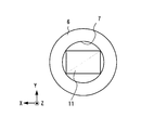
- FIG. 3 is a schematic front view showing a state where a photoelectric conversion film of the imaging element is viewed from the imaging lens system side on the optical axis when the imaging lens system is mounted on the image incident direction side in the imaging apparatus according to the embodiment of the present invention. is there.
- Electron emitting portion Aperture 6 Magnetic Field Line Supply Part 5b Second Magnet Part 7b Second Aperture 7c Aperture 9 Imaging Lens System 10 Imaging Element 11 Photoelectric Conversion Film 12 Translucent Conductive Film 13 Translucent Substrate 15 Mesh Electrode 20 Electron emission source array 22 Y scan driver 23 X scan driver 24 Electron emission source array chip 25 Support 26 Controller 30 Element substrate 31 Electron emission source 33 Lower electrode 34 Electron supply layer 35 Insulator layer 36 Upper electrode 36a Bridge part 37 Carbon Layer 77 Element isolation film 74 Gate insulating film 75 Gate electrode 72 Source electrode 76 Drain electrode 70 Interlayer insulating film 71 Contact hole 80 Expanded opening space 91 Electron emitting portion
- This imaging device includes an electron emission source array 20 in which a plurality of electron emission sources are arranged on a plane (XY plane) perpendicular to the optical axis (Z direction), and an electron emission source array 20 with a space on the optical axis.
- a light-transmitting substrate 13 having a photoelectric conversion film 11 disposed so as to be opposed to each other, scanning an electron emission source dot-sequentially to emit electrons to the photoelectric conversion film 11, and light from the light-transmitting substrate 13 This is output as an electrical signal corresponding to the optical image projected on the photoelectric conversion film 11 upon incidence.
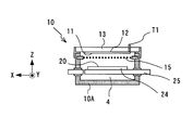
- FIG. 3 is a cross-sectional view of the cylindrical image sensor 10.
- FIG. 4 is a block diagram showing a configuration of an electron emission source array 20 of the image pickup device 10, an electron emission source array chip 24 including a Y scan driver 22 and an X scan driver 23 for driving the same, and a controller 26 for controlling the entire device. It is.
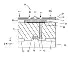
- FIG. 5 is an enlarged partial sectional view schematically showing an enlarged portion of the electron emission source 31 of the electron emission source array chip formed on the silicon element substrate 30 in order to describe the active drive type electron emission source array. is there.
- the photoelectric conversion film 11 facing the internal space of the vacuum 4 is formed on a light-transmitting conductive film 12, and the light-transmitting conductive film 12 is formed on a light-transmitting substrate 13 such as glass. Pre-formed.
- the photoelectric conversion film 11 is a light receiving unit that receives light from an object to be photographed, and is composed mainly of amorphous selenium (Se), but other materials such as silicon (Si), lead oxide, and the like.
- Compound semiconductors such as (PbO), cadmium selenide (CdSe), and gallium arsenide (GaAs) can also be used.
- substrate 13 should just be formed with the material which permeate
- transmits the light of the wavelength which the image pick-up element 10 images For example, in the case of imaging with visible light, it is made of a material such as glass that transmits visible light, and in the case of imaging with ultraviolet light, it is formed of a material such as sapphire or quartz glass that transmits ultraviolet light.
- it may be made of a material that transmits X-rays, such as beryllium (Be), silicon (Si), boron nitride (BN), aluminum oxide (Al 2 O 3 ), or the like. That's fine.
- a hole injection blocking layer such as CeO 2 for blocking hole injection from the light transmitting conductive film 12 to the photoelectric conversion film 11 is provided on the light transmitting conductive film 12 side of the photoelectric conversion film 11,
- An electron injection element layer such as Sb 2 S 3 for preventing electron injection into the photoelectric conversion film 11 can be provided on the vacuum space side.
- the mesh electrode 15 in the vacuum space is provided with a plurality of through openings and is formed of a known metal material, alloy, semiconductor material, or the like. A predetermined positive voltage is applied to the mesh electrode 15 via a connection terminal (not shown).
- the mesh electrode is an intermediate electrode provided for electron acceleration and surplus electron recovery. Thereby, the directivity of the electron beam can be improved and the resolution can be improved.
- the electron emission source array chip 24 will be described in detail later.
- the gate electrode of a MOS (Metal Oxide Semiconductor) transistor that drives the electron emission source is connected to an X scan driver (horizontal scan circuit), and the source electrode is a Y scan driver. 22 (vertical scanning circuit), and dot sequential scanning is performed.
- the Y scan driver and the X scan driver are configured as one chip integrally with the electron emission source array on the electron emission source array chip 24, and are provided on the support 25 in the glass housing 10A. Signals and voltages necessary for driving the electron emission source array chip 24 are supplied through connection terminals (not shown) provided in the glass housing 10A.
- the electron emission source array chip 24 and the translucent substrate 13 are arranged substantially in parallel with the vacuum space 4 interposed therebetween, and are vacuum-sealed in the translucent substrate 13 and the glass housing 10A sealed with frit glass or indium metal. ing.
- the electron emission source array 20 formed on the upper surface of the chip is an active drive type field emission array (FEA: Field Emitter Array) in which the electron emission source array is directly laminated on the drive circuit LSI formed on the Si wafer. It is possible to cope with high-speed driving (for example, the drive pulse width of one electron emission source 31 is several tens of ns) of the imaging operation in which dot sequential scanning is performed.
- the electron emission source array 20 includes n rows and m columns (pixels) connected to scanning lines (hereinafter referred to as scanning lines) of n lines and m lines in the Y direction (vertical direction) and the X direction (horizontal direction), respectively.
- the number is composed of a plurality of electron emission sources 31 in a matrix arrangement of n ⁇ m).
- the number of electron emission sources 31 of the electron emission source array 20 is 1920 ⁇ 1080, for example, and the size of one electron emission source 31 is 20 ⁇ 20 ⁇ m 2 .
- An electron emission portion 91 that is an opening for electron emission is provided on the surface portion of the one-electron emission source 31.
- 3 ⁇ 3 electron emission portions 91 (1 ⁇ m ⁇ ) having an electron emission source diameter of about 1 ⁇ m are formed in an 8 ⁇ 8 ⁇ m 2 region of one electron emission source 31.
- an electron current of several microamperes ( ⁇ A) is emitted from one electron emission portion 91 (emission current density is about 4 A / cm 2 ).
- ⁇ A microamperes
- the Y scanning driver 22 and the X scanning driver 23 perform dot sequential scanning and electron emission based on control signals such as a vertical synchronization signal (V-Sync), a horizontal synchronization signal (H-Sync), and a clock signal (CLK) from the controller 26.
- FIG. 5 is a diagram for explaining an electron emission source 31 in an actively driven electron emission source array and a MOS transistor for switching the electron emission source 31.
- the portion of the electron emission source 31 of the electron emission source array chip 24 (FIG. 4) is shown. It has expanded.
- the electron emission source 31 of the electron emission source array formed on the silicon element substrate 30 is formed by forming a drive circuit composed of a MOS transistor array and a Y scan driver and an X scan driver for controlling the drive circuit on the element substrate 30, It is formed on the top.
- the upper electrode 36 is connected to, for example, a Y scanning driver, and a predetermined signal is applied to each.
- the lower electrode 33 is connected to, for example, an X scanning driver, and a predetermined signal is applied to each of them in synchronization with the vertical scanning pulse. Since the intersection of the lower electrode 33 and the upper electrode 36 corresponds to the arrangement of the electron emission portions 91, in the imaging device of the embodiment, the electron emission portions 91 are sequentially driven by the lower electrode and the upper electrode 36 and approached by emitted electrons. The photoelectric conversion film region is scanned to obtain a video signal photoelectrically converted from an image formed on the photoelectric conversion film.
- the electron emission source 31 includes a lower electrode 33, an electron supply layer 34, an insulator layer 35, for example, an upper electrode 36 made of tungsten (W), and a MIS (Metal Insulator) having a laminated structure of a carbon layer 37.
- Semiconductor) type electron emission source The upper electrode 36 of the electron emission source array 20 is common to each line, and the lower electrode 33 and the electron supply layer 34 are divided to electrically separate the electron emission sources 31.
- a concave portion 91 that penetrates the insulator layer 35 and the upper electrode 36 to the electron supply layer 34 is an electron emission portion.
- an element isolation film 77 is formed in the silicon element substrate 30, and a gate insulating film 74 and a gate made of polysilicon are formed on the silicon element substrate 30 between the element isolation films 77.
- An electrode 75 is formed.
- the source electrode 72 and the drain electrode 76 are formed in a self-aligned manner by introducing impurities into the silicon element substrate 30 and activating them using the gate electrode 75 and the element isolation film 77 as a mask.
- the lower electrode 33 is electrically connected to the drain electrode 76 through a metal such as tungsten in the contact hole 71 penetrating the interlayer insulating film 70. For each lower electrode 33, an electron emission source 31 is formed separately and independently.
- An electron supply layer 34, an insulator layer 35, and an upper electrode 36 are sequentially stacked on the lower electrode 33, and an electron emission portion 91 is formed as a recess and is covered with the carbon layer 37.
- the electron emission sources 31 are separated by an enlarged opening space 80 removed by etching the electron supply layer 34.
- the electron supply layer 34 is separated and independent for each electron emission source 31 similarly to the lower electrode 33, but the bridge portion 36 a of the upper electrode 36 is installed in the space and electrically connects the adjacent electron emission sources 31. is doing.
- a carbon layer 37 is formed on the upper electrode 36 of the electron emission portion 91.
- the imaging device 10 shown in FIG. 3 when light from the outside enters the photoelectric conversion film 11 through the translucent substrate 13 and the translucent conductive film 12, the amount of incident light is increased inside the film near the translucent conductive film 12. Corresponding electron / hole pairs are generated. Of these, holes are accelerated by a strong electric field applied to the photoelectric conversion film 11 through the translucent conductive film 12 and collide with atoms constituting the photoelectric conversion film 11 one after another to generate new electron / hole pairs. . As described above, the avalanche-multiplied holes are accumulated on the side of the photoelectric conversion film 11 facing the electron emission source array 20 (the side opposite to the light-transmitting conductive film 12), and the hole pattern corresponding to the incident light image. Is formed. A current when the hole pattern and the electrons emitted from the electron emission source array 20 are combined is detected from the translucent conductive film 12 as a video signal corresponding to the incident light image.
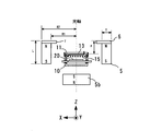
- FIG. 6 is a cross-sectional view schematically showing the configuration of the imaging element 10 and its surroundings in the imaging apparatus.
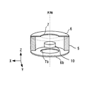
- FIG. 7 is a partially cutaway perspective view schematically showing the configuration of the imaging element 10 and its surroundings in the imaging apparatus.
- the imaging device includes a cylindrical magnet portion 5 surrounding the periphery of the imaging element 10 and an annular plate-shaped, ie, disc-shaped magnetic force line supply portion 6 fixed and connected to the magnet portion 5.
- the magnetic force line supply unit 6 is made of a magnetic material such as a soft magnetic material such as permalloy, is disposed on the light incident side on the optical axis with a space from the translucent substrate 13, and is an optical image formed on the photoelectric conversion film 11.
- An aperture 7 on the optical axis that defines an optical path that does not impede the imaging of the optical axis.
- the magnet unit 5 is a cylindrical permanent magnet that defines a cavity along the axis of symmetry and is coaxial on the optical axis that houses the translucent substrate 13 and the electron emission source array 20 in the center of the cavity.
- the imaging apparatus further includes a second magnet unit 5b, and the second magnet unit 5b emits electrons on the side opposite to the light incident side on the optical axis so that the symmetry axis is coaxial with the optical axis.
- a disk-shaped second permanent magnet is disposed at a distance from the source array 20 and faces the electron emission source array 20.
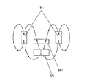
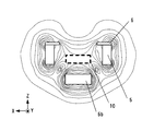
- FIG. 8 shows the execution result (strength) of the magnetic field distribution when the cylindrical magnet unit 5 around the image sensor 10 and the second disk magnet unit 5b on the back surface of the image sensor are used. Indicates. In this embodiment, it can be seen that the magnetic field strength within the dotted line where the image sensor 10 is arranged is more uniform than in the conventional case shown in FIG.
- FIG. 9 shows lines of magnetic force around the image sensor in the imaging apparatus of the embodiment shown in FIG.
- the magnet unit 5 is arranged in a direction orthogonal to the main surfaces of the translucent substrate 13 and the electron emission source array 20 in the space between the photoelectric conversion film 11 and the electron emission source array 20. It can be seen that a magnetic field is formed, that is, the magnetic field lines are oriented in the optical axis direction.
- the magnet part 5 and the 2nd magnet part 5b are arrange
- the preferable dimension range of the member of the imaging apparatus of the embodiment for obtaining the same distribution as in FIG. 8 is that the inner diameter (radius) R1 of the cylindrical magnet portion 5 is 10 to 35 mm.
- the ring outer diameter (radius) R2 is 20 to 40 mm, the ring length L of the cylindrical magnet part 5 is 15 to 25 mm, the ring thickness T of the cylindrical magnet part 5 is 5 to 10 mm, and the position of the imaging device (position of the photoelectric conversion film 11) ) P is 10 to 20 mm from the ring incident end face of the cylindrical magnet portion 5.
- the size of the image sensor is 1 ⁇ 2 inch optical (6.4 mm ⁇ 4.8 mm) to 1 inch optical (12.7 mm ⁇ 9.525 mm), and the coercive force of the magnet portion is 500 to 1500 kA / m.
- the number of inches of the image sensor size indicates the diagonal length (broken line) of the rectangular effective light receiving surface of the photoelectric conversion film 11 as shown in FIG.
- the electron beam emitted from the electron emission source array 20 in a broad manner is subjected to Lorentz force.
- the diameter of the electron beam reaching the photoelectric conversion film 11 is controlled by applying a voltage to the mesh electrode 15 disposed between the photoelectric conversion film 11 and the electron emission source array 20 and adjusting the electron velocity. Is possible.
- a plurality of focusing points can be formed by the voltage of the mesh electrode 15.
- the magnetic path (magnetic field line supply unit 6) using the soft magnetic material is arranged on the light incident side, and the magnetic field lines to be diffused are guided to the central part of the cavity, near the center.
- the magnetic field in the vicinity of the arranged image sensor 10 is made uniform so that the lines of magnetic force are perpendicular to the electron emission source array 20.
- this magnetic path (magnetic line supply unit 6) also serves as a magnetic shield that attenuates the magnetic field spreading to the outside.
- FIG. 10 shows a state in which the imaging lens system 9 is mounted on the image incident direction side of the image pickup device 10 when the image pickup apparatus is configured, that is, the lens barrel is coaxially fixed to the light incident side of the image pickup device 10. Indicates.
- the diameter of the opening 7 in the magnetic force line supply unit 6 of the soft magnetic material member is set to a size of a straight line connecting the effective area of the photoelectric conversion film 11 and the outer peripheral end of the imaging lens system 9, and antiscattering processing is performed on the inner surface.
- the surface of the ring-plate-shaped magnetic force line supply unit 6 may be subjected to light scattering prevention processing (for example, matting processing or uneven processing).
- the imaging lens system 9 is coaxial on the optical axis, and in the magnetic force line supply unit 6, the inner diameter of the opening 7 is the outer periphery of the imaging lens system.
- the opening 7 has a configuration in which the inner diameter of the opening 7 is larger than the straight line connecting the end and the effective pixel region of the photoelectric conversion film 11 or the straight line.
- the inner diameter of the opening of the magnetic force line supply unit is larger than the effective light receiving surface of the photoelectric conversion film (for example, a diagonal line) on the optical axis and smaller than the inner diameter of the cavity defined in the magnet unit. The reflection of incident light can be prevented and the sensitivity of imaging can be improved.
- the imaging device described above is made of a magnetic material that is disposed on the opposite side of the light incident side on the optical axis with a space from the electron emission source array 20 and connected to the magnet unit 5.
- a second magnetic force line supply unit 6b having the same second opening 7b as the opening 7 of the magnetic force line supply unit 6 may be provided.
- the image sensor 10 it is preferable to arrange the image sensor 10 at the center of the cylinder length of the magnet unit 5. If there is an opening edge portion of the front and rear magnetic force line supply units at a symmetric position with respect to the image sensor 10 on the optical axis, the magnetic field at the image sensor position is uniform.
- the second magnet portion 5b of the second permanent magnet can be configured to have an opening 7c that is coaxial on the optical axis. Thereby, the magnetic flux density from the 2nd magnet part 5b can be adjusted.
- the cylindrical magnet unit 5 around the image sensor 10 and the magnetic force line supply unit 6 of the magnetic shielding plate are not limited to a cylindrical shape or a disk, but are rectangular or square according to the imaging area of the image sensor 10. Even if it can be made into a cross-sectional shape and the opening is also rectangular, the same effects as in the above embodiment can be obtained.
- the imaging apparatus includes a magnetic shielding mechanism for reducing the leakage magnetic field around the imaging apparatus.
- the electron emission source array is described as a matrix arrangement of a plurality of electron emission portions in which a carbon layer is coated in a recess that penetrates the insulator layer and the upper electrode to the electron supply layer.
- the present invention is not limited to this, and can be applied to an imaging apparatus using another planar type electron emission source array such as a so-called Spindt type electron emission source matrix array.
- the structure for improving the uniformity of the magnetic flux of the electron traveling portion of the electron emission source array and preventing the leakage of the magnetic flux to the electron emission side in the present invention is a flat display device or drawing. It can be applied as a device.
Landscapes
- Physics & Mathematics (AREA)
- Electromagnetism (AREA)
- Image-Pickup Tubes, Image-Amplification Tubes, And Storage Tubes (AREA)
Abstract
Description
5 磁石部
7 開口
6 磁力線供給部
5b 第2の磁石部
7b 第2の開口
7c 開口
9 結像レンズ系
10 撮像素子
11 光電変換膜
12 透光性導電膜
13 透光性基板
15 メッシュ電極
20 電子放出源アレイ
22 Y走査ドライバ
23 X走査ドライバ
24 電子放出源アレイチップ
25 サポート
26 コントローラ
30 素子基板
31 電子放出源
33 下部電極
34 電子供給層
35 絶縁体層
36 上部電極
36a ブリッジ部
37 炭素層
77 素子分離膜
74 ゲート絶縁膜
75 ゲート電極
72 ソース電極
76 ドレイン電極
70 層間絶縁膜
71 コンタクトホール
80 拡大開口空間
91 電子放出部
図3、図4及び図5を参照して、撮像装置の撮像素子の一例を説明する。この撮像素子は、光軸(Z方向)に垂直な平面(XY平面)に複数の電子放出源が配列された電子放出源アレイ20と、光軸上に空間を隔てて電子放出源アレイ20に対向して配置された光電変換膜11を有する透光性基板13と、を含み、電子放出源を点順次走査して電子を光電変換膜11へ放出して、透光性基板13からの光入射により光電変換膜11上に投影された光学像に対応した電気信号として出力するものである。
次に、撮像装置の動作について説明する。
さらに、図12に示すように、上記の撮像装置は、光軸上の光入射側の反対側に電子放出源アレイ20から空間を隔てて配置されかつかつ磁石部5に接続された磁性体からなり、磁力線供給部6の開口7と同一の第2の開口7bを有する第2の磁力線供給部6bを設けることもできる。撮像素子前後の磁力線供給部の開口を同一とするときは、磁石部5の筒長さの中央に撮像素子10を配置することが好ましい。光軸上の撮像素子10に関して対称位置に、前後の磁力線供給部の開口縁部があれば、撮像素子位置の磁界が均等となる。
Claims (5)
- 光軸に垂直な平面に複数の電子放出源が配列された電子放出源アレイと、前記光軸上に空間を隔てて前記電子放出源アレイに対向して配置された光電変換膜を有する透光性基板と、を含み、前記電子放出源を点順次走査して電子を前記光電変換膜へ放出して、前記透光性基板からの光入射により前記光電変換膜上に投影された光学像に対応した電気信号として出力する撮像装置であって、
前記空間において前記透光性基板及び電子放出源アレイの主面それぞれに直交する方向の磁界を形成する磁石部と、
前記光軸上の光入射側に前記透光性基板から空間を隔てて配置されかつ前記磁石部に接続された磁性体からなり、前記光学像の結像を妨げない光路を画定する開口を有する磁力線供給部と、
を有することを特徴とする撮像装置。 - 前記磁石部は、その対称軸に沿った空洞を画定し、前記透光性基板及び前記電子放出源アレイを前記空洞内の中央に収納する前記光軸上に同軸の筒型の永久磁石であることを特徴とする請求項1記載の撮像装置。
- 第2の磁石部を有し、前記第2の磁石部は、その対称軸が前記光軸上に同軸となるように、前記光軸上の光入射側の反対側に前記電子放出源アレイから空間を隔てて配置されかつ、前記電子放出源アレイと対向する円盤形の第2の永久磁石であることを特徴とする請求項1又は2記載の撮像装置。
- 前記第2の永久磁石は前記光軸上に同軸となる開口を有することを特徴とする請求項3記載の撮像装置。
- 前記磁力線供給部の前記開口の内径は、前記光軸上において前記光電変換膜の有効受光面の差し渡しよりも大きくかつ前記磁石部に画定される空洞の内径より小さいことを特徴とする請求項1~4のいずれか1記載の撮像装置。
Priority Applications (3)
| Application Number | Priority Date | Filing Date | Title |
|---|---|---|---|
| US13/383,064 US20120145885A1 (en) | 2009-07-15 | 2009-07-15 | Imaging apparatus |
| JP2011522656A JP5303646B2 (ja) | 2009-07-15 | 2009-07-15 | 撮像装置 |
| PCT/JP2009/062819 WO2011007431A1 (ja) | 2009-07-15 | 2009-07-15 | 撮像装置 |
Applications Claiming Priority (1)
| Application Number | Priority Date | Filing Date | Title |
|---|---|---|---|
| PCT/JP2009/062819 WO2011007431A1 (ja) | 2009-07-15 | 2009-07-15 | 撮像装置 |
Publications (1)
| Publication Number | Publication Date |
|---|---|
| WO2011007431A1 true WO2011007431A1 (ja) | 2011-01-20 |
Family
ID=43449047
Family Applications (1)
| Application Number | Title | Priority Date | Filing Date |
|---|---|---|---|
| PCT/JP2009/062819 Ceased WO2011007431A1 (ja) | 2009-07-15 | 2009-07-15 | 撮像装置 |
Country Status (3)
| Country | Link |
|---|---|
| US (1) | US20120145885A1 (ja) |
| JP (1) | JP5303646B2 (ja) |
| WO (1) | WO2011007431A1 (ja) |
Citations (4)
| Publication number | Priority date | Publication date | Assignee | Title |
|---|---|---|---|---|
| JP2005322581A (ja) * | 2004-05-11 | 2005-11-17 | Nippon Hoso Kyokai <Nhk> | 撮像素子及びそれを用いた撮像装置 |
| JP2006134804A (ja) * | 2004-11-09 | 2006-05-25 | Nippon Hoso Kyokai <Nhk> | 撮像素子及びそれを用いた撮像装置 |
| JP2006269218A (ja) * | 2005-03-23 | 2006-10-05 | Rohm Co Ltd | 電子装置、それを利用した表示装置およびセンサ、ならびに電子装置の製造方法 |
| JP2006269217A (ja) * | 2005-03-23 | 2006-10-05 | Rohm Co Ltd | 電子装置、ならびにそれを利用した表示装置およびセンサ |
Family Cites Families (2)
| Publication number | Priority date | Publication date | Assignee | Title |
|---|---|---|---|---|
| JP2004055767A (ja) * | 2002-07-18 | 2004-02-19 | Canon Inc | 電子ビーム露光装置及び半導体デバイスの製造方法 |
| WO2011007433A1 (ja) * | 2009-07-15 | 2011-01-20 | パイオニア株式会社 | 撮像装置 |
-
2009
- 2009-07-15 US US13/383,064 patent/US20120145885A1/en not_active Abandoned
- 2009-07-15 WO PCT/JP2009/062819 patent/WO2011007431A1/ja not_active Ceased
- 2009-07-15 JP JP2011522656A patent/JP5303646B2/ja not_active Expired - Fee Related
Patent Citations (4)
| Publication number | Priority date | Publication date | Assignee | Title |
|---|---|---|---|---|
| JP2005322581A (ja) * | 2004-05-11 | 2005-11-17 | Nippon Hoso Kyokai <Nhk> | 撮像素子及びそれを用いた撮像装置 |
| JP2006134804A (ja) * | 2004-11-09 | 2006-05-25 | Nippon Hoso Kyokai <Nhk> | 撮像素子及びそれを用いた撮像装置 |
| JP2006269218A (ja) * | 2005-03-23 | 2006-10-05 | Rohm Co Ltd | 電子装置、それを利用した表示装置およびセンサ、ならびに電子装置の製造方法 |
| JP2006269217A (ja) * | 2005-03-23 | 2006-10-05 | Rohm Co Ltd | 電子装置、ならびにそれを利用した表示装置およびセンサ |
Also Published As
| Publication number | Publication date |
|---|---|
| JPWO2011007431A1 (ja) | 2012-12-20 |
| US20120145885A1 (en) | 2012-06-14 |
| JP5303646B2 (ja) | 2013-10-02 |
Similar Documents
| Publication | Publication Date | Title |
|---|---|---|
| EP0600476B1 (en) | Image pick-up apparatus and operation method of the same | |
| JP2000048743A (ja) | 平面形撮像装置及びその製造方法 | |
| JPH02304836A (ja) | 電子ビーム発生装置並びにこれを用いた陰極線管及び表示装置 | |
| US7834308B2 (en) | Imaging apparatus having electron source array that emits electrons during a blanking period | |
| JP5739763B2 (ja) | 光導電素子及び撮像デバイス | |
| JP5303646B2 (ja) | 撮像装置 | |
| JP5221761B2 (ja) | 撮像装置 | |
| JP5041875B2 (ja) | 撮像装置 | |
| JP4675578B2 (ja) | 撮像素子及びそれを用いた撮像装置 | |
| US3798453A (en) | Multichannel digital photometer | |
| JP5111276B2 (ja) | 撮像デバイス | |
| JP2002260524A (ja) | 冷陰極電子源とそれを用いて構成した撮像装置、表示装置 | |
| JP5167484B2 (ja) | 撮像装置 | |
| JP4796529B2 (ja) | 撮像装置 | |
| JP2009123423A (ja) | 撮像デバイス | |
| JPH06243777A (ja) | 冷陰極 | |
| JP2014082008A (ja) | 撮像デバイス | |
| JPH1154023A (ja) | 電子ビーム源及び電子ビーム装置 | |
| JPH04230941A (ja) | 撮像管及びその動作方法 | |
| WO2013150562A1 (ja) | 電子放出素子アレイおよびこれを備えた撮像装置 | |
| JPS63110538A (ja) | 撮像装置 | |
| JP5503387B2 (ja) | 光導電素子及び撮像デバイス | |
| JPH056749A (ja) | 撮像装置 | |
| JP2006040835A (ja) | 電子ビーム照射装置 | |
| JP2010186750A (ja) | 電子放出素子を用いた光電変換装置および撮像装置 |
Legal Events
| Date | Code | Title | Description |
|---|---|---|---|
| 121 | Ep: the epo has been informed by wipo that ep was designated in this application |
Ref document number: 09847329 Country of ref document: EP Kind code of ref document: A1 |
|
| WWE | Wipo information: entry into national phase |
Ref document number: 2011522656 Country of ref document: JP |
|
| NENP | Non-entry into the national phase |
Ref country code: DE |
|
| WWE | Wipo information: entry into national phase |
Ref document number: 13383064 Country of ref document: US |
|
| 122 | Ep: pct application non-entry in european phase |
Ref document number: 09847329 Country of ref document: EP Kind code of ref document: A1 |