WO2011004631A1 - 光電変換装置の製造方法 - Google Patents
光電変換装置の製造方法 Download PDFInfo
- Publication number
- WO2011004631A1 WO2011004631A1 PCT/JP2010/052944 JP2010052944W WO2011004631A1 WO 2011004631 A1 WO2011004631 A1 WO 2011004631A1 JP 2010052944 W JP2010052944 W JP 2010052944W WO 2011004631 A1 WO2011004631 A1 WO 2011004631A1
- Authority
- WO
- WIPO (PCT)
- Prior art keywords
- thin film
- film
- photoelectric conversion
- electrode layer
- power density
- Prior art date
- Legal status (The legal status is an assumption and is not a legal conclusion. Google has not performed a legal analysis and makes no representation as to the accuracy of the status listed.)
- Ceased
Links
Images





Classifications
-
- C—CHEMISTRY; METALLURGY
- C23—COATING METALLIC MATERIAL; COATING MATERIAL WITH METALLIC MATERIAL; CHEMICAL SURFACE TREATMENT; DIFFUSION TREATMENT OF METALLIC MATERIAL; COATING BY VACUUM EVAPORATION, BY SPUTTERING, BY ION IMPLANTATION OR BY CHEMICAL VAPOUR DEPOSITION, IN GENERAL; INHIBITING CORROSION OF METALLIC MATERIAL OR INCRUSTATION IN GENERAL
- C23C—COATING METALLIC MATERIAL; COATING MATERIAL WITH METALLIC MATERIAL; SURFACE TREATMENT OF METALLIC MATERIAL BY DIFFUSION INTO THE SURFACE, BY CHEMICAL CONVERSION OR SUBSTITUTION; COATING BY VACUUM EVAPORATION, BY SPUTTERING, BY ION IMPLANTATION OR BY CHEMICAL VAPOUR DEPOSITION, IN GENERAL
- C23C14/00—Coating by vacuum evaporation, by sputtering or by ion implantation of the coating forming material
- C23C14/06—Coating by vacuum evaporation, by sputtering or by ion implantation of the coating forming material characterised by the coating material
- C23C14/14—Metallic material, boron or silicon
- C23C14/18—Metallic material, boron or silicon on other inorganic substrates
- C23C14/185—Metallic material, boron or silicon on other inorganic substrates by cathodic sputtering
-
- H—ELECTRICITY
- H10—SEMICONDUCTOR DEVICES; ELECTRIC SOLID-STATE DEVICES NOT OTHERWISE PROVIDED FOR
- H10F—INORGANIC SEMICONDUCTOR DEVICES SENSITIVE TO INFRARED RADIATION, LIGHT, ELECTROMAGNETIC RADIATION OF SHORTER WAVELENGTH OR CORPUSCULAR RADIATION
- H10F10/00—Individual photovoltaic cells, e.g. solar cells
- H10F10/10—Individual photovoltaic cells, e.g. solar cells having potential barriers
- H10F10/17—Photovoltaic cells having only PIN junction potential barriers
- H10F10/172—Photovoltaic cells having only PIN junction potential barriers comprising multiple PIN junctions, e.g. tandem cells
-
- H—ELECTRICITY
- H10—SEMICONDUCTOR DEVICES; ELECTRIC SOLID-STATE DEVICES NOT OTHERWISE PROVIDED FOR
- H10F—INORGANIC SEMICONDUCTOR DEVICES SENSITIVE TO INFRARED RADIATION, LIGHT, ELECTROMAGNETIC RADIATION OF SHORTER WAVELENGTH OR CORPUSCULAR RADIATION
- H10F71/00—Manufacture or treatment of devices covered by this subclass
- H10F71/121—The active layers comprising only Group IV materials
-
- H—ELECTRICITY
- H10—SEMICONDUCTOR DEVICES; ELECTRIC SOLID-STATE DEVICES NOT OTHERWISE PROVIDED FOR
- H10F—INORGANIC SEMICONDUCTOR DEVICES SENSITIVE TO INFRARED RADIATION, LIGHT, ELECTROMAGNETIC RADIATION OF SHORTER WAVELENGTH OR CORPUSCULAR RADIATION
- H10F77/00—Constructional details of devices covered by this subclass
- H10F77/20—Electrodes
- H10F77/206—Electrodes for devices having potential barriers
- H10F77/211—Electrodes for devices having potential barriers for photovoltaic cells
-
- H—ELECTRICITY
- H10—SEMICONDUCTOR DEVICES; ELECTRIC SOLID-STATE DEVICES NOT OTHERWISE PROVIDED FOR
- H10F—INORGANIC SEMICONDUCTOR DEVICES SENSITIVE TO INFRARED RADIATION, LIGHT, ELECTROMAGNETIC RADIATION OF SHORTER WAVELENGTH OR CORPUSCULAR RADIATION
- H10F77/00—Constructional details of devices covered by this subclass
- H10F77/20—Electrodes
- H10F77/206—Electrodes for devices having potential barriers
- H10F77/211—Electrodes for devices having potential barriers for photovoltaic cells
- H10F77/219—Arrangements for electrodes of back-contact photovoltaic cells
-
- H—ELECTRICITY
- H10—SEMICONDUCTOR DEVICES; ELECTRIC SOLID-STATE DEVICES NOT OTHERWISE PROVIDED FOR
- H10F—INORGANIC SEMICONDUCTOR DEVICES SENSITIVE TO INFRARED RADIATION, LIGHT, ELECTROMAGNETIC RADIATION OF SHORTER WAVELENGTH OR CORPUSCULAR RADIATION
- H10F77/00—Constructional details of devices covered by this subclass
- H10F77/40—Optical elements or arrangements
- H10F77/42—Optical elements or arrangements directly associated or integrated with photovoltaic cells, e.g. light-reflecting means or light-concentrating means
- H10F77/48—Back surface reflectors [BSR]
-
- Y—GENERAL TAGGING OF NEW TECHNOLOGICAL DEVELOPMENTS; GENERAL TAGGING OF CROSS-SECTIONAL TECHNOLOGIES SPANNING OVER SEVERAL SECTIONS OF THE IPC; TECHNICAL SUBJECTS COVERED BY FORMER USPC CROSS-REFERENCE ART COLLECTIONS [XRACs] AND DIGESTS
- Y02—TECHNOLOGIES OR APPLICATIONS FOR MITIGATION OR ADAPTATION AGAINST CLIMATE CHANGE
- Y02E—REDUCTION OF GREENHOUSE GAS [GHG] EMISSIONS, RELATED TO ENERGY GENERATION, TRANSMISSION OR DISTRIBUTION
- Y02E10/00—Energy generation through renewable energy sources
- Y02E10/50—Photovoltaic [PV] energy
- Y02E10/52—PV systems with concentrators
-
- Y—GENERAL TAGGING OF NEW TECHNOLOGICAL DEVELOPMENTS; GENERAL TAGGING OF CROSS-SECTIONAL TECHNOLOGIES SPANNING OVER SEVERAL SECTIONS OF THE IPC; TECHNICAL SUBJECTS COVERED BY FORMER USPC CROSS-REFERENCE ART COLLECTIONS [XRACs] AND DIGESTS
- Y02—TECHNOLOGIES OR APPLICATIONS FOR MITIGATION OR ADAPTATION AGAINST CLIMATE CHANGE
- Y02E—REDUCTION OF GREENHOUSE GAS [GHG] EMISSIONS, RELATED TO ENERGY GENERATION, TRANSMISSION OR DISTRIBUTION
- Y02E10/00—Energy generation through renewable energy sources
- Y02E10/50—Photovoltaic [PV] energy
- Y02E10/547—Monocrystalline silicon PV cells
-
- Y—GENERAL TAGGING OF NEW TECHNOLOGICAL DEVELOPMENTS; GENERAL TAGGING OF CROSS-SECTIONAL TECHNOLOGIES SPANNING OVER SEVERAL SECTIONS OF THE IPC; TECHNICAL SUBJECTS COVERED BY FORMER USPC CROSS-REFERENCE ART COLLECTIONS [XRACs] AND DIGESTS
- Y02—TECHNOLOGIES OR APPLICATIONS FOR MITIGATION OR ADAPTATION AGAINST CLIMATE CHANGE
- Y02E—REDUCTION OF GREENHOUSE GAS [GHG] EMISSIONS, RELATED TO ENERGY GENERATION, TRANSMISSION OR DISTRIBUTION
- Y02E10/00—Energy generation through renewable energy sources
- Y02E10/50—Photovoltaic [PV] energy
- Y02E10/548—Amorphous silicon PV cells
-
- Y—GENERAL TAGGING OF NEW TECHNOLOGICAL DEVELOPMENTS; GENERAL TAGGING OF CROSS-SECTIONAL TECHNOLOGIES SPANNING OVER SEVERAL SECTIONS OF THE IPC; TECHNICAL SUBJECTS COVERED BY FORMER USPC CROSS-REFERENCE ART COLLECTIONS [XRACs] AND DIGESTS
- Y02—TECHNOLOGIES OR APPLICATIONS FOR MITIGATION OR ADAPTATION AGAINST CLIMATE CHANGE
- Y02P—CLIMATE CHANGE MITIGATION TECHNOLOGIES IN THE PRODUCTION OR PROCESSING OF GOODS
- Y02P70/00—Climate change mitigation technologies in the production process for final industrial or consumer products
- Y02P70/50—Manufacturing or production processes characterised by the final manufactured product
Definitions
- the present invention relates to a method for manufacturing a photoelectric conversion device.
- the present invention relates to a method for manufacturing a photoelectric conversion device in which a power generation layer is formed by film formation.
- a thin film solar cell in which a thin film silicon layer is stacked on a power generation layer (photoelectric conversion layer) is known.
- a thin film solar cell generally has a transparent electrode layer (first transparent electrode layer), a silicon semiconductor layer (photoelectric conversion layer), a back surface transparent electrode layer (second transparent electrode layer), a metal thin film, and a substrate. Are formed by sequentially laminating backside electrode layers including
- the back transparent electrode layer contains a metal oxide such as zinc oxide (ZnO), tin oxide (SnO 2 ), indium tin oxide (ITO) as a main component.
- a metal oxide such as zinc oxide (ZnO), tin oxide (SnO 2 ), indium tin oxide (ITO)
- ZnO zinc oxide
- SnO 2 tin oxide
- ITO indium tin oxide
- gallium oxide, aluminum oxide, fluorine or the like is added to the metal oxide.
- the integrated structure is a structure in which a plurality of power generation units are formed on a single substrate and are connected in series. The separation groove and the connection groove are formed by laser scribing in a direction perpendicular to the series connection direction.
- Patent Document 1 discloses a photoelectric conversion device including a back electrode layer including an Ag thin film.
- Patent Document 1 discloses that a Cu thin film is used for the back electrode layer in addition to the Ag thin film.
- Cu is a material having lower toughness than Ag. Therefore, the optimum range of the laser processing conditions is wider than that in the case of the Ag thin film, and high robustness against laser power fluctuations can be obtained.
- the back electrode layer including the Cu thin film can be easily optimized and controlled stably for the laser etching conditions, and can be expected to have an effect of suppressing the generation of burrs during laser processing.
- Cu is more easily oxidized than Ag, and the properties of the Cu thin film obtained by the film forming conditions and the element structure (lamination structure) are different. For this reason, even if the film forming conditions of the Ag thin film described in Patent Document 1 are applied to the Cu thin film as they are, the photoelectric conversion efficiency equivalent to that of the photoelectric conversion device including the back electrode layer including the Ag thin film cannot be obtained.
- the present invention has been made in view of such circumstances, and provides a method for manufacturing a photoelectric conversion device that is easy to perform laser etching and has high power generation efficiency.
- the present inventors paid attention to the advantages of the physical properties of Cu as described above, and intensively studied a method for manufacturing a photoelectric conversion device having high power generation efficiency even when a Cu thin film is used for the back electrode layer.
- Cu has a high light reflectance, it is easily oxidized, and when oxidized, the light reflectance also decreases.
- a photoelectric conversion apparatus since it is laminated
- a solar cell is installed outdoors and exposed to the natural environment, weather resistance is also required. Therefore, in order to obtain a photoelectric conversion device having high power generation efficiency, it is important to suppress oxidation in the Cu thin film formation process, further suppress oxidation due to aging, and ensure high light reflectivity of the Cu thin film. Become.
- the present invention provides a method for manufacturing a photoelectric conversion device including a step of forming two photoelectric conversion layers and a back electrode layer on a substrate, wherein the back electrode layer forming step includes A back transparent electrode layer forming step and a Cu thin film forming step, wherein the Cu thin film forming step includes an exhaust step and a film forming step in order, and an ultimate pressure in the exhaust step is 2 ⁇ 10 ⁇ 4 Pa or less.
- the manufacturing method of the photoelectric conversion apparatus containing that the temperature of the said film forming process is 120 degreeC or more and 240 degrees C or less is provided.
- the absorption band of the photoelectric conversion layer on the back electrode layer side is not less than 650 nm. Accordingly, the back electrode layer is required to have a high reflectivity with respect to a wavelength of 650 nm or more.
- the ultimate pressure in the exhaust process in the Cu thin film forming process is preferably 2 ⁇ 10 ⁇ 4 Pa or less. Thereby, water vapor and oxygen contained in the atmosphere are excluded to a certain concentration (500 ppm). Therefore, oxidation of the Cu thin film can be suppressed, and high light reflectance can be secured.
- the temperature of the film forming process is preferably 120 ° C. or higher and 240 ° C. or lower.
- the film forming temperature By setting the film forming temperature to 120 ° C. or higher, the high light reflectance of the Cu thin film is secured. Therefore, the short circuit current of the back electrode layer can be increased and the module output can be improved.
- the film forming temperature exceeds 240 ° C., for example, amorphous silicon p layer and n layer doping materials constituting the photoelectric conversion layer diffuse into the i layer. As a result, the open circuit voltage is lowered and the module output is reduced.
- the module output is more excellent at 150 ° C. or higher and 200 ° C. or lower.
- the film forming temperature is less than 120 ° C.
- atomic movement during Cu film formation is suppressed, and many vacancies and defects are generated at the interface with the transparent electrode layer on the back surface and the crystal grain boundary in the Cu thin film, and reflection is caused.
- the rate decreases, the short circuit current decreases, and the module output decreases.
- the film forming step includes an initial stage in which an initial target input power density is applied and a steady stage in which a steady target input power density is maintained, and the initial target input power density is 10% to 50% of the steady target input power density.
- the following is preferable.
- Cu thin film is laminated
- the energy of the sputtered Cu particles adhering to the substrate is high.
- Cu reacts with oxygen of the metal oxide that is the main component of the back surface transparent electrode layer to form a black or reddish brown Cu oxide, so that the back surface transparent electrode layer is damaged.
- the layer whose interface is oxidized becomes thick (that is, damage increases)
- the light reflectivity of the back electrode layer is significantly reduced, leading to a decrease in module efficiency.
- the initial target input power density is low.
- the initial target input power density is preferably 50% or less of the steady target input power density.
- the film forming speed becomes too slow, and the impurity gas in the atmosphere is taken into the film, so that the reflectance of the Cu thin film decreases.
- the application time of the initial target input power density is 10% to 30% of the total film forming time. If the application time of the initial target input power density exceeds 30% of the total film forming time, the tact time becomes longer and the productivity is lowered. On the other hand, if it is shorter than 10%, the initial target input power density must be increased, the damage to the interface is increased, and the reflectance is lowered.
- the film forming step includes a transition stage in which the initial target input power density transitions to a steady target input power density, and the transition time of the transition stage is 5% to 10% of the total film forming time.
- the time required for the transition stage is shorter than 5% of the total film forming time for forming the Cu film
- the Cu target in the state where the damage applied to the interface is small is terminated at a steady target input power density that gives damage before the film is formed.
- the film formation begins and oxidation proceeds.
- it exceeds 10% the tact time cannot be maintained because the design film thickness cannot be secured.
- the back electrode layer may include a protective film on the Cu thin film.
- the step of forming the protective film may be included in the Cu thin film forming step, and in that case, the protective film can be laminated on the Cu thin film without being in contact with the atmosphere.
- the protective film is for protecting the Cu thin film so as not to come into contact with, for example, water vapor or oxygen in the atmosphere. By laminating this protective film on the Cu thin film, the corrosion resistance of the Cu thin film can be improved.
- (A) shows a case where a Cu thin film is used, and (b) shows a case where an Ag thin film is used.
- FIG. 1 is a schematic diagram showing the configuration of a photoelectric conversion device manufactured by the method for manufacturing a photoelectric conversion device of the present invention.
- the photoelectric conversion device 100 is a tandem silicon solar cell, and includes a substrate 1, a transparent electrode layer 2, a first cell layer 91 (amorphous silicon) as a photoelectric conversion layer 3, and a second cell layer 92 (crystalline). Silicon-based), intermediate contact layer 5, and back electrode layer 4.
- the silicon-based is a generic name including silicon (Si), silicon carbide (SiC), and silicon germanium (SiGe).
- the crystalline silicon system means a silicon system other than the amorphous silicon system, and includes microcrystalline silicon and polycrystalline silicon.
- a method for manufacturing a photoelectric conversion device will be described by taking a process for manufacturing a solar cell panel as an example.
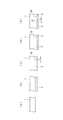
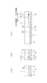
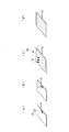
- 2 to 5 are schematic views showing a method for manufacturing the solar cell panel of the present embodiment.
- a soda float glass substrate (for example, 1.4 m ⁇ 1.1 m ⁇ plate thickness: 3.5 mm to 4.5 mm) is used as the substrate 1.
- the end face of the substrate is preferably subjected to corner chamfering or R chamfering to prevent damage due to thermal stress or impact.
- a transparent conductive film having a thickness of about 500 nm to 800 nm and having tin oxide (SnO 2 ) as a main component is formed at about 500 ° C. with a thermal CVD apparatus. At this time, a texture with appropriate irregularities is formed on the surface of the transparent conductive film.
- an alkali barrier film (not shown) may be formed between the substrate 1 and the transparent conductive film.
- a silicon oxide film (SiO 2 ) is formed at a temperature of about 500 ° C. with a thermal CVD apparatus at 50 nm to 150 nm.
- the substrate 1 is set on an XY table, and the first harmonic (1064 nm) of the YAG laser is irradiated from the film surface side of the transparent electrode film as indicated by an arrow in the figure.
- the laser power is adjusted to be appropriate for the processing speed, and the transparent electrode film is moved relative to the direction perpendicular to the series connection direction of the power generation cells so that the substrate 1 and the laser light are moved relative to each other to form the groove 10.
- a p layer, an i layer, and an n layer made of an amorphous silicon thin film are formed by a plasma CVD apparatus.
- an amorphous silicon i layer 32 and an amorphous silicon n layer 33 are formed in this order.
- the amorphous silicon p layer 31 is mainly made of amorphous B-doped silicon and has a thickness of 10 nm to 30 nm.
- the amorphous silicon i layer 32 has a thickness of 200 nm to 350 nm.
- the amorphous silicon n layer 33 is mainly P-doped silicon containing microcrystalline silicon in amorphous silicon, and has a thickness of 30 nm to 50 nm.
- a buffer layer may be provided between the amorphous silicon p layer 31 and the amorphous silicon i layer 32 in order to improve interface characteristics.
- a crystalline material as the second cell layer 92 is formed on the first cell layer 91 by a plasma CVD apparatus at a reduced pressure atmosphere: 3000 Pa or less, a substrate temperature: about 200 ° C., and a plasma generation frequency: 40 MHz or more and 100 MHz or less.
- a silicon p layer 41, a crystalline silicon i layer 42, and a crystalline silicon n layer 43 are sequentially formed.
- the crystalline silicon p layer 41 is mainly made of B-doped microcrystalline silicon and has a thickness of 10 nm to 50 nm.
- the crystalline silicon i layer 42 is mainly made of microcrystalline silicon and has a film thickness of 1.2 ⁇ m or more and 3.0 ⁇ m or less.
- the crystalline silicon n layer 43 is mainly made of P-doped microcrystalline silicon and has a thickness of 20 nm to 50 nm.
- the distance d between the plasma discharge electrode and the surface of the substrate 1 is preferably 3 mm or more and 10 mm or less. If it is smaller than 3 mm, it is difficult to keep the distance d constant from the accuracy of each component device in the film forming chamber corresponding to the large substrate, and there is a possibility that the discharge becomes unstable because it is too close. When it is larger than 10 mm, it is difficult to obtain a sufficient film forming speed (1 nm / s or more), and the uniformity of the plasma is lowered and the film quality is lowered by ion bombardment.
- An intermediate contact layer 5 serving as a semi-reflective film is provided between the first cell layer 91 and the second cell layer 92 in order to improve the contact property and obtain current matching.
- a GZO (Ga-doped ZnO) film having a thickness of 20 nm or more and 100 nm or less is formed by a sputtering apparatus using a target: Ga-doped ZnO sintered body. Further, the intermediate contact layer 5 may not be provided.
- the substrate 1 is placed on an XY table, and the second harmonic (532 nm) of the laser diode-pumped YAG laser is irradiated from the film surface side of the photoelectric conversion layer 3 as shown by the arrow in the figure.
- Pulse oscillation The laser power is adjusted so as to be appropriate for the processing speed from 10 kHz to 20 kHz, and a laser is formed so that the connection groove 11 is formed on the lateral side of the laser etching line of the transparent electrode layer 2 from about 100 ⁇ m to 150 ⁇ m. Etch. In addition, this laser may be irradiated from the substrate 1 side.
- photoelectric conversion is performed using high vapor pressure generated by energy absorbed by the amorphous silicon-based first cell layer 91 of the photoelectric conversion layer 3. Since the layer 3 can be etched, a more stable laser etching process can be performed. The position of the laser etching line is selected in consideration of positioning tolerances so as not to intersect with the etching line in the previous process.
- the back electrode layer 4 includes a back transparent electrode layer 51 and a Cu thin film 52 in order from the substrate side.
- the step of forming the back electrode layer 4 includes a back transparent electrode layer forming step and a Cu thin film forming step. Each process uses a sputtering method.
- the back transparent electrode layer 51 is formed by a sputtering apparatus.
- the back transparent electrode layer 51 is provided for the purpose of reducing contact resistance between the photoelectric conversion layer 3 and the Cu thin film 52 and improving light reflection.
- the back surface transparent electrode layer 51 is a transparent conductive film containing a metal oxide as a main component, and is, for example, a GZO (Ga-doped ZnO) film having a thickness of 50 nm to 100 nm.
- GZO Ga-doped ZnO
- the Cu thin film forming process includes an exhaust process for evacuating the chamber before forming the Cu thin film 52 and a film forming process for forming a film by applying electric power.
- the ultimate pressure in the exhaust process is set to 2 ⁇ 10 ⁇ 4 Pa or less, and then the partial pressure ratio (final pressure / Ar gas) to the ultimate pressure is 5 ⁇ .
- Ar gas is introduced so as to be 10 ⁇ 4 .
- the temperature of the film forming process is 120 ° C. or higher and 240 ° C. or lower, and a Cu thin film: film thickness of 100 nm or more and 450 nm or less is formed.
- the target input power density control profile of the film forming process maintains an initial stage in which the initial target input power density is applied, a transition stage in which the initial target input power density transitions to the steady target input power density, and a steady target input power density. It consists of a stationary stage.
- the total film forming time for forming the Cu film in the film forming process is determined by tact. Therefore, the film forming speed for reaching the target film thickness is determined. Since this film forming speed is proportional to the target input power density, the target input power density is determined in accordance with the target film forming speed. However, when the target input power density is controlled, since the initial target power is set lower than in the case where the target input power density is not controlled, the film forming speed is also reduced.
- the steady target input power density is determined.
- the initial target input power density is 10% to 50% of the steady target input power density, and is applied for a time of 10% to 30% of the total film formation time.
- the power density is changed from the initial target input power density to the steady target input power density over a period of 5% to 10% of the total film forming time.
- the initial target input power density exceeds 50% of the steady target input power density, damage to the interface between the back transparent electrode layer 51 and the Cu thin film 52 becomes large, and a high reflectance cannot be secured.
- the application time of the initial target input power density exceeds 30% of the total film forming time, or if the application time of the target input power density in the transition stage exceeds 10% of the total film forming time, the tact time cannot be maintained.
- a protective film may be formed on the Cu thin film 52 without being exposed to the atmosphere in the same chamber.
- the protective film uses Ti having a high anticorrosion effect against Cu.
- the thickness of the protective film is 5 nm or more and 150 nm or less.
- Other examples of highly anticorrosive films include metal oxide films such as Cr-O. However, since they are oxides, when they are formed in the same chamber, oxygen is released into the atmosphere, which causes oxidation of the Cu thin film. become. In addition, the cost increases if a separate chamber is used.
- the metal, Cr, Al, or Ti is used. Of these, Ti has the strongest anticorrosion effect because it produces a dense TiO 2 non-passive film. Cr and Al are alloyed with Cu to lower the reflection characteristics. If the film thickness is thinner than 5 nm, the desired anticorrosive effect cannot be obtained. If it is thicker than 150 nm, peeling due to stress tends to occur.
- FIG. 3 (c) and FIG. 4 (a) The power generation region is divided, and the film edge around the substrate edge is laser-etched to eliminate the effect of short circuit at the serial connection portion.
- the substrate 1 is set on an XY table, and the second harmonic (532 nm) of the laser diode pumped YAG laser is irradiated from the substrate 1 side.
- the laser light is absorbed by the transparent electrode layer 2 and the photoelectric conversion layer 3, and the back electrode layer 4 explodes using the high gas vapor pressure generated at this time, and the back electrode layer 4 / photoelectric conversion layer 3 / transparent electrode layer 2 is removed.
- Pulse oscillation 1 kHz or more and 100 kHz or less, the laser power is adjusted so as to be suitable for the processing speed, and the position of 5 mm to 20 mm from the end of the substrate 1 is insulated in the X direction as shown in FIG. Laser etching is performed so as to form the groove 15.
- 3C is a cross-sectional view in the X direction in which the photoelectric conversion layer 3 is cut in the direction in which the photoelectric conversion layer 3 is connected in series. A state (see FIG. 4A) where the conversion layer 3 / transparent electrode layer 2 has been removed by polishing should be present (see FIG.
- the insulating groove formed to represent the Y-direction cross section at this position will be described as the X-direction insulating groove 15.
- the Y-direction insulating groove does not need to be provided because the film surface polishing removal processing of the peripheral film removal region of the substrate 1 is performed in a later process.
- the insulating groove 15 exhibits an effective effect in suppressing external moisture intrusion into the solar cell module 6 from the end portion of the solar cell panel by terminating the etching at a position of 5 mm to 15 mm from the end of the substrate 1. Therefore, it is preferable.
- the laser beam in the above steps is a YAG laser
- those that can be used similarly such as a YVO4 laser and a fiber laser.
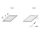
- FIG. 4 (a: view from the solar cell film side, b: view from the substrate side of the light receiving surface) Since the laminated film around the substrate 1 (peripheral film removal region 14) has a step and is easy to peel off in order to ensure a sound adhesion / seal surface with the back sheet 24 via EVA or the like in a later process, The film is removed to form a peripheral film removal region 14. In removing the film over the entire circumference of the substrate 1 at 5 to 20 mm from the end of the substrate 1, the X direction is closer to the substrate end than the insulating groove 15 provided in the step (c) of FIG. 3, and the Y direction is the substrate.
- the back electrode layer 4 / photoelectric conversion layer 3 / transparent electrode layer 2 are removed by using grinding stone polishing, blast polishing or the like on the substrate end side with respect to the groove 10 near the end side portion. Polishing debris and abrasive grains were removed by cleaning the substrate 1.
- FIG. 10 The attachment portion of the terminal box 23 is provided with an opening through window in the back sheet 24 and takes out the current collector plate. Insulating materials are provided in a plurality of layers in the opening through window portion to suppress intrusion of moisture and the like from the outside. Current is collected from the photovoltaic power generation cells at one end and the photovoltaic power generation cells at the other end in series using Cu foil so that power can be taken out from the terminal box 23 on the back side of the solar panel. To process. Cu foil arranges an insulating sheet wider than Cu foil width in order to prevent a short circuit with each part.
- an adhesive filler sheet made of EVA (ethylene vinyl acetate copolymer) or the like is disposed so as to cover the entire solar cell module 6 and not protrude from the substrate 1. .
- a back sheet 24 having a high waterproof effect is installed on the EVA.
- the back sheet 24 has a three-layer structure of PET sheet / Al foil / PET sheet so that the waterproof and moisture-proof effect is high.
- the EVA sheet is placed in a predetermined position until the back sheet 24 is deaerated in a reduced pressure atmosphere by a laminator and pressed at about 150 ° C. to 160 ° C., and EVA is crosslinked and brought into close contact.
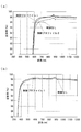
- FIG. 6 shows the wavelength dispersion of the light reflectance of the metal thin film when the ultimate pressure in the exhaust process is changed.
- (A) is a Cu thin film and (b) is an Ag thin film.
- the horizontal axis represents wavelength and the vertical axis represents reflectance.
- the Ag thin film secured a high reflectance at any ultimate pressure.
- the reflectance of the Cu thin film decreased when the ultimate pressure was higher than 2 ⁇ 10 ⁇ 4 Pa. Since Cu is more easily oxidized than Ag, it is necessary to set a suitable ultimate vacuum. In order to suppress oxidation of the Cu thin film, it is preferable that the ultimate pressure / Ar gas partial pressure ratio is 5 ⁇ 10 ⁇ 4 or less. By doing so, the quantity of water vapor
- both the Cu thin film and the Ag thin film had stable reflectance at a wavelength of 650 nm or more.
- the wavelength reaching the back electrode layer is 650 nm or more, it was confirmed that the Cu thin film can be applied to the tandem solar cell.
- Film forming temperature A 200-nm-thick Cu thin film was formed on a glass substrate to prepare a test piece. Film formation was performed by using a sputtering apparatus, exhausting the ultimate pressure to 2 ⁇ 10 ⁇ 4 Pa or less, introducing Ar gas as a sputtering gas, and generating discharge. At this time, the film forming temperatures were 100 ° C., 110 ° C., 120 ° C., 170 ° C., 240 ° C., and 250 ° C., respectively. Other film forming conditions were common to each test piece. The reflectance of each test piece prepared above was measured.
- FIG. 7 shows the wavelength dispersion of the reflectance depending on the film forming temperature when a 200 nm-thick Cu thin film is formed.
- the horizontal axis represents wavelength and the vertical axis represents reflectance.
- a Cu thin film having a reflectivity of 97% or more could be formed when the film forming temperature was 120 ° C. or higher.
- the transparent electrode layer was SnO 2 having a thickness of 500 nm to 800 nm.
- the p layer has a thickness of 10 nm to 30 nm
- the i layer has a thickness of 200 nm to 350 nm
- the n layer has a thickness of 30 nm to 50 nm.
- the intermediate contact layer was a GZO film having a thickness of 20 nm to 100 nm.
- the thickness of the p layer was 10 nm to 50 nm
- the thickness of the i layer was 1.2 ⁇ m to 3.0 ⁇ m
- the thickness of the n layer was 20 nm to 50 nm.
- the back transparent electrode layer was a GZO film having a thickness of 50 nm to 100 nm.
- the protective film was a Ti film having a thickness of 5 nm to 150 nm.
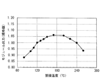
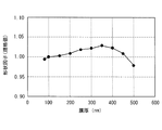
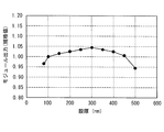
- FIGS. 8 to 11 show the short-circuit current, open-circuit voltage, form factor, and module output of the tandem solar cell module when the film forming temperature is changed from 80 ° C. to 260 ° C. in the Cu thin film forming step.
- the horizontal axis represents the film forming temperature
- the vertical axis represents the short circuit current, the open circuit voltage, the form factor, and the standard value of the module output.
- the film forming temperature was less than 120 ° C.
- the short circuit current was remarkably lowered, and the module output was lowered.
- the movement of atoms during Cu film formation is suppressed, many vacancies and defects are generated at the interface with the back transparent electrode layer and the crystal grain boundary in the Cu thin film, and the reflectivity is greatly reduced. Conceivable.
- excellent module efficiency can be obtained when the film forming temperature is 120 ° C. or higher and 240 ° C. or lower. Since the module output is maximized when the temperature is 150 ° C. to 200 ° C., the module efficiency is more excellent when the temperature is preferably 150 ° C. or more and 200 ° C. or less.
- FIG. 12 illustrates a control profile of target input power density in the film forming process in the process of forming the Cu thin film.
- the horizontal axis represents the film forming time (standard value)
- the vertical axis represents the target input power density (standard value).
- the control profile includes an initial stage for applying the initial target input power density, a transition stage for transitioning from the initial target input power density to the steady target input power density, and a steady stage for maintaining the steady target input power density.
- the initial target input power density in the initial stage is set to 20% of the steady target input power density, and power is applied over 20% of the total film forming time.
- the film is formed by increasing the initial target input power density from the initial target input power density over 10% of the total film formation time.
- the initial target input power density in the initial stage is set to 40% of the steady target input power density, and power is applied over 10% of the total film forming time.
- the film is formed by increasing the initial target input power density from the initial target input power density over 10% of the total film formation time. It should be noted that film formation at a constant target input power density from the start of film formation to the end of film formation is defined as “no control”.
- FIG. 13 shows the wavelength dispersion of the light reflectance of the Cu thin film with and without target input power density control during metal thin film formation.
- (A) is a Cu thin film
- (b) is an Ag thin film.
- the horizontal axis represents wavelength and the vertical axis represents reflectance.
- the reflectance decreased unless the target input power density was controlled. Since Cu is easier to oxidize than Ag, it was confirmed that control of target input power density is required to suppress oxidation.
- the control profile 1 was able to secure a higher light reflectance than the control profile 2. This is because in the initial stage of the film forming process, the target input power density was lowered and the application time was lengthened, so that damage to the interface between the back transparent electrode layer and the Cu thin film was reduced, and oxidation was suppressed. is there.
- the Cu thin film is easily oxidized at the interface. According to the above results, the Cu thin film is oxidized at the interface. Can be suppressed.
- FIG. 14 shows the wavelength dispersion of the reflectance of light when the film thickness of the Cu thin film is changed.
- the horizontal axis represents wavelength and the vertical axis represents reflectance.
- the module configuration was the same as when the film formation temperature was examined above.
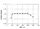
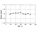
- 15 to 18 show the short-circuit current, open-circuit voltage, form factor, and module output of the tandem solar cell module when the thickness of the Cu thin film is changed.
- the horizontal axis represents the film thickness of the Cu thin film
- the vertical axis represents the standard values of the short circuit current, the open circuit voltage, the form factor, and the module output. Increasing the thickness of the Cu thin film increased the short circuit current and the open circuit voltage, and improved the module output and the shape factor.
- the film thickness of the Cu thin film exceeds 450 nm, the processing accuracy by laser etching is lowered, so that the shape factor is lowered. According to the above results, excellent module efficiency is obtained when the thickness of the Cu thin film is 100 nm or more and 450 nm or less.
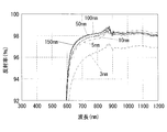
- FIG. 19 shows the wavelength dispersion of the light reflectance of the Cu thin film / Ti film when a test piece with a different thickness of the Ti film is heat-treated in the atmosphere at 200 ° C.
- a Ti film is used as a protective film for preventing corrosion of the Cu thin film, and the film thickness of the Ti film is set to 5 nm or more and 150 nm or less to ensure high reflectivity of the Cu thin film without peeling. Can do.
Landscapes
- Chemical & Material Sciences (AREA)
- Inorganic Chemistry (AREA)
- Chemical Kinetics & Catalysis (AREA)
- Engineering & Computer Science (AREA)
- Materials Engineering (AREA)
- Mechanical Engineering (AREA)
- Metallurgy (AREA)
- Organic Chemistry (AREA)
- Photovoltaic Devices (AREA)
- Physical Vapour Deposition (AREA)
Abstract
レーザーエッチングが容易であり、且つ、高い発電効率を有する光電変換装置の製造方法を提供する。基板(1)上に、2つの光電変換層(3)と、裏面電極層(4)とを形成する工程を含む光電変換装置(100)の製造方法であって、該光電変換装置(100)の製造方法は、前記裏面電極層形成工程が裏面透明電極層形成工程と、Cu薄膜形成工程とを備え、前記Cu薄膜形成工程が、順に排気工程と製膜工程とを含み、前記排気工程の到達圧力が、2×10⁻⁴Pa以下であって、前記製膜工程の温度が、120℃以上240℃以下であることを含む。
Description
本発明は、光電変換装置の製造方法に関する。特に、発電層を製膜で作製する光電変換装置の製造方法に関する。
光を受光して電力に変換する光電変換装置として、例えば発電層(光電変換層)に薄膜シリコン系の層を積層させた薄膜系太陽電池が知られている。薄膜系太陽電池は、一般に、基板上に、透明電極層(第1透明電極層)、シリコン系半導体層(光電変換層)、及び、裏面透明電極層(第2透明電極層)と金属薄膜とを含む裏面電極層を順次積層して構成される。
裏面透明電極層は、酸化亜鉛(ZnO)、酸化スズ(SnO2)、酸化インジウム錫(ITO)などの金属酸化物が主成分とされる。裏面透明電極層を低抵抗とするために、上記金属酸化物に酸化ガリウムや酸化アルミニウム、フッ素などが添加される。しかし、裏面透明電極層は金属電極と比較して高抵抗であるため、光電変換層で発生した電流が裏面透明電極層を流れる間に電力損失が生じる。そこで、外部へ取り出せる電力を増加させるために、損失を小さくする集積構造が知られている。集積構造とは、発電ユニットを1枚の基板上に複数個形成し、それぞれを直列接続したものである。分離溝や接続溝は、直列接続方向に対して垂直方向にレーザスクライブすることによって形成される。
集積型太陽電池の発電性能を向上させるためには、金属薄膜の反射率向上と裏面電極層の低抵抗化が重要である。このため、特に薄膜シリコン系太陽電池や薄膜シリコン系タンデム型太陽電池の金属薄膜には、一般に、広範囲の波長で高い反射率を示すAg薄膜が用いられている。特許文献1に、Ag薄膜を含む裏面電極層を備える光電変換装置が開示されている。
しかし、Agは高い靭性を有するため、裏面電極層をレーザーエッチングした際にバリが発生し易くなる。従って、レーザーエッチングの条件を最適化して安定制御する必要が生じる。しかし、Ag薄膜はレーザー加工条件の最適範囲が狭く、ロバスト性も低いため、制御が難しい。特許文献1では、Ag薄膜以外にCu薄膜を裏面電極層に用いることを開示している。CuはAgよりも靭性の低い材料である。そのため、レーザー加工条件の最適範囲がAg薄膜の場合よりも広がり、レーザーパワー変動などに対し高いロバスト性が得られる。この結果、Cu薄膜を備える裏面電極層は、レーザーエッチング条件の最適化及び安定制御が容易となり、レーザー加工時におけるバリの発生を抑制する効果が期待できる。一方で、CuはAgよりも酸化されやすく、製膜条件や素子構造(積層構成)により得られるCu薄膜の物性は異なる。このため、特許文献1に記載のAg薄膜の製膜条件をそのままCu薄膜へ適用しても、Ag薄膜を含む裏面電極層を備えた光電変換装置と同等の光電変換効率は得られなかった。
本発明は、このような事情に鑑みてなされたものであって、レーザーエッチングが容易であり、且つ、高い発電効率を有する光電変換装置の製造方法を提供する。
本発明者らは、上述のようなCuの物性の利点に着目し、Cu薄膜を裏面電極層に用いた場合でも、高い発電効率を有する光電変換装置の製造方法について鋭意検討した。Cuは高い光反射率を有するが、酸化されやすく、酸化されると光の反射率も低下する。また、光電変換装置に応用した際、金属酸化物を主成分とする裏面透明電極層上に積層されるため、さらに酸化されやすい条件となる。また、太陽電池は屋外に設置され自然環境に曝されるため、耐候性も要求される。従って、高い発電効率を有する光電変換装置とするためには、Cu薄膜形成工程において酸化を抑制し、更に経年劣化による酸化も抑制し、Cu薄膜の高い光の反射率を確保することが重要となる。
上記課題を解決するために、本発明は、基板上に、2つの光電変換層と、裏面電極層とを形成する工程を含む光電変換装置の製造方法であって、前記裏面電極層形成工程が裏面透明電極層形成工程と、Cu薄膜形成工程とを備え、前記Cu薄膜形成工程が、順に排気工程と製膜工程とを含み、前記排気工程の到達圧力が、2×10⁻⁴Pa以下であって、前記製膜工程の温度が、120℃以上240℃以下であることを含む光電変換装置の製造方法を提供する。
本発明によれば、2つの光電変換層を有する光電変換装置(いわゆる、タンデム型太陽電池)において、裏面電極層側の光電変換層の吸収帯域は波長650nm以上である。従って、裏面電極層としては、波長650nm以上に対する高反射率が要求されることとなる。
Cu薄膜形成工程における排気工程の到達圧力は、2×10⁻⁴Pa以下が好ましい。それによって、雰囲気中に含まれる水蒸気や酸素が一定以下の濃度(500ppm)まで排除される。従って、Cu薄膜の酸化を抑制することができ、高い光の反射率を確保できる。
製膜工程の温度は、120℃以上240℃以下であることが好ましい。製膜温度を120℃以上とすることによって、Cu薄膜の高い光の反射率が確保される。従って、裏面電極層の短絡電流を増大させ、モジュール出力を向上させることができる。一方、製膜温度が240℃を超えると、光電変換層を構成する、例えば、非晶質シリコンp層、n層のドーピング材料がi層に拡散する。これによって、開放電圧が低くなり、モジュール出力が低下する。モジュール出力は、150℃以上200℃以下でより優れた値となる。さらに製膜温度を120℃未満とすると、Cuの製膜中における原子移動が抑制され、裏面透明電極層との界面、Cu薄膜内の結晶粒界に多くの空孔、欠陥が発生し、反射率が低下し、短絡電流が減少し、モジュール出力が低下する。
Cu薄膜形成工程における排気工程の到達圧力は、2×10⁻⁴Pa以下が好ましい。それによって、雰囲気中に含まれる水蒸気や酸素が一定以下の濃度(500ppm)まで排除される。従って、Cu薄膜の酸化を抑制することができ、高い光の反射率を確保できる。
製膜工程の温度は、120℃以上240℃以下であることが好ましい。製膜温度を120℃以上とすることによって、Cu薄膜の高い光の反射率が確保される。従って、裏面電極層の短絡電流を増大させ、モジュール出力を向上させることができる。一方、製膜温度が240℃を超えると、光電変換層を構成する、例えば、非晶質シリコンp層、n層のドーピング材料がi層に拡散する。これによって、開放電圧が低くなり、モジュール出力が低下する。モジュール出力は、150℃以上200℃以下でより優れた値となる。さらに製膜温度を120℃未満とすると、Cuの製膜中における原子移動が抑制され、裏面透明電極層との界面、Cu薄膜内の結晶粒界に多くの空孔、欠陥が発生し、反射率が低下し、短絡電流が減少し、モジュール出力が低下する。
前記製膜工程が、初期ターゲット投入電力密度を印加する初期段階と、定常ターゲット投入電力密度を維持する定常段階とを備え、前記初期ターゲット投入電力密度が定常ターゲット投入電力密度の10%以上50%以下であることが好ましい。
Cu薄膜は、金属酸化物を主成分とする裏面透明電極層上にスパッタ法にて積層される。スパッタ法による製膜では、基板に付着するCuのスパッタ粒子のエネルギーが高い。このためCuが裏面透明電極層の主成分である金属酸化物の酸素と反応して、黒色もしくは赤褐色のCu酸化物が形成されるので、裏面透明電極層がダメージを受ける。この界面が酸化された層が厚くなる(すなわち、ダメージが大きくなる)と、裏面電極層の光の反射率が大幅に低下し、モジュール効率の低下につながる。これを回避するためには、Cu薄膜の初期製膜速度を遅くし、スパッタ粒子のエネルギーを低くし、界面へのダメージに繋がるCuの酸化を抑制する必要がある。
酸化抑制の観点から、初期ターゲット投入電力密度は低い方が好ましい。また、裏面透明電極層とCu薄膜との界面へかかるダメージを考慮すると、初期ターゲット投入電力密度は定常ターゲット投入電力密度の50%以下が好ましい。しかし、初期ターゲット投入電力密度が定常ターゲット投入電力密度の10%より低いと製膜速度が遅くなりすぎて、雰囲気中の不純物ガスを膜中に取り込むため、Cu薄膜の反射率が低下する。
酸化抑制の観点から、初期ターゲット投入電力密度は低い方が好ましい。また、裏面透明電極層とCu薄膜との界面へかかるダメージを考慮すると、初期ターゲット投入電力密度は定常ターゲット投入電力密度の50%以下が好ましい。しかし、初期ターゲット投入電力密度が定常ターゲット投入電力密度の10%より低いと製膜速度が遅くなりすぎて、雰囲気中の不純物ガスを膜中に取り込むため、Cu薄膜の反射率が低下する。
前記初期ターゲット投入電力密度の印加時間が総製膜時間の10%以上30%以下であることが好ましい。
初期ターゲット投入電力密度の印加時間が総製膜時間の30%を超えると、タクトタイムが長くなるため生産性が低下する。一方、10%より短いと初期ターゲット投入電力密度を高くせねばならず、上記界面へのダメージが大きくなり、反射率が低下する。
初期ターゲット投入電力密度の印加時間が総製膜時間の30%を超えると、タクトタイムが長くなるため生産性が低下する。一方、10%より短いと初期ターゲット投入電力密度を高くせねばならず、上記界面へのダメージが大きくなり、反射率が低下する。
前記製膜工程が、初期ターゲット投入電力密度から定常ターゲット投入電力密度に遷移する遷移段階を備え、前記遷移段階の変化時間が前記総製膜時間の5%以上10%以下であることが好ましい。
遷移段階にかかる時間がCu膜を製膜する総製膜時間の5%より短いと、上記界面にかかるダメージが少ない状態でのCu製膜が終わる前に、ダメージを与える定常ターゲット投入電力密度での製膜が始まり酸化が進んでしまう。一方、10%を超えると、設計膜厚が確保できないという理由から、タクトタイムが維持できなくなる。
遷移段階にかかる時間がCu膜を製膜する総製膜時間の5%より短いと、上記界面にかかるダメージが少ない状態でのCu製膜が終わる前に、ダメージを与える定常ターゲット投入電力密度での製膜が始まり酸化が進んでしまう。一方、10%を超えると、設計膜厚が確保できないという理由から、タクトタイムが維持できなくなる。
裏面電極層は、Cu薄膜上に保護膜を備えてもよい。保護膜を形成する工程は、Cu薄膜形成工程に含まれてもよく、その場合、大気に接触することなくCu薄膜上に保護膜を積層することができる。保護膜は、例えば大気中の水蒸気や酸素等と接触しないようCu薄膜を保護するためのものである。この保護膜が、Cu薄膜上に積層されることによって、Cu薄膜の耐食性を向上させることができる。
本発明によれば、レーザー加工が容易であり、且つ、発電効率の高い光電変換装置とすることができる。
図1は、本発明の光電変換装置の製造方法により製造される光電変換装置の構成を示す概略図である。光電変換装置100は、タンデム型シリコン系太陽電池であり、基板1、透明電極層2、光電変換層3としての第1セル層91(非晶質シリコン系)及び第2セル層92(結晶質シリコン系)、中間コンタクト層5、及び裏面電極層4を備える。ここで、シリコン系とはシリコン(Si)やシリコンカーバイト(SiC)やシリコンゲルマニウム(SiGe)を含む総称である。結晶質シリコン系とは、非晶質シリコン系以外のシリコン系を意味するものであり、微結晶シリコンや多結晶シリコンも含まれる。
本実施形態に係る光電変換装置の製造方法を、太陽電池パネルを製造する工程を例に挙げて説明する。図2から図5は、本実施形態の太陽電池パネルの製造方法を示す概略図である。
(1)図2の(a)
基板1としてソーダフロートガラス基板(例えば1.4m×1.1m×板厚:3.5mmから4.5mm)を使用する。基板端面は熱応力や衝撃などによる破損防止にコーナー面取りやR面取り加工されていることが望ましい。
基板1としてソーダフロートガラス基板(例えば1.4m×1.1m×板厚:3.5mmから4.5mm)を使用する。基板端面は熱応力や衝撃などによる破損防止にコーナー面取りやR面取り加工されていることが望ましい。
(2)図2の(b)
透明電極層2として、酸化錫(SnO2)を主成分とする膜厚約500nm以上800nm以下の透明導電膜を、熱CVD装置にて約500℃で製膜する。この際、透明導電膜の表面には、適当な凹凸のあるテクスチャーが形成される。透明電極層2として、透明導電膜に加えて、基板1と透明導電膜との間にアルカリバリア膜(図示されず)を形成しても良い。アルカリバリア膜は、酸化シリコン膜(SiO2)を50nmから150nm、熱CVD装置にて約500℃で製膜処理する。
透明電極層2として、酸化錫(SnO2)を主成分とする膜厚約500nm以上800nm以下の透明導電膜を、熱CVD装置にて約500℃で製膜する。この際、透明導電膜の表面には、適当な凹凸のあるテクスチャーが形成される。透明電極層2として、透明導電膜に加えて、基板1と透明導電膜との間にアルカリバリア膜(図示されず)を形成しても良い。アルカリバリア膜は、酸化シリコン膜(SiO2)を50nmから150nm、熱CVD装置にて約500℃で製膜処理する。
(3)図2の(c)
その後、基板1をX-Yテーブルに設置して、YAGレーザーの第1高調波(1064nm)を、図の矢印に示すように、透明電極膜の膜面側から照射する。加工速度に適切となるようにレーザーパワーを調整して、透明電極膜を発電セルの直列接続方向に対して垂直な方向へ、基板1とレーザー光を相対移動して、溝10を形成するように幅約6mmから15mmの所定幅の短冊状にレーザーエッチングする。
その後、基板1をX-Yテーブルに設置して、YAGレーザーの第1高調波(1064nm)を、図の矢印に示すように、透明電極膜の膜面側から照射する。加工速度に適切となるようにレーザーパワーを調整して、透明電極膜を発電セルの直列接続方向に対して垂直な方向へ、基板1とレーザー光を相対移動して、溝10を形成するように幅約6mmから15mmの所定幅の短冊状にレーザーエッチングする。
(4)図2の(d)
第1セル層91として、非晶質シリコン薄膜からなるp層、i層及びn層を、プラズマCVD装置により製膜する。SiH4ガス及びH2ガスを主原料にして、減圧雰囲気:30Pa以上1000Pa以下、基板温度:約200℃にて、透明電極層2上に太陽光の入射する側から非晶質シリコンp層31、非晶質シリコンi層32、非晶質シリコンn層33の順で製膜する。非晶質シリコンp層31は非晶質のBドープシリコンを主とし、膜厚10nm以上30nm以下である。非晶質シリコンi層32は、膜厚200nm以上350nm以下である。非晶質シリコンn層33は、非晶質シリコンに微結晶シリコンを含有するPドープシリコンを主とし、膜厚30nm以上50nm以下である。非晶質シリコンp層31と非晶質シリコンi層32の間には、界面特性の向上のためにバッファー層を設けても良い。
第1セル層91として、非晶質シリコン薄膜からなるp層、i層及びn層を、プラズマCVD装置により製膜する。SiH4ガス及びH2ガスを主原料にして、減圧雰囲気:30Pa以上1000Pa以下、基板温度:約200℃にて、透明電極層2上に太陽光の入射する側から非晶質シリコンp層31、非晶質シリコンi層32、非晶質シリコンn層33の順で製膜する。非晶質シリコンp層31は非晶質のBドープシリコンを主とし、膜厚10nm以上30nm以下である。非晶質シリコンi層32は、膜厚200nm以上350nm以下である。非晶質シリコンn層33は、非晶質シリコンに微結晶シリコンを含有するPドープシリコンを主とし、膜厚30nm以上50nm以下である。非晶質シリコンp層31と非晶質シリコンi層32の間には、界面特性の向上のためにバッファー層を設けても良い。
次に、第1セル層91の上に、プラズマCVD装置により、減圧雰囲気:3000Pa以下、基板温度:約200℃、プラズマ発生周波数:40MHz以上100MHz以下にて、第2セル層92としての結晶質シリコンp層41、結晶質シリコンi層42、及び、結晶質シリコンn層43を順次製膜する。結晶質シリコンp層41はBドープした微結晶シリコンを主とし、膜厚10nm以上50nm以下である。結晶質シリコンi層42は微結晶シリコンを主とし、膜厚は1.2μm以上3.0μm以下である。結晶質シリコンn層43はPドープした微結晶シリコンを主とし、膜厚20nm以上50nm以下である。
微結晶シリコンを主とするi層膜をプラズマCVD法で形成するにあたり、プラズマ放電電極と基板1の表面との距離dは、3mm以上10mm以下にすることが好ましい。3mmより小さい場合、大型基板に対応する製膜室内の各構成機器の精度から距離dを一定に保つことが難しくなるとともに、近過ぎて放電が不安定になる恐れがある。10mmより大きい場合、十分な製膜速度(1nm/s以上)を得難くなるとともに、プラズマの均一性が低下しイオン衝撃により膜質が低下する。
第1セル層91と第2セル層92の間に、接触性を改善するとともに電流整合性を取るために半反射膜となる中間コンタクト層5を設ける。中間コンタクト層5として、膜厚:20nm以上100nm以下のGZO(GaドープZnO)膜を、ターゲット:GaドープZnO焼結体を用いてスパッタリング装置により製膜する。また、中間コンタクト層5を設けない場合もある。
(5)図2の(e)
基板1をX-Yテーブルに設置して、レーザーダイオード励起YAGレーザーの第2高調波(532nm)を、図の矢印に示すように、光電変換層3の膜面側から照射する。パルス発振:10kHzから20kHzとして、加工速度に適切となるようにレーザーパワーを調整して、透明電極層2のレーザーエッチングラインの約100μmから150μmの横側を、接続溝11を形成するようにレーザーエッチングする。またこのレーザーは基板1側から照射しても良く、この場合は光電変換層3の非晶質シリコン系の第1セル層91で吸収されたエネルギーで発生する高い蒸気圧を利用して光電変換層3をエッチングできるので、更に安定したレーザーエッチング加工を行うことが可能となる。レーザーエッチングラインの位置は前工程でのエッチングラインと交差しないように位置決め公差を考慮して選定する。
基板1をX-Yテーブルに設置して、レーザーダイオード励起YAGレーザーの第2高調波(532nm)を、図の矢印に示すように、光電変換層3の膜面側から照射する。パルス発振:10kHzから20kHzとして、加工速度に適切となるようにレーザーパワーを調整して、透明電極層2のレーザーエッチングラインの約100μmから150μmの横側を、接続溝11を形成するようにレーザーエッチングする。またこのレーザーは基板1側から照射しても良く、この場合は光電変換層3の非晶質シリコン系の第1セル層91で吸収されたエネルギーで発生する高い蒸気圧を利用して光電変換層3をエッチングできるので、更に安定したレーザーエッチング加工を行うことが可能となる。レーザーエッチングラインの位置は前工程でのエッチングラインと交差しないように位置決め公差を考慮して選定する。
(6)図3の(a)
本実施形態では、裏面電極層4として、基板側から順に、裏面透明電極層51、及び、Cu薄膜52を備える。この裏面電極層4を形成する工程は、裏面透明電極層形成工程と、Cu薄膜形成工程とを備える。各工程はともにスパッタ法を用いる。
裏面透明電極層を形成する工程では、スパッタリング装置により裏面透明電極層51が製膜される。裏面透明電極層51は、光電変換層3とCu薄膜52との接触抵抗低減と、光反射向上とを目的として設けられる。裏面透明電極層51は、金属酸化物を主成分とする透明導電膜であり、例えば、膜厚:50nm以上100nm以下のGZO(GaドープZnO)膜とされる。
本実施形態では、裏面電極層4として、基板側から順に、裏面透明電極層51、及び、Cu薄膜52を備える。この裏面電極層4を形成する工程は、裏面透明電極層形成工程と、Cu薄膜形成工程とを備える。各工程はともにスパッタ法を用いる。
裏面透明電極層を形成する工程では、スパッタリング装置により裏面透明電極層51が製膜される。裏面透明電極層51は、光電変換層3とCu薄膜52との接触抵抗低減と、光反射向上とを目的として設けられる。裏面透明電極層51は、金属酸化物を主成分とする透明導電膜であり、例えば、膜厚:50nm以上100nm以下のGZO(GaドープZnO)膜とされる。
Cu薄膜形成工程は、Cu薄膜52の製膜前にチャンバー内を真空にする排気工程と、電力を印加して製膜する製膜工程とを備える。雰囲気中の水蒸気や酸素によるCu薄膜52の酸化を抑制するため、排気工程の到達圧力は2×10⁻⁴Pa以下とし、その後、到達圧力との分圧比(到達圧力/Arガス)が5×10-4となるようにArガスを導入する。製膜工程の温度は、120℃以上240℃以下とし、Cu薄膜:膜厚100nm以上450nm以下を製膜する。
製膜工程のターゲット投入電力密度制御プロファイルは、初期ターゲット投入電力密度を印加する初期段階と、初期ターゲット投入電力密度から定常ターゲット投入電力密度に遷移する遷移段階と、定常ターゲット投入電力密度を維持する定常段階とから構成される。製膜工程におけるCu膜を製膜する総製膜時間は、タクトで決まる。そこで、目標膜厚に到達するための製膜速度が決まる。この製膜速度はターゲット投入電力密度と比例関係にあるため、目標製膜速度に合わせてターゲット投入電力密度を決める。ただし、ターゲット投入電力密度を制御する場合、制御しない場合と比べて、初期のターゲットパワーを低めに設定するため、製膜速度も低下する。この点を考慮して、定常ターゲット投入電力密度を決める。
初期ターゲット投入電力密度は定常ターゲット投入電力密度の10%以上50%以下とし、総製膜時間の10%以上30%以下の時間印加する。遷移段階は、総製膜時間の5%以上10%以下の時間をかけて初期ターゲット投入電力密度から定常ターゲット投入電力密度まで電力密度を変化させる。初期ターゲット投入電力密度が定常ターゲット投入電力密度の50%を超えると、裏面透明電極層51とCu薄膜52との界面へかかるダメージが大きくなり、高い反射率を確保できない。初期ターゲット投入電力密度の印加時間が総製膜時間の30%を超えたり、遷移段階におけるターゲット投入電力密度の印加時間が総製膜時間の10%を超えると、タクトタイムが維持できなくなる。
初期ターゲット投入電力密度は定常ターゲット投入電力密度の10%以上50%以下とし、総製膜時間の10%以上30%以下の時間印加する。遷移段階は、総製膜時間の5%以上10%以下の時間をかけて初期ターゲット投入電力密度から定常ターゲット投入電力密度まで電力密度を変化させる。初期ターゲット投入電力密度が定常ターゲット投入電力密度の50%を超えると、裏面透明電極層51とCu薄膜52との界面へかかるダメージが大きくなり、高い反射率を確保できない。初期ターゲット投入電力密度の印加時間が総製膜時間の30%を超えたり、遷移段階におけるターゲット投入電力密度の印加時間が総製膜時間の10%を超えると、タクトタイムが維持できなくなる。
Cu薄膜形成工程では、同じチャンバー内で大気に曝すことなく、Cu薄膜52上に保護膜を製膜してもよい。本実施形態では、保護膜はCuに対する防食効果が高いTiを用いる。保護膜の膜厚は、5nm以上150nm以下とする。防食効果の高い膜としては、他にCr-O等の金属酸化膜が上げられるが、酸化物であるため、同一チャンバーで製膜を行うと雰囲気に酸素を放出し、Cu薄膜の酸化要因となる。また、別チャンバーとするとコストがアップする。金属としてはCr、Al、Tiが用いられる。このうち、Tiは緻密なTiO2不動体膜を表面生成させるため、最も防食効果が強い。Cr、AlはCuと合金化し反射特性を低下させる。膜厚が5nmより薄いと、所望の防食効果が得られない。150nmより厚いと、ストレスによる剥離が生じやすくなる。
(7)図3の(b)
基板1をX-Yテーブルに設置して、レーザーダイオード励起YAGレーザーの第2高調波(532nm)を、図の矢印に示すように、基板1側から照射する。レーザー光が光電変換層3で吸収され、このとき発生する高いガス蒸気圧を利用して裏面電極層4が爆裂して除去される。パルス発振:1kHz以上100kHz以下として加工速度に適切となるようにレーザーパワーを調整して、透明電極層2のレーザーエッチングラインの250μmから400μmの横側を、溝12を形成するようにレーザーエッチングする。
基板1をX-Yテーブルに設置して、レーザーダイオード励起YAGレーザーの第2高調波(532nm)を、図の矢印に示すように、基板1側から照射する。レーザー光が光電変換層3で吸収され、このとき発生する高いガス蒸気圧を利用して裏面電極層4が爆裂して除去される。パルス発振:1kHz以上100kHz以下として加工速度に適切となるようにレーザーパワーを調整して、透明電極層2のレーザーエッチングラインの250μmから400μmの横側を、溝12を形成するようにレーザーエッチングする。
(8)図3の(c)と図4の(a)
発電領域を区分して、基板端周辺の膜端部をレーザーエッチングし、直列接続部分で短絡し易い影響を除去する。基板1をX-Yテーブルに設置して、レーザーダイオード励起YAGレーザーの第2高調波(532nm)を、基板1側から照射する。レーザー光が透明電極層2と光電変換層3で吸収され、このとき発生する高いガス蒸気圧を利用して裏面電極層4が爆裂して、裏面電極層4/光電変換層3/透明電極層2が除去される。パルス発振:1kHz以上100kHz以下として加工速度に適切となるようにレーザーパワーを調整して、基板1の端部から5mmから20mmの位置を、図3の(c)に示すように、X方向絶縁溝15を形成するようにレーザーエッチングする。なお、図3の(c)では、光電変換層3が直列に接続された方向に切断したX方向断面図となっているため、本来であれば絶縁溝15位置には裏面電極層4/光電変換層3/透明電極層2の膜研磨除去をした周囲膜除去領域14がある状態(図4の(a)参照)が表れるべきであるが、基板1の端部への加工の説明の便宜上、この位置にY方向断面を表して形成された絶縁溝をX方向絶縁溝15として説明する。このとき、Y方向絶縁溝は後工程で基板1周囲膜除去領域の膜面研磨除去処理を行うので、設ける必要がない。
発電領域を区分して、基板端周辺の膜端部をレーザーエッチングし、直列接続部分で短絡し易い影響を除去する。基板1をX-Yテーブルに設置して、レーザーダイオード励起YAGレーザーの第2高調波(532nm)を、基板1側から照射する。レーザー光が透明電極層2と光電変換層3で吸収され、このとき発生する高いガス蒸気圧を利用して裏面電極層4が爆裂して、裏面電極層4/光電変換層3/透明電極層2が除去される。パルス発振:1kHz以上100kHz以下として加工速度に適切となるようにレーザーパワーを調整して、基板1の端部から5mmから20mmの位置を、図3の(c)に示すように、X方向絶縁溝15を形成するようにレーザーエッチングする。なお、図3の(c)では、光電変換層3が直列に接続された方向に切断したX方向断面図となっているため、本来であれば絶縁溝15位置には裏面電極層4/光電変換層3/透明電極層2の膜研磨除去をした周囲膜除去領域14がある状態(図4の(a)参照)が表れるべきであるが、基板1の端部への加工の説明の便宜上、この位置にY方向断面を表して形成された絶縁溝をX方向絶縁溝15として説明する。このとき、Y方向絶縁溝は後工程で基板1周囲膜除去領域の膜面研磨除去処理を行うので、設ける必要がない。
絶縁溝15は基板1の端より5mmから15mmの位置にてエッチングを終了させることにより、太陽電池パネル端部からの太陽電池モジュール6内部への外部湿分浸入の抑制に、有効な効果を呈するので好ましい。
尚、以上までの工程におけるレーザー光はYAGレーザーとしているが、YVO4レーザーやファイバーレーザーなど同様に使用できるものがある。
(9)図4(a:太陽電池膜面側から見た図、b:受光面の基板側から見た図)
後工程のEVA等を介したバックシート24との健全な接着・シール面を確保するために、基板1周辺(周囲膜除去領域14)の積層膜は、段差があるとともに剥離し易いため、この膜を除去して周囲膜除去領域14を形成する。基板1の端から5mmから20mmで基板1の全周囲にわたり膜を除去するにあたり、X方向は前述の図3の(c)工程で設けた絶縁溝15よりも基板端側において、Y方向は基板端側部付近の溝10よりも基板端側において、裏面電極層4/光電変換層3/透明電極層2を、砥石研磨やブラスト研磨などを用いて除去を行う。
研磨屑や砥粒は基板1を洗浄処理して除去した。
後工程のEVA等を介したバックシート24との健全な接着・シール面を確保するために、基板1周辺(周囲膜除去領域14)の積層膜は、段差があるとともに剥離し易いため、この膜を除去して周囲膜除去領域14を形成する。基板1の端から5mmから20mmで基板1の全周囲にわたり膜を除去するにあたり、X方向は前述の図3の(c)工程で設けた絶縁溝15よりも基板端側において、Y方向は基板端側部付近の溝10よりも基板端側において、裏面電極層4/光電変換層3/透明電極層2を、砥石研磨やブラスト研磨などを用いて除去を行う。
研磨屑や砥粒は基板1を洗浄処理して除去した。
(10)図4
端子箱23の取付け部分は、バックシート24に開口貫通窓を設けて集電板を取出す。この開口貫通窓部分には絶縁材を複数層で設置して、外部からの湿分などの浸入を抑制する。
直列に並んだ一方端の太陽電池発電セルと、他方端部の太陽電池発電セルとからCu箔を用いて集電して、太陽電池パネル裏側の端子箱23の部分から電力が取出せるように処理する。Cu箔は、各部との短絡を防止するためにCu箔幅より広い絶縁シートを配置する。
集電用Cu箔などが所定位置に配置された後に、太陽電池モジュール6の全体を覆い、基板1からはみ出さないようにEVA(エチレン酢酸ビニル共重合体)等による接着充填材シートを配置する。
EVAの上に、防水効果の高いバックシート24を設置する。バックシート24は本実施形態では防水防湿効果が高いようにPETシート/Al箔/PETシートの3層構造よりなる。
バックシート24までを所定位置に配置したものを、ラミネータにより減圧雰囲気で内部の脱気を行い約150℃から160℃でプレスしながら、EVAを架橋させて密着させる。
端子箱23の取付け部分は、バックシート24に開口貫通窓を設けて集電板を取出す。この開口貫通窓部分には絶縁材を複数層で設置して、外部からの湿分などの浸入を抑制する。
直列に並んだ一方端の太陽電池発電セルと、他方端部の太陽電池発電セルとからCu箔を用いて集電して、太陽電池パネル裏側の端子箱23の部分から電力が取出せるように処理する。Cu箔は、各部との短絡を防止するためにCu箔幅より広い絶縁シートを配置する。
集電用Cu箔などが所定位置に配置された後に、太陽電池モジュール6の全体を覆い、基板1からはみ出さないようにEVA(エチレン酢酸ビニル共重合体)等による接着充填材シートを配置する。
EVAの上に、防水効果の高いバックシート24を設置する。バックシート24は本実施形態では防水防湿効果が高いようにPETシート/Al箔/PETシートの3層構造よりなる。
バックシート24までを所定位置に配置したものを、ラミネータにより減圧雰囲気で内部の脱気を行い約150℃から160℃でプレスしながら、EVAを架橋させて密着させる。
(11)図5の(a)
太陽電池モジュール6の裏側に端子箱23を接着剤で取付ける。
(12)図5の(b)
Cu箔と端子箱23の出力ケーブルとをハンダ等で接続し、端子箱23の内部を封止剤(ポッティング剤)で充填して密閉する。これで太陽電池パネル50が完成する。
(13)図5の(c)
図5の(b)までの工程で形成された太陽電池パネル50について発電検査ならびに、所定の性能試験を行う。発電検査は、AM1.5、全天日射基準太陽光(1000W/m2)のソーラシミュレータを用いて行う。
(14)図5の(d)
発電検査(図5の(c))に前後して、外観検査をはじめ所定の性能検査を行う。
太陽電池モジュール6の裏側に端子箱23を接着剤で取付ける。
(12)図5の(b)
Cu箔と端子箱23の出力ケーブルとをハンダ等で接続し、端子箱23の内部を封止剤(ポッティング剤)で充填して密閉する。これで太陽電池パネル50が完成する。
(13)図5の(c)
図5の(b)までの工程で形成された太陽電池パネル50について発電検査ならびに、所定の性能試験を行う。発電検査は、AM1.5、全天日射基準太陽光(1000W/m2)のソーラシミュレータを用いて行う。
(14)図5の(d)
発電検査(図5の(c))に前後して、外観検査をはじめ所定の性能検査を行う。
以下に、上述した裏面電極層の形成条件の決定根拠を説明する。
(排気工程の到達圧力)
排気工程の到達圧力を変えて、ガラス基板上にCu薄膜またはAg薄膜を製膜し、試験片を作製した。製膜には、スパッタリング装置を用いた。排気工程の到達圧力はそれぞれ1×10⁻³Pa、2×10⁻⁴Pa、5×10⁻⁵Paとし、他の製膜条件は各試験片で共通とした。上記で作製した各試験片の反射率を測定した。
図6は、排気工程の到達圧力を変化させたときの金属薄膜の光の反射率の波長分散を示し、(a)はCu薄膜、(b)はAg薄膜である。同図において、横軸は波長、縦軸は反射率である。
(排気工程の到達圧力)
排気工程の到達圧力を変えて、ガラス基板上にCu薄膜またはAg薄膜を製膜し、試験片を作製した。製膜には、スパッタリング装置を用いた。排気工程の到達圧力はそれぞれ1×10⁻³Pa、2×10⁻⁴Pa、5×10⁻⁵Paとし、他の製膜条件は各試験片で共通とした。上記で作製した各試験片の反射率を測定した。
図6は、排気工程の到達圧力を変化させたときの金属薄膜の光の反射率の波長分散を示し、(a)はCu薄膜、(b)はAg薄膜である。同図において、横軸は波長、縦軸は反射率である。
Ag薄膜は、いずれの到達圧力においても高い反射率が確保された。一方、Cu薄膜は、到達圧力が2×10⁻⁴Paより高くなると反射率が低下した。CuはAgよりも酸化しやすいため、好適な到達真空度の設定が必要となる。Cu薄膜の酸化を抑制するためには、到達圧力/Arガスの分圧比を5×10-4以下とすることが好ましい。そうすることで、雰囲気中の水蒸気や酸素の量を500ppm以下とすることができる。上記結果によれば、到達圧力を2×10-4Pa以下とすることで、Cu薄膜の酸化がより抑制され、高反射率のCu薄膜を製膜することができる。
排気工程の到達圧力を2×10⁻⁴Pa以下とすると、Cu薄膜及びAg薄膜は、共に650nm以上の波長で安定した反射率が得られた。タンデム型太陽電池において、裏面電極層に到達する波長は650nm以上であることから、Cu薄膜がタンデム型太陽電池に適用可能であることが確認できた。
(製膜温度)
ガラス基板上に膜厚200nmのCu薄膜を製膜して試験片を作製した。製膜は、スパッタリング装置を用い、到達圧力を2×10⁻⁴Pa以下に排気した後、スパッタガスとしてArガスを導入し、放電を発生させて行った。このとき、製膜温度をそれぞれ100℃、110℃、120℃、170℃、240℃、250℃とした。他の製膜条件は各試験片で共通とした。上記で作製した各試験片の反射率を測定した。
ガラス基板上に膜厚200nmのCu薄膜を製膜して試験片を作製した。製膜は、スパッタリング装置を用い、到達圧力を2×10⁻⁴Pa以下に排気した後、スパッタガスとしてArガスを導入し、放電を発生させて行った。このとき、製膜温度をそれぞれ100℃、110℃、120℃、170℃、240℃、250℃とした。他の製膜条件は各試験片で共通とした。上記で作製した各試験片の反射率を測定した。
図7に、膜厚200nmのCu薄膜を製膜したときの製膜温度による反射率の波長分散を示す。同図において、横軸は波長、縦軸は反射率である。650nm以上の波長において、製膜温度を120℃以上としたとき、反射率が97%以上のCu薄膜を製膜することができた。
上記と同様にCu薄膜を製膜して裏面電極層を形成したタンデム型太陽電池のモジュールを作製し、その性能を確認した。モジュールの構成を以下に示す。
透明電極層は、膜厚500nmから800nmのSnO2とした。非晶質シリコンからなる第1のセル層は、p層の膜厚を10nmから30nm、i層の膜厚を200nmから350nm、n層の膜厚を30nmから50nmとした。中間コンタクト層は、膜厚20nmから100nmのGZO膜とした。結晶質シリコンからなる第2のセル層は、p層の膜厚を10nmから50nm、i層の膜厚を1.2μmから3.0μm、n層の膜厚を20nmから50nmとした。
裏面透明電極層は、膜厚50nmから100nmのGZO膜とした。保護膜は、膜厚5nmから150nmのTi膜とした。
透明電極層は、膜厚500nmから800nmのSnO2とした。非晶質シリコンからなる第1のセル層は、p層の膜厚を10nmから30nm、i層の膜厚を200nmから350nm、n層の膜厚を30nmから50nmとした。中間コンタクト層は、膜厚20nmから100nmのGZO膜とした。結晶質シリコンからなる第2のセル層は、p層の膜厚を10nmから50nm、i層の膜厚を1.2μmから3.0μm、n層の膜厚を20nmから50nmとした。
裏面透明電極層は、膜厚50nmから100nmのGZO膜とした。保護膜は、膜厚5nmから150nmのTi膜とした。
図8から図11に、Cu薄膜形成工程において、80℃から260℃で製膜温度を変化させたときのタンデム型太陽電池モジュールの短絡電流、開放電圧、形状因子、及びモジュール出力を示す。同図において、横軸は製膜温度、縦軸はそれぞれ短絡電流、開放電圧、形状因子、及びモジュール出力の規格値である。
製膜温度を高くすると短絡電流及び開放電圧は増大し、モジュール出力及び形状因子も向上した。一方、製膜温度が240℃を超えると、開放電圧が著しく低くなり、モジュール出力が低下した。これは、第1セル層のp層及びn層のドーピング材料がi層に拡散したためと考えられる。さらに製膜温度を120℃未満とすると、短絡電流が著しく低下し、モジュール出力が低下した。これは、Cuの製膜中における原子移動が抑制され、裏面透明電極層との界面、Cu薄膜内の結晶粒界に多くの空孔、欠陥が発生し、反射率が大幅に低下したものと考えられる。
上記結果によれば、製膜温度を120℃以上240℃以下とすると優れたモジュール効率が得られる。モジュール出力は150℃から200℃のときに最大となったことから、好ましくは150℃以上200℃以下とするとより優れたモジュール効率が得られる。
製膜温度を高くすると短絡電流及び開放電圧は増大し、モジュール出力及び形状因子も向上した。一方、製膜温度が240℃を超えると、開放電圧が著しく低くなり、モジュール出力が低下した。これは、第1セル層のp層及びn層のドーピング材料がi層に拡散したためと考えられる。さらに製膜温度を120℃未満とすると、短絡電流が著しく低下し、モジュール出力が低下した。これは、Cuの製膜中における原子移動が抑制され、裏面透明電極層との界面、Cu薄膜内の結晶粒界に多くの空孔、欠陥が発生し、反射率が大幅に低下したものと考えられる。
上記結果によれば、製膜温度を120℃以上240℃以下とすると優れたモジュール効率が得られる。モジュール出力は150℃から200℃のときに最大となったことから、好ましくは150℃以上200℃以下とするとより優れたモジュール効率が得られる。
(ターゲット投入電力密度制御プロファイル)
図12に、Cu薄膜を形成する工程における製膜工程のターゲット投入電力密度の制御プロファイルを例示する。同図において、横軸は製膜時間(規格値)、縦軸はターゲット投入電力密度(規格値)である。制御プロファイルは、初期ターゲット投入電力密度を印加する初期段階と、初期ターゲット投入電力密度から定常ターゲット投入電力密度に遷移する遷移段階と、定常ターゲット投入電力密度を維持する定常段階とを備える。
制御プロファイル1では、初期段階の初期ターゲット投入電力密度を定常ターゲット投入電力密度の20%とし、総製膜時間の20%の時間をかけて電力を印加する。遷移段階では、総製膜時間の10%の時間をかけて初期ターゲット投入電力密度から定常ターゲット投入電力密度まで上げ、製膜する。
制御プロファイル2では、初期段階の初期ターゲット投入電力密度を定常ターゲット投入電力密度の40%とし、総製膜時間の10%の時間をかけて電力を印加する。遷移段階では、総製膜時間の10%の時間をかけて初期ターゲット投入電力密度から定常ターゲット投入電力密度まで上げ、製膜する。
なお、製膜開始から製膜終了までの間、一定のターゲット投入電力密度で製膜することを「制御なし」とする。
図12に、Cu薄膜を形成する工程における製膜工程のターゲット投入電力密度の制御プロファイルを例示する。同図において、横軸は製膜時間(規格値)、縦軸はターゲット投入電力密度(規格値)である。制御プロファイルは、初期ターゲット投入電力密度を印加する初期段階と、初期ターゲット投入電力密度から定常ターゲット投入電力密度に遷移する遷移段階と、定常ターゲット投入電力密度を維持する定常段階とを備える。
制御プロファイル1では、初期段階の初期ターゲット投入電力密度を定常ターゲット投入電力密度の20%とし、総製膜時間の20%の時間をかけて電力を印加する。遷移段階では、総製膜時間の10%の時間をかけて初期ターゲット投入電力密度から定常ターゲット投入電力密度まで上げ、製膜する。
制御プロファイル2では、初期段階の初期ターゲット投入電力密度を定常ターゲット投入電力密度の40%とし、総製膜時間の10%の時間をかけて電力を印加する。遷移段階では、総製膜時間の10%の時間をかけて初期ターゲット投入電力密度から定常ターゲット投入電力密度まで上げ、製膜する。
なお、製膜開始から製膜終了までの間、一定のターゲット投入電力密度で製膜することを「制御なし」とする。
スパッタリング装置を用い、ガラス基板上にターゲット投入電力密度の制御プロファイルをかえて、Cu薄膜又はAg薄膜を製膜したものを試験片として、反射率を測定した。制御プロファイル以外の製膜条件は、各試験片で共通とした。
図13に、金属薄膜製膜時のターゲット投入電力密度制御の有無によるCu薄膜の光の反射率の波長分散を示す。(a)はCu薄膜、(b)はAg薄膜である。同図において、横軸は波長、縦軸は反射率である。Ag薄膜を製膜した試験片では、ターゲット投入電力密度制御の有無に関わらず高い光の反射率が確保された。一方、Cu薄膜を製膜した試験片では、ターゲット投入電力密度を制御しないと、反射率は低下した。CuはAgよりも酸化しやすいため、酸化を抑制するには、ターゲット投入電力密度の制御が必要となることが確認された。
図13に、金属薄膜製膜時のターゲット投入電力密度制御の有無によるCu薄膜の光の反射率の波長分散を示す。(a)はCu薄膜、(b)はAg薄膜である。同図において、横軸は波長、縦軸は反射率である。Ag薄膜を製膜した試験片では、ターゲット投入電力密度制御の有無に関わらず高い光の反射率が確保された。一方、Cu薄膜を製膜した試験片では、ターゲット投入電力密度を制御しないと、反射率は低下した。CuはAgよりも酸化しやすいため、酸化を抑制するには、ターゲット投入電力密度の制御が必要となることが確認された。
Cu薄膜を製膜した試験片では、制御プロファイル2よりも制御プロファイル1の方が高い光の反射率を確保できた。これは、製膜工程の初期段階においてターゲット投入電力密度を低くし、印加時間を長くしたことで、裏面透明電極層とCu薄膜との界面へかかるダメージが小さくなって、酸化が抑制されたためである。金属酸化物を主成分とする裏面透明電極層上にCu薄膜を積層して応用する場合、界面でCu薄膜が酸化されやすい状態となるが、上記結果によれば、界面でのCu薄膜の酸化を抑制できる。
(Cu薄膜の膜厚の影響)
ガラス基板上に膜厚の異なるCu薄膜を製膜し試験片を作製した。製膜は、スパッタリング装置を用い、到達圧力を2×10⁻⁴Pa以下に排気した後、スパッタガスとしてArガスを導入し、放電を発生させて行った。Cu薄膜の膜厚は、80nm、100nm、200nm、400nm、450nmとした。上記で作製した試験片の光の反射率を測定した。
図14に、Cu薄膜の膜厚を変化させたときの光の反射率の波長分散を示す。同図において、横軸は波長、縦軸は反射率である。膜厚が100nm以上のとき、高い反射率が確保できた。図には示さないが、Ag薄膜の場合は、200nm以上でないと、高い反射率を確保できなかった。
ガラス基板上に膜厚の異なるCu薄膜を製膜し試験片を作製した。製膜は、スパッタリング装置を用い、到達圧力を2×10⁻⁴Pa以下に排気した後、スパッタガスとしてArガスを導入し、放電を発生させて行った。Cu薄膜の膜厚は、80nm、100nm、200nm、400nm、450nmとした。上記で作製した試験片の光の反射率を測定した。
図14に、Cu薄膜の膜厚を変化させたときの光の反射率の波長分散を示す。同図において、横軸は波長、縦軸は反射率である。膜厚が100nm以上のとき、高い反射率が確保できた。図には示さないが、Ag薄膜の場合は、200nm以上でないと、高い反射率を確保できなかった。
上記と同様にCu薄膜を製膜して裏面電極層を形成したタンデム型太陽電池のモジュールを作製し、その性能を確認した。モジュールの構成は、上記で製膜温度を検討したときと同様とした。
図15から図18に、Cu薄膜の膜厚を変化させたときのタンデム型太陽電池モジュールの短絡電流、開放電圧、形状因子、及びモジュール出力を示す。同図において、横軸はCu薄膜の膜厚、縦軸はそれぞれ短絡電流、開放電圧、形状因子、及びモジュール出力の規格値である。Cu薄膜の膜厚を厚くすると短絡電流及び開放電圧は増大し、モジュール出力及び形状因子も向上した。一方、Cu薄膜の膜厚が450nmを超えると、レーザーエッチングによる加工精度が低下するため、形状因子が低下した。上記結果によれば、Cu薄膜の厚さを100nm以上450nm以下とすると優れたモジュール効率が得られる。
図15から図18に、Cu薄膜の膜厚を変化させたときのタンデム型太陽電池モジュールの短絡電流、開放電圧、形状因子、及びモジュール出力を示す。同図において、横軸はCu薄膜の膜厚、縦軸はそれぞれ短絡電流、開放電圧、形状因子、及びモジュール出力の規格値である。Cu薄膜の膜厚を厚くすると短絡電流及び開放電圧は増大し、モジュール出力及び形状因子も向上した。一方、Cu薄膜の膜厚が450nmを超えると、レーザーエッチングによる加工精度が低下するため、形状因子が低下した。上記結果によれば、Cu薄膜の厚さを100nm以上450nm以下とすると優れたモジュール効率が得られる。
(レーザー加工条件の確認)
上記試験片を用いて、レーザーエッチングしたときのバリの発生を観察した。レーザーエッチング時のパルス発振を13kHzとしたときのレーザーパワーは、Agを備えた裏面電極層では0.24Wから0.26Wの範囲が最適であった。これに対して、Cu薄膜を備えた裏面電極層では0.20Wから0.30Wの範囲が最適であった。このため、Cu薄膜を備えた裏面電極層をレーザーエッチングした際にバリの発生もなく、安定して加工できた。上記結果によれば、レーザー加工条件の最適範囲がAg薄膜の場合よりも広がり、レーザーパワー変動などに対し高いロバスト性が得られた。
上記試験片を用いて、レーザーエッチングしたときのバリの発生を観察した。レーザーエッチング時のパルス発振を13kHzとしたときのレーザーパワーは、Agを備えた裏面電極層では0.24Wから0.26Wの範囲が最適であった。これに対して、Cu薄膜を備えた裏面電極層では0.20Wから0.30Wの範囲が最適であった。このため、Cu薄膜を備えた裏面電極層をレーザーエッチングした際にバリの発生もなく、安定して加工できた。上記結果によれば、レーザー加工条件の最適範囲がAg薄膜の場合よりも広がり、レーザーパワー変動などに対し高いロバスト性が得られた。
(保護膜)
スパッタリング装置を用いて、ガラス基板上にCu薄膜を製膜した後、同チャンバー内でTiを積層したものを試験片として、基板側から光を入射させたときの反射率を測定した。到達圧力は2×10⁻⁴Paとし、製膜温度は200℃とした。Ti膜の膜厚は、3nm、5nm、10nm、50nm、100nm、150nmとした。反射率はJIS R 3106に従って測定した。標準試料は白板とした。
図19に、Ti膜の膜厚を変えた試験片を大気中200℃で45分間加熱処理したときのCu薄膜/Ti膜の光の反射率の波長分散を示す。膜厚が3nmのとき、反射率は低下した。膜厚が50nmより厚くなるとCu薄膜との密着力の安定性が低下し、ストレスによる剥離の確率が生産枚数の1%となった。更に150nmより厚くなると、5%の確率で剥離するようになった。上記結果によれば、Cu薄膜を防食するための保護膜としてTi膜を用い、Ti膜の膜厚を5nm以上150nm以下とすることで、剥離することなくCu薄膜の高反射率を確保することができる。
スパッタリング装置を用いて、ガラス基板上にCu薄膜を製膜した後、同チャンバー内でTiを積層したものを試験片として、基板側から光を入射させたときの反射率を測定した。到達圧力は2×10⁻⁴Paとし、製膜温度は200℃とした。Ti膜の膜厚は、3nm、5nm、10nm、50nm、100nm、150nmとした。反射率はJIS R 3106に従って測定した。標準試料は白板とした。
図19に、Ti膜の膜厚を変えた試験片を大気中200℃で45分間加熱処理したときのCu薄膜/Ti膜の光の反射率の波長分散を示す。膜厚が3nmのとき、反射率は低下した。膜厚が50nmより厚くなるとCu薄膜との密着力の安定性が低下し、ストレスによる剥離の確率が生産枚数の1%となった。更に150nmより厚くなると、5%の確率で剥離するようになった。上記結果によれば、Cu薄膜を防食するための保護膜としてTi膜を用い、Ti膜の膜厚を5nm以上150nm以下とすることで、剥離することなくCu薄膜の高反射率を確保することができる。
1 基板
2 透明電極層
3 光電変換層
4 裏面電極層
5 中間コンタクト層
6 太陽電池モジュール
10、12 溝
11 接続溝
14 周囲膜除去領域
15 絶縁溝
23 端子箱
24 バックシート
31 非晶質シリコンp層
32 非晶質シリコンi層
33 非晶質シリコンn層
41 結晶質シリコンp層
42 結晶質シリコンi層
43 結晶質シリコンn層
50 太陽電池パネル
51 裏面透明電極層
52 Cu薄膜
91 第1セル層
92 第2セル層
100 光電変換装置(タンデム型シリコン系太陽電池)
2 透明電極層
3 光電変換層
4 裏面電極層
5 中間コンタクト層
6 太陽電池モジュール
10、12 溝
11 接続溝
14 周囲膜除去領域
15 絶縁溝
23 端子箱
24 バックシート
31 非晶質シリコンp層
32 非晶質シリコンi層
33 非晶質シリコンn層
41 結晶質シリコンp層
42 結晶質シリコンi層
43 結晶質シリコンn層
50 太陽電池パネル
51 裏面透明電極層
52 Cu薄膜
91 第1セル層
92 第2セル層
100 光電変換装置(タンデム型シリコン系太陽電池)
Claims (5)
- 基板上に、2つの光電変換層と、裏面電極層とを形成する工程を含む光電変換装置の製造方法であって、
前記裏面電極層形成工程が裏面透明電極層形成工程と、Cu薄膜形成工程とを備え、
前記Cu薄膜形成工程が、順に排気工程と製膜工程とを含み、
前記排気工程の到達圧力が、2×10⁻⁴Pa以下であって、
前記製膜工程の温度が、120℃以上240℃以下であることを含む光電変換装置の製造方法。 - 前記製膜工程が、初期ターゲット投入電力密度を印加する初期段階と、定常ターゲット投入電力密度を維持する定常段階とを備え、
前記初期ターゲット投入電力密度が、前記定常ターゲット投入電力密度の10%以上50%以下である請求項1に記載の光電変換装置の製造方法。 - 前記初期ターゲット投入電力密度の印加時間が総製膜時間の10%以上30%以下である請求項2に記載の光電変換装置の製造方法。
- 前記製膜工程が、初期ターゲット投入電力密度から定常ターゲット投入電力密度に遷移する遷移段階を備え、
前記遷移段階の変化時間が総製膜時間の5%以上10%以下であることを含む請求項1~3のいずれかに記載の光電変換装置の製造方法。 - 前記裏面電極層が、保護膜を備える請求項1~4のいずれかに記載の光電変換装置の製造方法。
Priority Applications (2)
| Application Number | Priority Date | Filing Date | Title |
|---|---|---|---|
| CN2010800100264A CN102341915A (zh) | 2009-07-10 | 2010-02-25 | 光电转换装置的制造方法 |
| US13/203,935 US20110318871A1 (en) | 2009-07-10 | 2010-02-25 | Process for producing photovoltaic device |
Applications Claiming Priority (2)
| Application Number | Priority Date | Filing Date | Title |
|---|---|---|---|
| JP2009164094A JP2011018857A (ja) | 2009-07-10 | 2009-07-10 | 光電変換装置の製造方法 |
| JP2009-164094 | 2009-07-10 |
Publications (1)
| Publication Number | Publication Date |
|---|---|
| WO2011004631A1 true WO2011004631A1 (ja) | 2011-01-13 |
Family
ID=43429057
Family Applications (1)
| Application Number | Title | Priority Date | Filing Date |
|---|---|---|---|
| PCT/JP2010/052944 Ceased WO2011004631A1 (ja) | 2009-07-10 | 2010-02-25 | 光電変換装置の製造方法 |
Country Status (4)
| Country | Link |
|---|---|
| US (1) | US20110318871A1 (ja) |
| JP (1) | JP2011018857A (ja) |
| CN (1) | CN102341915A (ja) |
| WO (1) | WO2011004631A1 (ja) |
Families Citing this family (1)
| Publication number | Priority date | Publication date | Assignee | Title |
|---|---|---|---|---|
| US20140004648A1 (en) * | 2012-06-28 | 2014-01-02 | International Business Machines Corporation | Transparent conductive electrode for three dimensional photovoltaic device |
Citations (4)
| Publication number | Priority date | Publication date | Assignee | Title |
|---|---|---|---|---|
| JPH0518275B2 (ja) | 1983-12-07 | 1993-03-11 | Handotai Energy Kenkyusho | |
| JP2001053305A (ja) * | 1999-08-12 | 2001-02-23 | Kanegafuchi Chem Ind Co Ltd | 非単結晶シリコン系薄膜光電変換装置 |
| JP2003174177A (ja) * | 2001-12-05 | 2003-06-20 | Mitsubishi Heavy Ind Ltd | 太陽電池 |
| JP2007013057A (ja) * | 2005-07-04 | 2007-01-18 | Sharp Corp | 成膜方法および半導体レーザ素子の電極形成方法 |
Family Cites Families (8)
| Publication number | Priority date | Publication date | Assignee | Title |
|---|---|---|---|---|
| JP3169337B2 (ja) * | 1995-05-30 | 2001-05-21 | キヤノン株式会社 | 光起電力素子及びその製造方法 |
| JP4055053B2 (ja) * | 2002-03-26 | 2008-03-05 | 本田技研工業株式会社 | 化合物薄膜太陽電池およびその製造方法 |
| US8828479B2 (en) * | 2004-04-09 | 2014-09-09 | Honda Motor Co., Ltd. | Process for producing light absorbing layer for chalcopyrite type thin-film solar cell |
| US20100186810A1 (en) * | 2005-02-08 | 2010-07-29 | Nicola Romeo | Method for the formation of a non-rectifying back-contact a cdte/cds thin film solar cell |
| US8658887B2 (en) * | 2006-11-20 | 2014-02-25 | Kaneka Corporation | Substrate provided with transparent conductive film for photoelectric conversion device, method for manufacturing the substrate, and photoelectric conversion device using the substrate |
| TWI382545B (zh) * | 2008-09-19 | 2013-01-11 | 聯相光電股份有限公司 | 具有能帶梯度光吸收層的薄膜疊層太陽能電池 |
| KR20100073717A (ko) * | 2008-12-23 | 2010-07-01 | 삼성전자주식회사 | 태양전지 및 그 제조 방법 |
| KR20110129392A (ko) * | 2009-02-15 | 2011-12-01 | 자콥 우드러프 | 균형 전구체(들)로부터 형성된 태양전지 흡수제층 |
-
2009
- 2009-07-10 JP JP2009164094A patent/JP2011018857A/ja not_active Withdrawn
-
2010
- 2010-02-25 US US13/203,935 patent/US20110318871A1/en not_active Abandoned
- 2010-02-25 CN CN2010800100264A patent/CN102341915A/zh active Pending
- 2010-02-25 WO PCT/JP2010/052944 patent/WO2011004631A1/ja not_active Ceased
Patent Citations (4)
| Publication number | Priority date | Publication date | Assignee | Title |
|---|---|---|---|---|
| JPH0518275B2 (ja) | 1983-12-07 | 1993-03-11 | Handotai Energy Kenkyusho | |
| JP2001053305A (ja) * | 1999-08-12 | 2001-02-23 | Kanegafuchi Chem Ind Co Ltd | 非単結晶シリコン系薄膜光電変換装置 |
| JP2003174177A (ja) * | 2001-12-05 | 2003-06-20 | Mitsubishi Heavy Ind Ltd | 太陽電池 |
| JP2007013057A (ja) * | 2005-07-04 | 2007-01-18 | Sharp Corp | 成膜方法および半導体レーザ素子の電極形成方法 |
Also Published As
| Publication number | Publication date |
|---|---|
| JP2011018857A (ja) | 2011-01-27 |
| CN102341915A (zh) | 2012-02-01 |
| US20110318871A1 (en) | 2011-12-29 |
Similar Documents
| Publication | Publication Date | Title |
|---|---|---|
| CN101622719B (zh) | 光电变换装置及其制造方法 | |
| WO2010097975A1 (ja) | 光電変換装置 | |
| JP5330723B2 (ja) | 光電変換装置 | |
| JP5022341B2 (ja) | 光電変換装置 | |
| US20100229935A1 (en) | Photovoltaic device | |
| WO2011030598A1 (ja) | 光電変換装置の製造方法 | |
| JP5254917B2 (ja) | 光電変換装置の製造方法 | |
| JP5030745B2 (ja) | 光電変換装置の製造方法 | |
| US20120090664A1 (en) | Photovoltaic device | |
| WO2011004631A1 (ja) | 光電変換装置の製造方法 | |
| JP2011155026A (ja) | 光電変換装置の製造方法 | |
| WO2012036074A1 (ja) | 光電変換装置の製造方法 | |
| WO2010064455A1 (ja) | 光電変換装置 | |
| JP2010251424A (ja) | 光電変換装置 | |
| JP2010129785A (ja) | 光電変換装置の製造方法 | |
| WO2011033885A1 (ja) | 光電変換装置 | |
| JP2010135637A (ja) | 光電変換装置 | |
| JP2010141198A (ja) | 光電変換装置 | |
| JP2008251914A (ja) | 多接合型光電変換装置 | |
| JP2009164251A (ja) | 光電変換装置の製造方法 | |
| JP2010199305A (ja) | 光電変換装置の製造方法 | |
| JP2011077380A (ja) | 光電変換装置 | |
| JP2011096848A (ja) | 光電変換装置の製造方法 | |
| JP2009231616A (ja) | 光電変換装置及びその製造方法 |
Legal Events
| Date | Code | Title | Description |
|---|---|---|---|
| WWE | Wipo information: entry into national phase |
Ref document number: 201080010026.4 Country of ref document: CN |
|
| 121 | Ep: the epo has been informed by wipo that ep was designated in this application |
Ref document number: 10796942 Country of ref document: EP Kind code of ref document: A1 |
|
| WWE | Wipo information: entry into national phase |
Ref document number: 2010796942 Country of ref document: EP |
|
| WWE | Wipo information: entry into national phase |
Ref document number: 13203935 Country of ref document: US |
|
| NENP | Non-entry into the national phase |
Ref country code: DE |