WO2010150587A1 - 弾性表面波センサー - Google Patents
弾性表面波センサー Download PDFInfo
- Publication number
- WO2010150587A1 WO2010150587A1 PCT/JP2010/056370 JP2010056370W WO2010150587A1 WO 2010150587 A1 WO2010150587 A1 WO 2010150587A1 JP 2010056370 W JP2010056370 W JP 2010056370W WO 2010150587 A1 WO2010150587 A1 WO 2010150587A1
- Authority
- WO
- WIPO (PCT)
- Prior art keywords
- acoustic wave
- surface acoustic
- idt electrode
- protective film
- piezoelectric substrate
- Prior art date
- Legal status (The legal status is an assumption and is not a legal conclusion. Google has not performed a legal analysis and makes no representation as to the accuracy of the status listed.)
- Ceased
Links
Images






Classifications
-
- G—PHYSICS
- G01—MEASURING; TESTING
- G01N—INVESTIGATING OR ANALYSING MATERIALS BY DETERMINING THEIR CHEMICAL OR PHYSICAL PROPERTIES
- G01N29/00—Investigating or analysing materials by the use of ultrasonic, sonic or infrasonic waves; Visualisation of the interior of objects by transmitting ultrasonic or sonic waves through the object
- G01N29/02—Analysing fluids
- G01N29/022—Fluid sensors based on microsensors, e.g. quartz crystal-microbalance [QCM], surface acoustic wave [SAW] devices, tuning forks, cantilevers, flexural plate wave [FPW] devices
-
- G—PHYSICS
- G01—MEASURING; TESTING
- G01N—INVESTIGATING OR ANALYSING MATERIALS BY DETERMINING THEIR CHEMICAL OR PHYSICAL PROPERTIES
- G01N29/00—Investigating or analysing materials by the use of ultrasonic, sonic or infrasonic waves; Visualisation of the interior of objects by transmitting ultrasonic or sonic waves through the object
- G01N29/02—Analysing fluids
- G01N29/036—Analysing fluids by measuring frequency or resonance of acoustic waves
-
- G—PHYSICS
- G01—MEASURING; TESTING
- G01N—INVESTIGATING OR ANALYSING MATERIALS BY DETERMINING THEIR CHEMICAL OR PHYSICAL PROPERTIES
- G01N29/00—Investigating or analysing materials by the use of ultrasonic, sonic or infrasonic waves; Visualisation of the interior of objects by transmitting ultrasonic or sonic waves through the object
- G01N29/34—Generating the ultrasonic, sonic or infrasonic waves, e.g. electronic circuits specially adapted therefor
- G01N29/348—Generating the ultrasonic, sonic or infrasonic waves, e.g. electronic circuits specially adapted therefor with frequency characteristics, e.g. single frequency signals, chirp signals
-
- G—PHYSICS
- G01—MEASURING; TESTING
- G01N—INVESTIGATING OR ANALYSING MATERIALS BY DETERMINING THEIR CHEMICAL OR PHYSICAL PROPERTIES
- G01N2291/00—Indexing codes associated with group G01N29/00
- G01N2291/02—Indexing codes associated with the analysed material
- G01N2291/025—Change of phase or condition
- G01N2291/0256—Adsorption, desorption, surface mass change, e.g. on biosensors
-
- G—PHYSICS
- G01—MEASURING; TESTING
- G01N—INVESTIGATING OR ANALYSING MATERIALS BY DETERMINING THEIR CHEMICAL OR PHYSICAL PROPERTIES
- G01N2291/00—Indexing codes associated with group G01N29/00
- G01N2291/04—Wave modes and trajectories
- G01N2291/042—Wave modes
- G01N2291/0422—Shear waves, transverse waves, horizontally polarised waves
-
- G—PHYSICS
- G01—MEASURING; TESTING
- G01N—INVESTIGATING OR ANALYSING MATERIALS BY DETERMINING THEIR CHEMICAL OR PHYSICAL PROPERTIES
- G01N2291/00—Indexing codes associated with group G01N29/00
- G01N2291/04—Wave modes and trajectories
- G01N2291/042—Wave modes
- G01N2291/0423—Surface waves, e.g. Rayleigh waves, Love waves
Definitions
- the present invention relates to a surface acoustic wave sensor, and more particularly to a surface acoustic wave sensor that utilizes a change in frequency characteristics of a surface acoustic wave element.
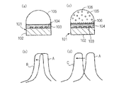
- Patent Document 1 discloses a surface acoustic wave sensor 101 shown in FIG.
- the surface acoustic wave sensor 101 is an IDT (inter-digital) which is an interdigital electrode for forming a surface acoustic wave element on a piezoelectric substrate 102.
- the electrode 103 and the reaction film 104 are formed, and the IDT electrode 103 is covered with the reaction film 104.
- the frequency characteristic detected by the surface acoustic wave element including the IDT electrode 103 changes.
- the substance 106 can be detected based on the fact that the frequency characteristics B and C differ depending on the presence or absence of the substance 106 that binds to the reaction film 104.
- Patent Document 2 discloses a surface acoustic wave sensor shown in FIG.
- FIG. 11A is a schematic plan view.
- FIG. 11B is a schematic cross-sectional view taken along the line AA in FIG.
- a circuit layer 211, an insulating layer 212, and a piezoelectric thin film 213 are sequentially formed on a substrate 210, and thin portions 214 and 215 are formed on the back surface of the piezoelectric substrate 210.
- FIG. 11A is a schematic plan view.
- FIG. 11B is a schematic cross-sectional view taken along the line AA in FIG.
- a circuit layer 211, an insulating layer 212, and a piezoelectric thin film 213 are sequentially formed on a substrate 210, and thin portions 214 and 215 are formed on the back surface of the piezoelectric substrate 210.
- thin portions 214 and 215 are formed on the back surface of the piezoelectric substrate 210.
- the IDT electrodes 222 and 223 of the first surface acoustic wave element 220 and the second IDT electrodes 224 and 225 of the surface acoustic wave element 221 are formed.
- This surface acoustic wave sensor detects changes in pressure and temperature by utilizing the fact that the oscillation frequency changes when distortion occurs in the thin portions 214 and 215 of the substrate 210 due to changes in pressure and temperature.
- the surface acoustic wave elements 220 and 221 can be prevented from being affected by ambient temperature changes, and an accurate pressure and temperature sensor can be realized. it can.
- the excitation modes of the surface acoustic wave elements 220 and 221 it is possible to select and combine Rayleigh waves, Sezawa waves, and Sezawa waves 2nd, or to select and combine higher-order excitation modes. Yes.
- Patent Document 2 does not mention sensitivity as a sensor.
- sensitivity when the configuration of Patent Document 2 is applied to a liquid concentration sensor or biosensor, if excitation is performed with Rayleigh waves or Sezawa waves having an SV component that is displaced in the direction perpendicular to the surface, a liquid or highly viscous substance is loaded on the excitation unit. When this occurs, vibration energy propagates to the sample side, causing a large characteristic deterioration, and the sensor does not function.
- the present invention is intended to provide a surface acoustic wave sensor that can improve detection sensitivity.
- the present invention provides a surface acoustic wave sensor configured as follows.
- the surface acoustic wave sensor includes: (a) a piezoelectric substrate; (b) an IDT electrode formed on the piezoelectric substrate; and (c) a protective film formed on the piezoelectric substrate so as to cover the IDT electrode. Is provided.
- the displacement in the surface direction of the surface of the protective film is opposite to the displacement in the surface direction near the boundary between the piezoelectric substrate and the protective film, and the surface of the protective film The surface is excited in a high-order mode of the SH wave that maximizes the amount of displacement in the surface direction.
- the surface acoustic wave mode used as a sensor is a high-order mode of the SH wave as in the above configuration
- the amount of displacement of the surface of the protective film, which is a sensing unit is increased as compared with a generally used basic mode. be able to. Therefore, the detection sensitivity with respect to the mass load on the surface of the protective film can be made larger than when the basic mode is used.
- the piezoelectric substrate is a LiNbO 3 substrate.
- the sound velocity of the higher-order mode wave of the SH wave is 1 with respect to the sound velocity of the surface acoustic wave excited in the fundamental mode of the SH wave by the surface acoustic wave element having only the IDT electrode on the LiNbO 3 substrate. .1 to 1.5 times.
- the protective film is a SiO 2 film.
- the film thickness of the SiO 2 film is 28% or more with respect to the wavelength of the surface acoustic wave excited in the fundamental mode of the SH wave by the surface acoustic wave element having only the IDT electrode on the piezoelectric substrate.
- the piezoelectric substrate is a LiNbO 3 substrate.
- the substrate orientation of the LiNbO 3 substrate is Euler angle (0 ⁇ 5 °, 60 to 170 °, 0 ⁇ 5 °).
- the IDT electrode is Au.
- the film thickness of the IDT electrode is 2% or more with respect to the wavelength of the surface acoustic wave excited in the fundamental mode of the SH wave by the surface acoustic wave element having only the IDT electrode on the piezoelectric substrate.
- the surface acoustic wave sensor of the present invention can improve detection sensitivity by using higher-order SH waves.
- Example 1 It is principal part sectional drawing which shows typically the structure of a surface acoustic wave sensor, (b) The top view which shows typically the structure of a surface acoustic wave element.
- Example 1 It is a graph which shows a frequency characteristic.
- Example 1 It is a graph which shows an impedance characteristic.
- Example 1 It is a graph which shows the displacement distribution of a depth direction.
- Example 1 It is a graph which shows the change of a frequency.
- Example 1 It is a graph which shows the relationship between an electromechanical coupling coefficient, (a) film thickness of a protective film, and (b) board
- Example 1 It is a graph which shows the relationship between the film thickness of a protective film, and the sound velocity of a resonance point.
- Example 1 It is a graph which shows the analysis result of the sensitivity at the time of using a higher-order mode.
- Example 2 It is a graph which shows the relationship between a displacement amount and a sensitivity.
- Example 3 It is explanatory drawing of a surface acoustic wave sensor.
- 2A is a schematic plan view of a surface acoustic wave sensor, and FIG. (Conventional example 2)
- Example 1 The configuration of the surface acoustic wave sensor 10 of Example 1 will be described with reference to FIGS.
- FIG. 1A is a cross-sectional view of an essential part schematically showing the configuration of the surface acoustic wave sensor 10.
- FIG. 1B is a plan view schematically showing the configuration of the surface acoustic wave element 11.
- the surface acoustic wave sensor 10 includes a surface acoustic wave element 11 (see FIG. 1B) including an IDT electrode 13 formed on a piezoelectric substrate 12 so as to cover the IDT electrode 13.
- a protective film 14 is formed. The surface 14s of the uppermost protective film 14 is exposed, and comes into contact with the sample 2 when the sample 2 is supplied. When there is a mass load substance such as DNA or protein in the sample 2, the mass load substance is deposited on the surface 14s of the uppermost protective film 14.
- the surface acoustic wave element 11 includes two IDT electrodes 13 arranged in the vibration propagation direction (left-right direction in the figure) of the surface acoustic wave and both sides of the vibration propagation direction. And a reflector 13x arranged.
- the IDT electrode 13 is composed of a pair of comb electrodes each having a plurality of electrode fingers 13s that are interleaved with each other. A voltage is applied between a pair of comb electrodes of one IDT electrode 13 to excite the surface acoustic wave, and the surface acoustic waves are detected by a voltage change between the pair of comb electrodes of the other IDT electrode 13.
- the surface acoustic wave is confined between the reflectors 13x.
- the protective film 14 (see FIG. 1A) is formed so as to cover the IDT electrode 13 and the reflector 13x.
- the surface acoustic wave sensor 10 has a frequency characteristic (for example, a resonance frequency) of the surface acoustic wave element 11 when the mass load contained in the sample 2 is deposited on the surface 14s of the uppermost protective film 14 and the mass load changes.
- the mass loading substance can be detected by changing.
- the IDT electrode 13 is formed of an Au film on the LiNbO 3 piezoelectric substrate 12 and the SiO 2 film is formed thereon as the insulating film 14 will be described.
- the thickness h 0 / ⁇ obtained by normalizing the thickness h 0 of the SiO 2 film of the insulating film 14 with the wavelength ⁇ is 0.2 or more, preferably 0.28 or more.
- the wavelength ⁇ used for normalization is the fundamental mode of the SH wave according to the pitch of the electrode fingers of the IDT electrode 13 when only the IDT electrode 13 is provided on the piezoelectric substrate 12 and the protective film 14 is not provided. This is the wavelength of the surface acoustic wave excited by.
- a mode called a high-order mode having a frequency 1.1 to 1.5 times the frequency of the fundamental mode can be generated.
- FIG. 2 is a graph showing frequency characteristics.
- the horizontal axis is frequency, and the vertical axis is insertion loss and phase.
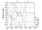
- FIG. 3 is a graph showing impedance characteristics.
- the horizontal axis is frequency, and the vertical axis is impedance and phase.
- the frequency on the horizontal axis is normalized by the frequency of the basic mode.
- Reference numeral 82 denotes a waveform portion in the basic mode
- reference numeral 84 denotes a waveform portion in the higher-order mode.
- FIG. 4 shows the result of analyzing the displacement distribution in the depth direction in the fundamental mode and the higher-order mode.
- the horizontal axis indicates the magnitude of displacement in the surface direction
- the vertical axis indicates the depth in the film thickness direction.
- the displacement becomes maximum near the boundary between the piezoelectric substrate 12 and the IDT electrode 13.
- a node enters the boundary between the piezoelectric substrate 12 and the IDT electrode 13, and the displacement of the surface 14 s of the protective film 14 is near the boundary between the piezoelectric substrate 12 and the IDT electrode 13.
- the direction is opposite to the displacement of.
- the displacement is maximized on the surface 14 s of the protective film 14.
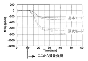
- FIG. 5 is a graph showing changes in the resonance frequency when the same sample is supplied to the surface acoustic wave sensor when the fundamental mode is used and when the higher-order mode is used.
- the horizontal axis is the elapsed time. Samples were fed after 10 minutes.
- the vertical axis represents the rate of change of the resonance frequency f, and the ratio of the deviation (f ⁇ f 0 ) of the resonance frequency to the initial resonance frequency f 0 , that is, (f ⁇ f 0 ) / f 0 is expressed in ppm (parts per million). Expressed in units.
- the data of a plurality of samples are shown for each of the basic mode and the higher-order mode.
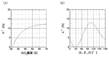
- FIG. 6A is a graph showing the relationship between the thickness h 0 / ⁇ of the protective film 14 of SiO 2 with respect to the wavelength ⁇ and the electromechanical coupling coefficient K 2 .
- the SiO 2 protective film 12 in the higher order mode, is excited when the film thickness h 0 / ⁇ is 20% or more, and is electromechanically coupled when the film thickness h 0 / ⁇ is 28% or more.
- factor K 2 is a relatively large value of 5% or more is obtained.
- FIG. 6 (b) is a graph showing the relationship between the substrate orientation and the electromechanical coefficient K 2 of the piezoelectric substrate 12 of LiNbO 3.
- the electromechanical coupling coefficient K 2 is 5% or more. Therefore, if the substrate orientation of the LiNbO 3 piezoelectric substrate 12 is expressed as Euler angles (0 ⁇ 5 °, 60 to 170 °, 0 ⁇ 5 °), the electromechanical coupling coefficient K 2 is 5% or more. It is expected that a relatively large value of can be obtained, which is preferable.
- FIG. 7 shows the relationship between the film thickness of the SiO 2 protective film 14 and the sound velocity at the resonance point of the surface acoustic wave for the higher-order mode and the fundamental mode.
- the horizontal axis represents the film thickness h 0 / ⁇ with respect to the wavelength ⁇ of the protective film 14 made of SiO 2 .
- the vertical axis represents the speed of sound at the resonance point.
- a symbol 80a indicates a basic mode.
- a symbol 81 indicates a high-order mode.
- Symbol 80b indicates a sound speed 1.1 times that of the basic mode.
- the sound velocity at the resonance point depends on the film thickness of the protective film 14. It can also be seen that in the higher order mode, the sound speed is 1.1 times or more that of the basic mode.
- a higher-order mode appears when the film thickness h 0 / ⁇ with respect to the wavelength ⁇ of the protective film 14 of SiO 2 is 20%.
- the sound speed at the resonance point of the higher-order mode when the film thickness h 0 / ⁇ is 20% is predicted from FIG. 7 to be 1.5 times the sound speed at the resonance point of the fundamental mode.
- the sound speed at the resonance point of the higher-order mode approaches 1.1 times the sound speed at the resonance point of the fundamental mode. Accordingly, the sound speed at the resonance point of the higher order mode is 1.1 to 1.5 times the sound speed at the resonance point of the fundamental mode.
- Example 2 In the structure of FIG. 1 of Example 1, sensitivity calculation for mass load was performed using a two-dimensional FEM.
- FIG. 8 shows the analysis result of sensitivity when the higher-order mode is used by changing the film thickness of the Au IDT electrode 13 and the SiO 2 protective film 14 formed on the LiNbO 3 piezoelectric substrate 12.
- the horizontal axis represents the film thickness h 1 / ⁇ of the Au IDT electrode 13 with respect to the wavelength ⁇ .
- the vertical axis represents the film thickness h 1 / ⁇ with respect to the wavelength ⁇ of the protective film 14 of SiO 2 .
- the film thickness h 1 / ⁇ of the Au IDT electrode 13 with respect to the wavelength ⁇ is 2% or more, it is preferable that the sensitivity is about 1.5 times (450 ppm) or more of the fundamental mode.
- the film thickness h 1 / ⁇ of the Au IDT electrode 13 with respect to the wavelength ⁇ is 3% or more, it is more preferable because sensitivity (600 ppm or more) twice or more that of the fundamental mode can be obtained. In this case, in the film thickness range of the vertical axis and the horizontal axis in FIG.
- the film thickness h 1 / ⁇ with respect to the wavelength ⁇ of the Au IDT electrode 13 is 3% or more, the displacement of the surface of the protective film is not maximized in the basic mode. The effect of using a higher-order mode that maximizes the displacement of the film surface is increased. Also from this, it is more preferable that the film thickness h 1 / ⁇ of the Au IDT electrode 13 with respect to the wavelength ⁇ is 3% or more.
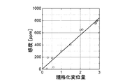
- Example 3 A graph summarizing the relationship between the amount of displacement and sensitivity of the protective film surface, which is the mass point load location, for the sensitivity analysis results for the mass load using the two-dimensional FEM shown in Examples 1 and 2. 9 shows.
- the amount of displacement on the horizontal axis is normalized by a certain amount of displacement when the fundamental mode is used under the same conditions (LiNbO 3 piezoelectric substrate, Au IDT electrode, SiO 2 insulating film).
- the sensitivity when the standardized displacement is 1 or less is the sensitivity when the basic mode is used.
- the sensitivity when the standardized displacement exceeds 1 is the sensitivity when the higher-order mode is used.
- the sensitivity can be improved by increasing the displacement of the mass load location using the higher order mode.
- the protective film is a sensing part.
- the displacement amount can be maximized on the surface, that is, the vibration energy can be concentrated on the sensing portion.
- the sensitivity as a sensor can be made larger than when the basic mode is used.
- the SH wave is less susceptible to vibration energy to be transmitted to the sample side and the energy loss is smaller than that of the SV wave, and therefore has high sensitivity to load fluctuations caused by the detection target substance and can function as a sensor. is there.
- the protective film may be a reaction film as shown in FIG.
- the present invention is not limited to a case where the sample is a liquid, but can also be applied to a case where the sample is a gas.
Landscapes
- Physics & Mathematics (AREA)
- Biochemistry (AREA)
- Health & Medical Sciences (AREA)
- Life Sciences & Earth Sciences (AREA)
- Chemical & Material Sciences (AREA)
- Analytical Chemistry (AREA)
- General Health & Medical Sciences (AREA)
- General Physics & Mathematics (AREA)
- Immunology (AREA)
- Pathology (AREA)
- Acoustics & Sound (AREA)
- Surface Acoustic Wave Elements And Circuit Networks Thereof (AREA)
- Investigating Or Analyzing Materials By The Use Of Ultrasonic Waves (AREA)
Abstract
検出感度を向上させることができる弾性表面波センサーを提供する。 弾性表面波センサー10は、(a)圧電基板12と、(b)圧電基板12上に形成されたIDT電極13と、(c)圧電基板12上に、IDT電極13を覆うように形成された保護膜14とを備える。弾性表面波センサー10は、IDT電極13により、保護膜14の表面14sの面方向の変位が圧電基板12と保護膜14との境界付近の面方向の変位とは逆向きになり、かつ保護膜14の表面14sにおいて面方向の変位量が最大となるSH波の高次モードで励振されるように構成されている。
Description
本発明は弾性表面波センサーに関し、詳しくは、弾性表面波素子の周波数特性が変化することを利用した弾性表面波センサーに関する。
従来、弾性表面波素子の励振部表面の質量負荷の変化に伴い、弾性表面波素子の周波数特性が変化することを利用した弾性表面波センサーが種々提案されている。
例えば、特許文献1には、図10に示す弾性表面波センサー101が開示されている。この弾性表面波センサー101は、図10(a)及び(c)の断面図に示すように、圧電基板102上に、弾性表面波素子を形成するためのすだれ状電極であるIDT(inter-digital transducer)電極103と反応膜104とが形成され、IDT電極103は反応膜104で覆われている。
図10(a)に示すように反応膜104上に液体105が接すると、IDT電極103を含む弾性表面波素子により検出される周波数特性が変化する。例えば、図10(b)の波形図において符号Aで示す周波数特性から符号Bで示す周波数特性に変化する。
一方、図10(c)に示すように反応膜104上に接する液体105中に、反応膜104と結合する物質106が存在すると、反応膜104に物質106が結合することによりIDT電極103への質量負荷が、液体105中に物質106が無い場合よりも、増加する。そのため、IDT電極103を含む弾性表面波素子により検出される周波数特性は、図10(d)の波形図において符号Aで示す周波数特性から符号Cで示す周波数特性に変化する。
このように反応膜104と結合する物質106の有無によって周波数特性B,Cが異なることに基づいて、物質106を検出することができる。
また、特許文献2には、図11に示す弾性表面波センサーが開示されている。図11(a)は模式平面図である。図11(b)は、図11(a)のA-A線に沿って切断された模式断面図である。図11(b)に示すように、基板210上に、回路層211、絶縁層212、圧電薄膜213が順に形成され、圧電基板210の裏面には薄肉部214,215が形成されている。図11(a)に示すように、基板210の薄肉部214,215に対応する圧電薄膜213の上には、それぞれ、第1の弾性表面波素子220のIDT電極222,223と、第2の弾性表面波素子221のIDT電極224,225とが形成されている。
この弾性表面波センサーは、圧力や温度の変化による基板210の薄肉部214,215に歪が生じると、発振周波数が変化することを利用して、圧力や温度の変化を検出するものである。弾性表面波素子220,221を別々の回路を用いて異なる周波数で励振することで、周囲の温度変化の影響を受けないようにすることができ、精度の良い圧力、温度センサーを実現することができる。弾性表面波素子220,221の励振モードとしては、レイリー波、セザワ波、セザワ波2ndを選択して組み合わせことや、高次の励振モードを選択して組み合わせ実施することも可能であるとされている。
特許文献1の弾性表面波センサーはSH波を用いているが、微量検出対象物に対して十分な感度が得られないことがあり、検出感度の向上が望まれている。
特許文献2では、センサーとしての感度については言及がない。また、液体の濃度センサーやバイオセンサーに特許文献2の構成を適用する場合、面垂直方向に変位するSV成分を持つレイリー波やセザワ波で励振すると、励振部に液体や粘性の高い物質が負荷された際に振動エネルギーが試料側に伝搬して大きな特性劣化を起こしてしまい、センサーとして機能しなくなる。
本発明は、かかる実情に鑑み、検出感度を向上させることができる弾性表面波センサーを提供しようとするものである。
本発明は、上記課題を解決するために、以下のように構成した弾性表面波センサーを提供する。
弾性表面波センサーは、(a)圧電基板と、(b)前記圧電基板上に形成されたIDT電極と、(c)前記圧電基板上に、前記IDT電極を覆うように形成された保護膜とを備える。弾性表面波センサーは、前記IDT電極により、前記保護膜の表面の面方向の変位が前記圧電基板と前記保護膜との境界付近の面方向の変位とは逆向きになり、かつ前記保護膜の前記表面において面方向の変位量が最大となるSH波の高次モードで励振されるように構成されている。
上記構成のように、センサーとして使用される弾性表面波のモードがSH波の高次モードであると、一般的に用いられる基本モードに比べ、センシング部である保護膜表面の変位量を大きくすることができる。そのため、保護膜表面への質量負荷に対する検出感度は、基本モードを用いた場合よりも大きくすることができる。
上記構成のようにSH波の高次モードを使用すると、液体センサーやバイオセンサーのように励振部であるIDT電極の上の保護膜表面に液体や粘性の大きい検出対象物質が付加されても、面方向の振動が伝搬されるのは保護膜表面の近傍領域に限られ、特性劣化が小さいため、センサーとして十分に機能させることが可能となる。これに対し、面に垂直方向に変位するSV波を使用する場合には、振動エネルギーが試料全体に伝搬して特性劣化が大きいため、液体センサーやバイオセンサーにはSV波を使用することができない。
具体的には、以下のように種々の態様で構成することができる。
好ましい一態様において、前記圧電基板は、LiNbO3基板である。前記SH波の前記高次モードの波の音速は、前記LiNbO3基板上に前記IDT電極のみを備えた弾性表面波素子によってSH波の基本モードで励振される弾性表面波の音速に対して1.1~1.5倍である。
好ましい他の態様において、前記保護膜は、SiO2膜である。前記SiO2膜の膜厚が、前記圧電基板上に前記IDT電極のみを備えた弾性表面波素子によってSH波の基本モードで励振される弾性表面波の波長に対して28%以上である。
この場合、SH波の高次モードが励振されたときに、電気機械結合係数K2が5%以上になるようにすることが、容易である。
好ましいさらに別の態様において、前記圧電基板がLiNbO3基板である。前記LiNbO3基板の基板方位が、オイラー角で(0±5°,60~170°,0±5°)である。
この場合、SH波の高次モードが励振されたときに、電気機械結合係数K2が5%以上になるようにすることが、容易である。
好ましいさらに別の態様において、前記IDT電極はAuである。前記IDT電極の膜厚が、前記圧電基板上に前記IDT電極のみを備えた弾性表面波素子によってSH波の基本モードで励振される弾性表面波の波長に対して2%以上である。
この場合、基本モードを用いる場合よりも高感度化することができる。
本発明の弾性表面波センサーは、高次のSH波を用いることにより、検出感度を向上させることができる。
以下、本発明の実施の形態について、図1~図9を参照しながら説明する。
<実施例1> 実施例1の弾性表面波センサー10の構成について、図1~図7を参照しながら説明する。
図1(a)は、弾性表面波センサー10の構成を模式的に示す要部断面図である。図1(b)は、弾性表面波素子11の構成を模式的に示す平面図である。
図1(a)に示すように、弾性表面波センサー10は、圧電基板12上にIDT電極13を含む弾性表面波素子11(図1(b)参照)が形成され、IDT電極13を覆うように保護膜14が形成されている。最上層の保護膜14の表面14sは露出しており、試料2が供給されると試料2に接する。試料2中にDNA、タンパク質等の質量負荷物質があると、最上層の保護膜14の表面14sに質量負荷物質が堆積する。
図1(b)に模式的に示すように、弾性表面波素子11は、弾性表面波の振動伝搬方向(図において左右方向)に配置された2つのIDT電極13と、その振動伝搬方向両側に配置された反射器13xとを有する。IDT電極13は、それぞれ互いに間挿し合う複数本の電極指13sを有する一対の櫛形電極により構成されている。一方のIDT電極13の一対の櫛型電極の間に電圧を印加して弾性表面波を励振し、他方のIDT電極13の一対の櫛型電極間の電圧変化によって弾性表面波を検出する。弾性表面波は、反射器13xの間に閉じ込められる。保護膜14(図1(a)参照)は、IDT電極13及び反射器13xを覆うように形成されている。
弾性表面波センサー10は、試料2に含まれている質量負荷物質が最上層の保護膜14の表面14sに堆積して質量負荷が変化すると、弾性表面波素子11の周波数特性(例えば共振周波数)が変化することによって、質量負荷物質を検出することができる。
以下において、LiNbO3の圧電基板12上に、Au膜によりIDT電極13が形成され、その上に、絶縁膜14としてSiO2膜が形成される場合について説明する。
この場合、詳しくは後述するが、絶縁膜14のSiO2膜の膜厚h0を波長λで規格化した膜厚h0/λが0.2以上、好ましくは0.28以上となるように形成する。また、IDT電極13の膜厚h1を波長λで規格化した膜厚h1/λが0.02以上になるように形成することが好ましい。ここで、規格化に用いた波長λは、圧電基板12上にIDT電極13のみを備え、保護膜14を備えていない場合において、IDT電極13の電極指のピッチに応じてSH波の基本モードで励振される弾性表面波の波長である。
このように構成することで、図2及び図3に示すように、基本モードの周波数の1.1~1.5倍の周波数の高次モードと呼ばれるモードが生じるようにすることができる。
すなわち、図2は周波数特性を示すグラフである。横軸は周波数、縦軸は挿入損失及び位相である。図3は、インピーダンス特性を示すグラフである。横軸は周波数、縦軸はインピーダンス及び位相である。横軸の周波数は、基本モードの周波数で規格化されている。符号82は基本モードの波形部分を示し、符号84は高次モードの波形部分を示す。
基本モードと高次モードとにおいて、いずれもSH波の面方向の変位が生じるが、図4に示すように、深さ方向の変位分布は異なる。
すなわち、図4は、基本モードと高次モードにおける深さ方向の変位分布を解析した結果を示す。横軸は面方向の変位の大きさ、縦軸は膜厚方向の深さを示す。破線は、IDT電極13の膜厚h1が波長λの2%、すなわちh1/λ=0.02の場合を示す。鎖線は、IDT電極13の膜厚h1が波長λの3%、すなわちh1/λ=0.03の場合を示す。実線は、IDT電極13の膜厚h1が波長λの4%、すなわちh1/λ=0.04の場合を示す。
図4の左側に示すように、基本モードでは、IDT電極13の膜厚h1が波長λの3%以上のとき、圧電基板12とIDT電極13との境界付近において変位が最大となる。
一方、図4の右側に示すように、高次モードでは、圧電基板12とIDT電極13との境界に一節入り、保護膜14の表面14sの変位は圧電基板12とIDT電極13との境界付近の変位とは逆方向になる。そして、保護膜14の表面14sにおいて変位が最大となる。
そのため、図5に示すように、高次モードを用いると、同じ質量負荷に対して基本モードを用いる場合より大きな感度(周波数変化)を得ることができる。
すなわち、図5は、基本モードを用いる場合と、高次モードを用いる場合とについて、弾性表面波センサーに同じ試料を供給したときの共振周波数の変化を示すグラフである。横軸は経過時間である。試料は10分経過後に供給した。縦軸は共振周波数fの変化率であり、初期共振周波数f0に対する共振周波数の偏差(f-f0)の割合、すなわち(f-f0)/f0をppm(百万分の1)単位で表している。基本モードと高次モードのそれぞれについて、複数のサンプルのデータを示している。
次に、高次モードを用いたときの電気機械結合係数K2の解析結果を説明する。
図6(a)は、SiO2の保護膜14の波長λに対する膜厚h0/λと、電気機械結合係数K2との関係を示すグラフである。図6(a)に示すように、高次モードは、SiO2の保護膜12の膜厚h0/λが20%以上で励振され、膜厚h0/λが28%以上で電気機械結合係数K2が5%以上の比較的大きな値が得られる。
図6(b)は、LiNbO3の圧電基板12の基板方位と電気機械係数K2との関係を示すグラフである。図6(b)に示すように、Y方向回転角θが60°以上になると電気機械結合係数K2が5%以上となる。このことから、LiNbO3の圧電基板12の基板方位としては、オイラー角表示で(0±5°、60~170°、0±5°)であれば、電気機械結合係数K2が5%以上の比較的大きな値が得られるものと期待でき、好ましい。
図7は、高次モードと基本モードについて、SiO2の保護膜14の膜厚と、弾性表面波の共振点における音速の関係を示す。横軸は、SiO2の保護膜14の波長λに対する膜厚h0/λである。縦軸は共振点における音速である。○記号80aは、基本モードを示す。●記号81は、高次モードを示す。・記号80bは、基本モードの1.1倍の音速を示す。
図8から、共振点の音速は、保護膜14の膜厚に依存することが分かる。また、高次モードでは、基本モードの音速の1.1倍以上の音速となることが分かる。
前述した図6から、SiO2の保護膜14の波長λに対する膜厚h0/λが20%で高次モードが現れる。この膜厚h0/λが20%であるときの高次モードの共振点の音速は、図7から、基本モードの共振点の音速の1.5倍と予測される。また、図8から、SiO2の保護膜14の膜厚が大きくなると、高次モードの共振点の音速は、基本モードの共振点の音速の1.1倍に近づく。したがって、高次モードの共振点の音速は、基本モードの共振点の音速の1.1~1.5倍となる。
<実施例2> 実施例1の図1の構造において、2次元FEMを用いて、質量負荷に対する感度計算を行なった。
図8に、LiNbO3の圧電基板12上に形成されるAuのIDT電極13の膜厚とSiO2の保護膜14の膜厚を変え、高次モードを用いたときの感度の解析結果を示す。横軸は、AuのIDT電極13の波長λに対する膜厚h1/λである。縦軸は、SiO2の保護膜14の波長λに対する膜厚h1/λである。
同じ条件で、基本モードを用いた時の感度を解析すると、約300ppmであった。このことから、2倍以上の感度(600ppm以上)が得られる条件としては、図6において符号60を付した実線より右側の範囲となる。
図8から分かるように、AuのIDT電極13の波長λに対する膜厚h1/λが2%以上であれば、基本モードの約1.5倍(450ppm)以上の感度が得られ、好ましい。
AuのIDT電極13の波長λに対する膜厚h1/λが3%以上であれば、基本モードの2倍以上の感度(600ppm以上)が得られるため、より好ましい。この場合、図8の縦軸及び横軸の膜厚範囲においては、基本モードの2~5倍の感度になる。
なお、図4の左側に示したように、AuのIDT電極13の波長λに対する膜厚h1/λが3%以上であれば、基本モードにおいて保護膜表面の変位が最大とならないため、保護膜表面の変位が最大となる高次モードを用いる効果が大きくなる。このことからも、AuのIDT電極13の波長λに対する膜厚h1/λが3%以上であれば、より好ましい。
<実施例3> 実施例1、2に示した2次元FEMを用いての質量負荷に対する感度解析結果等について、質点負荷箇所である保護膜表面の変位量と感度の関係をまとめたグラフを図9に示す。
図9において、横軸の変位量は、同じ条件(LiNbO3の圧電基板、AuのIDT電極、SiO2の絶縁膜)で基本モードを用いた場合のある特定の変位量で規格化されている。図9において、規格化された変位量が1以下のときの感度は、基本モードを用いる場合の感度である。規格化された変位量が1を越えるときの感度は、高次モードの用いる場合の感度である。
図9に示すように変位量と感度には相関があることから、高次モードを用いて質量負荷箇所の変位を大きくすることで、感度を向上させることできる。
ただし、変位量と感度の相関は構造や材料に依存しており、構造や材料を大きく変化させた場合には、図9の近似直線に沿うとは限らないことに注意が必要である。
<まとめ> 以上に説明したように、保護膜と圧電基板の境界と、保護膜表面とで変位方向が逆になるSH波の高次モードが発生するように構成すると、センシング部分である保護膜表面で最も変位量が大きくなるようにする、すなわちセンシング部分に振動エネルギーを集中させることができる。これによって、センサーとしての感度が、基本モードを用いた場合よりも大きくすることができる。
また、SH波であるため、液体センサーやバイオセンサーのように励振部の上に液体や粘性の大きな検出対象物質が負荷されても、特性劣化が小さく、センサーとして機能させることが可能である。すなわち、SH波は、SV波と比べると、振動エネルギーが試料側に伝達されにくく、エネルギー損失が小さいため、検出対象物質による負荷変動に対して、感度が大きく、センサーとして機能させることが可能である。
なお、本発明は、上記実施の形態に限定されるものではなく、種々変更を加えて実施することが可能である。
例えば、圧電基板、保護膜、IDT電極の材料は、例示したもの以外を用いても構わない。保護膜は、図10のような反応膜であっても構わない。
また、本発明は、試料が液体である場合に限らず、試料が気体である場合にも適用可能である。
2 試料
4 質量負荷物質
10,10a 弾性表面波センサー
11 弾性表面波素子
12 圧電基板
13 IDT電極
13x 反射器
14 保護膜
4 質量負荷物質
10,10a 弾性表面波センサー
11 弾性表面波素子
12 圧電基板
13 IDT電極
13x 反射器
14 保護膜
Claims (5)
- 圧電基板と、
前記圧電基板上に形成されたIDT電極と、
前記圧電基板上に、前記IDT電極を覆うように形成された保護膜と、
を備える弾性表面波センサーであって、
前記IDT電極により、前記保護膜の表面の面方向の変位が前記圧電基板と前記保護膜との境界付近の面方向の変位とは逆向きになり、かつ前記保護膜の前記表面において面方向の変位量が最大となるSH波の高次モードで励振されるように構成されたことを特徴とする、弾性表面波センサー。 - 前記圧電基板は、LiNbO3基板であり、
前記SH波の前記高次モードの波の音速は、前記LiNbO3基板上に前記IDT電極のみを備えた弾性表面波素子によってSH波の基本モードで励振される弾性表面波の音速に対して1.1~1.5倍であることを特徴とする、請求項1に記載の弾性表面波センサー。 - 前記保護膜は、SiO2膜であり、
前記SiO2膜の膜厚が、前記圧電基板上に前記IDT電極のみを備えた弾性表面波素子によってSH波の基本モードで励振される弾性表面波の波長に対して28%以上であることを特徴とする、請求項1又は2に記載の弾性表面波センサー。 - 前記圧電基板がLiNbO3基板であり、
前記LiNbO3基板の基板方位が、オイラー角で(0±5°,60~170°,0±5°)であることを特徴とする、請求項1、2又は3に記載の弾性表面波センサー。 - 前記IDT電極はAuであり、
前記IDT電極の膜厚が、前記圧電基板上に前記IDT電極のみを備えた弾性表面波素子によってSH波の基本モードで励振される弾性表面波の波長に対して2%以上であることを特徴とする、請求項1乃至4のいずれか一つに記載の弾性表面波センサー。
Priority Applications (2)
| Application Number | Priority Date | Filing Date | Title |
|---|---|---|---|
| JP2011519661A JP5170311B2 (ja) | 2009-06-25 | 2010-04-08 | 弾性表面波センサー |
| US13/315,309 US8207650B2 (en) | 2009-06-25 | 2011-12-09 | Surface acoustic wave sensor |
Applications Claiming Priority (2)
| Application Number | Priority Date | Filing Date | Title |
|---|---|---|---|
| JP2009-150419 | 2009-06-25 | ||
| JP2009150419 | 2009-06-25 |
Related Child Applications (1)
| Application Number | Title | Priority Date | Filing Date |
|---|---|---|---|
| US13/315,309 Continuation US8207650B2 (en) | 2009-06-25 | 2011-12-09 | Surface acoustic wave sensor |
Publications (1)
| Publication Number | Publication Date |
|---|---|
| WO2010150587A1 true WO2010150587A1 (ja) | 2010-12-29 |
Family
ID=43386368
Family Applications (1)
| Application Number | Title | Priority Date | Filing Date |
|---|---|---|---|
| PCT/JP2010/056370 Ceased WO2010150587A1 (ja) | 2009-06-25 | 2010-04-08 | 弾性表面波センサー |
Country Status (3)
| Country | Link |
|---|---|
| US (1) | US8207650B2 (ja) |
| JP (1) | JP5170311B2 (ja) |
| WO (1) | WO2010150587A1 (ja) |
Cited By (2)
| Publication number | Priority date | Publication date | Assignee | Title |
|---|---|---|---|---|
| JPWO2015137054A1 (ja) * | 2014-03-14 | 2017-04-06 | 株式会社村田製作所 | 弾性波装置 |
| JP2017072620A (ja) * | 2012-10-29 | 2017-04-13 | 京セラ株式会社 | 弾性表面波センサ |
Families Citing this family (6)
| Publication number | Priority date | Publication date | Assignee | Title |
|---|---|---|---|---|
| DE102017111448B4 (de) * | 2017-05-24 | 2022-02-10 | RF360 Europe GmbH | SAW-Vorrichtung mit unterdrückten Störmodensignalen |
| CN109187737B (zh) * | 2018-08-03 | 2023-09-01 | 山东鑫利达安防科技有限公司 | 一种基于saw器件的一氧化碳传感器及其浓度计算方法 |
| JP7163965B2 (ja) * | 2018-09-20 | 2022-11-01 | 株式会社村田製作所 | 弾性波装置 |
| CN111879853A (zh) * | 2020-07-16 | 2020-11-03 | 中国科学院声学研究所 | 一种剪切波模式的声表面波谐振式检测器 |
| CN116436432B (zh) * | 2023-04-17 | 2024-07-09 | 中国电子科技集团公司第二十六研究所 | 一种小型化的声表面波滤波器结构 |
| CN117013984B (zh) * | 2023-08-21 | 2024-05-28 | 天通瑞宏科技有限公司 | 一种键合晶圆及薄膜声表面波器件 |
Citations (4)
| Publication number | Priority date | Publication date | Assignee | Title |
|---|---|---|---|---|
| JPH02238357A (ja) * | 1989-03-13 | 1990-09-20 | Igaku Seibutsugaku Kenkyusho:Kk | 表面弾性波利用溶液センサ及び特定物質測定法 |
| JPH05240762A (ja) * | 1991-11-15 | 1993-09-17 | Hewlett Packard Co <Hp> | 表面横波装置 |
| WO2005003752A1 (ja) * | 2003-07-04 | 2005-01-13 | Murata Manufacturing Co., Ltd. | 弾性表面波センサー |
| JP2009109261A (ja) * | 2007-10-29 | 2009-05-21 | Tama Tlo Kk | 弾性表面波ガス・センサ装置 |
Family Cites Families (5)
| Publication number | Priority date | Publication date | Assignee | Title |
|---|---|---|---|---|
| US5130257A (en) | 1988-09-29 | 1992-07-14 | Hewlett-Packard Company | Chemical sensor utilizing a surface transverse wave device |
| WO2005083882A1 (en) * | 2004-02-26 | 2005-09-09 | Mnt Innovations Pty Ltd | Layered surface acoustic wave sensor |
| JP2007057287A (ja) | 2005-08-23 | 2007-03-08 | Seiko Epson Corp | 弾性表面波デバイス |
| JP5125729B2 (ja) * | 2008-04-28 | 2013-01-23 | パナソニック株式会社 | 弾性波素子と、これを用いたフィルタ及び電子機器 |
| JP2010088109A (ja) * | 2008-09-05 | 2010-04-15 | Panasonic Corp | 弾性波素子と、これを用いた電子機器 |
-
2010
- 2010-04-08 WO PCT/JP2010/056370 patent/WO2010150587A1/ja not_active Ceased
- 2010-04-08 JP JP2011519661A patent/JP5170311B2/ja active Active
-
2011
- 2011-12-09 US US13/315,309 patent/US8207650B2/en active Active
Patent Citations (4)
| Publication number | Priority date | Publication date | Assignee | Title |
|---|---|---|---|---|
| JPH02238357A (ja) * | 1989-03-13 | 1990-09-20 | Igaku Seibutsugaku Kenkyusho:Kk | 表面弾性波利用溶液センサ及び特定物質測定法 |
| JPH05240762A (ja) * | 1991-11-15 | 1993-09-17 | Hewlett Packard Co <Hp> | 表面横波装置 |
| WO2005003752A1 (ja) * | 2003-07-04 | 2005-01-13 | Murata Manufacturing Co., Ltd. | 弾性表面波センサー |
| JP2009109261A (ja) * | 2007-10-29 | 2009-05-21 | Tama Tlo Kk | 弾性表面波ガス・センサ装置 |
Cited By (2)
| Publication number | Priority date | Publication date | Assignee | Title |
|---|---|---|---|---|
| JP2017072620A (ja) * | 2012-10-29 | 2017-04-13 | 京セラ株式会社 | 弾性表面波センサ |
| JPWO2015137054A1 (ja) * | 2014-03-14 | 2017-04-06 | 株式会社村田製作所 | 弾性波装置 |
Also Published As
| Publication number | Publication date |
|---|---|
| US20120074809A1 (en) | 2012-03-29 |
| JP5170311B2 (ja) | 2013-03-27 |
| JPWO2010150587A1 (ja) | 2012-12-10 |
| US8207650B2 (en) | 2012-06-26 |
Similar Documents
| Publication | Publication Date | Title |
|---|---|---|
| JP5170311B2 (ja) | 弾性表面波センサー | |
| US9322809B2 (en) | Elastic wave sensor | |
| US7482732B2 (en) | Layered surface acoustic wave sensor | |
| JPWO2011030519A1 (ja) | 弾性波素子と弾性波素子センサ | |
| CN101198865A (zh) | 无线声学滤油器传感器 | |
| JPH10233645A (ja) | 弾性表面波装置 | |
| KR101711204B1 (ko) | 단일입력 다중출력 표면탄성파 디바이스 | |
| JP2008236295A (ja) | Saw共振子 | |
| US9518863B2 (en) | Elastic wave element and elastic wave sensor using same | |
| JP2007010378A (ja) | 弾性表面波素子及びその製造方法、弾性表面波センサ、並びに弾性表面波センサシステム | |
| JP6604238B2 (ja) | 弾性波センサ | |
| US7816837B2 (en) | Surface acoustic wave sensor | |
| JP2006313092A (ja) | 弾性表面波センサ及び弾性表面波センサシステム | |
| JP2007225546A (ja) | 弾性表面波センサ | |
| JP2005217818A (ja) | 圧電振動子 | |
| JP5431687B2 (ja) | 被測定物特性測定装置 | |
| JP5195926B2 (ja) | 弾性波センサー | |
| JP2008180668A (ja) | ラム波型高周波センサデバイス | |
| JP2005331326A (ja) | 弾性波センサ | |
| WO2010146923A1 (ja) | 弾性表面波センサー | |
| Seidel et al. | Multimode and multifrequency gigahertz surface acoustic wave sensors | |
| JP2007078428A (ja) | 弾性表面波センサ及び弾性表面波センサシステム | |
| JP2005315646A (ja) | 弾性表面波センサ及び弾性表面波センサシステム | |
| JPWO2010021100A1 (ja) | 弾性表面波センサー装置 | |
| WO2023189334A1 (ja) | 弾性波センサおよびその製造方法 |
Legal Events
| Date | Code | Title | Description |
|---|---|---|---|
| 121 | Ep: the epo has been informed by wipo that ep was designated in this application |
Ref document number: 10791907 Country of ref document: EP Kind code of ref document: A1 |
|
| WWE | Wipo information: entry into national phase |
Ref document number: 2011519661 Country of ref document: JP |
|
| NENP | Non-entry into the national phase |
Ref country code: DE |
|
| 122 | Ep: pct application non-entry in european phase |
Ref document number: 10791907 Country of ref document: EP Kind code of ref document: A1 |