WO2010146641A1 - 半導体装置及びその製造方法 - Google Patents
半導体装置及びその製造方法 Download PDFInfo
- Publication number
- WO2010146641A1 WO2010146641A1 PCT/JP2009/007345 JP2009007345W WO2010146641A1 WO 2010146641 A1 WO2010146641 A1 WO 2010146641A1 JP 2009007345 W JP2009007345 W JP 2009007345W WO 2010146641 A1 WO2010146641 A1 WO 2010146641A1
- Authority
- WO
- WIPO (PCT)
- Prior art keywords
- metal nitride
- film
- nitride film
- semiconductor device
- manufacturing
- Prior art date
- Legal status (The legal status is an assumption and is not a legal conclusion. Google has not performed a legal analysis and makes no representation as to the accuracy of the status listed.)
- Ceased
Links
Images


Classifications
-
- H—ELECTRICITY
- H10—SEMICONDUCTOR DEVICES; ELECTRIC SOLID-STATE DEVICES NOT OTHERWISE PROVIDED FOR
- H10D—INORGANIC ELECTRIC SEMICONDUCTOR DEVICES
- H10D64/00—Electrodes of devices having potential barriers
- H10D64/01—Manufacture or treatment
- H10D64/013—Manufacture or treatment of electrodes having a conductor capacitively coupled to a semiconductor by an insulator
- H10D64/01302—Manufacture or treatment of electrodes having a conductor capacitively coupled to a semiconductor by an insulator the insulator being formed after the semiconductor body, the semiconductor being silicon
- H10D64/01304—Manufacture or treatment of electrodes having a conductor capacitively coupled to a semiconductor by an insulator the insulator being formed after the semiconductor body, the semiconductor being silicon characterised by the conductor
- H10D64/01318—Manufacture or treatment of electrodes having a conductor capacitively coupled to a semiconductor by an insulator the insulator being formed after the semiconductor body, the semiconductor being silicon characterised by the conductor the conductor comprising a layer of alloy material, compound material or organic material contacting the insulator, e.g. TiN
-
- H—ELECTRICITY
- H10—SEMICONDUCTOR DEVICES; ELECTRIC SOLID-STATE DEVICES NOT OTHERWISE PROVIDED FOR
- H10D—INORGANIC ELECTRIC SEMICONDUCTOR DEVICES
- H10D64/00—Electrodes of devices having potential barriers
- H10D64/01—Manufacture or treatment
- H10D64/013—Manufacture or treatment of electrodes having a conductor capacitively coupled to a semiconductor by an insulator
- H10D64/01302—Manufacture or treatment of electrodes having a conductor capacitively coupled to a semiconductor by an insulator the insulator being formed after the semiconductor body, the semiconductor being silicon
- H10D64/01304—Manufacture or treatment of electrodes having a conductor capacitively coupled to a semiconductor by an insulator the insulator being formed after the semiconductor body, the semiconductor being silicon characterised by the conductor
- H10D64/01316—Manufacture or treatment of electrodes having a conductor capacitively coupled to a semiconductor by an insulator the insulator being formed after the semiconductor body, the semiconductor being silicon characterised by the conductor the conductor comprising a layer of elemental metal contacting the insulator, e.g. Ta, W, Mo or Al
-
- H—ELECTRICITY
- H10—SEMICONDUCTOR DEVICES; ELECTRIC SOLID-STATE DEVICES NOT OTHERWISE PROVIDED FOR
- H10D—INORGANIC ELECTRIC SEMICONDUCTOR DEVICES
- H10D64/00—Electrodes of devices having potential barriers
- H10D64/60—Electrodes characterised by their materials
- H10D64/66—Electrodes having a conductor capacitively coupled to a semiconductor by an insulator, e.g. MIS electrodes
- H10D64/667—Electrodes having a conductor capacitively coupled to a semiconductor by an insulator, e.g. MIS electrodes the conductor comprising a layer of alloy material, compound material or organic material contacting the insulator, e.g. TiN workfunction layers
- H10D64/669—Electrodes having a conductor capacitively coupled to a semiconductor by an insulator, e.g. MIS electrodes the conductor comprising a layer of alloy material, compound material or organic material contacting the insulator, e.g. TiN workfunction layers the conductor further comprising additional layers of alloy material, compound material or organic material, e.g. TaN/TiAlN
-
- H—ELECTRICITY
- H10—SEMICONDUCTOR DEVICES; ELECTRIC SOLID-STATE DEVICES NOT OTHERWISE PROVIDED FOR
- H10D—INORGANIC ELECTRIC SEMICONDUCTOR DEVICES
- H10D84/00—Integrated devices formed in or on semiconductor substrates that comprise only semiconducting layers, e.g. on Si wafers or on GaAs-on-Si wafers
- H10D84/01—Manufacture or treatment
- H10D84/0123—Integrating together multiple components covered by H10D12/00 or H10D30/00, e.g. integrating multiple IGBTs
- H10D84/0126—Integrating together multiple components covered by H10D12/00 or H10D30/00, e.g. integrating multiple IGBTs the components including insulated gates, e.g. IGFETs
- H10D84/0165—Integrating together multiple components covered by H10D12/00 or H10D30/00, e.g. integrating multiple IGBTs the components including insulated gates, e.g. IGFETs the components including complementary IGFETs, e.g. CMOS devices
- H10D84/0172—Manufacturing their gate conductors
- H10D84/0177—Manufacturing their gate conductors the gate conductors having different materials or different implants
-
- H—ELECTRICITY
- H10—SEMICONDUCTOR DEVICES; ELECTRIC SOLID-STATE DEVICES NOT OTHERWISE PROVIDED FOR
- H10D—INORGANIC ELECTRIC SEMICONDUCTOR DEVICES
- H10D84/00—Integrated devices formed in or on semiconductor substrates that comprise only semiconducting layers, e.g. on Si wafers or on GaAs-on-Si wafers
- H10D84/01—Manufacture or treatment
- H10D84/0123—Integrating together multiple components covered by H10D12/00 or H10D30/00, e.g. integrating multiple IGBTs
- H10D84/0126—Integrating together multiple components covered by H10D12/00 or H10D30/00, e.g. integrating multiple IGBTs the components including insulated gates, e.g. IGFETs
- H10D84/0165—Integrating together multiple components covered by H10D12/00 or H10D30/00, e.g. integrating multiple IGBTs the components including insulated gates, e.g. IGFETs the components including complementary IGFETs, e.g. CMOS devices
- H10D84/0181—Manufacturing their gate insulating layers
-
- H—ELECTRICITY
- H10—SEMICONDUCTOR DEVICES; ELECTRIC SOLID-STATE DEVICES NOT OTHERWISE PROVIDED FOR
- H10D—INORGANIC ELECTRIC SEMICONDUCTOR DEVICES
- H10D84/00—Integrated devices formed in or on semiconductor substrates that comprise only semiconducting layers, e.g. on Si wafers or on GaAs-on-Si wafers
- H10D84/01—Manufacture or treatment
- H10D84/02—Manufacture or treatment characterised by using material-based technologies
- H10D84/03—Manufacture or treatment characterised by using material-based technologies using Group IV technology, e.g. silicon technology or silicon-carbide [SiC] technology
- H10D84/038—Manufacture or treatment characterised by using material-based technologies using Group IV technology, e.g. silicon technology or silicon-carbide [SiC] technology using silicon technology, e.g. SiGe
-
- H—ELECTRICITY
- H10—SEMICONDUCTOR DEVICES; ELECTRIC SOLID-STATE DEVICES NOT OTHERWISE PROVIDED FOR
- H10D—INORGANIC ELECTRIC SEMICONDUCTOR DEVICES
- H10D30/00—Field-effect transistors [FET]
- H10D30/01—Manufacture or treatment
- H10D30/021—Manufacture or treatment of FETs having insulated gates [IGFET]
- H10D30/0223—Manufacture or treatment of FETs having insulated gates [IGFET] having source and drain regions or source and drain extensions self-aligned to sides of the gate
- H10D30/0227—Manufacture or treatment of FETs having insulated gates [IGFET] having source and drain regions or source and drain extensions self-aligned to sides of the gate having both lightly-doped source and drain extensions and source and drain regions self-aligned to the sides of the gate, e.g. lightly-doped drain [LDD] MOSFET or double-diffused drain [DDD] MOSFET
-
- H—ELECTRICITY
- H10—SEMICONDUCTOR DEVICES; ELECTRIC SOLID-STATE DEVICES NOT OTHERWISE PROVIDED FOR
- H10D—INORGANIC ELECTRIC SEMICONDUCTOR DEVICES
- H10D30/00—Field-effect transistors [FET]
- H10D30/60—Insulated-gate field-effect transistors [IGFET]
- H10D30/601—Insulated-gate field-effect transistors [IGFET] having lightly-doped drain or source extensions, e.g. LDD IGFETs or DDD IGFETs
-
- H—ELECTRICITY
- H10—SEMICONDUCTOR DEVICES; ELECTRIC SOLID-STATE DEVICES NOT OTHERWISE PROVIDED FOR
- H10D—INORGANIC ELECTRIC SEMICONDUCTOR DEVICES
- H10D64/00—Electrodes of devices having potential barriers
- H10D64/01—Manufacture or treatment
- H10D64/013—Manufacture or treatment of electrodes having a conductor capacitively coupled to a semiconductor by an insulator
- H10D64/01302—Manufacture or treatment of electrodes having a conductor capacitively coupled to a semiconductor by an insulator the insulator being formed after the semiconductor body, the semiconductor being silicon
- H10D64/01332—Making the insulator
- H10D64/01336—Making the insulator on single crystalline silicon, e.g. chemical oxidation using a liquid
- H10D64/01344—Making the insulator on single crystalline silicon, e.g. chemical oxidation using a liquid in a nitrogen-containing ambient, e.g. N2O oxidation
-
- H—ELECTRICITY
- H10—SEMICONDUCTOR DEVICES; ELECTRIC SOLID-STATE DEVICES NOT OTHERWISE PROVIDED FOR
- H10D—INORGANIC ELECTRIC SEMICONDUCTOR DEVICES
- H10D64/00—Electrodes of devices having potential barriers
- H10D64/60—Electrodes characterised by their materials
- H10D64/66—Electrodes having a conductor capacitively coupled to a semiconductor by an insulator, e.g. MIS electrodes
- H10D64/665—Electrodes having a conductor capacitively coupled to a semiconductor by an insulator, e.g. MIS electrodes the conductor comprising a layer of elemental metal contacting the insulator, e.g. tungsten or molybdenum
-
- H—ELECTRICITY
- H10—SEMICONDUCTOR DEVICES; ELECTRIC SOLID-STATE DEVICES NOT OTHERWISE PROVIDED FOR
- H10D—INORGANIC ELECTRIC SEMICONDUCTOR DEVICES
- H10D64/00—Electrodes of devices having potential barriers
- H10D64/60—Electrodes characterised by their materials
- H10D64/66—Electrodes having a conductor capacitively coupled to a semiconductor by an insulator, e.g. MIS electrodes
- H10D64/667—Electrodes having a conductor capacitively coupled to a semiconductor by an insulator, e.g. MIS electrodes the conductor comprising a layer of alloy material, compound material or organic material contacting the insulator, e.g. TiN workfunction layers
-
- H—ELECTRICITY
- H10—SEMICONDUCTOR DEVICES; ELECTRIC SOLID-STATE DEVICES NOT OTHERWISE PROVIDED FOR
- H10D—INORGANIC ELECTRIC SEMICONDUCTOR DEVICES
- H10D64/00—Electrodes of devices having potential barriers
- H10D64/60—Electrodes characterised by their materials
- H10D64/66—Electrodes having a conductor capacitively coupled to a semiconductor by an insulator, e.g. MIS electrodes
- H10D64/68—Electrodes having a conductor capacitively coupled to a semiconductor by an insulator, e.g. MIS electrodes characterised by the insulator, e.g. by the gate insulator
- H10D64/693—Electrodes having a conductor capacitively coupled to a semiconductor by an insulator, e.g. MIS electrodes characterised by the insulator, e.g. by the gate insulator the insulator comprising nitrogen, e.g. nitrides, oxynitrides or nitrogen-doped materials
Definitions
- the present invention relates to a semiconductor device including a transistor having a metal gate electrode and a method for manufacturing the same, and more particularly to improving characteristics of a transistor element having a metal gate electrode.
- the problem of the high-k / metal gate electrode structure is to realize a desired work function suitable for each of an NchFET (field-effect-transistor) (hereinafter referred to as NFET) and a PchFET (hereinafter referred to as PFET).
- NchFET field-effect-transistor
- PFET PchFET
- 4 (a) to 4 (g) are cross-sectional views showing respective steps of a transistor formation process according to a first conventional example using a high-k / metal gate electrode structure (see Patent Document 1).
- a trench type element isolation 2 is formed in a semiconductor substrate 1 to partition an NFET region and a PFET region, and then a high dielectric constant is formed on the semiconductor substrate 1.
- a gate insulating film 3 made of a rate insulator or the like is formed, and then a TiN film 5 having a thickness of about 20 nm is deposited on the gate insulating film 3.
- the TiN film 5 in the NFET region is removed by etching as shown in FIG. 4C. Thereafter, the mask pattern 6 is removed.
- a TiN film 7 having a thickness of about 2.5 nm is deposited on the entire surface of the semiconductor substrate 1, and then on the TiN film 7 as shown in FIG. 4E.
- a silicon film 8 is deposited.
- gate patterning is performed to form a gate electrode 9A composed of a TiN film 5, a TiN film 7, and a silicon film 8 in the PFET region, and TiN in the NFET region.
- a gate electrode 9B composed of the film 7 and the silicon film 8 is formed.
- insulating sidewall spacers 10 are formed on the side surfaces of the gate electrodes 9A and 9B, and source / source electrodes are formed on both sides of the gate electrodes 9A and 9B in the semiconductor substrate 1. Drain regions 11A and 11B are formed.
- the thick TiN film 5 and the thin TiN film 7 are used as metal electrodes in the PFET region, and the thin TiN film 7 is used as the metal electrode in the NFET region.
- a high work function is obtained in the PFET region and a low work function is obtained in the NFET region.
- FIGS. 5A to 5F are cross-sectional views showing respective steps of a transistor forming process according to a second conventional example using a high-k / metal gate electrode structure (see Patent Document 2).
- a trench type element isolation 2 is formed in a semiconductor substrate 1 to partition an NFET region and a PFET region, and then a high dielectric constant is formed on the semiconductor substrate 1.
- a gate insulating film 3 made of a rate insulator is formed, and then a TiN film 5 is deposited on the gate insulating film 3.
- a dose of about 1 ⁇ 10 14 cm ⁇ 2 is applied to the TiN film 5 in the NFET region.
- Nitrogen ions are implanted in an amount, and then the mask pattern 6 is removed as shown in FIG.
- the TiN film 5 in the NFET region is modified to a TiN film 5 ′ having a high nitrogen concentration.
- gate patterning is performed as shown in FIG. 5D, after a tungsten film 13 is formed on the entire surface of the semiconductor substrate 1, gate patterning is performed as shown in FIG. A gate electrode 9A composed of the film 5 and the tungsten film 13 is formed, and a gate electrode 9B composed of the TiN film 5 ′ and the tungsten film 13 is formed in the NFET region.
- insulating sidewall spacers 10 are formed on the side surfaces of the gate electrodes 9A and 9B, and source / source electrodes are formed on both sides of the gate electrodes 9A and 9B in the semiconductor substrate 1. Drain regions 11A and 11B are formed.
- the work function of the gate electrode (metal gate electrode) 9B in the NFET region is changed to the work function of the gate electrode 9A in the PFET region. It is lower than the function.
- the work function required for the NFET is about 4.3 eV or less, and the work function required for the PFET is about 4.9 eV or more, whereas in the first conventional example, the work function of the NFET Even if the thickness of the TiN film used for the gate electrode is about 2.5 nm and the thickness of the TiN film used for the gate electrode of the PFET is about 20 nm, the work functions of the NFET and the PFET are about 4.4 eV and 4.85 eV, respectively. Can only be set, and both are insufficient as required work functions.
- the work function of the NFET can only be reduced by about 0.1 eV, and a desired work function can be realized simultaneously for both the NFET and the PFET. I can't do it.
- an object of the present invention is to realize a work function value required for each polarity FET in a high-k / metal gate electrode structure.
- a first semiconductor device manufacturing method includes a first region in which a first conductivity type transistor is formed and a second region in which a second conductivity type transistor is formed.
- different types of gate insulating films may be formed in each transistor formation region.
- the first metal nitride film may be made of a metal nitride constituting the metal film.
- the metal constituting the metal film may be a metal (for example, Ta) different from the metal (for example, Ti) included in the first metal nitride film.
- the second metal nitride film is formed also on a portion of the gate insulating film located in the first region.
- a fifth gate electrode is formed by patterning at least the second metal nitride film, the first metal nitride film, and the metal film in the first region.
- a sixth step of forming a second gate electrode by patterning at least the second metal nitride film in the second region after the fourth step. Also good.
- a seventh step of forming a conductive film on the second metal nitride film after the fourth step and before each of the fifth step and the sixth step is performed.
- the first gate electrode is formed by patterning the conductive film, the second metal nitride film, the first metal nitride film, and the metal film
- the second gate electrode may be formed by patterning the conductive film and the second metal nitride film.
- an eighth step of changing the metal film to a third metal nitride film by performing a heat treatment at a temperature of 800 ° C. or higher after the seventh step may be further provided.
- the nitrogen concentration of the third metal nitride film may be lower than the nitrogen concentration of the first metal nitride film, and the gate insulating film contains nitrogen, and in the eighth step The nitrogen concentration of the gate insulating film may be reduced.
- the heat treatment for changing the metal film to the third metal nitride film may be, for example, an impurity activation heat treatment for forming a source / drain region. Further, after the eighth step, the lower portion of the metal film may remain as it is without being nitrided.
- a second semiconductor device manufacturing method includes a first region in which a first conductivity type transistor is formed and a second region in which a second conductivity type transistor is formed.
- the second metal nitride film is formed also on a portion of the gate insulating film located in the first region,
- a sixth step of forming a second gate electrode by patterning at least the second metal nitride film in the second region after the fourth step may be further included.
- a seventh step of forming a conductive film on the second metal nitride film after the fourth step and before each of the fifth step and the sixth step is performed.
- the first gate electrode is formed by patterning the conductive film, the second metal nitride film, and the first metal nitride film
- the second gate electrode may be formed by patterning the conductive film and the second metal nitride film.
- the first metal nitride film and the second metal nitride film may each be composed of TiN.
- the nitrogen concentration of the second metal nitride film may be higher than the nitrogen concentration of the first metal nitride film.
- the film thickness of the second metal nitride film may be smaller than the film thickness of the first metal nitride film.
- the gate insulating film may include a high dielectric constant insulating film.
- the high dielectric constant insulating film means an insulating film having a dielectric constant higher than that of SiO 2 .
- each of the first metal nitride film and the second metal nitride film may be deposited by a PVD (physical vapor deposition) method.
- each of the first metal nitride film and the second metal nitride film may be deposited by changing the ratio of the nitrogen gas flow rate to the total gas flow rate.
- the first conductivity type transistor may be a Pch transistor, and the second conductivity type transistor may be an Nch transistor, or Each of the first conductivity type transistor and the second conductivity type transistor may be the same conductivity type transistor.
- a semiconductor device includes a first gate insulating film formed on a first region in a semiconductor substrate, and a first gate electrode formed on the first gate insulating film.
- the first gate electrode includes a first metal nitride film and a second metal nitride film formed on the first metal nitride film and made of the same metal nitride as the first metal nitride film
- the nitrogen concentration and film thickness of the first metal nitride film are different from the nitrogen concentration and film thickness of the second metal nitride film.
- the first gate electrode may further include a conductive film formed on the second metal nitride film.
- the first gate electrode may further include a third metal nitride film formed under the first metal nitride film and having a nitrogen concentration lower than that of the first metal nitride film. You may have.
- the first gate electrode may further include a metal film formed under the third metal nitride film.
- each of the first metal nitride film and the second metal nitride film may be made of TiN.
- the nitrogen concentration of the second metal nitride film may be higher than the nitrogen concentration of the first metal nitride film.
- the film thickness of the second metal nitride film may be smaller than the film thickness of the first metal nitride film.
- the present invention after forming the first metal nitride film on each of the first region where the first conductivity type transistor is formed and the second region where the second conductivity type transistor is formed, A portion of the first metal nitride film located in the second region is removed, and then a second metal nitride made of the same metal nitride as the first metal nitride film is formed on the second region. A film is formed. Therefore, a metal electrode having a large film thickness and a low nitrogen concentration, that is, a gate electrode having a high work function can be formed in the first region, and a film thickness and a nitrogen concentration are small in the second region. A high metal electrode, that is, a gate electrode having a low work function can be formed. Therefore, the work function value required for each polarity FET in the high-k / metal gate electrode structure can be realized.
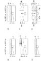
- FIG. 1A to 1H are cross-sectional views showing respective steps of a semiconductor device manufacturing method according to the first embodiment of the present invention.
- 2A to 2H are cross-sectional views showing respective steps of a method for manufacturing a semiconductor device according to the second embodiment of the present invention.
- FIG. 3 is a correlation diagram between the thickness of the TiN film in the gate electrode and the work function.
- 4A to 4G are cross-sectional views showing respective steps of the transistor forming process according to the first conventional example.
- 5A to 5F are cross-sectional views showing respective steps of the transistor forming process according to the second conventional example.
- FIGS. 1A to 1H are cross-sectional views showing respective steps of the method for manufacturing a semiconductor device according to the first embodiment.
- an element isolation 102 such as STI (shallow trench isolation) is formed on a semiconductor substrate 101 to partition an NFET region and a PFET region, and then a semiconductor substrate in each FET region. 101 is subjected to an impurity implantation for adjusting a threshold voltage (Vt) and an activation process, and thereafter an oxide film (not shown) on the surface of the semiconductor substrate 101 is removed.
- STI shallow trench isolation
- a thermal oxide film having a thickness of, for example, about 1.5 nm and a HfSiO film having a thickness of, for example, about 2.0 nm are sequentially deposited on the semiconductor substrate 101, and then the HfSiO film is nitrided to form HfSiON /
- a high dielectric constant gate insulating film 103 having a SiO 2 structure is formed.
- a Ti film 104 having a thickness of about 2 nm is deposited on the high dielectric constant gate insulating film 103 by using, for example, a PVD method, and then on the Ti film 104
- a TiN film 105 having a thickness of about 20 nm is deposited using the PVD method.
- the thickness of the Ti film 104 is selected from a numerical range of about 1 nm to 3 nm, for example.
- the thickness of the TiN film 105 is preferably selected from a relatively large numerical range, for example, a numerical range of about 10 nm to 30 nm.
- the nitrogen flow rate ratio (for example, (N 2 flow rate) / (Ar flow rate + N 2 flow rate)) when the TiN film 105 is deposited by the PVD method is set to a relatively low value of about 40%, whereby the nitrogen of the TiN film 105 is set.
- the concentration specifically, the composition ratio (molar ratio)
- the nitrogen flow rate ratio is set to a low flow rate ratio of 40% or less, a Ti film may be deposited without being deposited, so care must be taken.
- a mask pattern 106 having an opening in the NFET region is formed on the TiN film 105, a portion located in the NFET region as shown in FIG. 1C.
- the TiN film 105 and the Ti film 104 are removed by wet etching, for example, and then the mask pattern 106 is removed. As a result, the portion of the high dielectric constant gate insulating film 103 located in the NFET region is exposed.
- an etching solution having a high etching selectivity of the TiN film 105 to the high dielectric constant gate insulating film 103 and a relatively low etching rate of the TiN film 105 that is, an etching solution in which etching control is easy.
- a diluted SPM (sulfuric acid-hydrogen-peroxide mixture) solution may be used.
- the PVD method is used by setting the nitrogen flow rate ratio (for example, (N 2 flow rate) / (Ar flow rate + N 2 flow rate)) to about 80%, thereby depositing the TiN film 107 having a thickness of about 2 nm.
- the thickness of the TiN film 107 is preferably selected from a relatively small numerical range, for example, a numerical range of about 1 nm to 5 nm. Further, by selecting a nitrogen flow ratio when depositing the TiN film 107 by the PVD method from a relatively large numerical range, for example, a numerical range of about 80% to 100%, the nitrogen concentration of the TiN film 107 is made as high as possible. It is preferable to obtain a low work function.
- gate patterning is performed as shown in FIG. 1E.
- a gate electrode 109A composed of the Ti film 104, TiN film 105, TiN film 107, and polysilicon film 108 is formed in the PFET region, and a gate electrode 109B composed of the TiN film 107 and polysilicon film 108 is formed in the NFET region.
- the portions of the high dielectric constant gate insulating film 103 located outside the gate electrodes 109A and 109B are removed.
- an LDD (lightly doped doped drain) (111A) region 111A is formed in the PFET region and an NFET is formed.
- An LDD region 111B is formed in the region.
- insulating sidewall spacers 110 are formed on the side surfaces of the gate electrodes 109A and 109B.
- a source / drain region 112A is formed in the PFET region.
- source / drain regions 112B are formed in the NFET region.
- a silicide layer for example, Ni is formed on the gate electrodes 109A and 109B and the source / drain regions 112A and 112B. The transistor structure is completed.
- the ultrathin Ti film 104 included in the gate electrode 109A in the PFET region is subjected to the above-described impurity activation performed at a temperature of, for example, about 800 ° C. or higher during the process after the Ti film 104 is formed.
- nitrogen is removed from the TiN film 105 on the Ti film 104 to be modified into the TiN film 113 (see FIG. 1H).
- the lower part of the Ti film 104 may be left without being nitrided. If the Ti film 104 is very thin, the Ti film 104 may be modified to the TiN film 113 when the TiN film 105 is formed following the Ti film 104 formation.
- the nitrogen concentration of the TiN film 113 is lower than the nitrogen concentration of the TiN film 105 on the TiN film 113. Further, when the Ti film 104 is modified to the TiN film 113, the Ti film 104 also takes nitrogen from the lower high dielectric constant gate insulating film 103 (specifically, the HfSiON film), and the HfSiON film The nitrogen concentration may be lowered.
- the work function of the PFET can be set to about 4.9 eV or more.
- the TiN film 107 included in the gate electrode 109B in the NFET region is formed to have a relatively high nitrogen concentration and a thin film thickness of about 2 nm, both of which reduce the work function of the NFET. Acts as follows. Specifically, in this embodiment, the work function of the NFET can be set to about 4.3 eV or less.
- the gate electrode 109A having a metal electrode having a large film thickness and a low nitrogen concentration that is, the gate electrode 109A having a high work function can be formed.
- a gate electrode 109B having a metal electrode with a high concentration, that is, a gate electrode 109B with a low work function can be formed.
- the work function is adjusted so as to be adapted to each of the N-type and P-type reverse-polarity FETs.
- a plurality of FETs having the same polarity for example, memory FETs
- the work function may be adjusted by finely adjusting the thickness of the metal nitride film such as a TiN film or the nitrogen concentration so as to be suitable for the logic FET).
- the high dielectric constant gate insulating film 103 having the same configuration is formed in the NFET region and the PFET region, but instead, different types of gate insulating films may be formed in each FET region. .
- the work function can be further adjusted by adjusting the Hf concentration in the HfSiON layer constituting the high dielectric constant gate insulating film 103, for example.
- a non-nitrided HfSiO layer or HfO 2 layer may be used instead of HfSiON.
- a layer made of a material capable of changing the work function for example, a LaO layer, an AlO layer, a La layer, an Al layer, or the like is deposited on the high dielectric constant gate insulating film 103 in an extremely thin (about 1 nm). Further work function adjustments may be made.
- the TiN films 105 and 107 are formed by the PVD method. Instead, the TiN films 105 and 107 are formed by the ALD (atomic layer deposition) method or the CVD (chemical vapor deposition) method. May be.
- ALD atomic layer deposition
- CVD chemical vapor deposition
- the TiN films 105 and 107 are used as the metal nitride films constituting the gate electrodes 109A and 109B in the respective FET regions. Instead, other metal nitride films such as a TaN film are used. May be. Further, instead of the Ti film 104, a metal different from Ti contained in the TiN film 105, for example, a metal film made of Ta may be used.
- FIGS. 2A to 2H are cross-sectional views showing respective steps of the semiconductor device manufacturing method according to the second embodiment.
- an element isolation 102 such as STI is formed on a semiconductor substrate 101 to partition an NFET region and a PFET region, and then, in the semiconductor substrate 101 in each FET region. Impurity implantation for adjusting the threshold voltage (Vt) and activation processing are performed, and then the oxide film (not shown) on the surface of the semiconductor substrate 101 is removed.
- a thermal oxide film having a thickness of, for example, about 1.5 nm and a HfSiO film having a thickness of, for example, about 2.0 nm are sequentially deposited on the semiconductor substrate 101, and then the HfSiO film is nitrided to form HfSiON /
- a high dielectric constant gate insulating film 103 having a SiO 2 structure is formed.
- a TiN film 105 having a thickness of about 20 nm is deposited on the high dielectric constant gate insulating film 103 by using, for example, the PVD method.
- the thickness of the TiN film 105 is preferably selected from a relatively large numerical range, for example, a numerical range of about 10 nm to 30 nm.
- the nitrogen flow rate ratio (for example, (N 2 flow rate) / (Ar flow rate + N 2 flow rate)) when the TiN film 105 is deposited by the PVD method is set to a relatively low value of about 40%, whereby the nitrogen of the TiN film 105 is set.
- the concentration is as low as possible so that a high work function is obtained.
- the nitrogen flow rate ratio is set to a low flow rate ratio of 40% or less, a Ti film may be deposited without being deposited, so care must be taken.
- a mask pattern 106 having an opening in the NFET region is formed on the TiN film 105, and then a portion located in the NFET region as shown in FIG.
- the TiN film 105 is removed by wet etching, for example, and then the mask pattern 106 is removed.
- the portion of the high dielectric constant gate insulating film 103 located in the NFET region is exposed.
- the wet etching solution an etching solution having a high etching selectivity of the TiN film 105 to the high dielectric constant gate insulating film 103 and a relatively low etching rate of the TiN film 105 (that is, an etching solution in which etching control is easy).
- a diluted SPM solution may be used.
- the entire surface of the semiconductor substrate 101 including the portion of the high dielectric constant gate insulating film 103 located in the NFET region (that is, the exposed portion of the high dielectric constant gate insulating film 103).
- the PVD method is used by setting the nitrogen flow rate ratio (for example, (N 2 flow rate) / (Ar flow rate + N 2 flow rate)) to about 80%, thereby depositing the TiN film 107 having a thickness of about 2 nm.
- the thickness of the TiN film 107 is preferably selected from a relatively small numerical range, for example, a numerical range of about 1 nm to 5 nm. Further, by selecting a nitrogen flow ratio when depositing the TiN film 107 by the PVD method from a relatively large numerical range, for example, a numerical range of about 80% to 100%, the nitrogen concentration of the TiN film 107 is made as high as possible. It is preferable to obtain a low work function.
- a polysilicon film 108 having a thickness of, for example, about 100 nm is deposited on the TiN film 107, and then gate patterning is performed as shown in FIG.
- a gate electrode 109A composed of a TiN film 105, a TiN film 107, and a polysilicon film 108 is formed in the PFET region, and a gate electrode 109B composed of the TiN film 107 and the polysilicon film 108 is formed in the NFET region.
- the portions of the high dielectric constant gate insulating film 103 located outside the gate electrodes 109A and 109B are removed.
- impurities are implanted into the semiconductor substrate 101 using the gate electrodes 109A and 109B as a mask, thereby forming an LDD region 111A in the PFET region and an LDD region 111B in the NFET region.
- insulating sidewall spacers 110 are formed on the side surfaces of the gate electrodes 109A and 109B.
- the source / drain regions 112A are formed in the PFET region by implanting impurities into the semiconductor substrate 101 using the gate electrodes 109A and 109B and the insulating sidewall spacer 110 as a mask.
- source / drain regions 112B are formed in the NFET region.
- a silicide layer for example, Ni is formed on the gate electrodes 109A and 109B and the source / drain regions 112A and 112B.
- the transistor structure is completed.
- the total film thickness of the two-layer TiN films (TiN films 105 and 107) constituting the gate electrode 109A in the PFET region is as thick as about 22 nm.
- the nitrogen concentration of the TiN film is low as a whole, both of these act to increase the work function of the PFET.
- the work function of the PFET can be set to about 4.9 eV or more.
- the TiN film 107 included in the gate electrode 109B in the NFET region is formed to have a relatively high nitrogen concentration and a thin film thickness of about 2 nm, both of which reduce the work function of the NFET. Acts as follows. Specifically, in this embodiment, the work function of the NFET can be set to about 4.3 eV or less.
- FIG. 3 shows the correlation (thick line in the figure) between the film thickness of the TiN film in the gate electrode and the work function (this example), the first conventional example (Comparative Example 1) and the second conventional example (Comparative Example 2). ) And the work function value obtained by each.
- a work function of about 4.85 eV can be expected
- a work function of about 4.4 eV can be expected.
- a work function of about 4.9 eV can be obtained in the PFET and a work function of about 4.3 eV can be obtained in the NFET (in the drawing). ⁇ ). That is, since the work function required for the device is about 4.9 eV for PFET and about 4.3 eV for NFET, the work function required for any FET can be obtained according to this embodiment. Can do.
- the TiN film 105 having a large film thickness and a low nitrogen concentration is formed on each of the PFET region and the NFET region in the semiconductor substrate 101, and then located in the NFET region. A part of the TiN film 105 is removed, and then a TiN film 107 having a small film thickness and a high nitrogen concentration is formed on the NFET region. Therefore, in the PFET region, the gate electrode 109A having a metal electrode having a large film thickness and a low nitrogen concentration, that is, the gate electrode 109A having a high work function can be formed. A gate electrode 109B having a metal electrode with a high concentration, that is, a gate electrode 109B with a low work function can be formed.
- the work function is adjusted so as to be adapted to each of the N-type and P-type reverse-polarity FETs.
- a plurality of FETs having the same polarity for example, memory FETs
- the work function may be adjusted by finely adjusting the thickness of the metal nitride film such as the TiN film or the nitrogen concentration so as to be suitable for the logic FET).
- the high dielectric constant gate insulating film 103 having the same configuration is formed in the NFET region and the PFET region, but instead, different types of gate insulating films may be formed in each FET region. .
- the work function can be further adjusted by adjusting the Hf concentration in the HfSiON layer constituting the high dielectric constant gate insulating film 103, for example.
- a non-nitrided HfSiO layer or HfO 2 layer may be used instead of HfSiON.
- a layer made of a material capable of changing the work function for example, a LaO layer, an AlO layer, a La layer, an Al layer, or the like is deposited on the high dielectric constant gate insulating film 103 in an extremely thin (about 1 nm). Further work function adjustments may be made.
- the TiN films 105 and 107 are formed by the PVD method. Instead, the TiN films 105 and 107 may be formed by the ALD method or the CVD method.
- the TiN films 105 and 107 are used as the metal nitride films constituting the gate electrodes 109A and 109B in the respective FET regions. Instead, other metal nitride films such as a TaN film are used. May be.
- the present invention relates to a semiconductor device and a manufacturing method thereof, and is particularly useful for improving characteristics of a transistor element having a metal gate electrode.
Landscapes
- Electrodes Of Semiconductors (AREA)
- Metal-Oxide And Bipolar Metal-Oxide Semiconductor Integrated Circuits (AREA)
- Insulated Gate Type Field-Effect Transistor (AREA)
Abstract
第1の領域と第2の領域とを有する半導体基板(101)の上にゲート絶縁膜(103)を形成する。次に、ゲート絶縁膜(103)の上に第1の金属窒化膜(105)を堆積する。次に、第1の金属窒化膜(105)における第2の領域に位置する部分を除去することにより、ゲート絶縁膜(103)における第2の領域に位置する部分を露出させる。次に、ゲート絶縁膜(103)における第2の領域に位置する部分の上に、第1の金属窒化膜(105)と同じ金属窒化物からなる第2の金属窒化膜(107)を形成する。
Description
本発明は、メタルゲート電極を有するトランジスタを備えた半導体装置及びその製造方法に関し、特に、メタルゲート電極を有するトランジスタ素子の特性改善に関する。
デバイスの微細化や駆動力向上のために、従来のSiON/poly-Siゲート電極構造からHigh-k/metalゲート電極構造へのゲート構造変更の検討が進められている。High-k/metalゲート電極構造では、高誘電率絶縁膜により実効酸化膜厚(EOT)の低減とゲートリーク電流の低減との両立が可能であり、また、ゲート電極として金属膜を使用することにより、poly-Si電極で発生していたゲート空乏化を防止することができる。High-k/metalゲート電極構造の課題は、NchFET(field effect transistor)(以下、NFETという)及びPchFET(以下、PFETという)のそれぞれに適合した所望の仕事関数を実現することである。
図4(a)~(g)は、High-k/metalゲート電極構造を用いた第1従来例に係るトランジスタ形成プロセスの各工程を示す断面図である(特許文献1参照)。
第1従来例においては、まず、図4(a)に示すように、半導体基板1にトレンチ型素子分離2を形成してNFET領域とPFET領域とを区画した後、半導体基板1上に高誘電率絶縁体などからなるゲート絶縁膜3を形成し、その後、ゲート絶縁膜3上に厚さ20nm程度のTiN膜5を堆積する。
次に、図4(b)に示すように、TiN膜5上にPFET領域を覆うマスクパターン6を形成した後、図4(c)に示すように、NFET領域のTiN膜5をエッチングにより除去し、その後、マスクパターン6を除去する。
次に、図4(d)に示すように、半導体基板1上の全面に厚さ2.5nm程度のTiN膜7を堆積した後、図4(e)に示すように、TiN膜7上にシリコン膜8を堆積する。
次に、図4(f)に示すように、ゲートパターニングを行うことにより、PFET領域にはTiN膜5、TiN膜7及びシリコン膜8からなるゲート電極9Aを形成すると共に、NFET領域にはTiN膜7及びシリコン膜8からなるゲート電極9Bを形成する。
次に、図4(g)に示すように、ゲート電極9A及び9Bのそれぞれの側面に絶縁性サイドウォールスペーサ10を形成すると共に、半導体基板1におけるゲート電極9A及び9Bのそれぞれの両側にソース・ドレイン領域11A及び11Bを形成する。
以上のように、第1従来例においては、PFET領域では厚膜のTiN膜5と薄膜のTiN膜7とをメタル電極として使用すると共にNFET領域では薄膜のTiN膜7をメタル電極として使用することにより、PFET領域では高い仕事関数を得ていると共にNFET領域では低い仕事関数を得ている。
図5(a)~(f)は、High-k/metalゲート電極構造を用いた第2従来例に係るトランジスタ形成プロセスの各工程を示す断面図である(特許文献2参照)。
第2従来例においては、まず、図5(a)に示すように、半導体基板1にトレンチ型素子分離2を形成してNFET領域とPFET領域とを区画した後、半導体基板1上に高誘電率絶縁体からなるゲート絶縁膜3を形成し、その後、ゲート絶縁膜3上にTiN膜5を堆積する。
次に、図5(b)に示すように、TiN膜5上にPFET領域を覆うマスクパターン6を形成した後、NFET領域のTiN膜5に対して、1×1014cm-2程度のドーズ量で窒素イオンを注入し、その後、図5(c)に示すように、マスクパターン6を除去する。この窒素注入により、NFET領域のTiN膜5は高い窒素濃度を持つTiN膜5’に改質される。
次に、図5(d)に示すように、半導体基板1上の全面にタングステン膜13を形成した後、図5(e)に示すように、ゲートパターニングを行うことにより、PFET領域にはTiN膜5及びタングステン膜13からなるゲート電極9Aを形成すると共に、NFET領域にはTiN膜5’及びタングステン膜13からなるゲート電極9Bを形成する。
次に、図5(f)に示すように、ゲート電極9A及び9Bのそれぞれの側面に絶縁性サイドウォールスペーサ10を形成すると共に、半導体基板1におけるゲート電極9A及び9Bのそれぞれの両側にソース・ドレイン領域11A及び11Bを形成する。
以上のように、第2従来例においては、NFET領域のTiN膜5に窒素注入を実施することにより、NFET領域のゲート電極(メタルゲート電極)9Bの仕事関数をPFET領域のゲート電極9Aの仕事関数よりも低下させている。
しかしながら、前述の第1従来例及び第2従来例のいずれを用いたとしても、NFET及びPFETのそれぞれに適合した所望の仕事関数を実現することはできない。
具体的には、NFETに必要とされる仕事関数は4.3eV程度以下であり、PFETに必要とされる仕事関数は4.9eV程度以上であるのに対して、第1従来例においてNFETのゲート電極に用いるTiN膜の膜厚を2.5nm程度とし、PFETのゲート電極に用いるTiN膜の膜厚を20nm程度としても、NFET及びPFETの仕事関数をそれぞれ4.4eV程度及び4.85eV程度にしか設定することができず、いずれも必要とされる仕事関数としては不十分である。
また、第2従来例においてTiN膜に対する窒素注入によって仕事関数を調整しようとしても、NFETの仕事関数を0.1eV程度低下させることしかできず、NFET及びPFETの両方について同時に所望の仕事関数を実現することはできない。
前記に鑑み、本発明は、High-k/metalゲート電極構造において各極性のFETに要求される仕事関数値を実現することを目的とする。
前記の目的を達成するために、本発明に係る第1の半導体装置の製造方法は、第1導電型のトランジスタが形成される第1の領域と第2導電型のトランジスタが形成される第2の領域とを有する半導体基板の上にゲート絶縁膜を形成する第1の工程と、前記ゲート絶縁膜の上に、金属膜及び第1の金属窒化膜を順次堆積する第2の工程と、前記金属膜及び前記第1の金属窒化膜のそれぞれにおける前記第2の領域に位置する部分を除去することにより、前記ゲート絶縁膜における前記第2の領域に位置する部分を露出させる第3の工程と、前記第3の工程よりも後に、前記ゲート絶縁膜における前記第2の領域に位置する部分の上に、前記第1の金属窒化膜と同じ金属窒化物からなる第2の金属窒化膜を形成する第4の工程とを備えている。
本発明に係る第1の半導体装置の製造方法において、各トランジスタ形成領域で異なる種類のゲート絶縁膜を形成してもよい。
本発明に係る第1の半導体装置の製造方法において、前記第1の金属窒化膜は、前記金属膜を構成する金属の窒化物から構成されていてもよい。或いは、前記金属膜を構成する金属は、前記第1の金属窒化膜に含まれる金属(例えばTi)とは異なる金属(例えばTa)であってもよい。
本発明に係る第1の半導体装置の製造方法において、前記第4の工程では、前記ゲート絶縁膜における前記第1の領域に位置する部分の上にも前記第2の金属窒化膜を形成し、前記第4の工程よりも後に、前記第1の領域において少なくとも前記第2の金属窒化膜、前記第1の金属窒化膜及び前記金属膜をパターニングすることにより第1のゲート電極を形成する第5の工程と、前記第4の工程よりも後に、前記第2の領域において少なくとも前記第2の金属窒化膜をパターニングすることにより第2のゲート電極を形成する第6の工程とをさらに備えていてもよい。この場合、前記第4の工程よりも後で前記第5の工程及び前記第6の工程のそれぞれよりも前に、前記第2の金属窒化膜の上に導電膜を形成する第7の工程をさらに備え、前記第5の工程では、前記導電膜、前記第2の金属窒化膜、前記第1の金属窒化膜及び前記金属膜をパターニングすることにより前記第1のゲート電極を形成し、前記第6の工程では、前記導電膜及び前記第2の金属窒化膜をパターニングすることにより前記第2のゲート電極を形成してもよい。また、この場合、前記第7の工程よりも後に、800℃以上の温度で熱処理を行うことにより、前記金属膜を第3の金属窒化膜に変化させる第8の工程をさらに備えていてもよい。さらに、この場合、前記第3の金属窒化膜の窒素濃度は前記第1の金属窒化膜の窒素濃度よりも低くてもよいし、前記ゲート絶縁膜は窒素を含有し、前記第8の工程で前記ゲート絶縁膜の窒素濃度が減少してもよい。尚、前記金属膜を第3の金属窒化膜に変化させる熱処理は、例えばソース・ドレイン領域形成のための不純物活性化熱処理であってもよい。また、第8の工程の後に、金属膜の下部がそのまま窒化されずに残っていてもよい。
前記の目的を達成するために、本発明に係る第2の半導体装置の製造方法は、第1導電型のトランジスタが形成される第1の領域と第2導電型のトランジスタが形成される第2の領域とを有する半導体基板の上にゲート絶縁膜を形成する第1の工程と、前記ゲート絶縁膜の上に第1の金属窒化膜を堆積する第2の工程と、前記第1の金属窒化膜における前記第2の領域に位置する部分を除去することにより、前記ゲート絶縁膜における前記第2の領域に位置する部分を露出させる第3の工程と、前記第3の工程よりも後に、前記ゲート絶縁膜における前記第2の領域に位置する部分の上に、前記第1の金属窒化膜と同じ金属窒化物からなる第2の金属窒化膜を形成する第4の工程とを備え、前記第1の金属窒化膜の窒素濃度及び膜厚は前記第2の金属窒化膜の窒素濃度及び膜厚と異なっている。
本発明に係る第2の半導体装置の製造方法において、各トランジスタ形成領域で異なる種類のゲート絶縁膜を形成してもよい。
本発明に係る第2の半導体装置の製造方法において、前記第4の工程では、前記ゲート絶縁膜における前記第1の領域に位置する部分の上にも前記第2の金属窒化膜を形成し、前記第4の工程よりも後に、前記第1の領域において少なくとも前記第2の金属窒化膜及び前記第1の金属窒化膜をパターニングすることにより第1のゲート電極を形成する第5の工程と、前記第4の工程よりも後に、前記第2の領域において少なくとも前記第2の金属窒化膜をパターニングすることにより第2のゲート電極を形成する第6の工程とをさらに備えていてもよい。この場合、前記第4の工程よりも後で前記第5の工程及び前記第6の工程のそれぞれよりも前に、前記第2の金属窒化膜の上に導電膜を形成する第7の工程をさらに備え、前記第5の工程では、前記導電膜、前記第2の金属窒化膜及び前記第1の金属窒化膜をパターニングすることにより前記第1のゲート電極を形成し、前記第6の工程では、前記導電膜及び前記第2の金属窒化膜をパターニングすることにより前記第2のゲート電極を形成してもよい。
本発明に係る第1又は第2の半導体装置の製造方法において、前記第1の金属窒化膜及び前記第2の金属窒化膜はそれぞれTiNから構成されていてもよい。
本発明に係る第1又は第2の半導体装置の製造方法において、前記第2の金属窒化膜の窒素濃度は前記第1の金属窒化膜の窒素濃度よりも高くてもよい。
本発明に係る第1又は第2の半導体装置の製造方法において、前記第2の金属窒化膜の膜厚は前記第1の金属窒化膜の膜厚よりも薄くてもよい。
本発明に係る第1又は第2の半導体装置の製造方法において、前記ゲート絶縁膜は高誘電率絶縁膜を含んでいてもよい。ここで、高誘電率絶縁膜とは、SiO2 よりも高い誘電率を有する絶縁膜を意味する。
本発明に係る第1又は第2の半導体装置の製造方法において、前記第1の金属窒化膜及び前記第2の金属窒化膜のそれぞれをPVD(physical vapor deposition )法により堆積してもよい。この場合、前記第1の金属窒化膜及び前記第2の金属窒化膜のそれぞれを、総ガス流量に対する窒素ガス流量の比を変えて堆積してもよい。
本発明に係る第1又は第2の半導体装置の製造方法において、前記第1導電型のトランジスタはPchトランジスタであり、前記第2導電型のトランジスタはNchトランジスタであってもよいし、又は前記第1導電型のトランジスタ及び前記第2導電型のトランジスタのそれぞれは同一の導電型のトランジスタであってもよい。
本発明に係る半導体装置は、半導体基板における第1の領域の上に形成された第1のゲート絶縁膜と、前記第1のゲート絶縁膜の上に形成された第1のゲート電極とを備え、前記第1のゲート電極は、第1の金属窒化膜と、前記第1の金属窒化膜の上に形成され且つ前記第1の金属窒化膜と同じ金属窒化物からなる第2の金属窒化膜とを少なくとも有し、前記第1の金属窒化膜の窒素濃度及び膜厚は前記第2の金属窒化膜の窒素濃度及び膜厚と異なっている。
本発明に係る半導体装置において、前記第1のゲート電極は、前記第2の金属窒化膜の上に形成された導電膜をさらに有していてもよい。
本発明に係る半導体装置において、前記第1のゲート電極は、前記第1の金属窒化膜の下に形成され且つ前記第1の金属窒化膜よりも窒素濃度が低い第3の金属窒化膜をさらに有していてもよい。この場合、前記第1のゲート電極は、前記第3の金属窒化膜の下に形成された金属膜をさらに有していてもよい。
本発明に係る半導体装置において、前記第1の金属窒化膜及び前記第2の金属窒化膜はそれぞれTiNから構成されていてもよい。
本発明に係る半導体装置において、前記第2の金属窒化膜の窒素濃度は前記第1の金属窒化膜の窒素濃度よりも高くてもよい。
本発明に係る半導体装置において、前記第2の金属窒化膜の膜厚は前記第1の金属窒化膜の膜厚よりも薄くてもよい。
本発明に係る半導体装置において、前記半導体基板における第2の領域の上に形成された第2のゲート絶縁膜と、前記第2のゲート絶縁膜の上に形成された第2のゲート電極とをさらに備え、前記第2のゲート電極は、前記第2の金属窒化膜を少なくとも有していてもよい。この場合、前記第2のゲート絶縁膜は、前記第1のゲート絶縁膜と同じ絶縁膜であってもよい。
本発明によると、第1導電型のトランジスタが形成される第1の領域及び第2導電型のトランジスタが形成される第2の領域のそれぞれの上に第1の金属窒化膜を形成した後、前記第2の領域に位置する部分の第1の金属窒化膜を除去し、その後、前記第2の領域の上に、前記第1の金属窒化膜と同じ金属窒化物からなる第2の金属窒化膜を形成する。このため、第1の領域では、膜厚が大きく且つ窒素濃度が低いメタル電極、つまり仕事関数が高いゲート電極を形成することができると共に、第2の領域では、膜厚が小さく且つ窒素濃度が高いメタル電極、つまり仕事関数が低いゲート電極を形成することができる。従って、High-k/metalゲート電極構造において各極性のFETに要求される仕事関数値を実現することができる。
(第1の実施形態)
以下、本発明の第1の実施形態に係る半導体装置及びその製造方法を図面を参照しながら説明する。
以下、本発明の第1の実施形態に係る半導体装置及びその製造方法を図面を参照しながら説明する。
図1(a)~(h)は、第1の実施形態に係る半導体装置の製造方法の各工程を示す断面図である。
まず、図1(a)に示すように、半導体基板101に、例えばSTI(shallow trench isolation)などの素子分離102を形成してNFET領域とPFET領域とを区画した後、各FET領域の半導体基板101中に、しきい値電圧(Vt)調整のための不純物注入及び活性化処理を行い、その後、半導体基板101表面の酸化膜(図示省略)を除去する。続いて、半導体基板101上に、例えば厚さ1.5nm程度の熱酸化膜と、例えば厚さ2.0nm程度のHfSiO膜とを順次堆積した後、当該HfSiO膜を窒化することにより、HfSiON/SiO2 構造の高誘電率ゲート絶縁膜103を形成する。
次に、図1(a)に示すように、高誘電率ゲート絶縁膜103上に、例えばPVD法を用いて厚さ2nm程度のTi膜104を堆積し、続いて、Ti膜104上に、例えばPVD法を用いて厚さ20nm程度のTiN膜105を堆積する。
本実施形態では、Ti膜104の膜厚を例えば1nm~3nm程度の数値範囲から選択する。また、高い仕事関数を得るためにTiN膜105の膜厚を比較的大きい数値範囲、例えば10nm~30nm程度の数値範囲から選択することが好ましい。また、TiN膜105をPVD法により堆積する際の窒素流量比(例えば(N2 流量)/(Ar流量+N2 流量))を比較的低い40%程度に設定することにより、TiN膜105の窒素濃度(具体的には組成比(モル比))をできるだけ低くして高い仕事関数が得られるようにすることが好ましい。但し、窒素流量比を40%以下の低流量比に設定した場合には、TiN膜が堆積されずにTi膜が堆積される場合があるので、注意が必要である。
次に、図1(b)に示すように、TiN膜105上に、NFET領域に開口部を有するマスクパターン106を形成した後、図1(c)に示すように、NFET領域に位置する部分のTiN膜105及びTi膜104を例えばウェットエッチングによって除去し、続いて、マスクパターン106を除去する。これにより、NFET領域に位置する部分の高誘電率ゲート絶縁膜103が露出する。ここで、ウェットエッチング液としては、高誘電率ゲート絶縁膜103に対するTiN膜105のエッチング選択比が高く且つTiN膜105のエッチングレートが比較的小さいエッチング液(つまりエッチングの制御が容易なエッチング液)、例えば希釈SPM(sulfuric acid-hydrogen peroxide mixture )液を使用してもよい。
次に、図1(d)に示すように、NFET領域に位置する部分の高誘電率ゲート絶縁膜103(つまり高誘電率ゲート絶縁膜103の露出部分)の上を含む半導体基板101上の全面に、例えばPVD法を窒素流量比(例えば(N2 流量)/(Ar流量+N2 流量))を80%程度に設定して用いることによって、厚さ2nm程度のTiN膜107を堆積する。
本実施形態では、低い仕事関数を得るためにTiN膜107の膜厚を比較的小さい数値範囲、例えば1nm~5nm程度の数値範囲から選択することが好ましい。また、TiN膜107をPVD法により堆積する際の窒素流量比を比較的大きい数値範囲、例えば80%~100%程度の数値範囲から選択することにより、TiN膜107の窒素濃度をできるだけ高くして低い仕事関数が得られるようにすることが好ましい。
次に、図1(e)に示すように、TiN膜107上に例えば厚さ100nm程度のポリシリコン膜108を堆積した後、図1(f)に示すように、ゲートパターニングを行うことにより、PFET領域にはTi膜104、TiN膜105、TiN膜107及びポリシリコン膜108からなるゲート電極109Aを形成すると共に、NFET領域にはTiN膜107及びポリシリコン膜108からなるゲート電極109Bを形成する。このとき、ゲート電極109A及び109Bのそれぞれの外側に位置する部分の高誘電率ゲート絶縁膜103は除去される。
次に、図1(g)に示すように、ゲート電極109A及び109Bをマスクとして、半導体基板101に不純物注入を行うことにより、PFET領域にLDD(lightly doped drain )領域111Aを形成すると共に、NFET領域にLDD領域111Bを形成する。その後、ゲート電極109A及び109Bのそれぞれの側面に絶縁性サイドウォールスペーサ110を形成する。
次に、図1(h)に示すように、ゲート電極109A及び109B並びに絶縁性サイドウォールスペーサ110をマスクとして、半導体基板101に不純物注入を行うことにより、PFET領域にソース・ドレイン領域112Aを形成すると共に、NFET領域にソース・ドレイン領域112Bを形成する。その後、ソース・ドレイン領域112A及び112B中の不純物を活性化させるための熱処理を行った後、ゲート電極109A及び109B並びにソース・ドレイン領域112A及び112Bのそれぞれの上部に、例えばNiを含むシリサイド層(図示省略)を形成して、トランジスタ構造を完成させる。
本実施形態では、PFET領域のゲート電極109Aに含まれる極薄のTi膜104は、Ti膜104の形成後のプロセス処理中に、例えば800℃程度以上の温度で実施される前述の不純物活性化熱処理時に、Ti膜104上のTiN膜105中から窒素を奪い取ってTiN膜113に改質される(図1(h)参照)。ここで、Ti膜104の下部がそのまま窒化されずに残っていてもよい。また、Ti膜104が非常に薄い場合には、Ti膜104形成に続くTiN膜105形成時にTi膜104がTiN膜113に改質される場合もある。また、TiN膜113の窒素濃度は、TiN膜113上のTiN膜105の窒素濃度よりも低い。また、Ti膜104がTiN膜113に改質される際に、Ti膜104が、その下側の高誘電率ゲート絶縁膜103(具体的にはHfSiON膜)中からも窒素を奪い取り、HfSiON膜の窒素濃度が低下してもよい。
すなわち、Ti膜104がTiN膜113に改質されることにより、PFET領域のゲート電極109Aを構成する3層構造のTiN膜(TiN膜113、105及び107)のトータル膜厚は増加し、当該3層構造のTiN膜全体の窒素濃度が低下するか又は高誘電率ゲート絶縁膜103と接するように低窒素濃度のTiN膜113が形成され、高誘電率ゲート絶縁膜103となるHfSiON膜の窒素濃度は低下するが、これらはいずれもPFETの仕事関数を増大させるように作用する。具体的には、本実施形態ではPFETの仕事関数を4.9eV程度以上に設定することが可能である。
一方、NFET領域のゲート電極109Bに含まれるTiN膜107は、比較的高い窒素濃度と2nm程度の薄い膜厚とを持つように形成されているが、これらはいずれもNFETの仕事関数を低減させるように作用する。具体的には、本実施形態ではNFETの仕事関数を4.3eV程度以下に設定することが可能である。
以上に説明したように、本実施形態によると、半導体基板101におけるPFET領域及びNFET領域のそれぞれの上に、Ti膜104、及び膜厚が大きく且つ窒素濃度が低いTiN膜105を形成した後、NFET領域に位置する部分のTiN膜105及びTi膜104を除去し、その後、NFET領域の上に、膜厚が小さく且つ窒素濃度が高いTiN膜107を形成する。このため、PFET領域では、膜厚が大きく且つ窒素濃度が低いメタル電極を有するゲート電極109A、つまり仕事関数が高いゲート電極109Aを形成することができると共に、NFET領域では、膜厚が小さく且つ窒素濃度が高いメタル電極を有するゲート電極109B、つまり仕事関数が低いゲート電極109Bを形成することができる。
従って、High-k/metalゲート電極構造において各極性のFETに要求される仕事関数値を実現することができる。
尚、本実施形態において、N型及びP型の逆極性の複数のFETにそれぞれ適合するように仕事関数の調整を行ったが、これに代えて、同極性の複数のFET(例えばメモリ用FETとロジック用FET)にそれぞれ適合するように、TiN膜等の金属窒化膜の膜厚や窒素濃度を微調整することにより仕事関数の調整を行ってもよい。
また、本実施形態において、NFET領域とPFET領域とで同じ構成の高誘電率ゲート絶縁膜103を形成したが、これに代えて、各FET領域で異なる種類のゲート絶縁膜を形成してもよい。この場合、例えば高誘電率ゲート絶縁膜103を構成するHfSiON層中のHf濃度を調整することにより、さらなる仕事関数の調整を行うことができる。また、高誘電率ゲート絶縁膜103を構成する高誘電率層として、HfSiONに代えて、窒化していないHfSiO層やHfO2 層を使用してもよい。また、高誘電率ゲート絶縁膜103上に、仕事関数を変化させることができる材料からなる層、例えばLaO層、AlO層、La層、Al層などを極薄(1nm程度)で堆積することにより、さらなる仕事関数の調整を行ってもよい。
また、本実施形態において、PVD法によりTiN膜105及び107を成膜したが、これに代えて、ALD(atomic layer deposition )法やCVD(chemical vapor deposition )法によりTiN膜105及び107を成膜してもよい。
また、本実施形態において、各FET領域のゲート電極109A及び109Bを構成する金属窒化膜として、TiN膜105及び107を用いたが、これに代えて、TaN膜等の他の金属窒化膜を用いてもよい。また、Ti膜104に代えて、TiN膜105に含まれるTiとは異なる金属、例えばTaからなる金属膜を用いてもよい。
(第2の実施形態)
以下、本発明の第2の実施形態に係る半導体装置及びその製造方法を図面を参照しながら説明する。
以下、本発明の第2の実施形態に係る半導体装置及びその製造方法を図面を参照しながら説明する。
図2(a)~(h)は、第2の実施形態に係る半導体装置の製造方法の各工程を示す断面図である。
まず、図2(a)に示すように、半導体基板101に、例えばSTIなどの素子分離102を形成してNFET領域とPFET領域とを区画した後、各FET領域の半導体基板101中に、しきい値電圧(Vt)調整のための不純物注入及び活性化処理を行い、その後、半導体基板101表面の酸化膜(図示省略)を除去する。続いて、半導体基板101上に、例えば厚さ1.5nm程度の熱酸化膜と、例えば厚さ2.0nm程度のHfSiO膜とを順次堆積した後、当該HfSiO膜を窒化することにより、HfSiON/SiO2 構造の高誘電率ゲート絶縁膜103を形成する。
次に、図2(b)に示すように、高誘電率ゲート絶縁膜103上に、例えばPVD法を用いて厚さ20nm程度のTiN膜105を堆積する。
本実施形態では、高い仕事関数を得るためにTiN膜105の膜厚を比較的大きい数値範囲、例えば10nm~30nm程度の数値範囲から選択することが好ましい。また、TiN膜105をPVD法により堆積する際の窒素流量比(例えば(N2 流量)/(Ar流量+N2 流量))を比較的低い40%程度に設定することにより、TiN膜105の窒素濃度をできるだけ低くして高い仕事関数が得られるようにすることが好ましい。但し、窒素流量比を40%以下の低流量比に設定した場合には、TiN膜が堆積されずにTi膜が堆積される場合があるので、注意が必要である。
次に、図2(b)に示すように、TiN膜105上に、NFET領域に開口部を有するマスクパターン106を形成した後、図2(c)に示すように、NFET領域に位置する部分のTiN膜105を例えばウェットエッチングによって除去し、続いて、マスクパターン106を除去する。これにより、NFET領域に位置する部分の高誘電率ゲート絶縁膜103が露出する。ここで、ウェットエッチング液としては、高誘電率ゲート絶縁膜103に対するTiN膜105のエッチング選択比が高く且つTiN膜105のエッチングレートが比較的小さいエッチング液(つまりエッチングの制御が容易なエッチング液)、例えば希釈SPM液を使用してもよい。
次に、図2(d)に示すように、NFET領域に位置する部分の高誘電率ゲート絶縁膜103(つまり高誘電率ゲート絶縁膜103の露出部分)の上を含む半導体基板101上の全面に、例えばPVD法を窒素流量比(例えば(N2 流量)/(Ar流量+N2 流量))を80%程度に設定して用いることによって、厚さ2nm程度のTiN膜107を堆積する。
本実施形態では、低い仕事関数を得るためにTiN膜107の膜厚を比較的小さい数値範囲、例えば1nm~5nm程度の数値範囲から選択することが好ましい。また、TiN膜107をPVD法により堆積する際の窒素流量比を比較的大きい数値範囲、例えば80%~100%程度の数値範囲から選択することにより、TiN膜107の窒素濃度をできるだけ高くして低い仕事関数が得られるようにすることが好ましい。
次に、図2(e)に示すように、TiN膜107上に例えば厚さ100nm程度のポリシリコン膜108を堆積した後、図2(f)に示すように、ゲートパターニングを行うことにより、PFET領域にはTiN膜105、TiN膜107及びポリシリコン膜108からなるゲート電極109Aを形成すると共に、NFET領域にはTiN膜107及びポリシリコン膜108からなるゲート電極109Bを形成する。このとき、ゲート電極109A及び109Bのそれぞれの外側に位置する部分の高誘電率ゲート絶縁膜103は除去される。
次に、図2(g)に示すように、ゲート電極109A及び109Bをマスクとして、半導体基板101に不純物注入を行うことにより、PFET領域にLDD領域111Aを形成すると共に、NFET領域にLDD領域111Bを形成する。その後、ゲート電極109A及び109Bのそれぞれの側面に絶縁性サイドウォールスペーサ110を形成する。
次に、図2(h)に示すように、ゲート電極109A及び109B並びに絶縁性サイドウォールスペーサ110をマスクとして、半導体基板101に不純物注入を行うことにより、PFET領域にソース・ドレイン領域112Aを形成すると共に、NFET領域にソース・ドレイン領域112Bを形成する。その後、ソース・ドレイン領域112A及び112B中の不純物を活性化させるための熱処理を行った後、ゲート電極109A及び109B並びにソース・ドレイン領域112A及び112Bのそれぞれの上部に、例えばNiを含むシリサイド層(図示省略)を形成して、トランジスタ構造を完成させる。
本実施形態における最終的なゲート電極構造においては、PFET領域のゲート電極109Aを構成する2層構造のTiN膜(TiN膜105及び107)のトータル膜厚は22nm程度と厚く、当該2層構造のTiN膜の窒素濃度は全体として低いが、これらはいずれもPFETの仕事関数を増大させるように作用する。具体的には、本実施形態ではPFETの仕事関数を4.9eV程度以上に設定することが可能である。
一方、NFET領域のゲート電極109Bに含まれるTiN膜107は、比較的高い窒素濃度と2nm程度の薄い膜厚とを持つように形成されているが、これらはいずれもNFETの仕事関数を低減させるように作用する。具体的には、本実施形態ではNFETの仕事関数を4.3eV程度以下に設定することが可能である。
図3は、ゲート電極中のTiN膜の膜厚と仕事関数との相関関係(図中の太線)を、本実施形態、第1従来例(比較例1)及び第2従来例(比較例2)のそれぞれによって得られる仕事関数値と合わせて示している。図3の相関関係に示すように、TiN膜の膜厚を22nm程度に設定することにより、4.85eV程度の仕事関数が期待できると共に、TiN膜の膜厚を2nm程度に設定することにより、4.4eV程度の仕事関数が期待できる。さらに、本実施形態で説明したようにTiN膜中の窒素濃度を調整することにより、PFETでは4.9eV程度の仕事関数が得られると共にNFETでは4.3eV程度の仕事関数が得られる(図中の●)。すなわち、デバイスに対して要求される仕事関数はPFETで約4.9eV程度、NFETで約4.3eV程度であるので、本実施形態により、いずれのFETについても、要求される仕事関数を得ることができる。
それに対して、図3の比較例1(図中の◆)に示すように、TiN膜の膜厚をそれぞれ2.5nm及び20nmに設定しても、対応する仕事関数をそれぞれ4.4eV程度及び4.85eV程度までしか変化させることができず、いずれも必要とされる仕事関数としては不十分である。また、図3の比較例2(図中の▲)に示すように、TiN膜に対する窒素注入によって仕事関数を調整しようとしても、NFETの仕事関数を0.1eV程度低下させることしかできず、NFET及びPFETの両方について同時に所望の仕事関数を実現することはできない。
以上に説明したように、本実施形態によると、半導体基板101におけるPFET領域及びNFET領域のそれぞれの上に、膜厚が大きく且つ窒素濃度が低いTiN膜105を形成した後、NFET領域に位置する部分のTiN膜105を除去し、その後、NFET領域の上に、膜厚が小さく且つ窒素濃度が高いTiN膜107を形成する。このため、PFET領域では、膜厚が大きく且つ窒素濃度が低いメタル電極を有するゲート電極109A、つまり仕事関数が高いゲート電極109Aを形成することができると共に、NFET領域では、膜厚が小さく且つ窒素濃度が高いメタル電極を有するゲート電極109B、つまり仕事関数が低いゲート電極109Bを形成することができる。
従って、High-k/metalゲート電極構造において各極性のFETに要求される仕事関数値を実現することができる。
尚、本実施形態において、N型及びP型の逆極性の複数のFETにそれぞれ適合するように仕事関数の調整を行ったが、これに代えて、同極性の複数のFET(例えばメモリ用FETとロジック用FET)にそれぞれ適合するように、TiN膜等の金属窒化膜の膜厚や窒素濃度を微調整することにより仕事関数の調整を行ってもよい。
また、本実施形態において、NFET領域とPFET領域とで同じ構成の高誘電率ゲート絶縁膜103を形成したが、これに代えて、各FET領域で異なる種類のゲート絶縁膜を形成してもよい。この場合、例えば高誘電率ゲート絶縁膜103を構成するHfSiON層中のHf濃度を調整することにより、さらなる仕事関数の調整を行うことができる。また、高誘電率ゲート絶縁膜103を構成する高誘電率層として、HfSiONに代えて、窒化していないHfSiO層やHfO2 層を使用してもよい。また、高誘電率ゲート絶縁膜103上に、仕事関数を変化させることができる材料からなる層、例えばLaO層、AlO層、La層、Al層などを極薄(1nm程度)で堆積することにより、さらなる仕事関数の調整を行ってもよい。
また、本実施形態において、PVD法によりTiN膜105及び107を成膜したが、これに代えて、ALD法やCVD法によりTiN膜105及び107を成膜してもよい。
また、本実施形態において、各FET領域のゲート電極109A及び109Bを構成する金属窒化膜として、TiN膜105及び107を用いたが、これに代えて、TaN膜等の他の金属窒化膜を用いてもよい。
本発明は、半導体装置及びその製造方法に関し、特に、メタルゲート電極を有するトランジスタ素子の特性改善に有用である。
101 半導体基板
102 素子分離
103 高誘電率ゲート絶縁膜
104 Ti膜
105 TiN膜
106 マスクパターン
107 TiN膜
108 ポリシリコン膜
109A、109B ゲート電極
110 絶縁性サイドウォールスペーサ
111A、111B LDD領域
112A、112B ソース・ドレイン領域
113 TiN膜
102 素子分離
103 高誘電率ゲート絶縁膜
104 Ti膜
105 TiN膜
106 マスクパターン
107 TiN膜
108 ポリシリコン膜
109A、109B ゲート電極
110 絶縁性サイドウォールスペーサ
111A、111B LDD領域
112A、112B ソース・ドレイン領域
113 TiN膜
Claims (26)
- 第1導電型のトランジスタが形成される第1の領域と第2導電型のトランジスタが形成される第2の領域とを有する半導体基板の上にゲート絶縁膜を形成する第1の工程と、
前記ゲート絶縁膜の上に、金属膜及び第1の金属窒化膜を順次堆積する第2の工程と、
前記金属膜及び前記第1の金属窒化膜のそれぞれにおける前記第2の領域に位置する部分を除去することにより、前記ゲート絶縁膜における前記第2の領域に位置する部分を露出させる第3の工程と、
前記第3の工程よりも後に、前記ゲート絶縁膜における前記第2の領域に位置する部分の上に、前記第1の金属窒化膜と同じ金属窒化物からなる第2の金属窒化膜を形成する第4の工程とを備えていることを特徴とする半導体装置の製造方法。 - 請求項1に記載の半導体装置の製造方法において、
前記第1の金属窒化膜は、前記金属膜を構成する金属の窒化物からなることを特徴とする半導体装置の製造方法。 - 請求項1に記載の半導体装置の製造方法において、
前記第4の工程では、前記ゲート絶縁膜における前記第1の領域に位置する部分の上にも前記第2の金属窒化膜を形成し、
前記第4の工程よりも後に、前記第1の領域において少なくとも前記第2の金属窒化膜、前記第1の金属窒化膜及び前記金属膜をパターニングすることにより第1のゲート電極を形成する第5の工程と、
前記第4の工程よりも後に、前記第2の領域において少なくとも前記第2の金属窒化膜をパターニングすることにより第2のゲート電極を形成する第6の工程とをさらに備えていることを特徴とする半導体装置の製造方法。 - 請求項3に記載の半導体装置の製造方法において、
前記第4の工程よりも後で前記第5の工程及び前記第6の工程のそれぞれよりも前に、前記第2の金属窒化膜の上に導電膜を形成する第7の工程をさらに備え、
前記第5の工程では、前記導電膜、前記第2の金属窒化膜、前記第1の金属窒化膜及び前記金属膜をパターニングすることにより前記第1のゲート電極を形成し、
前記第6の工程では、前記導電膜及び前記第2の金属窒化膜をパターニングすることにより前記第2のゲート電極を形成することを特徴とする半導体装置の製造方法。 - 請求項4に記載の半導体装置の製造方法において、
前記第7の工程よりも後に、800℃以上の温度で熱処理を行うことにより、前記金属膜を第3の金属窒化膜に変化させる第8の工程をさらに備えていることを特徴とする半導体装置の製造方法。 - 請求項5に記載の半導体装置の製造方法において、
前記第3の金属窒化膜の窒素濃度は前記第1の金属窒化膜の窒素濃度よりも低いことを特徴とする半導体装置の製造方法。 - 請求項5に記載の半導体装置の製造方法において、
前記ゲート絶縁膜は窒素を含有し、
前記第8の工程で前記ゲート絶縁膜の窒素濃度が減少することを特徴とする半導体装置の製造方法。 - 第1導電型のトランジスタが形成される第1の領域と第2導電型のトランジスタが形成される第2の領域とを有する半導体基板の上にゲート絶縁膜を形成する第1の工程と、
前記ゲート絶縁膜の上に第1の金属窒化膜を堆積する第2の工程と、
前記第1の金属窒化膜における前記第2の領域に位置する部分を除去することにより、前記ゲート絶縁膜における前記第2の領域に位置する部分を露出させる第3の工程と、
前記第3の工程よりも後に、前記ゲート絶縁膜における前記第2の領域に位置する部分の上に、前記第1の金属窒化膜と同じ金属窒化物からなる第2の金属窒化膜を形成する第4の工程とを備え、
前記第1の金属窒化膜の窒素濃度及び膜厚は前記第2の金属窒化膜の窒素濃度及び膜厚と異なっていることを特徴とする半導体装置の製造方法。 - 請求項8に記載の半導体装置の製造方法において、
前記第4の工程では、前記ゲート絶縁膜における前記第1の領域に位置する部分の上にも前記第2の金属窒化膜を形成し、
前記第4の工程よりも後に、前記第1の領域において少なくとも前記第2の金属窒化膜及び前記第1の金属窒化膜をパターニングすることにより第1のゲート電極を形成する第5の工程と、
前記第4の工程よりも後に、前記第2の領域において少なくとも前記第2の金属窒化膜をパターニングすることにより第2のゲート電極を形成する第6の工程とをさらに備えていることを特徴とする半導体装置の製造方法。 - 請求項9に記載の半導体装置の製造方法において、
前記第4の工程よりも後で前記第5の工程及び前記第6の工程のそれぞれよりも前に、前記第2の金属窒化膜の上に導電膜を形成する第7の工程をさらに備え、
前記第5の工程では、前記導電膜、前記第2の金属窒化膜及び前記第1の金属窒化膜をパターニングすることにより前記第1のゲート電極を形成し、
前記第6の工程では、前記導電膜及び前記第2の金属窒化膜をパターニングすることにより前記第2のゲート電極を形成することを特徴とする半導体装置の製造方法。 - 請求項1又は8に記載の半導体装置の製造方法において、
前記第1の金属窒化膜及び前記第2の金属窒化膜はそれぞれTiNからなることを特徴とする半導体装置の製造方法。 - 請求項1又は8に記載の半導体装置の製造方法において、
前記第2の金属窒化膜の窒素濃度は前記第1の金属窒化膜の窒素濃度よりも高いことを特徴とする半導体装置の製造方法。 - 請求項1又は8に記載の半導体装置の製造方法において、
前記第2の金属窒化膜の膜厚は前記第1の金属窒化膜の膜厚よりも薄いことを特徴とする半導体装置の製造方法。 - 請求項1又は8に記載の半導体装置の製造方法において、
前記ゲート絶縁膜は高誘電率絶縁膜を含むことを特徴とする半導体装置の製造方法。 - 請求項1又は8に記載の半導体装置の製造方法において、
前記第1の金属窒化膜及び前記第2の金属窒化膜のそれぞれをPVD法により堆積することを特徴とする半導体装置の製造方法。 - 請求項15に記載の半導体装置の製造方法において、
前記第1の金属窒化膜及び前記第2の金属窒化膜のそれぞれを、総ガス流量に対する窒素ガス流量の比を変えて堆積することを特徴とする半導体装置の製造方法。 - 請求項1又は8に記載の半導体装置の製造方法において、
前記第1導電型のトランジスタはPchトランジスタであり、
前記第2導電型のトランジスタはNchトランジスタであることを特徴とする半導体装置の製造方法。 - 請求項1又は8に記載の半導体装置の製造方法において、
前記第1導電型のトランジスタ及び前記第2導電型のトランジスタのそれぞれは同一の導電型のトランジスタであることを特徴とする半導体装置の製造方法。 - 半導体基板における第1の領域の上に形成された第1のゲート絶縁膜と、
前記第1のゲート絶縁膜の上に形成された第1のゲート電極とを備え、
前記第1のゲート電極は、第1の金属窒化膜と、前記第1の金属窒化膜の上に形成され且つ前記第1の金属窒化膜と同じ金属窒化物からなる第2の金属窒化膜とを少なくとも有し、
前記第1の金属窒化膜の窒素濃度及び膜厚は前記第2の金属窒化膜の窒素濃度及び膜厚と異なっていることを特徴とする半導体装置。 - 請求項19に記載の半導体装置において、
前記第1のゲート電極は、前記第2の金属窒化膜の上に形成された導電膜をさらに有していることを特徴とする半導体装置。 - 請求項19に記載の半導体装置において、
前記第1のゲート電極は、前記第1の金属窒化膜の下に形成され且つ前記第1の金属窒化膜よりも窒素濃度が低い第3の金属窒化膜をさらに有していることを特徴とする半導体装置。 - 請求項21に記載の半導体装置において、
前記第1のゲート電極は、前記第3の金属窒化膜の下に形成された金属膜をさらに有していることを特徴とする半導体装置。 - 請求項19に記載の半導体装置において、
前記第1の金属窒化膜及び前記第2の金属窒化膜はそれぞれTiNからなることを特徴とする半導体装置。 - 請求項19に記載の半導体装置において、
前記第2の金属窒化膜の窒素濃度は前記第1の金属窒化膜の窒素濃度よりも高いことを特徴とする半導体装置。 - 請求項19に記載の半導体装置において、
前記第2の金属窒化膜の膜厚は前記第1の金属窒化膜の膜厚よりも薄いことを特徴とする半導体装置。 - 請求項19~25のいずれか1項に記載の半導体装置において、
前記半導体基板における第2の領域の上に形成された第2のゲート絶縁膜と、
前記第2のゲート絶縁膜の上に形成された第2のゲート電極とをさらに備え、
前記第2のゲート電極は、前記第2の金属窒化膜を少なくとも有していることを特徴とする半導体装置。
Priority Applications (1)
| Application Number | Priority Date | Filing Date | Title |
|---|---|---|---|
| US13/278,709 US20120045892A1 (en) | 2009-06-18 | 2011-10-21 | Method for fabricating semiconductor device |
Applications Claiming Priority (2)
| Application Number | Priority Date | Filing Date | Title |
|---|---|---|---|
| JP2009145467A JP2011003717A (ja) | 2009-06-18 | 2009-06-18 | 半導体装置及びその製造方法 |
| JP2009-145467 | 2009-06-18 |
Related Child Applications (1)
| Application Number | Title | Priority Date | Filing Date |
|---|---|---|---|
| US13/278,709 Continuation US20120045892A1 (en) | 2009-06-18 | 2011-10-21 | Method for fabricating semiconductor device |
Publications (1)
| Publication Number | Publication Date |
|---|---|
| WO2010146641A1 true WO2010146641A1 (ja) | 2010-12-23 |
Family
ID=43355981
Family Applications (1)
| Application Number | Title | Priority Date | Filing Date |
|---|---|---|---|
| PCT/JP2009/007345 Ceased WO2010146641A1 (ja) | 2009-06-18 | 2009-12-28 | 半導体装置及びその製造方法 |
Country Status (3)
| Country | Link |
|---|---|
| US (1) | US20120045892A1 (ja) |
| JP (1) | JP2011003717A (ja) |
| WO (1) | WO2010146641A1 (ja) |
Families Citing this family (7)
| Publication number | Priority date | Publication date | Assignee | Title |
|---|---|---|---|---|
| US8435878B2 (en) | 2010-04-06 | 2013-05-07 | International Business Machines Corporation | Field effect transistor device and fabrication |
| US8513773B2 (en) * | 2011-02-02 | 2013-08-20 | Semiconductor Energy Laboratory Co., Ltd. | Capacitor and semiconductor device including dielectric and N-type semiconductor |
| JP2013191808A (ja) * | 2012-03-15 | 2013-09-26 | Elpida Memory Inc | 半導体装置及び半導体装置の製造方法 |
| KR101987995B1 (ko) * | 2012-08-31 | 2019-06-11 | 에스케이하이닉스 주식회사 | 매립 게이트형 반도체 소자, 그 반도체 소자를 갖는 모듈 및 시스템 그리고 그 반도체 소자 제조 방법 |
| KR102008744B1 (ko) * | 2012-12-13 | 2019-08-08 | 삼성전자주식회사 | 반도체 장치 및 그 제조 방법 |
| KR101977286B1 (ko) * | 2012-12-27 | 2019-05-30 | 에스케이하이닉스 주식회사 | 듀얼 일함수 게이트스택, 그를 구비한 반도체장치 및 제조 방법 |
| KR101986144B1 (ko) * | 2012-12-28 | 2019-06-05 | 에스케이하이닉스 주식회사 | 고유전층과 금속게이트를 갖는 반도체장치 및 그 제조 방법 |
Citations (10)
| Publication number | Priority date | Publication date | Assignee | Title |
|---|---|---|---|---|
| JP2001203276A (ja) * | 2000-01-21 | 2001-07-27 | Nec Corp | 半導体装置およびその製造方法 |
| JP2006041339A (ja) * | 2004-07-29 | 2006-02-09 | Fujitsu Ltd | Cmos集積回路 |
| JP2006165090A (ja) * | 2004-12-03 | 2006-06-22 | Handotai Rikougaku Kenkyu Center:Kk | Mos型半導体装置の製造方法およびmos型半導体装置 |
| JP2006295123A (ja) * | 2005-03-18 | 2006-10-26 | Fujitsu Ltd | Mos電界効果半導体装置の製造方法及びmos電界効果半導体装置 |
| JP2007110091A (ja) * | 2005-09-02 | 2007-04-26 | Infineon Technologies Ag | トランジスタ、およびその製造方法 |
| JP2007142153A (ja) * | 2005-11-18 | 2007-06-07 | Tokyo Electron Ltd | 半導体装置およびその製造方法 |
| JP2008053283A (ja) * | 2006-08-22 | 2008-03-06 | Matsushita Electric Ind Co Ltd | 半導体装置の製造方法 |
| JP2008219006A (ja) * | 2007-02-28 | 2008-09-18 | Samsung Electronics Co Ltd | Cmos半導体素子及びその製造方法 |
| JP2009044051A (ja) * | 2007-08-10 | 2009-02-26 | Panasonic Corp | 半導体装置及びその製造方法 |
| JP2009094227A (ja) * | 2007-10-05 | 2009-04-30 | Fujitsu Ltd | nチャネルMOSトランジスタおよびその製造方法、半導体装置 |
-
2009
- 2009-06-18 JP JP2009145467A patent/JP2011003717A/ja active Pending
- 2009-12-28 WO PCT/JP2009/007345 patent/WO2010146641A1/ja not_active Ceased
-
2011
- 2011-10-21 US US13/278,709 patent/US20120045892A1/en not_active Abandoned
Patent Citations (10)
| Publication number | Priority date | Publication date | Assignee | Title |
|---|---|---|---|---|
| JP2001203276A (ja) * | 2000-01-21 | 2001-07-27 | Nec Corp | 半導体装置およびその製造方法 |
| JP2006041339A (ja) * | 2004-07-29 | 2006-02-09 | Fujitsu Ltd | Cmos集積回路 |
| JP2006165090A (ja) * | 2004-12-03 | 2006-06-22 | Handotai Rikougaku Kenkyu Center:Kk | Mos型半導体装置の製造方法およびmos型半導体装置 |
| JP2006295123A (ja) * | 2005-03-18 | 2006-10-26 | Fujitsu Ltd | Mos電界効果半導体装置の製造方法及びmos電界効果半導体装置 |
| JP2007110091A (ja) * | 2005-09-02 | 2007-04-26 | Infineon Technologies Ag | トランジスタ、およびその製造方法 |
| JP2007142153A (ja) * | 2005-11-18 | 2007-06-07 | Tokyo Electron Ltd | 半導体装置およびその製造方法 |
| JP2008053283A (ja) * | 2006-08-22 | 2008-03-06 | Matsushita Electric Ind Co Ltd | 半導体装置の製造方法 |
| JP2008219006A (ja) * | 2007-02-28 | 2008-09-18 | Samsung Electronics Co Ltd | Cmos半導体素子及びその製造方法 |
| JP2009044051A (ja) * | 2007-08-10 | 2009-02-26 | Panasonic Corp | 半導体装置及びその製造方法 |
| JP2009094227A (ja) * | 2007-10-05 | 2009-04-30 | Fujitsu Ltd | nチャネルMOSトランジスタおよびその製造方法、半導体装置 |
Also Published As
| Publication number | Publication date |
|---|---|
| JP2011003717A (ja) | 2011-01-06 |
| US20120045892A1 (en) | 2012-02-23 |
Similar Documents
| Publication | Publication Date | Title |
|---|---|---|
| US7547951B2 (en) | Semiconductor devices having nitrogen-incorporated active region and methods of fabricating the same | |
| US10373955B2 (en) | Semiconductor device with FIN transistors and manufacturing method of such semiconductor device | |
| US8546211B2 (en) | Replacement gate having work function at valence band edge | |
| US8143676B2 (en) | Semiconductor device having a high-dielectric-constant gate insulating film | |
| US7749832B2 (en) | Semiconductor devices and methods of manufacture thereof | |
| JP5442332B2 (ja) | 半導体装置およびその製造方法 | |
| JP5427148B2 (ja) | 半導体装置 | |
| US20170250117A1 (en) | Semiconductor devices with varying threshold voltage and fabrication methods thereof | |
| US20060125026A1 (en) | Semiconductor device with high-k dielectric layer | |
| US20160190135A1 (en) | Semiconductor device and method of manufacturing the same | |
| KR20030076266A (ko) | Mis형 반도체 장치 및 그 제조방법 | |
| US20100252888A1 (en) | Semiconductor device | |
| JP2011003717A (ja) | 半導体装置及びその製造方法 | |
| US9142414B2 (en) | CMOS devices with metal gates and methods for forming the same | |
| JP2009267180A (ja) | 半導体装置 | |
| US7755145B2 (en) | Semiconductor device and manufacturing method thereof | |
| US8471341B2 (en) | Semiconductor device and method for fabricating the same | |
| US20080050898A1 (en) | Semiconductor devices and methods of manufacture thereof | |
| WO2011027487A1 (ja) | 半導体装置及びその製造方法 | |
| JP2011243750A (ja) | 半導体装置およびその製造方法 | |
| JP2012099549A (ja) | 半導体装置の製造方法 | |
| JP4828982B2 (ja) | 半導体装置の製造方法 | |
| WO2012077256A1 (ja) | 半導体装置及びその製造方法 |
Legal Events
| Date | Code | Title | Description |
|---|---|---|---|
| 121 | Ep: the epo has been informed by wipo that ep was designated in this application |
Ref document number: 09846134 Country of ref document: EP Kind code of ref document: A1 |
|
| NENP | Non-entry into the national phase |
Ref country code: DE |
|
| 122 | Ep: pct application non-entry in european phase |
Ref document number: 09846134 Country of ref document: EP Kind code of ref document: A1 |