WO2010143467A1 - カラーフィルタの製造方法およびカラーフィルタ - Google Patents
カラーフィルタの製造方法およびカラーフィルタ Download PDFInfo
- Publication number
- WO2010143467A1 WO2010143467A1 PCT/JP2010/056575 JP2010056575W WO2010143467A1 WO 2010143467 A1 WO2010143467 A1 WO 2010143467A1 JP 2010056575 W JP2010056575 W JP 2010056575W WO 2010143467 A1 WO2010143467 A1 WO 2010143467A1
- Authority
- WO
- WIPO (PCT)
- Prior art keywords
- colored layer
- group
- light transmissive
- light
- color filter
- Prior art date
- Legal status (The legal status is an assumption and is not a legal conclusion. Google has not performed a legal analysis and makes no representation as to the accuracy of the status listed.)
- Ceased
Links
Images


















Classifications
-
- G—PHYSICS
- G02—OPTICS
- G02B—OPTICAL ELEMENTS, SYSTEMS OR APPARATUS
- G02B5/00—Optical elements other than lenses
- G02B5/20—Filters
- G02B5/201—Filters in the form of arrays
-
- G—PHYSICS
- G02—OPTICS
- G02F—OPTICAL DEVICES OR ARRANGEMENTS FOR THE CONTROL OF LIGHT BY MODIFICATION OF THE OPTICAL PROPERTIES OF THE MEDIA OF THE ELEMENTS INVOLVED THEREIN; NON-LINEAR OPTICS; FREQUENCY-CHANGING OF LIGHT; OPTICAL LOGIC ELEMENTS; OPTICAL ANALOGUE/DIGITAL CONVERTERS
- G02F1/00—Devices or arrangements for the control of the intensity, colour, phase, polarisation or direction of light arriving from an independent light source, e.g. switching, gating or modulating; Non-linear optics
- G02F1/01—Devices or arrangements for the control of the intensity, colour, phase, polarisation or direction of light arriving from an independent light source, e.g. switching, gating or modulating; Non-linear optics for the control of the intensity, phase, polarisation or colour
- G02F1/13—Devices or arrangements for the control of the intensity, colour, phase, polarisation or direction of light arriving from an independent light source, e.g. switching, gating or modulating; Non-linear optics for the control of the intensity, phase, polarisation or colour based on liquid crystals, e.g. single liquid crystal display cells
- G02F1/133—Constructional arrangements; Operation of liquid crystal cells; Circuit arrangements
- G02F1/1333—Constructional arrangements; Manufacturing methods
- G02F1/1335—Structural association of cells with optical devices, e.g. polarisers or reflectors
- G02F1/133509—Filters, e.g. light shielding masks
- G02F1/133514—Colour filters
- G02F1/133516—Methods for their manufacture, e.g. printing, electro-deposition or photolithography
-
- G—PHYSICS
- G03—PHOTOGRAPHY; CINEMATOGRAPHY; ANALOGOUS TECHNIQUES USING WAVES OTHER THAN OPTICAL WAVES; ELECTROGRAPHY; HOLOGRAPHY
- G03F—PHOTOMECHANICAL PRODUCTION OF TEXTURED OR PATTERNED SURFACES, e.g. FOR PRINTING, FOR PROCESSING OF SEMICONDUCTOR DEVICES; MATERIALS THEREFOR; ORIGINALS THEREFOR; APPARATUS SPECIALLY ADAPTED THEREFOR
- G03F7/00—Photomechanical, e.g. photolithographic, production of textured or patterned surfaces, e.g. printing surfaces; Materials therefor, e.g. comprising photoresists; Apparatus specially adapted therefor
- G03F7/0005—Production of optical devices or components in so far as characterised by the lithographic processes or materials used therefor
- G03F7/0007—Filters, e.g. additive colour filters; Components for display devices
-
- G—PHYSICS
- G02—OPTICS
- G02F—OPTICAL DEVICES OR ARRANGEMENTS FOR THE CONTROL OF LIGHT BY MODIFICATION OF THE OPTICAL PROPERTIES OF THE MEDIA OF THE ELEMENTS INVOLVED THEREIN; NON-LINEAR OPTICS; FREQUENCY-CHANGING OF LIGHT; OPTICAL LOGIC ELEMENTS; OPTICAL ANALOGUE/DIGITAL CONVERTERS
- G02F2201/00—Constructional arrangements not provided for in groups G02F1/00 - G02F7/00
- G02F2201/52—RGB geometrical arrangements
Definitions
- the present invention relates to a method for manufacturing a color filter provided in a display panel such as a liquid crystal display device and the color filter.
- a color filter is provided in a display panel of a liquid crystal display device represented by a display of a liquid crystal television or a personal computer.
- the color filter is for displaying a color on the display panel, and is composed of a light-transmitting base material and a plurality of light-transmitting colored layer groups having different colors provided on the base material.
- the light transmissive colored layer group is composed of three colored layer groups of red, green, and blue, and each pixel includes three colored layers of red, green, and blue, respectively.
- a light shielding layer called a black matrix layer is formed on the base material of the color filter in addition to the above-described colored layer.
- This black matrix layer is provided at the boundary portion between the individual colored layers described above, and is formed in a lattice shape by having a plurality of opening groups.
- the plurality of colored layer groups described above are provided in association with each other in the plurality of opening groups of the black matrix layer formed in the lattice shape.
- the black matrix layer described above is for preventing light from entering a gap between pixels or a region where a TFT (Thin Film Transistor) is formed.
- TFT Thin Film Transistor
- the black matrix layer described above is provided on the base material in order to prevent these phenomena, and prevents the above-described deterioration in image quality by shielding light.
- Various thin film forming techniques can be used to form the light transmissive colored layer group and the black matrix layer as the light shielding layer, and the main ones are a photolithography method and an ink jet method.
- the photolithographic method can manage the formation position and shape of the thin film with high accuracy, but the problem is that the manufacturing equipment is enlarged and complicated, and multiple photolithography is required to form a plurality of different layers. There is a problem that the process needs to be repeated.
- the inkjet method is not suitable for managing the formation position and shape of the thin film with high accuracy, but has the advantage that the manufacturing facility is small and simple, and that a plurality of different layers can be formed at a time. It has the merit of being able to.
- a photolithographic method is used to form a black matrix layer that requires high accuracy in its formation position and shape, and an inkjet method is used to form a plurality of light-transmitting colored layer groups having different colors.
- Patent Document 1 Japanese Patent Application Laid-Open No. 10-268803
- Patent Document 2 International Publication WO 01/007941 Pamphlet
- Patent Document 3 Japanese Patent Application Laid-Open No. 2006-243171
- a grid-like black matrix layer formed in advance with high accuracy using a photolithography method can be used as a partition wall when forming a colored layer, and a plurality of light-transmitting materials having different colors can be used.
- the colored layer group can be formed with high accuracy at a time using the ink jet method. Therefore, as described above, the black matrix layer is formed by the photolithography method, and then the light-transmitting colored layers having different colors are simultaneously formed by the ink jet method at the same time. Taking advantage of it, it becomes possible to manufacture a color filter simply and with high accuracy.
- the method for manufacturing a color filter disclosed in Japanese Patent Application Laid-Open No. 2007-108610 is a method for manufacturing a color filter provided in a liquid crystal display device called a color filter on array type (COA type), which is colored blue.
- COA type color filter on array type
- a layer group and a partition layer that substitutes for the black matrix layer described above are simultaneously formed using a photolithography method (that is, the black matrix layer is replaced with a blue colored layer), and then the red colored layer group and A green colored layer group is formed using an inkjet method. In this way, the manufacturing process can be simplified and the color filter can be manufactured at a low cost.
- the red ink that becomes the red colored layer group, the green ink that becomes the green colored layer group, and the blue ink that becomes the blue colored layer group have been developed in recent years. However, it is known that the blue ink is more difficult to prepare than the red and green inks.
- a blue colored layer is disclosed. It may be possible to eliminate the need to prepare blue ink by simultaneously forming a group and a partition wall layer as an alternative to the black matrix layer using a photolithography method, but when such a color filter manufacturing method is adopted In such a case, a sufficient light-shielding property cannot be ensured in the partition wall layer as an alternative to the black matrix layer, and a reduction in image quality cannot be avoided.
- a spacer layer is provided on a predetermined portion of the light shielding layer of the color filter described above.
- This spacer layer forms a gap for sealing liquid crystal between a CF (Color Filter) substrate on which a color filter is formed and a TFT substrate disposed opposite to the CF substrate. It is formed on the black matrix layer by using either a lithography method or an inkjet method.
- This spacer layer is generally formed in a separate process from the above-described black matrix layer and light transmissive colored layer group, and this also contributes to an increase in the manufacturing cost of the color filter. .
- the present invention has been devised in view of the above-described situation, and the object of the present invention is to provide a color filter capable of obtaining excellent image quality and being manufactured at low cost, and its manufacture. It is to provide a method.
- a color filter manufacturing method is a method for manufacturing a color filter comprising a plurality of light-transmitting colored layer groups having different colors on a light-transmitting substrate, and includes the following steps: Prepare. (A) The process of forming the light shielding layer containing several opening part group on the said base material by the photolithographic method. (B) One light-transmitting colored layer group selected from the plurality of light-transmitting colored layer groups in one opening group selected from the plurality of opening groups is a photolithography method. The process of forming in. (C) Another light-transmitting colored layer group selected from the plurality of light-transmitting colored layer groups in another opening group selected from the plurality of opening groups. Forming the film by an inkjet method.
- the step (b) of forming the one light transmissive colored layer group by photolithography includes the step of forming the other light transmissive colored layer group.
- the step (c) of forming by the ink jet method may be performed prior to the step (c), and the step (c) of forming the other light transmissive colored layer group by the ink jet method may be performed by the one light transmitting method. May be performed prior to the step (b) of forming the colored layer group by photolithography.
- the color filter in the step (b) of forming the one light transmissive colored layer group by a photolithography method, is positioned so as to protrude above a predetermined portion of the light shielding layer.
- the spacer layer group may be formed simultaneously with the one light transmissive colored layer group.
- the plurality of light-transmitting colored layer groups are composed of at least four light-transmitting colored layer groups having different colors
- these 4 Three light transmissive colored layer groups selected from two or more light transmissive colored layer groups may be formed by an inkjet method, and the remaining light transmissive colored layer groups may be formed by a photolithography method. preferable.
- the plurality of light transmissive colored layer groups are a red light transmissive colored layer group, a green light transmissive colored layer group, and a blue light transmissive colored group.
- the formed light-transmitting colored layer group is formed by an inkjet method.
- the plurality of light transmissive colored layer groups are a red light transmissive colored layer group, a green light transmissive colored layer group, and a blue light transmissive colored group.
- the colored layer group is formed by a photolithography method and the remaining light-transmitting colored layer group is formed by an inkjet method.
- the plurality of light transmissive colored layer groups are a red light transmissive colored layer group, a green light transmissive colored layer group, and a blue light transmissive colored group.
- the colored layer group is formed by a photolithography method and the remaining light-transmitting colored layer group is formed by an inkjet method.
- the plurality of light transmissive colored layer groups are a red light transmissive colored layer group, a green light transmissive colored layer group, and a blue light transmissive colored group.
- a red light transmissive colored layer group a green light transmissive colored layer group
- a blue light transmissive colored group a blue light transmissive colored group.
- At least one light transmissive colored layer group selected from among the six light transmissive colored layer groups may be formed by a photolithography method, and the remaining light transmissive colored layer group may be formed by an ink jet method. preferable.
- the light shielding layer is preferably a black matrix layer made of a low reflection metal film or a synthetic resin film.
- the color filter according to the present invention includes a light-transmitting base material, a light-shielding layer including a plurality of aperture groups provided on the base material, and a plurality of light-transmitting materials provided on the base material with different colors.
- One light transmissive colored layer group selected from the plurality of light transmissive colored layer groups is formed by photolithography in one opening group selected from the plurality of opening groups. Has been.
- the other light transmissive colored layer group selected from the plurality of light transmissive colored layer groups is included in the other opening group selected from the plurality of opening portion groups. It is formed by the ink jet method.
- the color filter according to the present invention may further include a spacer layer group positioned so as to protrude above a predetermined portion of the light shielding layer. In that case, it is preferable that the one light transmissive colored layer group and the spacer layer group are simultaneously formed in one step.
- the plurality of light transmissive colored layer groups are composed of a red light transmissive colored layer group, a green light transmissive colored layer group, and a blue light transmissive colored layer group. It may be composed of three light transmissive colored layer groups.
- the plurality of light transmissive colored layer groups include a red light transmissive colored layer group, a green light transmissive colored layer group, a blue light transmissive colored layer group, and You may be comprised by the four light transmissive colored layer group which consists of a yellow light transmissive colored layer group.
- the plurality of light transmissive colored layer groups include a red light transmissive colored layer group, a green light transmissive colored layer group, a blue light transmissive colored layer group, and You may be comprised by four light transmissive colored layer groups which consist of a white light transmissive colored layer group.
- the plurality of light transmissive colored layer groups are a red light transmissive colored layer group, a green light transmissive colored layer group, a blue light transmissive colored layer group, You may be comprised by six light transmissive colored layer groups which consist of a yellow light transmissive colored layer group, a magenta light transmissive colored layer group, and a cyan light transmissive colored layer group.
- the light shielding layer is preferably a black matrix layer made of a low reflection metal film or a synthetic resin film.
- the present invention it is possible to obtain a color filter that can obtain excellent image quality and can be manufactured at low cost, and a manufacturing method thereof.
- a liquid crystal panel provided with the color filter in Embodiments 1 to 3 described below is a so-called active matrix type liquid crystal in which a plurality of pixels arranged in a matrix are individually controlled by TFTs provided in the pixels. It is a panel.
- the pixel referred to here corresponds to one pixel constituting one unit of display, and includes a plurality of colored layers having different colors. Accordingly, a plurality of TFTs described above are provided in one pixel corresponding to a plurality of colored layers included in one pixel.
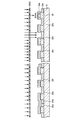
- FIG. 1 is a schematic cross-sectional view of a liquid crystal panel including a color filter according to Embodiment 1 of the present invention
- FIG. 2 is an enlarged plan view of a part of the color filter shown in FIG. 1 is a schematic cross-sectional view of the liquid crystal panel cut along the line II shown in FIG.
- the color filter in the present embodiment includes, in parallel, each pixel 28 with three colored belt-like colored layers of a red colored layer 23a, a green colored layer 23b, and a blue colored layer 23c. It is made. Therefore, the color filter in the present embodiment includes three light transmissive colored layer groups each including a red light transmissive colored layer group, a green light transmissive colored layer group, and a blue light transmissive colored layer group. Is provided.
- the liquid crystal panel 1A including the color filter in the present embodiment is sealed between the TFT substrate 10, the CF substrate 20A, and the TFT substrate 10 and the CF substrate 20A.
- the liquid crystal 18 is mainly provided.
- the TFT substrate 10 is also called an active matrix substrate, and mainly includes a transparent substrate 11, a TFT circuit layer 12, an insulating layer 13, a pixel electrode 14, and an alignment film 15.
- the transparent substrate 11 has optical transparency, and is composed of, for example, a plate-like glass substrate or a plastic substrate.
- the TFT circuit layer 12 is provided on the main surface of the transparent substrate 11 corresponding to the colored layers 23a, 23b, and 23c included in each pixel 28, and has a circuit configured by TFTs, wirings, and the like. .
- the TFT is made of, for example, amorphous silicon or polysilicon, and the wiring is made of, for example, aluminum (Al), copper (Cu), tantalum (Ta), titanium (Ti), or an alloy thereof.
- the insulating layer 13 is provided on the main surface of the transparent substrate 11 so as to cover the TFT circuit layer 12.
- a silicon compound such as silicon nitride (SiNx) or silicon oxide (SiOx), or a polyimide resin or an acrylic resin is used. It is comprised with resin materials, such as resin.
- the pixel electrode 14 is provided on the insulating layer 13 corresponding to the colored layers 23a, 23b, and 23c included in each pixel 28, and is electrically connected to the TFT circuit layer 12 described above.
- the pixel electrode 14 is composed of a transparent electrode film such as an ITO (Indium Thin Oxide) film (that is, a mixed film of indium oxide (In 2 O 3 ) and tin oxide (SnO 2 )).
- the alignment film 15 is provided on the insulating layer 13 so as to cover the pixel electrode 14, and is made of a resin material such as polyimide resin.
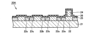
- the CF substrate 20A also called a counter substrate, corresponds to a color filter, and includes a transparent substrate 21, a black matrix layer 22, a red colored layer 23a, a green colored layer 23b, and a blue color provided corresponding to each pixel.
- the colored layer 23c is composed of three colored layers having different colors, a spacer layer 24, a counter electrode 25, and an alignment film 26.
- the transparent substrate 21 corresponds to a light-transmitting base material, and is composed of, for example, a plate-like glass substrate or a plastic substrate.
- the black matrix layer 22 corresponds to a light shielding layer and is provided on the main surface of the transparent substrate 21.
- the three colored layers 23a, 23b, and 23c having different colors are respectively provided on the main surface of the transparent substrate 21 where the black matrix layer 22 is not formed.
- the black matrix layer 22 is provided at a boundary portion between the individual colored layers 23a, 23b, and 23c, and is formed in a lattice shape by having a plurality of openings.
- the plurality of opening groups provided in the black matrix layer 22 include first openings 22a, 22b, and third openings 22c provided corresponding to the respective pixels 28, respectively.
- a group of three openings consisting of a group of parts, a second group of openings, and a group of third openings, and the above-mentioned red light-transmitting colored layer group is contained in the second group of openings.
- the green light-transmitting colored layer group described above is provided inside, and the blue light-transmitting colored layer group described above is provided in the third opening group.
- the black matrix layer 22 is formed by a photolithography method, for example, a low-reflection metal film made of chromium (Cr), molybdenum (Mo), or the like, or black photosensitive material obtained by dispersing carbon fine particles in a photosensitive resin.
- a synthetic resin film made of resin or the like is used.
- the red colored layer 23a is formed by an ink jet method using red ink, and is composed of, for example, a thermosetting resin film in which a red pigment is dispersed.
- the green colored layer 23b is formed by an inkjet method using a green ink, and is composed of, for example, a thermosetting resin film in which a green pigment is dispersed.
- the blue colored layer 23c is formed by a photolithography method, and is formed of, for example, a photosensitive resin film in which a blue pigment is dispersed.
- the spacer layer 24 is provided on a predetermined portion of the black matrix layer 22.
- the spacer layer 24 is for forming a predetermined gap between the TFT substrate 10 and the CF substrate 20A, and a plurality of the spacer layers 24 are provided on the surface of the color filter.
- the spacer layer 24 is formed by a photolithography method. For example, similarly to the black matrix layer 22, carbon fine particles are dispersed in a low reflection metal film made of chromium (Cr), molybdenum (Mo), or the like, or a photosensitive resin. And a synthetic resin film made of black photosensitive resin or the like.
- the counter electrode 25 is provided so as to cover the black matrix layer 22, the red colored layer 23a, the green colored layer 23b, the blue colored layer 23c, and the spacer layer 24 described above.
- the counter electrode 25 is composed of a transparent electrode film such as an ITO film.
- the alignment film 26 is provided on the counter electrode 25 and is made of, for example, a resin material such as polyimide resin.
- the liquid crystal 18 is sealed between the TFT substrate 10 and the CF substrate 20A.
- the liquid crystal 18 has a property of changing the light transmittance according to the applied voltage.
- the liquid crystal 18 includes the pixel electrode 14 provided on the TFT substrate 10 described above, and the counter electrode 25 provided on the CF substrate 20A described above. Located between. Note that polarizing plates (not shown) are attached to the main surfaces of the TFT substrate 10 and the CF substrate 20A that do not face the liquid crystal 18, respectively.
- FIG. 3 is a flowchart for explaining a method for manufacturing a color filter in the present embodiment
- FIGS. 4 to 6 are schematic diagrams in a manufacturing process when the color filter in the present embodiment is manufactured according to the flow. It is sectional drawing. Next, with reference to these FIG. 3 thru
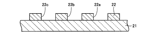
- a transparent substrate 21 as a light-transmitting base material is prepared, and a light shielding layer is formed on the transparent substrate 21 using a photolithography method.
- a black matrix layer 22 is formed (step S101).
- a black photosensitive resin layer 22p is formed by applying and drying a black photosensitive resin liquid on the main surface of the transparent substrate 21 using, for example, a spin coating method.
- the black photosensitive resin layer 22p is exposed using a photomask 31A having a predetermined opening shape, and thereafter development is performed using a predetermined etching solution.
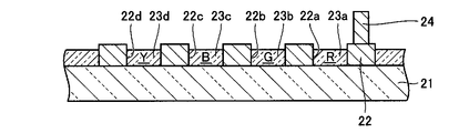
- a black matrix layer 22 having a first opening 22a, a second opening 22b, and a third opening 22c is formed on the transparent substrate 21 as shown in FIG. 4B.
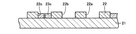
- a blue light-transmitting colored layer group is formed on the transparent substrate 21 using a photolithography method (step S102). Specifically, as shown in FIG. 4C, a blue photosensitive resin liquid is applied over the entire main surface of the transparent substrate 21 on which the black matrix layer 22 is formed using, for example, a spin coat method and dried. Thus, the blue photosensitive resin layer 23p is formed, and then the blue photosensitive resin layer 23p is exposed using a photomask 32A having a predetermined opening shape, and then developed using a predetermined etching solution. It is. As a result, a blue colored layer 23c is formed in the third opening 22c of the black matrix layer 22 as shown in FIG. 4D.
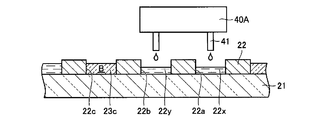
- a red light-transmitting colored layer group and a green light-transmitting colored layer group are respectively formed on the transparent substrate 21 using an ink jet method (step S103).
- the red ink 23x is provided on the transparent substrate 21 where the first opening 22a of the black matrix layer 22 is provided, and the second opening 22b of the black matrix layer 22 is provided.
- a predetermined amount of the green ink 23y is dropped on the transparent substrate 21 in the portion using the nozzle 41 provided in the ink jet head 40A, and then is cured by being heated.
- FIG. 5B a red colored layer 23a is formed in the first opening 22a of the black matrix layer 22, and a green colored layer 23b is formed in the second opening 22b of the black matrix layer 22, respectively. .
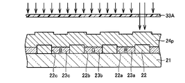
- a spacer layer group is formed on a predetermined portion of the black matrix layer 22 using a photolithography method (step S104).
- a photolithography method for example, spin coating is entirely applied on the black matrix layer 22, the red light-transmitting colored layer group, the green light-transmitting colored layer group, and the blue light-transmitting colored layer group.
- the black photosensitive resin liquid 24p is formed by applying and drying the black photosensitive resin liquid using the method, and then using the photomask 33A having a predetermined opening shape, the black photosensitive resin layer 24p is formed. Exposure is performed, and then development is performed using a predetermined etching solution. As a result, a spacer layer 24 as shown in FIG. 5D is formed on a predetermined portion of the black matrix layer 22.
- an ITO film is formed using, for example, a sputtering method so as to cover the black matrix layer 22, the red light transmissive colored layer group, the green light transmissive colored layer group, the blue light transmissive colored layer group, and the spacer layer group. Is formed, and a counter electrode 25 is formed. Further, a polyimide resin is applied on the counter electrode 25 by using, for example, a spin coating method and dried, whereby the alignment film 26 is formed. Thus, the manufacture of the CF substrate 20A (color filter) as shown in FIG. 6 is completed.
- the black matrix layer is formed using a photolithography method
- the blue light-transmitting colored layer group is formed using a photolithography method
- the red light-transmitting property is formed.
- a colored layer group and a green light-transmitting colored layer group are formed using an ink jet method. Therefore, by forming the black matrix layer using a photolithography method, the black matrix layer can be formed with higher accuracy, and a blue light-transmitting colored layer group is formed using a photolithography method. By doing so, it is possible to abolish the formation by the ink jet method using the blue ink, which is difficult to prepare compared with the inks of other colors, so that the blue light-transmitting colored layer group can be formed more easily. become.
- the red light-transmitting colored layer group and the green light-transmitting colored layer group using the inkjet method, it is possible to form these colored layer groups at the same time and more easily The light-transmitting colored layer group and the green light-transmitting colored layer group can be formed. For this reason, it is possible to manufacture a color filter by taking advantage of the advantages of the photolithography method and the ink jet method as compared with the prior art.
- the black matrix layer is formed at the boundary portion of the colored layer, the black matrix layer is used to form a gap between the pixels or a region where the TFT is formed. The incident light can be prevented. Therefore, by using the liquid crystal panel including the color filter in this embodiment, a liquid crystal panel capable of high-quality display can be obtained.
- a liquid crystal panel capable of high-quality display can be manufactured at low cost by taking advantage of the advantages of the photolithography method and the inkjet method. Panels can be manufactured at low cost.
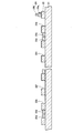
- FIG. 7 is a schematic cross-sectional view of a liquid crystal panel including the color filter according to Embodiment 2 of the present invention
- FIG. 8 is an enlarged plan view of a part of the color filter shown in FIG.
- FIG. 7 is a schematic cross-sectional view when the liquid crystal panel is cut along the line VII-VII shown in FIG.
- the structure of the color filter in this Embodiment and the liquid crystal panel provided with the said color filter is demonstrated in detail.
- the same parts as those in the first embodiment are given the same reference numerals in the figure, and the description thereof will not be repeated here.
- each pixel 28 has a four-color belt-like coloring of a red colored layer 23a, a green colored layer 23b, a blue colored layer 23c, and a yellow colored layer 23d.
- the color filter in the present embodiment includes a red light-transmitting colored layer group, a green light-transmitting colored layer group, a blue light-transmitting colored layer group, and a yellow light-transmitting colored layer group. It comprises four light transmissive colored layer groups.
- the liquid crystal panel 1B having the color filter in the present embodiment is sealed between the TFT substrate 10, the CF substrate 20B, and the TFT substrate 10 and the CF substrate 20B.
- the liquid crystal 18 is mainly provided.
- the liquid crystal panel 1B including the color filter in the present embodiment differs from the liquid crystal panel 1A in the first embodiment described above only in the configuration of the CF substrate.
- the CF substrate 20B corresponds to a color filter, and includes a transparent substrate 21, a black matrix layer 22, a red colored layer 23a, a green colored layer 23b, a blue colored layer 23c, and a yellow color layer provided for each pixel.
- the colored layer 23d is composed of four colored layers having different colors, a spacer layer 24, a counter electrode 25, and an alignment film 26.
- the transparent substrate 21 corresponds to a light-transmitting base material, and is composed of, for example, a plate-like glass substrate or a plastic substrate.
- the black matrix layer 22 corresponds to a light shielding layer and is provided on the main surface of the transparent substrate 21.
- the four colored layers 23a, 23b, 23c, and 23d having different colors are provided on the main surface of the transparent substrate 21 where the black matrix layer 22 is not formed.
- the black matrix layer 22 is provided at a boundary portion between the individual colored layers 23a, 23b, 23c, and 23d, and is formed in a lattice shape by having a plurality of openings.
- the plurality of opening groups provided in the black matrix layer 22 include a first opening 22a, a second opening 22b, a third opening 22c, and a fourth opening 22d provided corresponding to each pixel 28.
- the transparent colored layer group includes the green light-transmitting colored layer group described above in the second opening group, and the blue light-transmitting colored layer group described above in the third opening group.
- Each of the yellow colored layers described above is provided therein.
- the black matrix layer 22 is formed by a photolithography method, for example, a low-reflection metal film made of chromium (Cr), molybdenum (Mo), or the like, or black photosensitive material obtained by dispersing carbon fine particles in a photosensitive resin.
- a synthetic resin film made of resin or the like is used.
- the red colored layer 23a is formed by an ink jet method using red ink, and is composed of, for example, a thermosetting resin film in which a red pigment is dispersed.
- the green colored layer 23b is formed by an inkjet method using a green ink, and is composed of, for example, a thermosetting resin film in which a green pigment is dispersed.
- the blue colored layer 23c is formed by an ink jet method using a blue ink, and is composed of, for example, a thermosetting resin film in which a blue pigment is dispersed.
- the yellow colored layer 23d is formed by a photolithography method, and is composed of, for example, a photosensitive resin film in which a yellow pigment is dispersed.
- the spacer layer 24 is provided on a predetermined portion of the black matrix layer 22.
- the spacer layer 24 is for forming a predetermined gap between the TFT substrate 10 and the CF substrate 20B, and a plurality of spacer layers 24 are provided on the surface of the color filter.
- the spacer layer 24 is formed by a photolithography method.
- carbon fine particles are dispersed in a low reflection metal film made of chromium (Cr), molybdenum (Mo), or the like, or a photosensitive resin.
- a synthetic resin film made of black photosensitive resin or the like.
- the counter electrode 25 is provided so as to cover the black matrix layer 22, the red colored layer 23a, the green colored layer 23b, the blue colored layer 23c, the yellow colored layer 23d, and the spacer layer 24 described above.
- the counter electrode 25 is composed of a transparent electrode film such as an ITO film.
- the alignment film 26 is provided on the counter electrode 25 and is made of, for example, a resin material such as polyimide resin.
- FIG. 9 is a flowchart for explaining a method for manufacturing a color filter in the present embodiment
- FIGS. 10 to 12 are schematic diagrams in a manufacturing process when the color filter in the present embodiment is manufactured according to the flow. It is sectional drawing. Next, with reference to FIGS. 9 to 12, a method for manufacturing a color filter in the present embodiment will be described in detail.
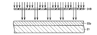
- a transparent substrate 21 as a light-transmitting base material is prepared, and a light shielding layer is formed on the transparent substrate 21 using a photolithography method.
- a black matrix layer 22 is formed (step S201).
- a black photosensitive resin layer 22p is formed by applying and drying a black photosensitive resin liquid on the main surface of the transparent substrate 21 using, for example, a spin coating method.
- the black photosensitive resin layer 22p is exposed using a photomask 31B having a predetermined opening shape, and thereafter development is performed using a predetermined etching solution.
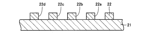
- the black matrix layer 22 having the first opening 22a, the second opening 22b, the third opening 22c, and the fourth opening 22d is formed on the transparent substrate 21.
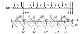
- a yellow light-transmitting colored layer group is formed on the transparent substrate 21 by using a photolithography method (step S202). Specifically, as shown in FIG. 10C, a yellow photosensitive resin liquid is applied over the entire main surface of the transparent substrate 21 on which the black matrix layer 22 is formed using, for example, a spin coating method and dried. As a result, the yellow photosensitive resin layer 23q is formed, and then the yellow photosensitive resin layer 23q is exposed using a photomask 32B having a predetermined opening shape, and then development is performed using a predetermined etching solution. It is. As a result, a yellow colored layer 23d is formed in the fourth opening 22d of the black matrix layer 22 as shown in FIG. 10D.
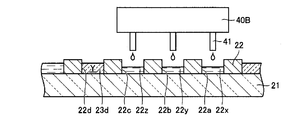
- a red light-transmitting colored layer group, a green light-transmitting colored layer group, and a blue light-transmitting colored layer group are formed on the transparent substrate 21 using the ink jet method.
- Step S203 Specifically, as shown in FIG. 11A, the red ink 23x is provided on the transparent substrate 21 where the first opening 22a of the black matrix layer 22 is provided, and the second opening 22b of the black matrix layer 22 is provided.
- the nozzle 41 provided on the inkjet head 40B is the green ink 23y on the transparent substrate 21 in the portion thus formed and the blue ink 23z on the transparent substrate 21 in the portion where the third opening 22c of the black matrix layer 22 is provided.
- a predetermined amount is dripped using, and is then cured by heating. Accordingly, as shown in FIG. 11B, the red colored layer 23a is formed in the first opening 22a of the black matrix layer 22, the green colored layer 23b is formed in the second opening 22b of the black matrix layer 22, and the black matrix layer 22 is formed. A blue colored layer 23c is formed in each of the third openings 22c.
- a spacer layer group is formed on a predetermined portion of the black matrix layer 22 by using a photolithography method (step S204).
- a black matrix layer 22 a red light-transmitting colored layer group, a green light-transmitting colored layer group, a blue light-transmitting colored layer group, and a yellow light-transmitting coloring
- a black photosensitive resin liquid 24p is formed by applying a black photosensitive resin liquid over the entire layer group using, for example, a spin coating method and drying, and then a photomask 33B having a predetermined opening shape is formed. Then, the black photosensitive resin layer 24p is exposed to light and then developed using a predetermined etching solution. As a result, a spacer layer 24 as shown in FIG. 11D is formed on a predetermined portion of the black matrix layer 22.
- the black matrix layer 22, the red light-transmitting colored layer group, the green light-transmitting colored layer group, the blue light-transmitting colored layer group, the yellow light-transmitting colored layer group, and the spacer layer group are covered.
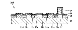
- the counter electrode 25 is formed by forming an ITO film using, for example, a sputtering method, and further, a polyimide resin is applied on the counter electrode 25 using, for example, a spin coating method and dried to obtain an alignment film. 26 is formed.
- the manufacture of the CF substrate 20B (color filter) as shown in FIG. 12 is completed.
- the black matrix layer is formed using the photolithography method
- the yellow light-transmitting colored layer group is formed using the photolithography method
- the red light-transmitting property is formed.
- a colored layer group, a green light-transmitting colored layer group, and a blue light-transmitting colored layer group are formed using an inkjet method. Therefore, by forming the black matrix layer using a photolithography method, the black matrix layer can be formed with higher accuracy, and a yellow light-transmitting colored layer group is formed using a photolithography method.
- the black matrix layer is formed at the boundary portion of the colored layer, the black matrix layer is used to form a gap between the pixels or a region where the TFT is formed. The incident light can be prevented. Therefore, by using the liquid crystal panel including the color filter in this embodiment, a liquid crystal panel capable of high-quality display can be obtained.
- a liquid crystal panel capable of high-quality display can be manufactured at low cost by taking advantage of the advantages of the photolithography method and the inkjet method. Panels can be manufactured at low cost.
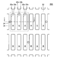
- FIG. 13 is an enlarged plan view of a part of a color filter according to another example of the present embodiment. As shown in FIG.
- the above-described four colored layers 23a, 23b, 23c, and 23d are formed in a rectangular shape, and the four A layout in which the colored layers 23a, 23b, 23c, and 23d are alternately arranged along the matrix direction may be employed.
- each pixel 28 is provided with four colored layers of a red colored layer 23a, a green colored layer 23b, a blue colored layer 23c, and a yellow colored layer 23d.
- a colored layer of another color for example, white
- the colored layers of the other colors must be formed by a photolithography method.
- red light transmissive colored layer group a green light transmissive colored layer group, a blue light transmissive colored layer group, and a yellow light transmissive colored layer group.
- the red light-transmitting colored layer group, the light-transmitting colored layer group, and the blue light-transmitting colored layer group are formed by photolithography.
- One or two light transmissive colored layer groups selected from among them may be formed by photolithography.
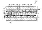
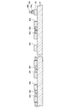
- FIG. 14 is a schematic cross-sectional view of a liquid crystal panel including the color filter according to Embodiment 3 of the present invention
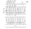
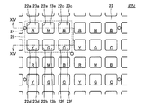
- FIG. 15 is an enlarged plan view of a part of the color filter shown in FIG.
- FIG. 14 is a schematic cross-sectional view of the liquid crystal panel cut along the line XIV-XIV shown in FIG.
- the color filter in the present embodiment includes a red colored layer 23a, a green colored layer 23b, a blue colored layer 23c, a yellow colored layer 23d, and a magenta colored layer 23e in each pixel 28.
- six colored rectangular colored layers of cyan colored layer 23f are alternately provided along the matrix direction. Therefore, the color filter in the present embodiment includes a red light-transmitting colored layer group, a green light-transmitting colored layer group, a blue light-transmitting colored layer group, and a yellow light-transmitting colored layer group.
- six light transmissive colored layer groups each including a magenta light transmissive colored layer group and a cyan light transmissive colored layer group.
- the liquid crystal panel 1C having the color filter in the present embodiment is sealed between the TFT substrate 10, the CF substrate 20C, and the TFT substrate 10 and the CF substrate 20C.
- the liquid crystal 18 is mainly provided.
- the liquid crystal panel 1C including the color filter in the present embodiment is different from the liquid crystal panel 1A in the first embodiment described above only in the configuration of the CF substrate.
- the CF substrate 20C corresponds to a color filter, and includes a transparent substrate 21, a black matrix layer 22, a red colored layer 23a, a green colored layer 23b, a blue colored layer 23c, and a yellow color layer provided corresponding to each pixel.
- the transparent substrate 21 corresponds to a light-transmitting base material, and is composed of, for example, a plate-like glass substrate or a plastic substrate.
- the black matrix layer 22 corresponds to a light shielding layer and is provided on the main surface of the transparent substrate 21.
- Six colored layers 23a, 23b, 23c, 23d, 23e, and 23f having different colors are respectively provided on the main surface of the transparent substrate 21 where the black matrix layer 22 is not formed.
- the black matrix layer 22 is provided at the boundary between the individual colored layers 23a, 23b, 23c, 23d, 23e, and 23f, and is formed in a lattice shape by having a plurality of opening groups.
- the plurality of opening groups provided in the black matrix layer 22 include a first opening 22a, a second opening 22b, a third opening 22c, and a fourth opening 22d provided corresponding to each pixel 28.
- a first opening group, a second opening group, a third opening group, a fourth opening group, a fifth opening group, and a sixth opening group each including a fifth opening 22e and a sixth opening 22f.
- the black matrix layer 22 is formed by a photolithography method, for example, a low-reflection metal film made of chromium (Cr), molybdenum (Mo), or the like, or black photosensitive material obtained by dispersing carbon fine particles in a photosensitive resin.
- a synthetic resin film made of resin or the like is used.
- the red colored layer 23a is formed by an ink jet method using red ink, and is composed of, for example, a thermosetting resin film in which a red pigment is dispersed.
- the green colored layer 23b is formed by an inkjet method using a green ink, and is composed of, for example, a thermosetting resin film in which a green pigment is dispersed.
- the blue colored layer 23c is formed by an ink jet method using a blue ink, and is composed of, for example, a thermosetting resin film in which a blue pigment is dispersed.
- the yellow colored layer 23d is formed by a photolithography method, and is composed of, for example, a photosensitive resin film in which a yellow pigment is dispersed.
- the magenta colored layer 23e is formed by a photolithography method, and is formed of, for example, a photosensitive resin film in which a magenta pigment is dispersed.
- the cyan colored layer 23f is formed by a photolithography method, and is formed of, for example, a photosensitive resin film in which a magenta pigment is dispersed.
- the spacer layer 24 is provided on a predetermined portion of the black matrix layer 22.
- the spacer layer 24 is for forming a predetermined gap between the TFT substrate 10 and the CF substrate 20B, and a plurality of spacer layers 24 are provided on the surface of the color filter.
- the spacer layer 24 has a first spacer layer 24a and a second spacer layer 24b stacked in the thickness direction.
- the first spacer layer 24a is formed by a photolithography method, and is composed of, for example, a photosensitive resin film in which a yellow pigment is dispersed, like the yellow colored layer 23d.
- the second spacer layer 24b is formed by a photolithography method, and is formed of a photosensitive resin film in which, for example, a magenta color pigment is dispersed, like the magenta color layer 23e.
- the counter electrode 25 includes the above-described black matrix layer 22, red colored layer 23a, green colored layer 23b, blue colored layer 23c, yellow colored layer 23d, magenta colored layer 23e, cyan colored layer 23f and The spacer layer 24 is provided so as to cover it.
- the counter electrode 25 is composed of a transparent electrode film such as an ITO film.
- the alignment film 26 is provided on the counter electrode 25 and is made of, for example, a resin material such as polyimide resin.
- FIG. 16 is a flowchart for explaining a method of manufacturing a color filter in the present embodiment
- FIGS. 17 to 22 are schematic diagrams in a manufacturing process when the color filter in the present embodiment is manufactured according to the flow. It is sectional drawing. Next, with reference to FIGS. 16 to 22, a method for manufacturing a color filter in the present embodiment will be described in detail.
- a transparent substrate 21 as a light-transmitting base material is prepared, and a light shielding layer is formed on the transparent substrate 21 using a photolithography method.
- the black matrix layer 22 is formed (step S301).
- a black photosensitive resin layer 22p is formed by applying and drying a black photosensitive resin liquid on the main surface of the transparent substrate 21 using, for example, a spin coating method.
- the black photosensitive resin layer 22p is exposed using a photomask 31C having a predetermined opening shape, and then developed using a predetermined etching solution.
- FIG. 17B the black matrix layer 22 having the first opening 22a, the second opening 22b, the third opening 22c, the fourth opening 22d, the fifth opening 22e, and the sixth opening 22f is formed. It is formed on the transparent substrate 21.
- a yellow light-transmitting colored layer group and a first spacer layer group are formed on the transparent substrate 21 using a photolithography method (step S302).
- a yellow photosensitive resin liquid is applied over the entire main surface of the transparent substrate 21 on which the black matrix layer 22 is formed by using, for example, a spin coating method and dried.
- a yellow photosensitive resin layer 23q is formed, and then the yellow photosensitive resin layer 23q is exposed using a photomask 32B1 having a predetermined opening shape, and then developed using a predetermined etching solution. It is.
- a yellow colored layer 23 d is formed in the fourth opening 22 d of the black matrix layer 22, and a first spacer layer 24 a is formed on a predetermined portion of the black matrix layer 22.
- a magenta light-transmitting colored layer group and a second spacer layer group are formed on the transparent substrate 21 using a photolithography method (step S303).
- a magenta photosensitive resin solution is formed on the entire main surface of the transparent substrate 21 on which the black matrix layer 22 and the yellow colored layer 23d are formed by using, for example, a spin coating method. Is applied and dried to form a magenta photosensitive resin layer 23r, followed by exposure of the magenta photosensitive resin layer 23r using a photomask 32B2 having a predetermined opening shape. Development is performed using this etching solution.
- a magenta colored layer 23e is formed in the fifth opening 22e of the black matrix layer 22, and a second spacer layer 24b is formed on the first spacer layer 24a.
- a cyan light-transmitting colored layer group is formed on the transparent substrate 21 by using a photolithography method (step S304). Specifically, as shown in FIG. 20A, the entire surface of the transparent substrate 21 on which the black matrix layer 22, the yellow colored layer 23d, and the magenta colored layer 23e are formed, for example, using a spin coat method.
- a cyan photosensitive resin layer 23s is formed by applying and drying a cyan photosensitive resin liquid, and then exposing the cyan photosensitive resin layer 23s using a photomask 32B3 having a predetermined opening shape. Then, development is performed using a predetermined etching solution. As a result, a cyan colored layer 23f is formed in the sixth opening 22f of the black matrix layer 22 as shown in FIG. 20B.
- a red light-transmitting colored layer group, a green light-transmitting colored layer group, and a blue light-transmitting colored layer group are formed on the transparent substrate 21 using an inkjet method.
- Step S305 Specifically, as shown in FIG. 21A, the red ink 22x is provided on the transparent substrate 21 where the first opening 22a of the black matrix layer 22 is provided, and the second opening 22b of the black matrix layer 22 is provided.
- the nozzle 41 provided on the inkjet head 40C is the green ink 22y on the portion of the transparent substrate 21 where the ink is applied, and the blue ink 22z is on the transparent substrate 21 where the third opening 22d of the black matrix layer 22 is provided.
- a predetermined amount is dripped using, and is then cured by heating. Accordingly, as shown in FIG. 21B, the red colored layer 23a is formed in the first opening 22a of the black matrix layer 22, the green colored layer 23b is formed in the second opening 22b of the black matrix layer 22, and the black matrix layer 22 is formed. A blue colored layer 23c is formed in each of the third openings 22c.
- the counter electrode 25 is formed by depositing an ITO film, for example, using a sputtering method so as to cover the cyan colored layer group and the spacer layer group. Further, for example, a spin coat method is used on the counter electrode 25. Then, the alignment film 26 is formed by applying and drying the polyimide resin. Thus, the manufacture of the CF substrate 20C (color filter) as shown in FIG. 22 is completed.
- the black matrix layer is formed using a photolithography method, and the yellow light-transmitting colored layer group, the magenta light-transmitting colored layer group, and the cyan light
- a transparent colored layer group is formed using a photolithography method, and a red light transmitting colored layer group, a green light transmitting colored layer group, and a blue light transmitting colored layer group are formed using an inkjet method. Yes. Therefore, by forming the black matrix layer using a photolithography method, the black matrix layer can be formed with higher accuracy, and the yellow light-transmitting coloring layer group and the magenta light-transmitting coloring can be formed.
- yellow, magenta, and cyan inks which are difficult to prepare compared to other color inks, by forming each layer group and cyan light-transmissive colored layer group using photolithography.
- the formation by yellow ink-jet method can be abolished so that yellow light-transmitting colored layer groups, magenta light-transmitting colored layer groups, and cyan light-transmitting colored layer groups can be formed more easily.
- by forming the red light-transmitting colored layer group, the green light-transmitting colored layer group, and the blue light-transmitting colored layer group using the inkjet method these colored layer groups can be formed simultaneously.
- a color filter can be manufactured taking advantage of the advantages of the photolithography method and the inkjet method.
- the black matrix layer is formed at the boundary portion of the colored layer, the black matrix layer is used to form a gap between the pixels or a region where the TFT is formed. The incident light can be prevented. Therefore, by using the liquid crystal panel including the color filter in this embodiment, a liquid crystal panel capable of high-quality display can be obtained.
- a liquid crystal panel capable of high-quality display can be manufactured at low cost by taking advantage of the advantages of the photolithography method and the inkjet method. Panels can be manufactured at low cost.
- the red colored layer 23a, the green colored layer 23b, the blue colored layer 23c, the yellow colored layer 23d, the magenta colored layer 23e, and the cyan colored layer 23f are used.
- these six colored layers are not necessarily rectangular and arranged in the matrix direction. It is not necessary to be formed alternately.
- a layout in which the above-described six colored layers 23a, 23b, 23c, 23d, 23e, and 23f are each formed in a strip shape and are arranged in parallel may be adopted.
- the red light-transmitting colored layer group, the green light-transmitting colored layer group, the blue light-transmitting colored layer group, the yellow light-transmitting colored layer group, and the magenta color The description has been made by exemplifying the color filter including the six light transmissive colored layer groups of the light transmissive colored layer group and the cyan light transmissive colored layer group.
- the combination of colors may be any combination, and the number of light-transmitting colored layer groups formed is not limited to six colors.
- the above-described effects can be obtained if a plurality of light-transmitting colored layer groups are provided, part of which is formed using a photolithography method and the remaining part is formed using an inkjet method. become.
- three light-transmitting colored layer groups are formed by an inkjet method, and the remaining one or three light-transmitting colored layer groups are formed by a photolithography method.
- the case has been described by way of example, and thus three light-transmitting colored layer groups selected from four or more light-transmitting colored layer groups having different colors are formed by the inkjet method and remain.
- existing production facilities can be used efficiently. This is because existing production facilities often use so-called three-color inkjet devices corresponding to the three colors of red, green, and blue, and the light transmission formed by the inkjet method.
- the inkjet apparatus cannot be used efficiently. Therefore, by adopting as in the second and third embodiments described above, the existing ink jet apparatus can be efficiently utilized as it is, and an increase in manufacturing cost can be suppressed.
- 1A, 1B, 1C liquid crystal panel 10 TFT substrate, 11 transparent substrate, 12 TFT circuit layer, 13 insulating layer, 14 pixel electrode, 15 alignment film, 18 liquid crystal, 20A, 20B, 20C CF substrate, 21 transparent substrate, 22 black Matrix layer, 22a 1st opening, 22b 2nd opening, 22c 3rd opening, 22d 4th opening, 22e 5th opening, 22f 6th opening, 22p black photosensitive resin layer, 23a red coloring Layer, 23b green colored layer, 23c blue colored layer, 23d yellow colored layer, 23e magenta colored layer, 23f cyan colored layer, 23p blue photosensitive resin layer, 23q yellow photosensitive resin layer, 23r magenta Color photosensitive resin layer, 23s cyan photosensitive resin layer, 23x red ink, 23y green ink, 23 Blue ink, 24 spacer layer, 24a 1st spacer layer, 24b 2nd spacer layer, 24p black photosensitive resin layer, 25 counter electrode, 26 alignment film, 28 pixels, 31A, 31B, 31
Landscapes
- Physics & Mathematics (AREA)
- General Physics & Mathematics (AREA)
- Nonlinear Science (AREA)
- Optics & Photonics (AREA)
- Engineering & Computer Science (AREA)
- Manufacturing & Machinery (AREA)
- Mathematical Physics (AREA)
- Chemical & Material Sciences (AREA)
- Crystallography & Structural Chemistry (AREA)
- Optical Filters (AREA)
- Liquid Crystal (AREA)
Abstract
Description
(a)上記基材上に複数の開口部群を含む遮光層をフォトリソグラフィ法にて形成する工程。
(b)上記複数の開口部群のうちから選択される一の開口部群内に、上記複数の光透過性着色層群のうちから選択される一の光透過性着色層群をフォトリソグラフィ法にて形成する工程。
(c)上記複数の開口部群のうちから選択される他の一の開口部群内に、上記複数の光透過性着色層群のうちから選択される他の一の光透過性着色層群をインクジェット法にて形成する工程。
図1は、本発明の実施の形態1におけるカラーフィルタを具備してなる液晶パネルの模式断面図であり、図2は、図1に示すカラーフィルタの一部分を拡大した平面図である。なお、図1は、図2に示すI-I線に沿って液晶パネルを切断した場合の模式断面図である。まず、これら図1および図2を参照して、本実施の形態におけるカラーフィルタならびに当該カラーフィルタを具備してなる液晶パネルの構造について詳細に説明する。
図7は、本発明の実施の形態2におけるカラーフィルタを具備してなる液晶パネルの模式断面図であり、図8は、図7に示すカラーフィルタの一部分を拡大した平面図である。なお、図7は、図8に示すVII-VII線に沿って液晶パネルを切断した場合の模式断面図である。まず、これら図7および図8を参照して、本実施の形態におけるカラーフィルタならびに当該カラーフィルタを具備してなる液晶パネルの構造について詳細に説明する。なお、上述の実施の形態1と同様の部分については図中同一の符号を付し、その説明はここでは繰り返さない。
図14は、本発明の実施の形態3におけるカラーフィルタを具備してなる液晶パネルの模式断面図であり、図15は、図14に示すカラーフィルタの一部分を拡大した平面図である。なお、図14は、図15に示すXIV-XIV線に沿って液晶パネルを切断した場合の模式断面図である。まず、これら図14および図15を参照して、本実施の形態におけるカラーフィルタならびに当該カラーフィルタを具備してなる液晶パネルの構造について詳細に説明する。なお、上述の実施の形態1と同様の部分については図中同一の符号を付し、その説明はここでは繰り返さない。
Claims (17)
- 光透過性の基材(21)上に色の異なる複数の光透過性着色層群を備えてなるカラーフィルタの製造方法であって、
前記基材(21)上に複数の開口部群を含む遮光層をフォトリソグラフィ法にて形成する工程と、
前記複数の開口部群のうちから選択される一の開口部群内に、前記複数の光透過性着色層群のうちから選択される一の光透過性着色層群をフォトリソグラフィ法にて形成する工程と、
前記複数の開口部群のうちから選択される他の一の開口部群内に、前記複数の光透過性着色層群のうちから選択される他の一の光透過性着色層群をインクジェット法にて形成する工程とを備えた、カラーフィルタの製造方法。 - 前記一の光透過性着色層群をフォトリソグラフィ法にて形成する工程が、前記他の一の光透過性着色層群をインクジェット法にて形成する工程よりも先に行なわれる、請求の範囲第1項に記載のカラーフィルタの製造方法。
- 前記他の一の光透過性着色層群をインクジェット法にて形成する工程が、前記一の光透過性着色層群をフォトリソグラフィ法にて形成する工程よりも先に行なわれる、請求の範囲第1項に記載のカラーフィルタの製造方法。
- 前記一の光透過性着色層群をフォトリソグラフィ法にて形成する工程において、前記遮光層の所定部位上に突出して位置するスペーサ層群を前記一の光透過性着色層群とともに同時に形成する、請求の範囲第1項から第3項のいずれかに記載のカラーフィルタの製造方法。
- 前記複数の光透過性着色層群が、少なくとも色の異なる4つ以上の光透過性着色層群にて構成され、
これら4つ以上の光透過性着色層群のうちから選択される3つの光透過性着色層群がインクジェット法にて形成され、残る光透過性着色層群がフォトリソグラフィ法にて形成される、請求の範囲第1項から第4項のいずれかに記載のカラーフィルタの製造方法。 - 前記複数の光透過性着色層群が、赤色の光透過性着色層(23a)群、緑色の光透過性着色層(23b)群および青色の光透過性着色層(23c)群からなる3つの光透過性着色層群にて構成され、
これら3つの光透過性着色層群のうちから選択される少なくとも1つの光透過性着色層群がフォトリソグラフィ法にて形成され、残る光透過性着色層群がインクジェット法にて形成される、請求の範囲第1項から第4項のいずれかに記載のカラーフィルタの製造方法。 - 前記複数の光透過性着色層群が、赤色の光透過性着色層(23a)群、緑色の光透過性着色層(23b)群、青色の光透過性着色層(23c)群および黄色の光透過性着色層(23d)群からなる4つの光透過性着色層群にて構成され、
これら4つの光透過性着色層群のうちから選択される少なくとも1つの光透過性着色層群がフォトリソグラフィ法にて形成され、残る光透過性着色層群がインクジェット法にて形成される、請求の範囲第1項から第4項のいずれかに記載のカラーフィルタの製造方法。 - 前記複数の光透過性着色層群が、赤色の光透過性着色層(23a)群、緑色の光透過性着色層(23b)群、青色の光透過性着色層(23c)群および白色の光透過性着色層群からなる4つの光透過性着色層群にて構成され、
これら4つの光透過性着色層群のうちから選択される少なくとも1つの光透過性着色層群がフォトリソグラフィ法にて形成され、残る光透過性着色層群がインクジェット法にて形成される、請求の範囲第1項から第4項のいずれかに記載のカラーフィルタの製造方法。 - 前記複数の光透過性着色層群が、赤色の光透過性着色層(23a)群、緑色の光透過性着色層(23b)群、青色の光透過性着色層(23c)群、黄色の光透過性着色層(23d)群、マゼンタ色の光透過性着色層(23e)群およびシアン色の光透過性着色層(23f)群からなる6つの光透過性着色層群にて構成され、
これら6つの光透過性着色層群のうちから選択される少なくとも1つの光透過性着色層群がフォトリソグラフィ法にて形成され、残る光透過性着色層群がインクジェット法にて形成される、請求の範囲第1項から第4項のいずれかに記載のカラーフィルタの製造方法。 - 前記遮光層が、低反射金属膜または合成樹脂膜からなるブラックマトリクス層(22)である、請求の範囲第1項から第9項のいずれかに記載のカラーフィルタの製造方法。
- 光透過性の基材(21)と、
前記基材(21)上に設けられた複数の開口部群を含む遮光層と、
前記基材(21)上に設けられた色の異なる複数の光透過性着色層群とを備え、
前記複数の光透過性着色層群のうちから選択される一の光透過性着色層群は、前記複数の開口部群のうちから選択される一の開口部群内にフォトリソグラフィ法にて形成されており、
前記複数の光透過性着色層群のうちから選択される他の一の光透過性着色層群は、前記複数の開口部群のうちから選択される他の一の開口部群内にインクジェット法にて形成されている、カラーフィルタ。 - 前記遮光層の所定部位上に突出して位置するスペーサ層群をさらに備え、
前記一の光透過性着色層群と前記スペーサ層群とが、一の工程で同時に形成されたものである、請求の範囲第11項に記載のカラーフィルタ。 - 前記複数の光透過性着色層群が、赤色の光透過性着色層(23a)群、緑色の光透過性着色層(23b)群および青色の光透過性着色層(23c)群からなる3つの光透過性着色層群にて構成されている、請求の範囲第11項または第12項に記載のカラーフィルタ。
- 前記複数の光透過性着色層群が、赤色の光透過性着色層(23a)群、緑色の光透過性着色層(23b)群、青色の光透過性着色層(23c)群および黄色の光透過性着色層(23d)群からなる4つの光透過性着色層群にて構成されている、請求の範囲第11項または第12項に記載のカラーフィルタ。
- 前記複数の光透過性着色層群が、赤色の光透過性着色層(23a)群、緑色の光透過性着色層(23b)群、青色の光透過性着色層(23c)群および白色の光透過性着色層群からなる4つの光透過性着色層群にて構成されている、請求の範囲第11項または第12項に記載のカラーフィルタ。
- 前記複数の光透過性着色層群が、赤色の光透過性着色層(23a)群、緑色の光透過性着色層(23b)群、青色の光透過性着色層(23c)群、黄色の光透過性着色層(23d)群、マゼンタ色の光透過性着色層(23e)群およびシアン色の光透過性着色層(23f)群からなる6つの光透過性着色層群にて構成されている、請求の範囲第11項または第12項に記載のカラーフィルタ。
- 前記遮光層が、低反射金属膜または合成樹脂膜からなるブラックマトリクス層(22)である、請求の範囲第11項から第16項のいずれかに記載のカラーフィルタ。
Priority Applications (2)
| Application Number | Priority Date | Filing Date | Title |
|---|---|---|---|
| US13/377,104 US20120075737A1 (en) | 2009-06-09 | 2010-04-13 | Method of manufacturing color filter and color filter |
| CN201090000939.3U CN202600174U (zh) | 2009-06-09 | 2010-04-13 | 彩色滤光片 |
Applications Claiming Priority (2)
| Application Number | Priority Date | Filing Date | Title |
|---|---|---|---|
| JP2009138422 | 2009-06-09 | ||
| JP2009-138422 | 2009-06-09 |
Publications (1)
| Publication Number | Publication Date |
|---|---|
| WO2010143467A1 true WO2010143467A1 (ja) | 2010-12-16 |
Family
ID=43308727
Family Applications (1)
| Application Number | Title | Priority Date | Filing Date |
|---|---|---|---|
| PCT/JP2010/056575 Ceased WO2010143467A1 (ja) | 2009-06-09 | 2010-04-13 | カラーフィルタの製造方法およびカラーフィルタ |
Country Status (3)
| Country | Link |
|---|---|
| US (1) | US20120075737A1 (ja) |
| CN (1) | CN202600174U (ja) |
| WO (1) | WO2010143467A1 (ja) |
Families Citing this family (2)
| Publication number | Priority date | Publication date | Assignee | Title |
|---|---|---|---|---|
| US9645436B2 (en) * | 2014-06-17 | 2017-05-09 | Apple Inc. | Color filter structures for electronic devices with color displays |
| CN107402469B (zh) * | 2017-08-18 | 2021-01-26 | 京东方科技集团股份有限公司 | 彩膜基板及其制作方法、显示面板及显示装置 |
Citations (7)
| Publication number | Priority date | Publication date | Assignee | Title |
|---|---|---|---|---|
| JP2003248221A (ja) * | 2002-02-22 | 2003-09-05 | Seiko Epson Corp | カラーフィルタ基板、カラーフィルタ基板の製造方法、液晶表示装置、並びに電子機器 |
| JP2006267524A (ja) * | 2005-03-24 | 2006-10-05 | Sharp Corp | 液晶パネル、液晶表示装置および液晶パネルの製造方法 |
| JP2007052262A (ja) * | 2005-08-18 | 2007-03-01 | Toshiba Matsushita Display Technology Co Ltd | 液晶表示装置及び液晶表示装置の製造方法 |
| JP2007108610A (ja) * | 2005-10-17 | 2007-04-26 | Toshiba Matsushita Display Technology Co Ltd | カラーフィルター及びそれを用いた液晶表示装置とその製造方法 |
| JP2007219346A (ja) * | 2006-02-20 | 2007-08-30 | Seiko Epson Corp | 液晶装置、及び電子機器 |
| JP2007264378A (ja) * | 2006-03-29 | 2007-10-11 | Jsr Corp | 4色カラーフィルタの製造方法 |
| JP2009020431A (ja) * | 2007-07-13 | 2009-01-29 | Dainippon Printing Co Ltd | カラーフィルタ、これを用いた液晶表示装置およびカラーフィルタの製造方法 |
-
2010
- 2010-04-13 US US13/377,104 patent/US20120075737A1/en not_active Abandoned
- 2010-04-13 WO PCT/JP2010/056575 patent/WO2010143467A1/ja not_active Ceased
- 2010-04-13 CN CN201090000939.3U patent/CN202600174U/zh not_active Expired - Fee Related
Patent Citations (7)
| Publication number | Priority date | Publication date | Assignee | Title |
|---|---|---|---|---|
| JP2003248221A (ja) * | 2002-02-22 | 2003-09-05 | Seiko Epson Corp | カラーフィルタ基板、カラーフィルタ基板の製造方法、液晶表示装置、並びに電子機器 |
| JP2006267524A (ja) * | 2005-03-24 | 2006-10-05 | Sharp Corp | 液晶パネル、液晶表示装置および液晶パネルの製造方法 |
| JP2007052262A (ja) * | 2005-08-18 | 2007-03-01 | Toshiba Matsushita Display Technology Co Ltd | 液晶表示装置及び液晶表示装置の製造方法 |
| JP2007108610A (ja) * | 2005-10-17 | 2007-04-26 | Toshiba Matsushita Display Technology Co Ltd | カラーフィルター及びそれを用いた液晶表示装置とその製造方法 |
| JP2007219346A (ja) * | 2006-02-20 | 2007-08-30 | Seiko Epson Corp | 液晶装置、及び電子機器 |
| JP2007264378A (ja) * | 2006-03-29 | 2007-10-11 | Jsr Corp | 4色カラーフィルタの製造方法 |
| JP2009020431A (ja) * | 2007-07-13 | 2009-01-29 | Dainippon Printing Co Ltd | カラーフィルタ、これを用いた液晶表示装置およびカラーフィルタの製造方法 |
Also Published As
| Publication number | Publication date |
|---|---|
| US20120075737A1 (en) | 2012-03-29 |
| CN202600174U (zh) | 2012-12-12 |
Similar Documents
| Publication | Publication Date | Title |
|---|---|---|
| JP3627728B2 (ja) | 液晶パネル、液晶パネルの製造方法、液晶装置、並びに電子機器 | |
| JP5519979B2 (ja) | 半導体薄膜トランジスタ基板とその製造方法 | |
| US8432606B2 (en) | Electrophoretic display device and method of fabricating the same | |
| KR101948316B1 (ko) | 전기습윤 표시 장치 및 이의 제조 방법 | |
| US11719983B2 (en) | Display panel, manufacturing method thereof and display device | |
| CN101661204A (zh) | 彩色滤光片形成于薄膜晶体管阵列基板上的制造方法 | |
| KR100510312B1 (ko) | 칼라액정디스플레이패널, 그 제조방법 및 액정디스플레이 | |
| KR20090056856A (ko) | 액정장치, 액정장치의 제조 방법, 전자기기 | |
| US20030147115A1 (en) | Substrate for electrooptical device, method for manufacturing the substrate, electrooptical device, method for manufacturing the electrooptical device, and electronic apparatus | |
| KR20090127535A (ko) | 표시기판, 이의 제조 방법 및 이를 갖는 표시패널 | |
| KR101564925B1 (ko) | 컬러필터 기판 및 이의 제조 방법 | |
| JP3844846B2 (ja) | 液晶表示装置およびその製造方法 | |
| JP2006337980A (ja) | 液晶表示装置用カラーフィルタ基板及びその製造方法 | |
| WO2010143467A1 (ja) | カラーフィルタの製造方法およびカラーフィルタ | |
| US6861185B2 (en) | Method of manufacturing color filter, color filter, and display | |
| KR20040005652A (ko) | 컬러 필터 기판 및 그 제조 방법, 전기 광학 장치 및 전자기기 | |
| JP4924120B2 (ja) | 半透過型液晶表示装置用カラーフィルタとその製造方法および半透過型液晶表示装置 | |
| JP2007041450A (ja) | カラーフィルタ構造体及びこれを用いた表示装置並びにその製造方法 | |
| US8144291B2 (en) | Display device and production method thereof | |
| KR20070024236A (ko) | 액정패널과 액정패널의 제조방법 | |
| JP2009098271A (ja) | 表示素子 | |
| US9910313B2 (en) | Liquid crystal display device and manufacturing method thereof | |
| JP4258183B2 (ja) | 液晶装置及び電子機器 | |
| JP5076477B2 (ja) | 半透過型液晶表示装置用カラーフィルタとその製造方法および半透過型液晶表示装置 | |
| JP4839696B2 (ja) | カラーフィルタの製造方法 |
Legal Events
| Date | Code | Title | Description |
|---|---|---|---|
| WWE | Wipo information: entry into national phase |
Ref document number: 201090000939.3 Country of ref document: CN |
|
| 121 | Ep: the epo has been informed by wipo that ep was designated in this application |
Ref document number: 10785998 Country of ref document: EP Kind code of ref document: A1 |
|
| WWE | Wipo information: entry into national phase |
Ref document number: 13377104 Country of ref document: US |
|
| NENP | Non-entry into the national phase |
Ref country code: DE |
|
| 122 | Ep: pct application non-entry in european phase |
Ref document number: 10785998 Country of ref document: EP Kind code of ref document: A1 |
|
| NENP | Non-entry into the national phase |
Ref country code: JP |