WO2010137473A1 - 表示装置および表示方法 - Google Patents
表示装置および表示方法 Download PDFInfo
- Publication number
- WO2010137473A1 WO2010137473A1 PCT/JP2010/058222 JP2010058222W WO2010137473A1 WO 2010137473 A1 WO2010137473 A1 WO 2010137473A1 JP 2010058222 W JP2010058222 W JP 2010058222W WO 2010137473 A1 WO2010137473 A1 WO 2010137473A1
- Authority
- WO
- WIPO (PCT)
- Prior art keywords
- display
- light guide
- guide element
- image signal
- area
- Prior art date
Links
Images


Classifications
-
- G—PHYSICS
- G09—EDUCATION; CRYPTOGRAPHY; DISPLAY; ADVERTISING; SEALS
- G09G—ARRANGEMENTS OR CIRCUITS FOR CONTROL OF INDICATING DEVICES USING STATIC MEANS TO PRESENT VARIABLE INFORMATION
- G09G3/00—Control arrangements or circuits, of interest only in connection with visual indicators other than cathode-ray tubes
- G09G3/20—Control arrangements or circuits, of interest only in connection with visual indicators other than cathode-ray tubes for presentation of an assembly of a number of characters, e.g. a page, by composing the assembly by combination of individual elements arranged in a matrix no fixed position being assigned to or needed to be assigned to the individual characters or partial characters
- G09G3/34—Control arrangements or circuits, of interest only in connection with visual indicators other than cathode-ray tubes for presentation of an assembly of a number of characters, e.g. a page, by composing the assembly by combination of individual elements arranged in a matrix no fixed position being assigned to or needed to be assigned to the individual characters or partial characters by control of light from an independent source
- G09G3/36—Control arrangements or circuits, of interest only in connection with visual indicators other than cathode-ray tubes for presentation of an assembly of a number of characters, e.g. a page, by composing the assembly by combination of individual elements arranged in a matrix no fixed position being assigned to or needed to be assigned to the individual characters or partial characters by control of light from an independent source using liquid crystals
- G09G3/3611—Control of matrices with row and column drivers
-
- G—PHYSICS
- G09—EDUCATION; CRYPTOGRAPHY; DISPLAY; ADVERTISING; SEALS
- G09G—ARRANGEMENTS OR CIRCUITS FOR CONTROL OF INDICATING DEVICES USING STATIC MEANS TO PRESENT VARIABLE INFORMATION
- G09G3/00—Control arrangements or circuits, of interest only in connection with visual indicators other than cathode-ray tubes
- G09G3/20—Control arrangements or circuits, of interest only in connection with visual indicators other than cathode-ray tubes for presentation of an assembly of a number of characters, e.g. a page, by composing the assembly by combination of individual elements arranged in a matrix no fixed position being assigned to or needed to be assigned to the individual characters or partial characters
- G09G3/34—Control arrangements or circuits, of interest only in connection with visual indicators other than cathode-ray tubes for presentation of an assembly of a number of characters, e.g. a page, by composing the assembly by combination of individual elements arranged in a matrix no fixed position being assigned to or needed to be assigned to the individual characters or partial characters by control of light from an independent source
- G09G3/3406—Control of illumination source
- G09G3/342—Control of illumination source using several illumination sources separately controlled corresponding to different display panel areas, e.g. along one dimension such as lines
-
- G—PHYSICS
- G02—OPTICS
- G02F—OPTICAL DEVICES OR ARRANGEMENTS FOR THE CONTROL OF LIGHT BY MODIFICATION OF THE OPTICAL PROPERTIES OF THE MEDIA OF THE ELEMENTS INVOLVED THEREIN; NON-LINEAR OPTICS; FREQUENCY-CHANGING OF LIGHT; OPTICAL LOGIC ELEMENTS; OPTICAL ANALOGUE/DIGITAL CONVERTERS
- G02F1/00—Devices or arrangements for the control of the intensity, colour, phase, polarisation or direction of light arriving from an independent light source, e.g. switching, gating or modulating; Non-linear optics
- G02F1/01—Devices or arrangements for the control of the intensity, colour, phase, polarisation or direction of light arriving from an independent light source, e.g. switching, gating or modulating; Non-linear optics for the control of the intensity, phase, polarisation or colour
- G02F1/13—Devices or arrangements for the control of the intensity, colour, phase, polarisation or direction of light arriving from an independent light source, e.g. switching, gating or modulating; Non-linear optics for the control of the intensity, phase, polarisation or colour based on liquid crystals, e.g. single liquid crystal display cells
- G02F1/133—Constructional arrangements; Operation of liquid crystal cells; Circuit arrangements
- G02F1/1333—Constructional arrangements; Manufacturing methods
- G02F1/13336—Combining plural substrates to produce large-area displays, e.g. tiled displays
-
- G—PHYSICS
- G02—OPTICS
- G02F—OPTICAL DEVICES OR ARRANGEMENTS FOR THE CONTROL OF LIGHT BY MODIFICATION OF THE OPTICAL PROPERTIES OF THE MEDIA OF THE ELEMENTS INVOLVED THEREIN; NON-LINEAR OPTICS; FREQUENCY-CHANGING OF LIGHT; OPTICAL LOGIC ELEMENTS; OPTICAL ANALOGUE/DIGITAL CONVERTERS
- G02F1/00—Devices or arrangements for the control of the intensity, colour, phase, polarisation or direction of light arriving from an independent light source, e.g. switching, gating or modulating; Non-linear optics
- G02F1/01—Devices or arrangements for the control of the intensity, colour, phase, polarisation or direction of light arriving from an independent light source, e.g. switching, gating or modulating; Non-linear optics for the control of the intensity, phase, polarisation or colour
- G02F1/13—Devices or arrangements for the control of the intensity, colour, phase, polarisation or direction of light arriving from an independent light source, e.g. switching, gating or modulating; Non-linear optics for the control of the intensity, phase, polarisation or colour based on liquid crystals, e.g. single liquid crystal display cells
- G02F1/133—Constructional arrangements; Operation of liquid crystal cells; Circuit arrangements
- G02F1/1333—Constructional arrangements; Manufacturing methods
- G02F1/1335—Structural association of cells with optical devices, e.g. polarisers or reflectors
- G02F1/133524—Light-guides, e.g. fibre-optic bundles, louvered or jalousie light-guides
-
- G—PHYSICS
- G09—EDUCATION; CRYPTOGRAPHY; DISPLAY; ADVERTISING; SEALS
- G09G—ARRANGEMENTS OR CIRCUITS FOR CONTROL OF INDICATING DEVICES USING STATIC MEANS TO PRESENT VARIABLE INFORMATION
- G09G2300/00—Aspects of the constitution of display devices
- G09G2300/02—Composition of display devices
- G09G2300/026—Video wall, i.e. juxtaposition of a plurality of screens to create a display screen of bigger dimensions
-
- G—PHYSICS
- G09—EDUCATION; CRYPTOGRAPHY; DISPLAY; ADVERTISING; SEALS
- G09G—ARRANGEMENTS OR CIRCUITS FOR CONTROL OF INDICATING DEVICES USING STATIC MEANS TO PRESENT VARIABLE INFORMATION
- G09G2310/00—Command of the display device
- G09G2310/02—Addressing, scanning or driving the display screen or processing steps related thereto
- G09G2310/0232—Special driving of display border areas
-
- G—PHYSICS
- G09—EDUCATION; CRYPTOGRAPHY; DISPLAY; ADVERTISING; SEALS
- G09G—ARRANGEMENTS OR CIRCUITS FOR CONTROL OF INDICATING DEVICES USING STATIC MEANS TO PRESENT VARIABLE INFORMATION
- G09G2320/00—Control of display operating conditions
- G09G2320/02—Improving the quality of display appearance
- G09G2320/0233—Improving the luminance or brightness uniformity across the screen
-
- G—PHYSICS
- G09—EDUCATION; CRYPTOGRAPHY; DISPLAY; ADVERTISING; SEALS
- G09G—ARRANGEMENTS OR CIRCUITS FOR CONTROL OF INDICATING DEVICES USING STATIC MEANS TO PRESENT VARIABLE INFORMATION
- G09G2320/00—Control of display operating conditions
- G09G2320/02—Improving the quality of display appearance
- G09G2320/0238—Improving the black level
-
- G—PHYSICS
- G09—EDUCATION; CRYPTOGRAPHY; DISPLAY; ADVERTISING; SEALS
- G09G—ARRANGEMENTS OR CIRCUITS FOR CONTROL OF INDICATING DEVICES USING STATIC MEANS TO PRESENT VARIABLE INFORMATION
- G09G2320/00—Control of display operating conditions
- G09G2320/02—Improving the quality of display appearance
- G09G2320/0271—Adjustment of the gradation levels within the range of the gradation scale, e.g. by redistribution or clipping
- G09G2320/0276—Adjustment of the gradation levels within the range of the gradation scale, e.g. by redistribution or clipping for the purpose of adaptation to the characteristics of a display device, i.e. gamma correction
-
- G—PHYSICS
- G09—EDUCATION; CRYPTOGRAPHY; DISPLAY; ADVERTISING; SEALS
- G09G—ARRANGEMENTS OR CIRCUITS FOR CONTROL OF INDICATING DEVICES USING STATIC MEANS TO PRESENT VARIABLE INFORMATION
- G09G2320/00—Control of display operating conditions
- G09G2320/02—Improving the quality of display appearance
- G09G2320/0285—Improving the quality of display appearance using tables for spatial correction of display data
-
- G—PHYSICS
- G09—EDUCATION; CRYPTOGRAPHY; DISPLAY; ADVERTISING; SEALS
- G09G—ARRANGEMENTS OR CIRCUITS FOR CONTROL OF INDICATING DEVICES USING STATIC MEANS TO PRESENT VARIABLE INFORMATION
- G09G2320/00—Control of display operating conditions
- G09G2320/06—Adjustment of display parameters
- G09G2320/0626—Adjustment of display parameters for control of overall brightness
- G09G2320/0633—Adjustment of display parameters for control of overall brightness by amplitude modulation of the brightness of the illumination source
-
- G—PHYSICS
- G09—EDUCATION; CRYPTOGRAPHY; DISPLAY; ADVERTISING; SEALS
- G09G—ARRANGEMENTS OR CIRCUITS FOR CONTROL OF INDICATING DEVICES USING STATIC MEANS TO PRESENT VARIABLE INFORMATION
- G09G2320/00—Control of display operating conditions
- G09G2320/06—Adjustment of display parameters
- G09G2320/0626—Adjustment of display parameters for control of overall brightness
- G09G2320/0646—Modulation of illumination source brightness and image signal correlated to each other
-
- G—PHYSICS
- G09—EDUCATION; CRYPTOGRAPHY; DISPLAY; ADVERTISING; SEALS
- G09G—ARRANGEMENTS OR CIRCUITS FOR CONTROL OF INDICATING DEVICES USING STATIC MEANS TO PRESENT VARIABLE INFORMATION
- G09G2360/00—Aspects of the architecture of display systems
- G09G2360/16—Calculation or use of calculated indices related to luminance levels in display data
Definitions
- the present invention relates to a display device and a display method, and more particularly to a display device (hereinafter referred to as a seamless display) and a display method for obtaining a seamless screen by using a plurality of display panels.
- a display device hereinafter referred to as a seamless display
- a display method for obtaining a seamless screen by using a plurality of display panels hereinafter referred to as a seamless display
- each display device has a frame area, there is a problem that a joint between a plurality of display devices can be seen.
- This problem is not limited to liquid crystal display devices, but is common to direct-view display devices such as PDPs and organic EL display devices.
- Patent Document 1 listed below has an optical fiber face plate that covers the entire surface of the display panel, and guides light emitted from the display area to the non-display area by the optical fiber face plate.
- a configuration for performing display is disclosed.
- an optical fiber face plate composite is provided on the entire surface of a display panel in which display units are laid out in a tile shape. In each display unit, light emitted from the display area is transmitted around the display area.
- a configuration is disclosed in which a seamless display is performed as a whole by guiding light to the formed non-display area so as to be enlarged by individual optical fiber faceplates.
- Patent Document 3 has a light compensation means formed of a large number of inclined thin films and a transparent material filled between the inclined thin films formed by tilting a thin film at a predetermined angle on almost the entire surface of the display panel.
- a configuration is disclosed in which a seamless display is performed by guiding light emitted from a display region to a non-display region by a light compensation unit.
- Patent Documents 1 to 3 there is an optical fiber face plate that covers almost the entire surface of the display panel, or an optical compensation means that includes a large number of inclined thin films and a transparent material that is filled between the inclined thin films. This is necessary, particularly in a large display device, which is not realistic from the viewpoint of the manufacturing method and cost.
- the optical path changing means when the optical path changing means is partially used corresponding to the joint portion of the display panel, a luminance drop and a color shift different from those of the other portions occur in the portion of the display image. Even when a single image is displayed, the viewer is uncomfortable.
- the present invention has been made to solve the above-described problems, and an object of the present invention is to provide a seamless display that can be displayed so that the viewer does not feel uncomfortable or the discomfort is reduced. To provide an apparatus and a display method.
- a display device is a display device that displays an image based on an image signal, and a plurality of display elements for displaying the image are arranged in a matrix in a display region.
- a display panel provided with a frame region in which the display element is not arranged at the end thereof, a backlight that emits light toward the back surface opposite to the display surface of the display region,
- a light guide element that is provided on the display panel and guides a part of light emitted from the display element by converting an optical path onto the frame region, and the luminance per unit area on the light emitting surface of the backlight
- the area where the light guide element is provided is larger than the area where the light guide element is not provided.
- the display method includes a plurality of display elements for displaying an image based on an image signal arranged in a matrix, and the display element is arranged at an end of the display element.
- a display panel provided with a frame region that is not arranged, a backlight that emits light toward the back surface opposite to the display surface of the display region, and provided on the display panel, from the display element
- a display device comprising a light guide element that guides a part of emitted light by optical path conversion onto the frame region, wherein the luminance per unit area of the backlight is determined by the light guide element.
- the area is larger in the area where the light guide element is provided than in the area where the light guide element is not provided.
- the light guide element guides a part of the light emitted from the display element to the frame area where the display elements are not arranged, so that a display device capable of displaying an image in the frame area is provided. be able to.
- the display element only needs to have a configuration capable of modulating the transmittance of light emitted from the backlight in accordance with the image signal.
- the luminance per unit area on the light emitting surface of the backlight is set to be higher than that in the display area in which the light guide element is not provided. Since it is enlarged in the region where the element is provided, it is possible to compensate for a decrease in luminance due to the light guide element. As a result, the brightness difference of the display device between the region where the light guide element is provided and the region where the light guide element is not provided is reduced, and an effect is achieved that the viewer does not feel uncomfortable.
- FIG. 1 is a plan view schematically showing a basic configuration of a liquid crystal display device according to a first embodiment of the present invention. It is a perspective view which shows schematically the liquid crystal display device which applied the structure of the said liquid crystal display device, (a) shows the case where there is one liquid crystal display panel, (b) combined two liquid crystal display panels. Shows the case. It is a fragmentary sectional view which shows the structure of the liquid crystal display panel and light guide element of Embodiment 1 of this invention. It is a block diagram which shows the whole structure of the active matrix type liquid crystal display device comprised by the said liquid crystal display panel and various drive parts.
- FIG. 6 is a graph showing gradation-luminance characteristics of a liquid crystal display device in a normal display region and a display region edge when the present invention is not used.
- FIG. 5 is a block diagram illustrating a configuration of a display control circuit illustrated in FIG. 4. It is a block diagram which shows the structure of the data correction part shown in FIG.
- FIG. 8 is a schematic diagram illustrating an internal configuration of each color RAM illustrated in FIG. 7, where (a) illustrates one configuration example and (b) illustrates another configuration example. 6 is a graph showing gradation-luminance characteristics of a liquid crystal display device in a normal display region and a display region edge when using the present invention. It is a figure which shows an example of LUT with which each color RAM shown in FIG.
- 6 is a graph showing gradation-luminance characteristics of a liquid crystal display device in a normal display region and a display region edge when using the present invention. It is a block diagram which shows the whole structure of the active matrix type liquid crystal display device of Embodiment 2 of this invention. It is a block diagram which shows the whole structure of the display control circuit shown in FIG. It is a block diagram which shows the whole structure of the data correction part shown in FIG. It is a flowchart which shows one example of the selection method of the backlight correction pattern and gradation correction pattern of Embodiment 2 of this invention. 6 is a graph showing gradation-luminance characteristics of the liquid crystal display device for each backlight correction pattern according to the second embodiment of the present invention.
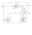
- FIG. 2 is a perspective view showing a schematic structure of the liquid crystal display device (display device) of the present embodiment.
- the liquid crystal display device of FIGS. 2 (a) and 2 (b) has a liquid crystal display panel 2 and a light guide.
- An element 4 is provided.
- two light guide elements 4 are arranged in the liquid crystal display panel 2 in the peripheral region along the two sides facing left and right of the peripheral region of the rectangular liquid crystal display panel 2.
- two liquid crystal display panels 2 are provided so that the end portions thereof are close to each other, and the light guide elements 4 mounted on the respective liquid crystal display panels 2 are connected to each other. Are in close contact with each other.
- liquid crystal display panels 2 are connected to each other by a movable mechanism (for example, a hinge or the like) not shown so that the relative angle of the display surface of the liquid crystal display panel 2 can be changed.
- a movable mechanism for example, a hinge or the like
- two liquid crystal display panels may be fixed so that their end portions are in contact with each other.
- the number of liquid crystal display panels is not limited to two, and three or more liquid crystal display panels may be connected to each other.
- the liquid crystal display panel 2 includes a display area in which a plurality of display elements (not shown) for displaying an image are arranged in a matrix, and a periphery of the display area where display cannot be performed because the display elements are not arranged Area (hereinafter referred to as a “frame area”).
- a display area in which a plurality of display elements (not shown) for displaying an image are arranged in a matrix, and a periphery of the display area where display cannot be performed because the display elements are not arranged Area (hereinafter referred to as a “frame area”).
- the light guide element 4 is, for example, a fiber (face) plate and has a function of guiding a part of light emitted from the display element by optical path conversion onto the frame area, in other words, a display of the liquid crystal display panel 2. It has a function of changing the area (display surface).
- the fiber plate is a shape in which single fibers having a diameter of several ⁇ m are bundled, and each single fiber is arranged so as to cover a core glass that transmits light and has a different refraction.
- a frame area where display cannot be performed is provided around the liquid crystal display panel.
- This frame region is provided because it is necessary as a clearance during manufacturing. That is, a plurality of substrates constituting the liquid crystal panel are manufactured after being formed on a single original substrate and then separated one by one. Therefore, the frame region is necessary as a clearance for the part to be cut off.
- this frame area is used as an area for applying a sealant for sealing liquid crystal, an area for providing signal wiring, spare wiring, inspection wiring, connection wiring, or a connection terminal for an external circuit.
- the liquid crystal display panel 2 having such a frame region cannot display an image in the frame region, and a plurality of liquid crystal display panels are arranged so that one side thereof is in contact with each other, thereby providing a large display screen. Even if configured, a single seamless display image cannot be obtained.
- the above guide is provided on the vicinity of the end (hereinafter referred to as the display area end) A 2 and on the frame area A 3 outside the display area.
- the optical element 4 By providing the optical element 4, the image of the display area end A2 is optically converted and displayed on the frame area A3. This makes it possible to obtain a seamless display image.
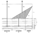
- the structure of the liquid crystal display panel 2 and the light guide element 4 will be described with reference to FIG.
- FIG. 3 is a partial cross-sectional view showing the structure of the liquid crystal display panel 2 and the light guide element 4.
- the paths (light paths) 6a and 6b of light emitted from the liquid crystal display panel 2 are illustrated by thick lines and arrows.
- the transparent cover 5 shown in FIG. 3 is provided to protect the liquid crystal display panel 2 and the light guide element 4 although not shown in FIG.
- FIG. 3 shows the liquid crystal display panel 2 and the light guide element in which the vicinity of the light guide element 4 is enlarged when the liquid crystal display panel shown in FIG. 2 is cut along the longitudinal direction (left and right direction in FIG. 2).
- Four cross sections are mainly shown.
- the light guide element 4 which is a fiber plate has a bottom surface on which light from the liquid crystal display panel 2 is incident (that is, a light incident surface of all single fibers constituting the fiber plate) on the display area end A2 of the liquid crystal display panel 2. It is glued to. Further, the light guide element 4 has an upper slope from which light from the liquid crystal display panel 2 is emitted (that is, the light emission surface of all single fibers) from directly above the display area end A2 to just above the frame area A3 of the liquid crystal display panel 2. It has a shape that covers (approaches) the range.
- the light emitted from the display area end A2 of the liquid crystal display panel 2 and incident on the light guide element 4 is changed in the optical path by the light guide element 4 and is emitted in the direction directly above the frame area A3. Then, an image is displayed as if there is no frame area A3 that cannot be displayed.
- the liquid crystal display panel 2 performs various displays by controlling the amount of light transmitted from a light source such as a light emitting diode (LED) included in the backlight device (LED: Light Emitting Diode), the upper surface of the liquid crystal display panel 2 A TFT (Thin Film Transistor) substrate 111 having a polarizing plate 110a attached thereto, a CF (Color Filter) substrate 113 having a polarizing plate 110b attached to the lower surface thereof, and a liquid crystal layer 112 sandwiched between these substrates.
- a light source such as a light emitting diode (LED) included in the backlight device (LED: Light Emitting Diode
- TFT Thin Film Transistor
- CF Color Filter
- the backlight device is provided such that the upper surface thereof is in contact with the lower surface of the liquid crystal display panel 2, and the light source (not shown) is provided at the end thereof, and the light guide plate emits light from the light source in a planar shape from the illumination surface.
- a lens sheet 115 made of a lens sheet or a light diffusion sheet disposed on the upper surface side (illumination surface side) of the light guide plate 116, and a lower surface side (opposite the illumination surface) of the light guide plate 116.
- a reflection sheet 117 attached thereto.
- the light from the light source of the backlight device is incident on a predetermined light incident surface of the light guide plate 116 and then diffused throughout the light guide plate 116, so that the surface from the illumination surface (light emitting surface) of the lens sheets 115 is planar. Is emitted.
- light emitted from the display area end A2 of the liquid crystal display panel 2 passes through the light guide element 4 and is a display area other than the display area end A2 of the liquid crystal display panel 2 (hereinafter, “ The light emitted from A1 (referred to as “normal display area”) is emitted outside the apparatus without passing through the light guide element 4 to form a display image.
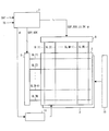
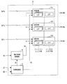
- FIG. 4 is a block diagram showing the overall configuration of the active matrix liquid crystal display device according to Embodiment 1 of the present invention.
- This liquid crystal display device includes a display control circuit 7, a video signal line drive circuit (source driver) 8, a scan signal line drive circuit (gate driver) 9, and a common electrode drive circuit 11, and a liquid crystal display panel 2. And a backlight unit composed of the backlight device 3 and the backlight drive circuit 10.
- the display control circuit 7 and the video signal line driving circuit 8 are often constituted by separate large-scale integrated circuit (Large Scale Integration Circuit: hereinafter abbreviated as “LSI”) chips. It is assumed to be composed of a chip (RAM built-in type source driver). Note that the drive control circuit obtained by adding the scanning signal line drive circuit 9 to this may be constituted by one LSI chip, or may be formed monolithically on the glass substrate of the liquid crystal panel instead of the chip.
- LSI Large Scale Integration Circuit
- the display section of the liquid crystal display panel 2 shown in FIG. 4 includes a plurality (M) of video signal lines SL (1) to SL (M) and a plurality (N) of scanning signal lines GL (1) to GL (N) and a plurality (M ⁇ N) of pixel forming portions (not shown, but not shown) provided corresponding to the intersections of the plurality of video signal lines and the plurality of scanning signal lines, respectively. Equivalent to).
- Each pixel forming unit is a switching element having a gate terminal connected to the scanning signal line GL (n) passing through the corresponding intersection and a source terminal connected to the video signal line SL (m) passing through the intersection.
- a TFT Thin Film Transistor: not shown
- a pixel electrode (not shown) connected to the drain terminal of the TFT
- a common electrode (“opposing”) provided in common to the plurality of pixel forming portions.
- a liquid crystal layer as an electro-optic element sandwiched between the pixel electrodes and the common electrode.
- each pixel forming unit actually sets one color pixel as a set of RGB pixels formed by each RGB (R: red, G: green, B: blue) pixel forming unit.
- the types of colors are not limited to the three types of RGB, and any number may be arbitrarily selected from six colors of RGBYCM (R: red, G: green, B: blue, Y: yellow, C: cyan, M: magenta). The type selected may be used.
- a line inversion driving method is employed which is a driving method for inverting the positive / negative polarity of the voltage applied to the liquid crystal layer of each pixel forming unit for each row in the display unit and for each frame. Is done.
- the display control circuit 7 receives an image signal DAT and a timing control signal TS sent from the outside, and receives a digital image signal DV, a source start pulse signal SSP and a source clock signal for controlling the timing for displaying an image on the display unit.
- SCK, latch strobe signal LS, gate start pulse signal GSP, gate clock signal GCK, and polarity inversion signal ⁇ are output.
- the display control circuit 7 performs appropriate correction (gamma correction or the like) so as to compensate for a difference in display characteristics (such as gamma characteristics) between the normal display area A1 and the display area end A2 with respect to the received image signal DAT. ) And output as a digital image signal DV (corrected image signal). Details of this operation and configuration will be described later.
- the video signal line driving circuit 8 receives the digital image signal DV, the source start pulse signal SSP, the source clock signal SCK, and the latch strobe signal LS output from the display control circuit 7 and receives the pixel capacitance of each pixel forming unit in the display unit. To charge the video signal lines SL (1) to SL (M). At this time, the video signal line driving circuit 8 sequentially holds the digital image signal DV indicating the voltage to be applied to each of the video signal lines SL (1) to SL (M) at the timing when the pulse of the source clock signal SCK is generated. Is done.
- the held digital image signal DV is converted into an analog voltage at the timing when the pulse of the latch strobe signal LS is generated.
- the converted analog voltage is applied simultaneously to all the video signal lines SL (1) to SL (M) as drive video signals. That is, in the present embodiment, the line sequential driving method is adopted as the driving method of the video signal lines SL (1) to SL (M). Note that the polarity of the video signal applied to each of the video signal lines SL (1) to SL (M) is inverted in accordance with the polarity inversion signal ⁇ for AC driving of the display unit.
- the scanning signal line drive circuit 9 Based on the gate start pulse signal GSP and the gate clock signal GCK output from the display control circuit 7, the scanning signal line drive circuit 9 sends active scanning signals to the scanning signal lines GL (1) to GL (N). Apply sequentially.
- the common electrode drive circuit 11 generates a common voltage Vcom that is a voltage to be applied to the common electrode of the liquid crystal.
- Vcom a common voltage to be applied to the common electrode of the liquid crystal.
- the potential of the common electrode is also changed according to the AC drive.
- the common electrode driving circuit may be provided in the display control circuit 7 or the scanning signal line driving circuit 9.
- the driving video signal is applied to the video signal lines SL (1) to SL (M), and the scanning signal is applied to the scanning signal lines GL (1) to GL (N).
- the light transmittance of the liquid crystal layer is controlled, and an image is displayed on the display unit of the liquid crystal display panel 2.
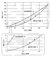
- FIG. 5 shows the liquid crystal display device in which the luminance per unit area of the liquid crystal display device in the normal display region A1 (hereinafter referred to as surface luminance) and the optical path length of a single fiber among the display region end A2 are maximized. It is the graph which compared surface luminance.
- the transmittance of the liquid crystal display panel is 7%
- the transmittance at which the optical path length of the single fiber of the light guide element is maximum is 30%
- the surface brightness of the light emitting surface of the backlight is the normal display area A1 and display area. It is set to 5200 cd / m 2 which is equal to the end A2, and the surface luminance of the liquid crystal display device in the normal display area A1 is set to 360 cd / m 2 at the maximum gradation.
- the surface luminance of the liquid crystal display device at the point where the optical path length of the single fiber is maximum in the display region end A2 is attenuated to about 30% with respect to the surface luminance of the liquid crystal display device in the normal display region A1.
- the luminance is reduced in the region where the light guide element is provided, and the degree of the luminance reduction of R, G, and B varies, a color shift or the like also occurs, thereby providing the light guide element.
- the boundary between the area that is provided and the area that is not provided is clearly recognized by the observer, and the observer feels uncomfortable. That is, in the liquid crystal display device of FIG. 2A, the frame area is clearly recognized, and in the liquid crystal display device of FIG. 2B, the boundary between the displays is clearly recognized. The viewer feels uncomfortable with what appears to be a single display.
- the transmittance of the liquid crystal display panel is manipulated and corrected, for example, the luminance at each gradation so that the gamma characteristic of the normal display area A1 matches the gamma characteristic of the display area end A2. It is also conceivable to correct the image signal given to the display element in the normal display area A1 so as to reduce the image quality. That is, if it is easy to understand, the maximum brightness of the display area end A2 that must be lower than the maximum brightness of the normal display area A1 cannot be increased anymore. It is impossible to match the gamma characteristics of A2. Therefore, since the surface brightness of the normal display area A1 is matched with the surface brightness of the liquid crystal display device at the lowered display area end A2, the display characteristics of the original liquid crystal display device are greatly impaired. .
- the luminance per unit area on the light emitting surface of the backlight device 3, that is, the illumination surface of the lens sheets 115 is higher than that of the normal display area A 1 where the light guide element 4 is not provided.
- the display area end A2 provided is made larger.
- the case where the number of light sources arranged for each of the normal display area A1 and the display area end A2 is adjusted will be described below.
- the backlight device 3 is provided with a plurality of LEDs 203 as light sources, and the unit area of the LEDs 203 arranged corresponding to the display region end A2 on the arrangement surface B of the LEDs 203.
- the number per unit is made larger than the number per unit area of the LEDs 203 arranged corresponding to the normal display area A1.
- the surface luminance of the light emitting surface of the backlight device 3 at the display region end A2 can be made larger than the surface luminance of the light emitting surface of the backlight device 3 at the normal display region A1, and the display region end A2 Therefore, it is possible to suppress a decrease in luminance of the liquid crystal display device. As a result, there is an effect that the difference in luminance emitted from the display device between the region where the light guide element is provided and the region where the light guide element is not provided is reduced, and the viewer does not feel uncomfortable.
- the backlight can be either an edge light type or a direct type, and the light source is not limited to the LED.
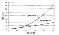
- FIG. 9 shows the normal display area A1 when the surface luminance of the light emitting surface of the backlight in the normal display area A1 is 5200 cd / m 2 and the surface luminance of the light emitting surface of the backlight at the display area end A2 is 17300 cd / m 2.
- 4 shows input gradation-output luminance characteristics (gamma characteristics) before image signal correction at the display area end A2 and gamma characteristics after image signal correction in both areas.
- the output luminance of the display area end A2 is the input gradation level. It can be seen that the output luminance of the normal display area A1 exceeds the entire range.
- the surface brightness of the light emitting surface of the backlight at the display area end A2 is preferably adjusted so that the brightness at the maximum gradation (maximum gradation brightness) in both areas is equal. This is because the luminance difference between the two regions can be reduced by equalizing the maximum gradation luminance in both regions.
- the adjustment of the surface brightness is not limited to the above method. Details will be described below.
- the maximum gradation luminance is the maximum luminance per unit area of the liquid crystal display device when displaying the maximum gradation in each of the normal display area A1 and the display area end A2.
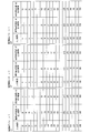
- FIG. 10 shows a look-up table (hereinafter referred to as LUT) 2 for performing gamma correction on the normal display area A1 and LUT1 for performing gamma correction on the display area end A2 corresponding to the gamma correction curve shown in FIG. Is shown.
- LUT look-up table
- the output gradation for the input gradation 255 is 255 for the normal display area A1 and 250 for the display area end A2 for any color.
- the output gradation for the input gradation 11 is 37 for the normal display area A1 and 5 for the display area end A2 for any color.
- gamma correction it is preferable to perform gamma correction independently for each RGB color in order to perform correction with higher accuracy. At this time, only the image signal of a color with a large color shift may be gamma-corrected, and it is most preferable to improve the accuracy by performing gamma correction according to the gamma characteristic of each color for all the RGB colors.
- FIG. 6 is a block diagram showing a configuration of the display control circuit 7 in the present embodiment.
- the display control circuit 7 is arranged at the display area end A2 among the timing control unit 13 that performs timing control regarding signal transmission and reception between the respective parts constituting the liquid crystal display device and the display elements arranged in a matrix.
- a correction area address storage unit 14 that stores a correction area address AD, which will be described later, and a pixel value (display gradation data) included in the image signal DAT, and a display that gives the pixel value
- a correction area address storage unit 14 that stores a correction area address AD, which will be described later, and a pixel value (display gradation data) included in the image signal DAT, and a display that gives the pixel value
- the timing control unit 13 shown in FIG. 6 receives a timing control signal TS sent from the outside, and displays an image on the control signal CT for controlling the operation of the data correction unit 12 and the display unit of the liquid crystal display panel 2.
- a source start pulse signal SSP, a source clock signal SCK, a latch strobe signal LS, a gate start pulse signal GSP, a gate clock signal GCK, and a polarity inversion signal ⁇ for controlling timing are output.
- the correction area address storage unit 14 is an example of information for specifying the position of a display element that corrects an image signal among display elements arranged in a matrix.
- the information for specifying the position of the display element to be corrected is not limited to the address on the RAM. In short, it is only necessary to be able to specify the positions of the display elements arranged in a matrix, so that the positions of the display elements can be specified by (x, y) coordinates by applying a two-dimensional coordinate system to the matrix arrangement. .
- the data correction unit 12 receives a pixel value (display gradation data) included in the image signal DAT, and (temporarily) stores it in a RAM described later, and stores the address of a memory cell in the RAM storing the pixel value. To do. Thereafter, the data correction unit 12 sequentially reads out the pixel values stored in the RAM based on the control signal CT from the timing control unit 13, and the address of the read pixel value is stored in the correction area address storage unit 14. If it matches any of the correction area addresses AD, the pixel value is corrected. Alternatively, at least one of the pixel values is corrected depending on whether the address of the read pixel value matches the correction area address AD or not.
- the data correction unit 12 brings the gamma characteristic of the display area end A2 where the light guide element 4 is provided and the gamma characteristic of the normal display area A1 where the light guide element 4 is not provided close to each other.
- gamma correction is performed to correct at least one of the image signal to be applied to the display element at the display area end A2 and the image signal to be applied to the display element at the normal display area A1, and thereby obtained.
- the result is output as a digital image signal DV.
- FIG. 7 is a block diagram showing a configuration of the data correction unit 12 included in the display control circuit 7 in the present embodiment.
- the data correction unit 12 includes a blue RAM 101 that stores an LUT for correcting display data DATb for a blue pixel located at the display area end A2, and a display data for a green pixel located at the display area end A2.
- Each color RAM is composed of three semiconductor chips, but may be three different storage areas in one semiconductor chip, or may be a part of a semiconductor memory or the like constituting the correction area address storage unit 14. Good.
- the RAM control unit 15 outputs a RAM control signal CS based on the control signal CT sent from the timing control unit 13.
- the RAM control signal CS includes, for example, the addresses of the memory cells for sequentially storing the pixel values included in the display data DATb of the blue pixels in the memory cells in the blue RAM 101, and the LUT stored in each color RAM. , And a read address for designating an appropriate LUT.
- the correction area control unit 16 receives the RAM control signal CS from the RAM control unit 15 and acquires the address of the memory cell corresponding to the pixel value currently written in the RAM for each color from the RAM control signal CS. Further, the correction area control unit 16 compares the acquired memory cell address with the correction area address AD read from the correction area address storage unit 14, and if they match, the memory of the matching address is found. A pixel value is read from the cell, and a correction instruction signal SS for instructing the LUT designated by the RAM control unit 15 to input the read pixel value is given to each color RAM.
- FIG. 8 simply shows two examples of the internal configuration of each color RAM.
- FIG. 8A shows a case where each color RAM has only an LUT corresponding to the display area end A2, and
- FIG. 8B shows each of the normal display area A1 and the display area end A2. The case where both the LUTs corresponding to is provided is shown.
- FIG. 8B when the correction instruction signal SS is input to the B RAM 101, the route on the upper side in the figure is advanced so that the LUT 1 specified by the RAM control signal CS is used, and the display area end portion is displayed. A pixel value corresponding to A2 is read from the storage area in the B RAM 101, corrected by the LUT1, and output as a corrected image signal DV.
- a reference display characteristic is determined, and the display characteristics of the normal display area A1 and the display area end A2 are corrected to match the reference display characteristic. Further, in this case, the respective image signals DAT corresponding to both the normal display area A1 and the display area end A2 can be corrected, the difference in display characteristics between the two areas can be further reduced, and the optimum display characteristics can be obtained. There is an effect that can be obtained.
- the method of correcting the image signal is as follows. The following two types are conceivable.
- the gamma characteristic of the area where the light guide element is provided is matched with the gamma characteristic of the area where the light guide element is not provided.
- FIG. 9 shows a case where the gamma characteristic is corrected by the method (2)
- FIG. 10 shows LUT2 corresponding to the normal display area A1 and LUT1 corresponding to the display area end A2.
- the reference gamma characteristic is an intermediate characteristic between the gamma characteristic of the display area end A2 and the gamma characteristic of the normal display area A1.
- the normal display area A1 is subjected to gamma correction that increases the output brightness, whereas the display area end A2 is subjected to gamma correction that decreases the output brightness.
- the surface brightness at the maximum gradation of the liquid crystal display device in the display area end A2 is set so as not to exceed the surface brightness at the maximum gradation of the liquid crystal display device in the normal display area A1
- the correction method can be considered.
- the gamma characteristic of the area where the light guide element is not provided is matched with the gamma characteristic of the area where the light guide element is provided.
- the surface brightness at the maximum gradation of the liquid crystal display device in the display area end A2 is set to coincide with the surface brightness at the maximum gradation of the liquid crystal display device in the normal display area A1
- the backlight luminance at the display area end A2 is increased, so that the black image display at the display area end A2 is displayed in the normal display area A1 as shown in FIG. Compared with the black image display, the observer feels uncomfortable.
- FIG. 11 shows that a surface brightness of about 4 cd / m 2 is observed when a black image is displayed at the display area end A2 (input 0 gradation), and a slightly grayish black is displayed. Show.
- black floating is a phenomenon in which black that should originally be displayed is displayed as grayish black with respect to input 0 gradation.
- the backlight luminance is controlled by a plurality of patterns according to the average gradation of the image signal DAT, and the image signal applied to the display element at the display area end A2 is the plurality of patterns.
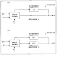
- FIG. 12 is a block diagram showing an overall configuration of an active matrix liquid crystal display device according to Embodiment 2 of the present invention.
- the backlight driving circuit 10 is configured to drive the backlight according to the average gradation of the image signal DAT.
- the backlight drive circuit 10 receives the backlight control signal BL for controlling the backlight drive current from the display control circuit 7, and applies the drive current applied to the backlight device 3 in accordance with the backlight control signal BL. Is controlling.
- FIG. 13 is a block diagram showing the overall configuration of the display control circuit 7 in Embodiment 2 of the present invention.
- an input tone determination unit 17 an average tone detection unit and a backlight control unit
- the input gradation determination unit 17 calculates the average gradation of the image signal of the display area end A2 in the image signal DAT, and according to the calculated average gradation, the input gradation determination unit 17
- the backlight control signal BL for controlling the backlight driving current and the control signal BS for selecting the correction gradation pattern are output.
- the output control signal BS is input to the data correction unit 12.
- FIG. 14 is a block diagram showing a configuration of the data correction unit 12 included in the display control circuit 7 according to the second embodiment of the present invention.
- the basic configuration is the same as in the first embodiment, but differs in that each color RAM has a plurality of LUTs for the display area end A2 (fiber area) in accordance with the number of gradation correction patterns.
- the control signal BS Input to the RAM controller 15.
- the RAM control unit 15 outputs the RAM control signal CS for selecting the LUT suitable for the correction gradation pattern designated by the control signal BS to each corresponding color RAM.
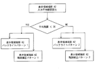
- FIG. 15 shows a flowchart for dividing the backlight drive current and the gradation correction of the image signal into three types of patterns according to the average gradation of the image signal at the display area end A2.
- the gradation is divided into three patterns of average gradation 134 or higher, average gradation 27 or higher and lower than 133, and average gray scale 27, and the correction pattern of the display area end A2 is backed up when the average gradation is 134 or higher.
- Write pattern 1 and gradation correction pattern 1 backlight pattern 2 and gradation correction pattern 2 when the average gradation is 27 or more and less than 133, and backlight pattern 3 and gradation correction pattern when the average gradation is less than 27 Three.
- the number of patterns to be divided and the gradation to be divided can be obtained as described below using, for example, the following Equation 1.
- FIG. 16A shows the surface luminance of the maximum gradation of the liquid crystal display device in the display area end A2 as shown in FIG. 9 of the first embodiment, and the maximum gradation of the liquid crystal display device in the normal display area A1.
- 16 is a graph showing how the average gradation selection values (134 and 27) shown in the flowchart of FIG.
- FIG. 16A shows the gamma characteristic (curve a) of the liquid crystal display device in the normal display area A1 before the image signal correction, and the average gradation size in the display area end A2.
- 4 shows gamma characteristics (curves b, c, d) of the liquid crystal display device when the amount of light of the backlight is adjusted according to the backlight patterns 1 to 3 adapted to the above.
- 16B to 16D show the backlight patterns 1 to 3 as gradation-luminance curves, respectively.
- the backlight pattern 1 is applied as it is and the backlight is driven. Does not reduce the current.
- the surface luminance of the liquid crystal display device at the time of maximum gradation display is maintained at about 360 cd / m 2 .
- the backlight pattern 2 is applied and the backlight driving current is set. It is lowered. That is, as the average gradation at the display area end A2 becomes lower, the gradient of the gamma characteristic at the display area end A2 increases, and the gradation corresponding to the normal display area A1 cannot be expressed sufficiently (different gradations). However, at the time of low gradation, the backlight driving current at the display area end A2 can be lowered, and the gradation corresponding to the normal display area A1 can be expressed sufficiently.
- the image signal is corrected by the gradation correction pattern at the display area end A2.
- the gradation correction pattern will be described later.
- the gamma characteristic corresponding to the backlight pattern 2 shown by the curve c in FIG. 16A can sufficiently express the gradation corresponding to the normal display area A1 with less than 134 gradations (the same for different gradations).
- the luminance of the backlight does not exist, and the backlight driving current is reduced.
- the light amount of the backlight is adjusted so that the surface luminance of the liquid crystal display device at the time of maximum gradation display is about 100 cd / m 2 . .
- the gradation range satisfying the condition of the above expression 1 is examined by comparing the gamma characteristics of the above (the curve a in FIG. 16A)
- the above expression 1 is not satisfied in the gradation range of the gradation 27 or higher. It can be seen that the above expression 1 is satisfied when the gradation range is less than 27.
- the backlight pattern 2 is applied in the region not satisfying the above formula 1 to reduce the backlight drive current
- the backlight pattern 3 is applied in the region satisfying the above formula 1 to further reduce the backlight drive current.
- the method of reducing the drive current of the backlight is the same as described above.
- the amount of light of the backlight is adjusted so that the surface brightness of the liquid crystal display device at the time of maximum gradation display is about 6 cd / m 2. Yes.
- the normal display area is corrected by further correcting the image signal.
- the gradation corresponding to A1 can be sufficiently expressed, and the average gradation at the display area end A2 is 27 gradations or more and 133 gradations or less, and the average gradation at the display area end A2 is 26 gradations.
- the gradation corresponding to the normal display area A1 can be sufficiently expressed.
- average gradation was calculated
- the above control can be applied when light sources such as LEDs are arranged in a matrix in accordance with the display area of the liquid crystal display panel 2 and a surface light source is configured in combination with a diffusion plate or the like. That is, the display area end A2 is divided into a plurality of small areas, an average gradation is obtained for each small area, and the light quantity and image signal of the LED corresponding to the small area are based on the flowchart of FIG. May be controlled.
- FIG. 17 shows LUTs in the gradation correction patterns 1 to 3 shown in the flowchart of FIG. Each gradation correction pattern is interlocked with the backlight patterns 1 to 3 in FIGS. 16B to 16D.
- the gradation correction pattern 1 has 134 gradations or more
- the gradation correction pattern 2 has the 27th floor.
- the gradation correction pattern 3 is 26 gradations or less
- the gamma characteristic of the display area end A2 approximates the gamma characteristic of the normal display area A1, and corresponds to the normal display area A1.
- the gradation is adjusted so that the gradation to be expressed can be sufficiently expressed (the gradation with the same luminance does not exist even with different gradations). As a result, the display image can be viewed without a sense of incongruity as if there is no boundary between the two regions for the observer.
- the normal gradation in the normal display area A1 and the display area end A2 Is set equal to the maximum luminance (for example, 360 cd / m 2 ), the display image in the entire gradation range is brighter than the display image of the same gradation in the normal display region A1 at the display area end A2. I can see it. Therefore, according to the gradation correction pattern 1, the image signal is corrected so that the output gradation relative to the input gradation is lower than the normal display area A1 at the display area end A2 in all gradation ranges.
- the backlight is controlled by the backlight pattern 2, and the backlight driving current is set so that the surface brightness of the liquid crystal display device at the time of maximum gradation display is about 100 cd / m 2. Therefore, according to the gradation correction pattern 2, the image signal is corrected so that the gradation corresponding to the normal display area A1 can be sufficiently expressed in the range of the low gradation and the middle gradation. As a result, it is possible to express the low gradation and medium gradation colors of the normal display area A1 that cannot be sufficiently reproduced by the backlight pattern 1.
- the backlight is controlled by the backlight pattern 3, and the backlight driving current is set so that the surface luminance of the liquid crystal display device at the time of maximum gradation display is about 6 cd / m 2. Therefore, according to the gradation correction pattern 3, the image signal is corrected so that the gradation corresponding to the normal display area A1 can be sufficiently expressed, particularly in the low gradation range. As a result, it is possible to express the low gradation color of the normal display area A1 that cannot be sufficiently reproduced by the backlight pattern 2. Further, since the luminance of 1 cd / m 2 or less which cannot be sufficiently expressed by the backlight pattern 2 can be expressed, the contrast is also improved.
- the present invention is not limited to this, and as shown in the flowchart of FIG. .
- the effect of losing a sense of incongruity may be less than in the case of dividing into three patterns, the design can be simplified and the cost can be reduced by reducing the memory.
- a display device has a region in which the light guide element has a maximum luminance per unit area in which the light guide element is not provided.
- the display device is characterized by being approximately equal to the maximum luminance per unit area of the display device.
- the brightness of the backlight is adjusted so that the maximum brightness of each of the area where the light guide element is provided and the area where the light guide element is not provided are substantially equal. Therefore, there is an effect that the luminance difference emitted from the display device between the two areas is reduced and the viewer does not feel uncomfortable.
- the display device includes a plurality of light sources, and relates to the number of light sources per unit area on the arrangement surface of the light sources.
- the number of light sources arranged corresponding to the provided area is larger than the number of light sources arranged corresponding to the area where the light guide element is not provided.
- the number of light sources per unit area on the light source arrangement surface is relatively increased, thereby reducing the luminance caused by the light guide element. Can be compensated.
- the display device includes a plurality of light sources, and one light source disposed corresponding to a region where the light guide element is provided.
- the maximum light emission luminance per area is larger than the maximum light emission luminance per light source arranged corresponding to the region where the light guide element is not provided.
- a light source having a maximum light emission luminance in other words, a light emitting ability that is relatively large, is arranged to compensate for a decrease in luminance caused by the light guide element. can do.
- the display device makes the gamma characteristic of the region where the light guide element is provided and the gamma characteristic of the region where the light guide element is not provided close to each other. Further, among the image signals, a gamma for correcting at least one of an image signal given to a display element in a region where the light guide element is provided and an image signal given to a display element in a region where the light guide element is not provided An image signal correction unit that outputs a result obtained by the correction as a corrected image signal is provided.
- the display method brings the gamma characteristics of the area where the light guide element is provided and the gamma characteristics of the area where the light guide element is not provided closer to each other.
- the image signals at least an image signal to be given to a display element in a region where the light guide element is provided and an image signal to be given to a display element in a region where the light guide element is not provided
- An image signal correction step for outputting a result obtained by gamma correction for correcting one as a corrected image signal, and a region of the light guide element in accordance with the corrected image signal obtained in the image signal correction step.
- a driving step for driving the display element.
- the display device includes a plurality of types of display elements that emit different colors, and the image signal correction unit includes at least one of the different colors.
- the gamma correction is performed for one color.
- the gamma characteristic of the region where the light guide element is provided and the gamma characteristic of the region where the light guide element is not provided are further approximated, so that the viewer is not further discomforted. Play.
- the display device includes a plurality of types of display elements that emit different colors, and the image signal correction unit performs the above-described processing for all the different colors. It is characterized by performing gamma correction.
- the gamma characteristic of the region where the light guide element is provided and the gamma characteristic of the region where the light guide element is not provided are further approximated, so that the viewer is not further discomforted. Play.
- the image signal correction unit uniformly performs the gamma correction regardless of colors.
- the same gamma correction is performed for all the different colors. That is, when the input gradation of any color is set to the same value so that an achromatic color is displayed for all gradations from white display to black display on the display device, the output gradation becomes the same value regardless of the color. As a result, the difference in luminance generated between the region where the light guide element is provided and the region where the light guide element is not provided can be reduced by a simple method, and the viewer can be prevented from feeling more uncomfortable. .
- the display device receives the image signal and detects an average gradation of the image signal input to an area where the light guide element is provided. And a backlight control unit that controls a drive current for driving the backlight, and the backlight control unit reduces the drive current when the average gradation value is lower than a reference value. It is characterized by making it.
- the low gradation image is excellent in a state close to the original gradation. Since it is displayed, it is possible to provide a display device capable of realizing high contrast.
- the display device uses the reference value as the reference value so as to divide the entire gradation range from the lowest gradation to the highest gradation into at least three gradation ranges.
- the backlight control unit reduces the drive current by a pattern according to a gradation range in which at least two reference values are set and the average gradation value is included.
- the gradation range in which the average gradation value is lower than the reference value is at least 2 on the low gradation side.
- the lower reference value of the two reference values is lower, the lower gradation range, and the lower reference value.
- the degree of luminance change with respect to gradation change differs from the gradation range on the high gradation side.
- the method of reducing the drive current in accordance with the degree of the luminance change with respect to the gradation change it is preferable to change the method of reducing the drive current in accordance with the degree of the luminance change with respect to the gradation change. That is, as the number of sections in the entire gradation range is increased and the control pattern of the backlight driving current is increased accordingly, the area between the area where the light guide element is provided and the area where the light guide element is not provided is increased. The effect of reducing the difference in brightness and color to be generated and preventing the viewer from feeling more uncomfortable.
- the display device receives the image signal and detects an average gradation of the image signal input to an area where the light guide element is provided. And a backlight control unit that controls a drive current for driving the backlight, and the backlight control unit reduces the drive current when the average gradation value is lower than a reference value.
- the image signal correction unit is characterized in that the backlight control unit changes a gamma correction pattern according to a pattern for reducing the drive current.
- the display device is characterized in that the display panel is a liquid crystal display panel.
- the display device includes a plurality of the display panels so as to be close to or in contact with at least one other display panel, the light guide element, and the other
- the other light guide elements provided in the display panel are arranged so as to be in contact with each other without any gap.
- a combination of a configuration described in a certain claim and a configuration described in another claim is limited to a combination of the configuration described in the claim cited in the claim.
- combinations with configurations described in the claims not cited in the focused claims are possible.
- the present invention can be applied to various direct-view display devices.
Priority Applications (6)
| Application Number | Priority Date | Filing Date | Title |
|---|---|---|---|
| US13/138,246 US8659504B2 (en) | 2009-05-29 | 2010-05-14 | Display device and display method |
| RU2011132281/28A RU2565480C2 (ru) | 2009-05-29 | 2010-05-14 | Дисплейное устройство и способ отображения |
| BRPI1008917A BRPI1008917A2 (pt) | 2009-05-29 | 2010-05-14 | dispositivo de exibição e método de exibição |
| CN201080005937.8A CN102301273B (zh) | 2009-05-29 | 2010-05-14 | 显示装置和显示方法 |
| JP2011515976A JP5186597B2 (ja) | 2009-05-29 | 2010-05-14 | 表示装置および表示方法 |
| EP10780428.8A EP2437103A4 (en) | 2009-05-29 | 2010-05-14 | DISPLAY APPARATUS AND DISPLAY METHOD |
Applications Claiming Priority (2)
| Application Number | Priority Date | Filing Date | Title |
|---|---|---|---|
| JP2009131553 | 2009-05-29 | ||
| JP2009-131553 | 2009-05-29 |
Publications (1)
| Publication Number | Publication Date |
|---|---|
| WO2010137473A1 true WO2010137473A1 (ja) | 2010-12-02 |
Family
ID=43222585
Family Applications (1)
| Application Number | Title | Priority Date | Filing Date |
|---|---|---|---|
| PCT/JP2010/058222 WO2010137473A1 (ja) | 2009-05-29 | 2010-05-14 | 表示装置および表示方法 |
Country Status (7)
| Country | Link |
|---|---|
| US (1) | US8659504B2 (zh) |
| EP (1) | EP2437103A4 (zh) |
| JP (1) | JP5186597B2 (zh) |
| CN (1) | CN102301273B (zh) |
| BR (1) | BRPI1008917A2 (zh) |
| RU (1) | RU2565480C2 (zh) |
| WO (1) | WO2010137473A1 (zh) |
Cited By (1)
| Publication number | Priority date | Publication date | Assignee | Title |
|---|---|---|---|---|
| JP2016133525A (ja) * | 2015-01-15 | 2016-07-25 | 株式会社東芝 | 輝度補正装置、画像表示装置および輝度補正方法 |
Families Citing this family (24)
| Publication number | Priority date | Publication date | Assignee | Title |
|---|---|---|---|---|
| US20130083080A1 (en) | 2011-09-30 | 2013-04-04 | Apple Inc. | Optical system and method to mimic zero-border display |
| KR101965207B1 (ko) * | 2012-03-27 | 2019-04-05 | 삼성디스플레이 주식회사 | 표시 장치 |
| KR20140000458A (ko) * | 2012-06-22 | 2014-01-03 | 삼성디스플레이 주식회사 | 표시 장치 및 그 구동 방법 |
| WO2014070647A2 (en) * | 2012-11-02 | 2014-05-08 | Corning Incorporated | Immersive display with minimized image artifacts |
| CN103969864B (zh) * | 2013-02-05 | 2017-09-26 | 鸿富锦精密工业(深圳)有限公司 | 显示元件、显示装置及拼接式显示器 |
| JP5771241B2 (ja) * | 2013-06-28 | 2015-08-26 | 双葉電子工業株式会社 | 表示駆動装置、表示駆動方法、表示装置 |
| KR102148823B1 (ko) | 2013-08-21 | 2020-08-28 | 삼성디스플레이 주식회사 | 멀티 패널 표시 장치 |
| CN104517534A (zh) * | 2013-09-27 | 2015-04-15 | 业鑫科技顾问股份有限公司 | 图像补偿元件、显示装置及拼接式显示器 |
| TWI492202B (zh) * | 2013-09-27 | 2015-07-11 | Ye Xin Technology Consulting Co Ltd | 顯示裝置及拼接式顯示器 |
| TWI507943B (zh) * | 2013-09-27 | 2015-11-11 | Ye Xin Technology Consulting Co Ltd | 觸控顯示裝置及拼接式觸控顯示器 |
| KR20150093893A (ko) | 2014-02-07 | 2015-08-19 | 삼성디스플레이 주식회사 | 표시 장치 |
| KR20150102803A (ko) * | 2014-02-28 | 2015-09-08 | 삼성디스플레이 주식회사 | 표시 장치 |
| CN105869598B (zh) * | 2016-06-07 | 2019-06-11 | 武汉华星光电技术有限公司 | 液晶显示器的驱动方法以及液晶显示器 |
| KR102637181B1 (ko) * | 2016-11-18 | 2024-02-15 | 삼성디스플레이 주식회사 | 표시 장치 및 그 구동 방법 |
| GB2558000B (en) * | 2016-12-21 | 2020-06-10 | Apical Ltd | Display control |
| CN107221307A (zh) * | 2017-07-31 | 2017-09-29 | 京东方科技集团股份有限公司 | 显示模组的补偿方法和补偿装置 |
| JP2019070770A (ja) * | 2017-10-11 | 2019-05-09 | シャープ株式会社 | 液晶表示装置および電子装置 |
| CN107564470B (zh) * | 2017-10-31 | 2019-09-24 | 京东方科技集团股份有限公司 | 一种有机发光显示面板的亮度调节方法及相关装置 |
| CN108318960B (zh) * | 2018-02-11 | 2020-11-06 | 惠州市华星光电技术有限公司 | 导光模块及无缝拼接屏 |
| US20200225903A1 (en) * | 2019-01-10 | 2020-07-16 | Noy Cohen | Modular display system |
| CN111696446B (zh) * | 2019-03-14 | 2023-08-04 | 诚屏科技股份有限公司 | 多荧幕显示装置 |
| US11284193B2 (en) * | 2020-02-10 | 2022-03-22 | Laurie Cline | Audio enhancement system for artistic works |
| US11067745B1 (en) * | 2020-07-20 | 2021-07-20 | Seamless Technology Inc. | Display assembly including at least two display devices |
| CN113885255B (zh) * | 2021-11-01 | 2023-12-29 | 厦门天马微电子有限公司 | 背光模组和显示装置 |
Citations (4)
| Publication number | Priority date | Publication date | Assignee | Title |
|---|---|---|---|---|
| JPS60202422A (ja) * | 1984-03-27 | 1985-10-12 | Seiko Epson Corp | 大型表示装置 |
| JPH07128652A (ja) | 1993-10-28 | 1995-05-19 | Hewlett Packard Co <Hp> | 液晶表示装置 |
| JP2000056713A (ja) | 1998-08-04 | 2000-02-25 | Sharp Corp | ディスプレイユニットおよび複合型ディスプレイ、並びに、ディスプレイモジュール |
| JP2001005414A (ja) | 1999-05-31 | 2001-01-12 | Samsung Sdi Co Ltd | マルチディスプレイ装置 |
Family Cites Families (10)
| Publication number | Priority date | Publication date | Assignee | Title |
|---|---|---|---|---|
| EP0835504A4 (en) * | 1996-03-25 | 2000-07-26 | Rainbow Displays Inc | GRID OF FLAT SCREENS HAVING A COLOR CORRECTION FUNCTION |
| US6115092A (en) * | 1999-09-15 | 2000-09-05 | Rainbow Displays, Inc. | Compensation for edge effects and cell gap variation in tiled flat-panel, liquid crystal displays |
| CN101206327B (zh) * | 2006-12-20 | 2011-11-30 | 欧睿控股股份有限公司 | 无接缝显示器及制造无接缝显示器的方法 |
| KR101323389B1 (ko) * | 2006-12-29 | 2013-10-29 | 엘지디스플레이 주식회사 | 백라이트 유닛과 이를 갖는 표시 장치 |
| JP2009002976A (ja) * | 2007-06-19 | 2009-01-08 | Renesas Technology Corp | 表示駆動回路 |
| US8031166B2 (en) * | 2007-11-06 | 2011-10-04 | Hisense Beijing Electric Co., Ltd. | Liquid crystal display method and the appratus thereof |
| CN101868814B (zh) * | 2007-11-22 | 2013-06-05 | 夏普株式会社 | 显示装置 |
| WO2009122691A1 (ja) | 2008-03-31 | 2009-10-08 | シャープ株式会社 | 表示装置 |
| JP5490710B2 (ja) | 2008-10-24 | 2014-05-14 | シャープ株式会社 | 表示装置および表示装置の駆動方法 |
| US8279351B2 (en) * | 2008-10-27 | 2012-10-02 | Rgb Systems, Inc. | Method and apparatus for hardware-efficient continuous gamma curve adjustment |
-
2010
- 2010-05-14 US US13/138,246 patent/US8659504B2/en not_active Expired - Fee Related
- 2010-05-14 RU RU2011132281/28A patent/RU2565480C2/ru not_active IP Right Cessation
- 2010-05-14 BR BRPI1008917A patent/BRPI1008917A2/pt not_active IP Right Cessation
- 2010-05-14 WO PCT/JP2010/058222 patent/WO2010137473A1/ja active Application Filing
- 2010-05-14 CN CN201080005937.8A patent/CN102301273B/zh not_active Expired - Fee Related
- 2010-05-14 JP JP2011515976A patent/JP5186597B2/ja not_active Expired - Fee Related
- 2010-05-14 EP EP10780428.8A patent/EP2437103A4/en not_active Withdrawn
Patent Citations (4)
| Publication number | Priority date | Publication date | Assignee | Title |
|---|---|---|---|---|
| JPS60202422A (ja) * | 1984-03-27 | 1985-10-12 | Seiko Epson Corp | 大型表示装置 |
| JPH07128652A (ja) | 1993-10-28 | 1995-05-19 | Hewlett Packard Co <Hp> | 液晶表示装置 |
| JP2000056713A (ja) | 1998-08-04 | 2000-02-25 | Sharp Corp | ディスプレイユニットおよび複合型ディスプレイ、並びに、ディスプレイモジュール |
| JP2001005414A (ja) | 1999-05-31 | 2001-01-12 | Samsung Sdi Co Ltd | マルチディスプレイ装置 |
Non-Patent Citations (1)
| Title |
|---|
| See also references of EP2437103A4 |
Cited By (1)
| Publication number | Priority date | Publication date | Assignee | Title |
|---|---|---|---|---|
| JP2016133525A (ja) * | 2015-01-15 | 2016-07-25 | 株式会社東芝 | 輝度補正装置、画像表示装置および輝度補正方法 |
Also Published As
| Publication number | Publication date |
|---|---|
| JPWO2010137473A1 (ja) | 2012-11-12 |
| RU2565480C2 (ru) | 2015-10-20 |
| EP2437103A1 (en) | 2012-04-04 |
| CN102301273A (zh) | 2011-12-28 |
| RU2011132281A (ru) | 2013-07-10 |
| US20110279487A1 (en) | 2011-11-17 |
| US8659504B2 (en) | 2014-02-25 |
| CN102301273B (zh) | 2015-04-22 |
| BRPI1008917A2 (pt) | 2016-03-15 |
| JP5186597B2 (ja) | 2013-04-17 |
| EP2437103A4 (en) | 2014-05-07 |
Similar Documents
| Publication | Publication Date | Title |
|---|---|---|
| JP5186597B2 (ja) | 表示装置および表示方法 | |
| JP5285770B2 (ja) | 表示装置および表示装置の駆動方法 | |
| JP5490710B2 (ja) | 表示装置および表示装置の駆動方法 | |
| JP4839672B2 (ja) | 表示装置 | |
| JP5301681B2 (ja) | 液晶表示装置 | |
| JP5085906B2 (ja) | ディスプレイパネル及びその表示品質の改善方法 | |
| TWI410940B (zh) | 液晶顯示設備 | |
| US20100188437A1 (en) | Display device | |
| JP2016161920A (ja) | 表示装置 | |
| WO2010125840A1 (ja) | 表示装置 | |
| JP2011186191A (ja) | 液晶装置とその駆動方法、および電子機器 | |
| JP2018194592A (ja) | 表示装置 | |
| JP2016126337A (ja) | 表示装置およびその駆動方法 | |
| JP2009192665A (ja) | 画像処理装置及び方法、並びに表示装置 | |
| JP2017187536A (ja) | 光源装置及び画像投射装置 | |
| WO2010089932A1 (ja) | 液晶表示装置 | |
| US8373809B2 (en) | Display apparatus having an input gradation set to have a relationship along a gamma curve | |
| JP5034254B2 (ja) | カラー液晶表示装置組立体の駆動方法 | |
| JP7222835B2 (ja) | 表示装置 | |
| KR20150038958A (ko) | 3원색 표시장치 및 그의 픽셀데이터 랜더링 방법 | |
| JP5194369B2 (ja) | 画像表示装置、電子機器、及び画素配置設計方法 | |
| JP2008058572A (ja) | 電気光学装置及び電子機器 |
Legal Events
| Date | Code | Title | Description |
|---|---|---|---|
| WWE | Wipo information: entry into national phase |
Ref document number: 201080005937.8 Country of ref document: CN |
|
| 121 | Ep: the epo has been informed by wipo that ep was designated in this application |
Ref document number: 10780428 Country of ref document: EP Kind code of ref document: A1 |
|
| ENP | Entry into the national phase |
Ref document number: 2011515976 Country of ref document: JP Kind code of ref document: A |
|
| WWE | Wipo information: entry into national phase |
Ref document number: 13138246 Country of ref document: US |
|
| WWE | Wipo information: entry into national phase |
Ref document number: 2010780428 Country of ref document: EP |
|
| WWE | Wipo information: entry into national phase |
Ref document number: 5569/CHENP/2011 Country of ref document: IN |
|
| NENP | Non-entry into the national phase |
Ref country code: DE |
|
| ENP | Entry into the national phase |
Ref document number: 2011132281 Country of ref document: RU Kind code of ref document: A |
|
| REG | Reference to national code |
Ref country code: BR Ref legal event code: B01A Ref document number: PI1008917 Country of ref document: BR |
|
| ENP | Entry into the national phase |
Ref document number: PI1008917 Country of ref document: BR Kind code of ref document: A2 Effective date: 20110829 |