WO2010134471A1 - 気相成長装置 - Google Patents
気相成長装置 Download PDFInfo
- Publication number
- WO2010134471A1 WO2010134471A1 PCT/JP2010/058185 JP2010058185W WO2010134471A1 WO 2010134471 A1 WO2010134471 A1 WO 2010134471A1 JP 2010058185 W JP2010058185 W JP 2010058185W WO 2010134471 A1 WO2010134471 A1 WO 2010134471A1
- Authority
- WO
- WIPO (PCT)
- Prior art keywords
- external gear
- substrate
- susceptor
- gear member
- vapor phase
- Prior art date
- Legal status (The legal status is an assumption and is not a legal conclusion. Google has not performed a legal analysis and makes no representation as to the accuracy of the status listed.)
- Ceased
Links
Images


Classifications
-
- C—CHEMISTRY; METALLURGY
- C23—COATING METALLIC MATERIAL; COATING MATERIAL WITH METALLIC MATERIAL; CHEMICAL SURFACE TREATMENT; DIFFUSION TREATMENT OF METALLIC MATERIAL; COATING BY VACUUM EVAPORATION, BY SPUTTERING, BY ION IMPLANTATION OR BY CHEMICAL VAPOUR DEPOSITION, IN GENERAL; INHIBITING CORROSION OF METALLIC MATERIAL OR INCRUSTATION IN GENERAL
- C23C—COATING METALLIC MATERIAL; COATING MATERIAL WITH METALLIC MATERIAL; SURFACE TREATMENT OF METALLIC MATERIAL BY DIFFUSION INTO THE SURFACE, BY CHEMICAL CONVERSION OR SUBSTITUTION; COATING BY VACUUM EVAPORATION, BY SPUTTERING, BY ION IMPLANTATION OR BY CHEMICAL VAPOUR DEPOSITION, IN GENERAL
- C23C16/00—Chemical coating by decomposition of gaseous compounds, without leaving reaction products of surface material in the coating, i.e. chemical vapour deposition [CVD] processes
- C23C16/44—Chemical coating by decomposition of gaseous compounds, without leaving reaction products of surface material in the coating, i.e. chemical vapour deposition [CVD] processes characterised by the method of coating
- C23C16/458—Chemical coating by decomposition of gaseous compounds, without leaving reaction products of surface material in the coating, i.e. chemical vapour deposition [CVD] processes characterised by the method of coating characterised by the method used for supporting substrates in the reaction chamber
- C23C16/4582—Rigid and flat substrates, e.g. plates or discs
- C23C16/4583—Rigid and flat substrates, e.g. plates or discs the substrate being supported substantially horizontally
- C23C16/4584—Rigid and flat substrates, e.g. plates or discs the substrate being supported substantially horizontally the substrate being rotated
-
- H—ELECTRICITY
- H10—SEMICONDUCTOR DEVICES; ELECTRIC SOLID-STATE DEVICES NOT OTHERWISE PROVIDED FOR
- H10P—GENERIC PROCESSES OR APPARATUS FOR THE MANUFACTURE OR TREATMENT OF DEVICES COVERED BY CLASS H10
- H10P72/00—Handling or holding of wafers, substrates or devices during manufacture or treatment thereof
- H10P72/70—Handling or holding of wafers, substrates or devices during manufacture or treatment thereof for supporting or gripping
- H10P72/76—Handling or holding of wafers, substrates or devices during manufacture or treatment thereof for supporting or gripping using mechanical means, e.g. clamps or pinches
- H10P72/7604—Handling or holding of wafers, substrates or devices during manufacture or treatment thereof for supporting or gripping using mechanical means, e.g. clamps or pinches the wafers being placed on a susceptor, stage or support
- H10P72/7618—Handling or holding of wafers, substrates or devices during manufacture or treatment thereof for supporting or gripping using mechanical means, e.g. clamps or pinches the wafers being placed on a susceptor, stage or support characterised by a movable susceptor, stage or support, others than those only rotating on their own vertical axis, e.g. susceptors on a rotating carrousel
-
- H—ELECTRICITY
- H10—SEMICONDUCTOR DEVICES; ELECTRIC SOLID-STATE DEVICES NOT OTHERWISE PROVIDED FOR
- H10P—GENERIC PROCESSES OR APPARATUS FOR THE MANUFACTURE OR TREATMENT OF DEVICES COVERED BY CLASS H10
- H10P72/00—Handling or holding of wafers, substrates or devices during manufacture or treatment thereof
- H10P72/70—Handling or holding of wafers, substrates or devices during manufacture or treatment thereof for supporting or gripping
- H10P72/76—Handling or holding of wafers, substrates or devices during manufacture or treatment thereof for supporting or gripping using mechanical means, e.g. clamps or pinches
- H10P72/7604—Handling or holding of wafers, substrates or devices during manufacture or treatment thereof for supporting or gripping using mechanical means, e.g. clamps or pinches the wafers being placed on a susceptor, stage or support
- H10P72/7621—Handling or holding of wafers, substrates or devices during manufacture or treatment thereof for supporting or gripping using mechanical means, e.g. clamps or pinches the wafers being placed on a susceptor, stage or support characterised by supporting two or more semiconductor substrates
-
- H—ELECTRICITY
- H10—SEMICONDUCTOR DEVICES; ELECTRIC SOLID-STATE DEVICES NOT OTHERWISE PROVIDED FOR
- H10P—GENERIC PROCESSES OR APPARATUS FOR THE MANUFACTURE OR TREATMENT OF DEVICES COVERED BY CLASS H10
- H10P72/00—Handling or holding of wafers, substrates or devices during manufacture or treatment thereof
- H10P72/70—Handling or holding of wafers, substrates or devices during manufacture or treatment thereof for supporting or gripping
- H10P72/76—Handling or holding of wafers, substrates or devices during manufacture or treatment thereof for supporting or gripping using mechanical means, e.g. clamps or pinches
- H10P72/7604—Handling or holding of wafers, substrates or devices during manufacture or treatment thereof for supporting or gripping using mechanical means, e.g. clamps or pinches the wafers being placed on a susceptor, stage or support
- H10P72/7624—Handling or holding of wafers, substrates or devices during manufacture or treatment thereof for supporting or gripping using mechanical means, e.g. clamps or pinches the wafers being placed on a susceptor, stage or support characterised by the mechanical construction of the susceptor, stage or support
Definitions
- the present invention relates to a vapor phase growth apparatus, and more particularly, to a self-revolution type vapor phase growth apparatus in which a thin film, particularly a nitride-based compound semiconductor thin film, is vapor grown on a substrate surface while the substrate is rotated and revolved.
- a vapor phase growth apparatus capable of vapor phase growth on a large number of substrates at a time
- a plurality of rotation susceptors and a heat equalizing plate are arranged in the circumferential direction of the outer periphery of the revolution susceptor, and bearings are provided on the outer peripheral portions of the rotation susceptor and the heat equalizing plate.
- a self-revolving vapor phase growth apparatus is known in which an external gear is provided and a substrate being formed is revolved by meshing an internal gear provided on the inner surface of a reaction vessel with the external gear (for example, Patent Documents). 1).
- an object of the present invention is to provide a self-revolving vapor phase growth apparatus that can increase the area of a semiconductor thin film that can be vapor phase grown at a time without increasing the size of a susceptor.
- a first configuration of the vapor phase growth apparatus of the present invention includes a disk-shaped susceptor rotatably provided in a chamber and a plurality of circular shapes formed in the circumferential direction of the outer periphery of the susceptor.
- Ring-shaped bearing members respectively provided in the openings, disk-shaped heat equalizing plates rotatably mounted on the respective bearing members, and external gear members respectively mounted on the respective heat equalizing plates
- a ring-shaped fixed internal gear member having an internal gear meshing with the external gear member, a heating means for heating the substrate held on the surface of the external gear member from the back side of the susceptor, and the surface of the substrate
- the horizontal vapor phase growth apparatus having a self-revolving mechanism provided with a flow channel for guiding the source gas in a direction parallel to the outer diameter of the bearing member is smaller than the outer diameter of the substrate.
- the second configuration of the vapor phase growth apparatus of the present invention is provided in a disc-shaped susceptor rotatably provided in the chamber and a plurality of circular openings provided in the circumferential direction of the outer peripheral portion of the susceptor.
- Ring-shaped bearing members, disk-shaped soaking plates that are rotatably mounted on the respective bearing members, external gear members that are respectively placed on the soaking plates, and the external gear members A ring-shaped fixed internal gear member having an internal gear meshing with the external gear, a heating means for heating the substrate held on the surface of the external gear member from the back side of the susceptor, and a direction parallel to the surface of the substrate
- a horizontal vapor phase growth apparatus having a self-revolving mechanism provided with a flow channel for introducing a raw material gas, wherein the gear reference circle diameter of the external gear member is smaller than the outer diameter of the substrate.
- the vapor phase growth apparatus provides a soaking space between the soaking plate and the external gear member in the first configuration and the second configuration, and the surface of the substrate. It is possible to grow a nitride compound semiconductor thin film.
- the processing can be performed at a time without increasing the size of the susceptor.
- the number of substrates that can be increased can be increased, and the area of the semiconductor thin film that can be vapor-phase grown at a time can be greatly increased.
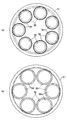
- a disk-shaped susceptor 12 is rotatably provided in a chamber 11, and is provided in each of a plurality of circular openings 12 a formed in the circumferential direction of the outer periphery of the susceptor 12.
- Ring-shaped bearing member 13, disk-shaped soaking plate 14 rotatably mounted on each bearing member 13, and external gear member (spinning susceptor) respectively placed on each soaking plate 14 15, a ring-shaped fixed internal gear member 17 having an internal gear 16 meshing with the external gear member 15, and a substrate 18 held on the surface of the external gear member 15 are heated from the back side of the susceptor 12.
- a heating means (heater) 19 and a flow channel 20 for introducing a source gas in a direction parallel to the surface of the substrate 18 are provided.
- a hollow shaft member 21 extending downward from the susceptor 12 and penetrating the bottom plate 11a of the chamber 11 is provided.
- the inside of the hollow shaft member 21 serves as a source gas passage.
- a driving means (not shown) for rotating the susceptor 12 via the hollow shaft member 21 is provided below the hollow shaft member 21.
- a gas introduction part 22 for introducing a raw material gas into the flow channel 20 is provided at the upper end of the hollow shaft member 21, and a plurality of gas discharge parts 23 are provided on the outer periphery of the flow channel 20. ing.
- the bearing member 13 is formed in an L-shaped cross section having a rising portion 13a on the outer peripheral portion, and corresponds to an upward locking step portion 12b provided on the opening edge of the circular opening 12a on the outer periphery of the lower surface.
- a downward locking step portion 13b is provided.
- a circumferential groove 13d for holding a plurality of rolling members (balls) 13c is provided on the upper surface on the inner peripheral side of the rising portion 13a.
- the heat equalizing plate 14 has a ring-shaped accommodation groove 14a for accommodating the bearing member 13 in the circumferential direction of the lower surface outer circumferential portion, and an upward direction for placing the external gear member 15 on the outer circumferential portion. It has a locking step 14b. Furthermore, a small protrusion 14c is provided in a ring shape on the outer peripheral portion of the upper surface, and a circular concave portion 14d surrounded by the small protrusion 14c is formed on the inner peripheral side of the small protrusion 14c. .
- the external gear member 15 is provided with a ring-shaped external gear portion 15 a on the outer peripheral portion of the lower surface, and the inner diameter and height (thickness) of the external gear portion 15 a correspond to the locking step portion 14 b of the heat equalizing plate 14. It is formed in the dimension. Further, a concave portion 15 b for holding the substrate 18 is provided on the upper surface of the external gear member 15.
- the outer diameter A of the bearing member 13 and the gear reference circular diameter B of the outer gear portion 15 a of the outer gear member 15 are set to be smaller than the outer diameter C of the substrate 18. That is, by providing the external gear portion 15 a on the outer peripheral portion of the lower surface of the external gear member 15 that holds the substrate 18 and with the tip circle positioned on the inner peripheral side of the outer peripheral edge of the external gear member 15, In the gear member 15, the outer peripheral portion of the substrate holding portion 15 b provided on the surface side of the external gear member 15 has the maximum outer diameter of the external gear member 15.
- a small protrusion piece 14c is provided on the outer peripheral portion of the upper surface of the heat equalizing plate 14, and a concave portion 14d is formed on the inner peripheral side of the small protrusion piece 14c.
- a soaking space 24 for equalizing the temperature of the external gear member 15, that is, the surface temperature of the substrate 18 held on the upper surface of the external gear member 15. Can be formed.
- the shape, structure, material, etc. of the external gear member 15, soaking plate 14 and bearing member 13 are different from each other via the heating means 19 below.
- the amount of heat transferred to the substrate 18 can be made uniform, the temperature distribution on the surface of the substrate 18 can be reduced, and the semiconductor thin film formed on the surface of the substrate 18 can be made uniform.
- the composition stability condition range during crystal growth is extremely narrow, and the light emitting layer is most sensitive to the growth temperature. Therefore, it is desirable to reduce the temperature distribution on the surface of the substrate 18, that is, to grow the InGaN thin film at a uniform substrate temperature.
- the temperature distribution is measured in a state where each member is manufactured and assembled, and the depth of the concave portion 14d with respect to the small protrusion 14c and the surface state of the concave portion 14d are adjusted to optimize the soaking space portion 24.
- the temperature difference between a plurality of substrates processed simultaneously can be eliminated.
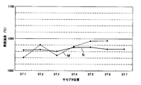
- FIG. 5 shows an example of the result of measuring the temperature distribution on the upper surface of the external gear member 15 corresponding to the center of the substrate 18 (the surface in contact with the substrate 18).
- the temperature distribution in the case where the soaking space portion 24 is not provided has a temperature difference of 5.3 ° C. as indicated by the line M, but the temperature distribution in the case where the soaking space portion 24 is provided is a line.
- the temperature difference is 1.3 ° C., and it can be seen that the temperature difference can be reduced by the soaking space 24.
- the temperature of the upper surface of the external gear member 15 corresponding to two points that are ⁇ 30 mm away from the center of the substrate 18 at each susceptor position is also measured.
- the temperature difference between the upper surface of the external gear member 15 corresponding to two points that are separated from each other by ⁇ 30 mm from the center of the substrate 18 is about 2 ° C. at maximum, and the temperature uniformity of each substrate is maintained.
Landscapes
- Chemical & Material Sciences (AREA)
- General Chemical & Material Sciences (AREA)
- Chemical Kinetics & Catalysis (AREA)
- Engineering & Computer Science (AREA)
- Materials Engineering (AREA)
- Mechanical Engineering (AREA)
- Metallurgy (AREA)
- Organic Chemistry (AREA)
- Led Devices (AREA)
- Chemical Vapour Deposition (AREA)
Abstract
Description
Claims (4)
- チャンバー内に回転可能に設けられた円盤状のサセプタと、該サセプタの外周部周方向に形成された複数の円形開口内にそれぞれ設けられたリング状の軸受部材と、各軸受部材上にそれぞれ回転可能に載置された円盤状の均熱板と、各均熱板上にそれぞれ載置された外歯車部材と、該外歯車部材に噛合する内歯車を備えたリング状の固定内歯車部材と、前記外歯車部材の表面に保持された基板を前記サセプタの裏面側から加熱する加熱手段と、前記基板の表面に平行な方向に原料ガスを導くフローチャンネルとを備えた自公転機構を有する横形気相成長装置であって、前記軸受部材の外径を前記基板の外径より小さい寸法とした気相成長装置。
- チャンバー内に回転可能に設けられた円盤状のサセプタと、該サセプタの外周部周方向に設けられた複数の円形開口内にそれぞれ設けられたリング状の軸受部材と、各軸受部材上にそれぞれ回転可能に載置された円盤状の均熱板と、各均熱板上にそれぞれ載置された外歯車部材と、該外歯車部材に噛合する内歯車を備えたリング状の固定内歯車部材と、前記外歯車部材の表面に保持された基板を前記サセプタの裏面側から加熱する加熱手段と、前記基板の表面に平行な方向に原料ガスを導くフローチャンネルとを備えた自公転機構を有する横形気相成長装置であって、前記外歯車部材の歯車基準円直径を前記基板の外径より小さい寸法とした気相成長装置。
- 前記均熱板と外歯車部材との間に、均熱空間部が設けられている請求項1又は2記載の気相成長装置。
- 前記基板の表面に窒化物系化合物半導体薄膜を成長させる請求項1乃至3のいずれか1項記載の気相成長装置。
Priority Applications (2)
| Application Number | Priority Date | Filing Date | Title |
|---|---|---|---|
| CN201080022518.5A CN102439698B (zh) | 2009-05-22 | 2010-05-14 | 气相生长装置 |
| US13/318,890 US20120048198A1 (en) | 2009-05-22 | 2010-05-14 | Vapor phase growth apparatus |
Applications Claiming Priority (2)
| Application Number | Priority Date | Filing Date | Title |
|---|---|---|---|
| JP2009-123662 | 2009-05-22 | ||
| JP2009123662A JP5436043B2 (ja) | 2009-05-22 | 2009-05-22 | 気相成長装置 |
Publications (1)
| Publication Number | Publication Date |
|---|---|
| WO2010134471A1 true WO2010134471A1 (ja) | 2010-11-25 |
Family
ID=43126152
Family Applications (1)
| Application Number | Title | Priority Date | Filing Date |
|---|---|---|---|
| PCT/JP2010/058185 Ceased WO2010134471A1 (ja) | 2009-05-22 | 2010-05-14 | 気相成長装置 |
Country Status (6)
| Country | Link |
|---|---|
| US (1) | US20120048198A1 (ja) |
| JP (1) | JP5436043B2 (ja) |
| KR (1) | KR101650837B1 (ja) |
| CN (1) | CN102439698B (ja) |
| TW (1) | TWI497570B (ja) |
| WO (1) | WO2010134471A1 (ja) |
Cited By (2)
| Publication number | Priority date | Publication date | Assignee | Title |
|---|---|---|---|---|
| JP2012153927A (ja) * | 2011-01-25 | 2012-08-16 | Sharp Corp | 回転支持構造を有する成膜装置 |
| US20130298836A1 (en) * | 2011-02-03 | 2013-11-14 | Tn Emc Ltd. | Vapor phase growth apparatus |
Families Citing this family (11)
| Publication number | Priority date | Publication date | Assignee | Title |
|---|---|---|---|---|
| CN102485935B (zh) * | 2010-12-06 | 2013-11-13 | 北京北方微电子基地设备工艺研究中心有限责任公司 | 均热板及应用该均热板的基片处理设备 |
| US20130305992A1 (en) * | 2011-02-04 | 2013-11-21 | Micro System Co., Ltd. | Rotating and holding apparatus for semiconductor substrate and conveying apparatus of rotating and holding apparatus for semiconductor substrate |
| JP2012227231A (ja) * | 2011-04-15 | 2012-11-15 | Japan Pionics Co Ltd | Iii族窒化物半導体の気相成長装置 |
| CN103834926A (zh) * | 2012-11-22 | 2014-06-04 | 上海法德机械设备有限公司 | 真空镀膜工件转台 |
| JP6013155B2 (ja) * | 2012-11-28 | 2016-10-25 | 大陽日酸株式会社 | 気相成長装置 |
| JP2015056635A (ja) * | 2013-09-13 | 2015-03-23 | 株式会社東芝 | 気相成長装置及び気相成長方法 |
| US9748113B2 (en) | 2015-07-30 | 2017-08-29 | Veeco Intruments Inc. | Method and apparatus for controlled dopant incorporation and activation in a chemical vapor deposition system |
| JP6661437B2 (ja) * | 2016-03-29 | 2020-03-11 | 大陽日酸株式会社 | 気相成長装置 |
| CN106987899B (zh) * | 2016-10-31 | 2021-08-31 | 姜全忠 | 使用气相传输的材料生长装置、生长方法以及检测装置 |
| JP6763321B2 (ja) * | 2017-03-01 | 2020-09-30 | 東京エレクトロン株式会社 | 自転検出用冶具、基板処理装置及び基板処理装置の運転方法 |
| TWM597506U (zh) | 2018-04-13 | 2020-06-21 | 美商維高儀器股份有限公司 | 具有多區域噴射器塊的化學氣相沉積設備 |
Citations (4)
| Publication number | Priority date | Publication date | Assignee | Title |
|---|---|---|---|---|
| JPH04313220A (ja) * | 1991-04-10 | 1992-11-05 | Sumitomo Electric Ind Ltd | 有機金属気相成長装置 |
| JP2003347228A (ja) * | 2002-05-30 | 2003-12-05 | Renesas Technology Corp | 半導体装置の製造方法および熱処理装置 |
| JP2006114547A (ja) * | 2004-10-12 | 2006-04-27 | Hitachi Cable Ltd | 気相成長装置 |
| JP2008308747A (ja) * | 2007-06-15 | 2008-12-25 | Sumitomo Electric Ind Ltd | 気相成長装置および気相成長方法 |
Family Cites Families (6)
| Publication number | Priority date | Publication date | Assignee | Title |
|---|---|---|---|---|
| JPH02130922A (ja) * | 1988-11-11 | 1990-05-18 | Toshiba Corp | 半導体基板エッチング装置 |
| JP4537566B2 (ja) * | 2000-12-07 | 2010-09-01 | 大陽日酸株式会社 | 基板回転機構を備えた成膜装置 |
| JP2003224074A (ja) * | 2002-01-29 | 2003-08-08 | Hitachi Cable Ltd | 気相エピタキシャル成長方法及びその装置並びにそれに用いられる均熱板 |
| CN1865495A (zh) * | 2005-05-20 | 2006-11-22 | 中国科学院半导体研究所 | 金属有机物化学气相淀积设备反应室中的公转自转机构 |
| JP2007042899A (ja) * | 2005-08-03 | 2007-02-15 | Hitachi Cable Ltd | 気相成長装置 |
| JP4706531B2 (ja) | 2006-03-27 | 2011-06-22 | 日立電線株式会社 | 気相成長装置 |
-
2009
- 2009-05-22 JP JP2009123662A patent/JP5436043B2/ja active Active
-
2010
- 2010-05-14 US US13/318,890 patent/US20120048198A1/en not_active Abandoned
- 2010-05-14 WO PCT/JP2010/058185 patent/WO2010134471A1/ja not_active Ceased
- 2010-05-14 CN CN201080022518.5A patent/CN102439698B/zh active Active
- 2010-05-14 KR KR1020117030366A patent/KR101650837B1/ko active Active
- 2010-05-21 TW TW099116272A patent/TWI497570B/zh active
Patent Citations (4)
| Publication number | Priority date | Publication date | Assignee | Title |
|---|---|---|---|---|
| JPH04313220A (ja) * | 1991-04-10 | 1992-11-05 | Sumitomo Electric Ind Ltd | 有機金属気相成長装置 |
| JP2003347228A (ja) * | 2002-05-30 | 2003-12-05 | Renesas Technology Corp | 半導体装置の製造方法および熱処理装置 |
| JP2006114547A (ja) * | 2004-10-12 | 2006-04-27 | Hitachi Cable Ltd | 気相成長装置 |
| JP2008308747A (ja) * | 2007-06-15 | 2008-12-25 | Sumitomo Electric Ind Ltd | 気相成長装置および気相成長方法 |
Cited By (2)
| Publication number | Priority date | Publication date | Assignee | Title |
|---|---|---|---|---|
| JP2012153927A (ja) * | 2011-01-25 | 2012-08-16 | Sharp Corp | 回転支持構造を有する成膜装置 |
| US20130298836A1 (en) * | 2011-02-03 | 2013-11-14 | Tn Emc Ltd. | Vapor phase growth apparatus |
Also Published As
| Publication number | Publication date |
|---|---|
| CN102439698A (zh) | 2012-05-02 |
| CN102439698B (zh) | 2014-10-22 |
| KR101650837B1 (ko) | 2016-08-24 |
| TWI497570B (zh) | 2015-08-21 |
| JP2010272708A (ja) | 2010-12-02 |
| US20120048198A1 (en) | 2012-03-01 |
| KR20120024798A (ko) | 2012-03-14 |
| TW201108303A (en) | 2011-03-01 |
| JP5436043B2 (ja) | 2014-03-05 |
Similar Documents
| Publication | Publication Date | Title |
|---|---|---|
| JP5436043B2 (ja) | 気相成長装置 | |
| JP5092975B2 (ja) | エピタキシャルウェーハの製造方法 | |
| US8685855B2 (en) | Tray for CVD and method for forming film using same | |
| US20100282170A1 (en) | Vapor phase growth susceptor and vapor phase growth apparatus | |
| US20120321788A1 (en) | Rotation system for thin film formation | |
| JP6101591B2 (ja) | エピタキシャルウェハの製造装置および製造方法 | |
| JP2005260095A (ja) | エピタキシャル成長装置 | |
| JP5139105B2 (ja) | 気相成長装置 | |
| TWI559440B (zh) | 晶圓承載裝置 | |
| US8038793B2 (en) | Epitaxial growth method | |
| JP2018107289A (ja) | サセプタ、気相成長装置及び気相成長方法 | |
| JP5139107B2 (ja) | 気相成長装置 | |
| JP5432041B2 (ja) | 気相成長装置 | |
| JP5292963B2 (ja) | 成膜装置およびそれを用いた製造方法 | |
| TW201406983A (zh) | 承載器及氣相成長裝置 | |
| JP2013004956A (ja) | 薄膜形成のための回転システム及びその方法 | |
| JP5215033B2 (ja) | 気相成長方法 | |
| JP2009275255A (ja) | 気相成長装置 | |
| KR102727620B1 (ko) | 기판지지부 | |
| JP2011187695A (ja) | 気相成長方法 | |
| KR101238842B1 (ko) | 반도체 제조용 서셉터 및 이를 포함한 에피택셜 성장 장치 | |
| JP6732483B2 (ja) | 基板保持部材及び気相成長装置 | |
| US20120321790A1 (en) | Rotation system for thin film formation | |
| JP4720692B2 (ja) | 気相成長用サセプタ、気相成長装置及び気相成長方法 | |
| JP2011192731A (ja) | 気相成長装置 |
Legal Events
| Date | Code | Title | Description |
|---|---|---|---|
| WWE | Wipo information: entry into national phase |
Ref document number: 201080022518.5 Country of ref document: CN |
|
| 121 | Ep: the epo has been informed by wipo that ep was designated in this application |
Ref document number: 10777704 Country of ref document: EP Kind code of ref document: A1 |
|
| WWE | Wipo information: entry into national phase |
Ref document number: 13318890 Country of ref document: US |
|
| NENP | Non-entry into the national phase |
Ref country code: DE |
|
| ENP | Entry into the national phase |
Ref document number: 20117030366 Country of ref document: KR Kind code of ref document: A |
|
| 122 | Ep: pct application non-entry in european phase |
Ref document number: 10777704 Country of ref document: EP Kind code of ref document: A1 |