WO2010134285A1 - プリント配線板およびプリント配線板の製造方法 - Google Patents
プリント配線板およびプリント配線板の製造方法 Download PDFInfo
- Publication number
- WO2010134285A1 WO2010134285A1 PCT/JP2010/003190 JP2010003190W WO2010134285A1 WO 2010134285 A1 WO2010134285 A1 WO 2010134285A1 JP 2010003190 W JP2010003190 W JP 2010003190W WO 2010134285 A1 WO2010134285 A1 WO 2010134285A1
- Authority
- WO
- WIPO (PCT)
- Prior art keywords
- wiring
- mask
- covering portion
- substrate
- wiring board
- Prior art date
- Legal status (The legal status is an assumption and is not a legal conclusion. Google has not performed a legal analysis and makes no representation as to the accuracy of the status listed.)
- Ceased
Links
Images





Classifications
-
- H—ELECTRICITY
- H05—ELECTRIC TECHNIQUES NOT OTHERWISE PROVIDED FOR
- H05K—PRINTED CIRCUITS; CASINGS OR CONSTRUCTIONAL DETAILS OF ELECTRIC APPARATUS; MANUFACTURE OF ASSEMBLAGES OF ELECTRICAL COMPONENTS
- H05K1/00—Printed circuits
- H05K1/02—Details
- H05K1/11—Printed elements for providing electric connections to or between printed circuits
- H05K1/115—Via connections; Lands around holes or via connections
-
- H—ELECTRICITY
- H05—ELECTRIC TECHNIQUES NOT OTHERWISE PROVIDED FOR
- H05K—PRINTED CIRCUITS; CASINGS OR CONSTRUCTIONAL DETAILS OF ELECTRIC APPARATUS; MANUFACTURE OF ASSEMBLAGES OF ELECTRICAL COMPONENTS
- H05K2201/00—Indexing scheme relating to printed circuits covered by H05K1/00
- H05K2201/09—Shape and layout
- H05K2201/09209—Shape and layout details of conductors
- H05K2201/09654—Shape and layout details of conductors covering at least two types of conductors provided for in H05K2201/09218 - H05K2201/095
- H05K2201/09672—Superposed layout, i.e. in different planes
Definitions
- the present invention relates to a printed wiring board and a method for manufacturing the printed wiring board.
- a through hole (hole) 901A is formed in a substrate, and copper is plated inside the hole 901A, thereby providing wiring provided on the front and back surfaces of the substrate 901.
- the connection between the terminals 903 is established (in FIG. 12, only the wiring 903 provided on the surface of the substrate 901 is shown, see Patent Document 1).
- a printed wiring board is manufactured by the following manufacturing method. First, a substrate having copper foil provided on both sides is prepared, and a through hole 901A is formed at a predetermined location by a drill or a laser.
- the copper foil is etched into a predetermined pattern to form a wiring 903.
- a circular region called a land 904 is provided in a portion overlapping with the through hole 901A.
- the diameter of the land 904 is larger than the wiring width of the wiring 903.
- plating 902 is applied in the through hole 901A to establish electrical connection between the wirings.
- the conventional method has the following problems.
- the diameter of the land 904 is larger than the wiring width of the wiring 903. This is because even when the land 904 and the wiring 903 are formed at positions shifted from desired positions, the land 904 overlaps the through hole 901A, and the plating 902 and the wiring 903 formed in the through hole 901A. This is so that the continuity can be obtained.
- the diameter of the land 904 is determined in consideration of the positional deviation, it is difficult to make the land 904 smaller than a predetermined size. Therefore, it is difficult to improve the wiring density in the printed wiring board having such a configuration.
- the present invention is to provide a printed wiring board and a method for manufacturing the printed wiring board that can cope with an improvement in wiring density.
- the substrate includes a substrate, a first wiring provided on the front surface of the substrate, and a second wiring provided on the back surface of the substrate, and the substrate penetrates the substrate.
- a connecting portion for connecting the first wiring and the second wiring is provided, and in the plan view from the substrate surface side, the connecting portion is between a pair of sides along the wiring extending direction of the first wiring.
- the connection surface connected to the first wiring of the connection portion is connected to the first wiring so that it does not protrude from the first wiring, and the connection portion extends along the wiring extending direction of the second wiring.
- a printed wiring board is provided that spans between a pair of sides and is connected to the second wiring so that a connection surface connected to the second wiring of the connecting portion does not protrude from the second wiring.
- the connecting portion spans between a pair of sides along the wiring extending direction of the first wiring, and the first wiring side connection surface of the connecting portion does not protrude from the first wiring.
- the connection part spans between a pair of sides along the wiring extension direction of the second wiring, and is connected to the second wiring so that the connection surface on the second wiring side of the connection part does not protrude from the second wiring.
- the connection surface on the first wiring side of the connection part does not protrude from the first wiring, and the connection surface on the second wiring side does not protrude from the second wiring.
- the wiring density can be improved and the wiring density can be improved. Therefore, the wiring density can be improved as compared with the conventional case where lands larger than the wiring width are formed on the substrate.
- connection portion is provided so as not to protrude from a region where the first wiring and the second wiring overlap in a plan view from the substrate surface side.
- the length along the wiring width direction of the first wiring of the connection surface connected to the first wiring of the connection part is the same as the wiring width of the first wiring, and the second of the connection part
- the length of the connection surface connected to the wiring along the wiring width direction of the second wiring is preferably the same as the wiring width of the second wiring.
- the wiring width of the portion connected to the connection portion of the first wiring and the wiring width of the portion connected to the connection portion of the second wiring are substantially equal, Match the wiring width direction of the portion connected to the connecting portion and the wiring width direction of the portion connected to the connecting portion of the second wiring, and the first wiring among the first wiring as viewed from the substrate surface side.
- the portion connected to the connecting portion and the portion connected to the connecting portion of the second wiring one is connected to the connecting portion of the first wiring so as not to protrude from the other in the wiring width direction Of the portion to be connected and the portion of the second wiring, it is preferable that portions connected to the connection portion overlap each other. By doing so, the wiring density can be further improved.
- a plurality of the first wiring, the second wiring, and the connection portions are provided, and the plurality of connection portions are arranged on a substantially straight line when viewed from the substrate surface side, and have a hole between adjacent connection portions. Is preferably formed.
- the substrate is formed with a slit that penetrates the substrate and extends in a predetermined direction when viewed from the substrate surface side, and the plurality of connecting portions are separated from each other by a predetermined interval. It is preferable to be formed so as to be embedded.
- the printed wiring board having such a configuration is excellent in manufacturing stability.
- first wiring and one end of the second wiring overlap, and the first wiring and the second wiring extend in opposite directions, and one end of the first wiring
- the length dimension in the extending direction of the first wiring and the second wiring in the region where the end and one end of the second wiring overlap each other is the length of the first wiring and the second wiring of the connection portion. It is preferably longer than the length dimension along the extending direction.
- the printed wiring board having such a configuration is excellent in manufacturing stability.
- a manufacturing method for manufacturing the above-described printed wiring board can also be provided. That is, an insulating layer, a first wiring provided on one surface of the insulating layer, a second wiring provided on the other surface of the insulating layer, and the first wiring provided in the insulating layer
- a printed wiring board including a connection portion for connecting the second wiring, an insulating layer, a first conductor layer provided so as to cover one surface of the insulating layer, and the other of the insulating layers
- An opening is formed on one conductor layer, and a first mask having a covering portion corresponding to the wiring shape of the first wiring is provided, and an opening is formed on the second conductor layer, Provide a second mask with a covering part according to the wiring shape of the two wirings Selectively removing the exposed
- the alignment accuracy between the first mask and the second mask is high.
- the positional deviation between the first mask and the second mask and the substrate is likely to occur. Since the substrate is subject to dimensional variations, the accuracy of alignment becomes unclear. Particularly in the flexible wiring board, the dimensional variation is remarkable.
- the present invention has been made in view of this point.
- a part of the covering portion of the first mask for forming the first wiring and a part of the conductive member overlap, and a part of the conductive member and the second wiring are arranged.
- Each mask is arranged so that a part of the covering portion of the second mask to be formed overlaps, and the conductive member extends in a direction orthogonal to the substrate thickness direction. Therefore, in the alignment of the substrate with the first mask for forming the first wiring and the second mask for forming the second wiring, the positions of the first mask and the second mask are aligned with the substrate. On the other hand, even if the conductive member is displaced in the extending direction, the conductive member exists between the first mask and the second mask.
- the manufacturing method of the present invention it is possible to improve the wiring density of the printed wiring board.
- a part of the covering part of the first mask for forming the first wiring and a part of the conductive member overlap and a covering part of the second mask for forming the second wiring.
- the first mask and the second mask may be arranged so that a part of the conductive member and the other part of the conductive member overlap each other, but in order to form the first wiring as viewed from the substrate surface side A portion of the covering portion of the first mask overlaps with a portion of the conductive member, and a portion of the covering portion of the second mask for forming the second wiring and the conductive member It is preferable to provide the first mask and the second mask so as to overlap the part.
- the conductive member remains part of the first mask covering part and part of the second mask covering part, and the first mask opening and the first mask. Another region exposed from the opening of the second mask can be selectively removed to form a connection portion. Therefore, the connection part can be formed so as to hardly protrude from the region where the first wiring and the second wiring overlap.
- the covering portion of the first mask and the covering portion of the second mask each have regions having the same width dimension,
- the width direction of the region of the mask covering portion coincides with the width direction of the region of the second mask covering portion, and one of the regions is widthwise from the other region when viewed from the substrate surface side.
- the area of the covering portion of the first mask and the area of the covering portion of the second mask are overlapped with each other so as not to protrude from the substrate surface side.
- the region of the covering portion and the region of the covering portion of the second mask pass through the overlapping portion, and the width direction of the region of the covering portion of the first mask and the covering portion of the second mask For the direction perpendicular to the width direction of the region It is preferable that the conductive member so as to intersect extends.
- the width dimension of the covering portion of the first mask is a dimension corresponding to the wiring width of the first wiring.
- the width dimension of the covering portion of the second mask is a dimension corresponding to the wiring width of the second wiring.
- the covering portion of the first mask and the covering portion of the second mask are arranged so as to be greatly shifted in the width direction when viewed from the substrate surface side, and a greatly shifted region (for example, the covering of the first mask)
- the first wiring or the second wiring is removed when the conductive member is removed. Wiring may also be removed.
- the covering portion of the first mask and the covering portion of the second mask each have regions having the same width dimension, and the width direction of the region of the covering portion of the first mask
- the first mask so that the width direction of the region of the covering portion of the second mask coincides and one region does not protrude from the other region in the width direction when viewed from the substrate surface side.
- the region of the covering portion and the region of the covering portion of the second mask are overlapped.
- the width of the region of the first mask covering portion passes through the portion where the region of the first mask covering portion and the region of the second mask covering portion overlap each other.
- the conductive member extends so as to intersect the direction and the direction orthogonal to the width direction of the region of the covering portion of the second mask. Therefore, when removing a part of the conductive member, it is possible to prevent the removal of a part of the first wiring or a part of the second wiring, and the first wiring and the second wiring. Wiring can be reliably formed with a desired wiring width.
- the region of the covering portion of the first mask and the second mask so that one region does not protrude in the width direction from the other region as viewed from the substrate surface side overlap the region of the covering portion means that when the masks are aligned, the region of the covering portion of the first mask and the region of the covering portion of the second mask are almost protruded from each other. This includes superposition so that there is a slight shift due to the alignment accuracy of the alignment apparatus.
- the conductive member may overlap the covering portion of the first mask and the covering portion of the second mask as viewed from the substrate surface side. And extending across the overlapping region, intersecting the overlapping region, and in other regions so as not to overlap the covering portion of the first mask and the covering portion of the second mask. It is preferable to provide the first mask and the second mask. By providing the first mask and the second mask in this manner, it is possible to prevent the first wiring or the second wiring from being removed when the conductive member is removed. It should be noted that, here, “the first mask and the second mask so that the conductive member does not overlap the covering portion of the first mask and the covering portion of the second mask in another region”.
- Providing a mask '' means that the conductive member is a region other than a region where the covering portion of the first mask and the covering portion of the second mask overlap each other, and the covering portion of the first mask and , which means that it hardly overlaps with the covering portion of the second mask. Accordingly, due to the alignment accuracy of the apparatus, a slight shift occurs between the masks, and the conductive member is slightly outside the area where the covering portion of the first mask and the covering portion of the second mask overlap. In other words, it overlaps with the first mask and the second mask.
- connection portion a plurality of the first wiring, the second wiring, and the connection portion are formed, and the conductive member is selectively removed to form a plurality of spaced connection portions.
- one end portion of the covering portion of the first mask and one end portion of the covering portion of the second mask overlap each other. And forming the first mask and the second mask so that the covering portion of the first mask and the covering portion of the second mask extend in different directions, and the conductive member is , One end of the covering portion of the first mask intersects with a region where one end of the covering portion of the second mask overlaps, and the covering portion of the first mask.
- the length dimension in a direction orthogonal to the extending direction of the conductive member in a region where the one end portion of the second mask and the one end portion of the covering portion of the second mask overlap each other is It is preferable that the length is longer than the length in the direction orthogonal to the extending direction.
- the length in the direction orthogonal to the extending direction of the conductive member in the region where one end of the covering portion of the first mask and one end of the covering portion of the second mask overlap.
- the dimension is longer than the length dimension in the direction orthogonal to the extending direction of the conductive member. Therefore, even if the first mask and the second mask are arranged at positions shifted in the direction orthogonal to the extending direction of the conductive member with respect to the substrate, the first mask covering portion and the second mask It is possible to ensure the overlap between the conductive member and the region where the mask covering portion overlaps.
- the printed wiring board is preferably a flexible wiring board.
- a printed wiring board can be provided by the manufacturing method as described above.
- a printed wiring board that can cope with an improvement in wiring density and a method for manufacturing the same are provided.
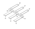
- FIG. 1 is a perspective view of a main part of the printed wiring board 1.
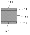
- FIG. 2 illustrates only the first wiring 12, the connection portion 14, and the second wiring 13 of the printed wiring board 1
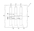
- FIG. 3 is a plan view of the main part of the printed wiring board 1.
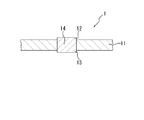
- 10 is a cross-sectional view in the xx direction of FIG.
- the printed wiring board 1 includes a substrate 11, a plurality of first wires 12 provided on the front surface of the substrate 11, and a plurality of second wires 13 provided on the back surface of the substrate 11.
- the substrate 11 is provided with a connection portion 14 that penetrates the substrate 11 and connects the first wiring 12 and the second wiring 13.
- the connection portion 14 spans between a pair of sides along the wiring extending direction of the first wiring 12, and the first wiring of the connection portion 14 in the plan view from the substrate surface side. 12 is connected to the first wiring 12 so that the connection surface 141 connected to the first wiring 12 does not protrude from the first wiring 12.
- the connection portion 14 extends between a pair of sides along the wiring extending direction of the second wiring 13 and is connected to the second wiring 13 of the connection portion 14 in a plan view from the substrate surface side.
- 142 is connected to the second wiring 13 so as not to protrude from the second wiring 13.
- the printed wiring board 1 of this embodiment is a flexible wiring board.
- the substrate 11 is an insulating substrate having an insulating layer made of, for example, polyimide resin or polyethylene resin. Although not shown, wiring and the like are formed inside the substrate 11.
- a plurality of connection portions 14 are embedded in the substrate 11.
- the connection part 14 is an electroconductive member, for example, is a metal such as copper.
- the connection portions 14 penetrate the front and back surfaces of the substrate 11 and are spaced apart from each other.
- the plurality of connecting portions 14 are arranged substantially in a straight line in a direction intersecting with the extending direction of the first wiring 12 and the extending direction of the second wiring 13 (a direction orthogonal in the present embodiment).
- Each connection portion 14 is formed in a through hole (slit 111) that penetrates the substrate 11. As shown in FIG.
- connection surface 141 of the connection portion 14 is connected to the first wiring 12, and the connection surface 141 does not protrude from the first wiring 12 in plan view on the substrate surface side.
- the connection surface 141 is a surface that is flush with the opening on the first wiring 12 side of the through-hole 111 that penetrates the substrate 11 (that is, the surface of the substrate 11).
- connection surface 142 of the connection unit 14 is connected to the second wiring 13, and the connection surface 142 does not protrude from the second wiring 13 in a plan view on the substrate surface side.
- the connection surface 142 is a surface that is flush with the opening on the second wiring 13 side of the through hole 111 that penetrates the substrate 11 (that is, the back surface of the substrate 11).
- connection part 14 is connected to a part of the first wiring 12 (a part connected to the connection part 14 in the first wiring 12) and a part of the second wiring 13 (a connection part 14 in the second wiring 13). Part). As shown in FIG. 3, the connecting portion 14 does not protrude from the region where a part of the first wiring 12 and a part of the second wiring 13 overlap when viewed from the substrate surface side.
- connection portion 14 is connected to the first wiring 12 by the wiring width of the first wiring 12 and is connected to the second wiring 13 by the wiring width of the second wiring 13.
- connection part 14 is a solid rectangular parallelepiped shape. Between each connection part 14, the hole 111A is formed.
- This hole 111 ⁇ / b> A is a through-hole penetrating the substrate 11.
- a pair of opposing side walls of the hole 111 ⁇ / b> A is composed of adjacent connecting portions 14.
- the substrate 11 is formed with a slit 111 that penetrates the substrate 11 and extends in a predetermined direction when viewed from the substrate surface side.
- the connecting portion 14 is arranged at a predetermined interval so as to fill a part of the slit 111.
- connection part 14 becomes hole 111A.
- the inside of the hole 111A may be filled with another insulating resin (for example, a coverlay film) different from the substrate 11, and may not be filled.
- a first wiring 12 is provided on one surface (front surface) of the substrate 11.
- the first wiring 12 is a wiring made of metal such as copper.
- the first wiring 12 has one end connected to the connection portion 14 and is formed to extend in one direction from the connection portion 14. As viewed from the substrate surface side, the end of the first wiring 12 protrudes from the connecting portion 14 to the opposite side of the extending direction of the first wiring 12.
- the width dimension of the connection portion of the first wiring 12 with the connection portion 14 is equal to the width dimension W3 of the connection portion 14.
- the first wiring 12 is formed so that the wiring end including the connection portion with the connection portion 14 does not bulge in the wiring width direction as compared with other regions of the first wiring 12 when viewed from the substrate surface side. .
- a second wiring 13 is provided on the other surface (back surface) of the substrate 11.
- the second wiring 13 is a wiring made of metal such as copper.
- the second wiring 13 is formed so that one end thereof is connected to the connection portion 14 and extends in one direction from the connection portion 14.
- the extending direction of the second wiring 13 from the connecting portion 14 is opposite to the extending direction of the first wiring 12.
- the end of the second wiring 13 is projected from the connection portion 14 to the opposite side of the extending direction of the second wiring 13 when viewed from the substrate surface side, and overlaps the first wiring 12 when viewed from the substrate surface side. Yes.
- the end of the first wiring 12 also overlaps the second wiring 13.
- the width dimension of the connection portion of the second wiring 13 with the connection portion 14 is equal to the width dimension W3 of the connection portion 14.
- connection portion 14 is provided so as not to protrude from the first wiring 12 and the second wiring 13 when viewed from the substrate surface side. Further, the second wiring 13 is formed so that the end including the connection portion with the connection portion 14 does not bulge in the wiring width direction as compared with other regions of the second wiring 13 when viewed from the substrate surface side.
- the length dimension L1 in the extending direction of the first wiring 12 and the second wiring 13 in a region where one end of the first wiring 12 and one end of the second wiring 13 are overlapped is determined by the connection portion.
- the length 14 is longer than the length L2 along the extending direction of the first wiring 12 and the second wiring 13.
- the first wiring 12 and the second wiring 13 as described above are covered with an insulating resin film (coverlay film) (not shown).
- the method for manufacturing the printed wiring board 1 of the present embodiment is provided so as to cover the substrate 11, the first conductor layer 22 provided so as to cover one surface of the substrate 11, and the other surface of the substrate 11.
- the step of providing the first mask 26 and the second mask 27 as viewed from the substrate surface side, a part of the covering portion 261 of the first mask 26 for forming the first wiring 12, and the conductive member 24 and the part of the conductive member 24 and the part of the covering portion 271 of the second mask 27 for forming the second wiring 13 are overlapped with each other.
- One mask 26 and the second mask 27 are provided.
- a substrate 2 is prepared.
- the substrate 2 includes a substrate 11, a first conductor layer 22 provided on the surface of the substrate 11, and a second conductor layer 23 provided on the back surface of the substrate 11.
- a conductive member 24 penetrating the front and back surfaces is embedded in the substrate 2.
- the conductive member 24 serves as a connection portion with the connection portion 14 of the first wiring 12, a connection portion with the connection portion 14 of the second wiring 13, and further the connection portion 14.
- the conductive member 24 is made of metal such as copper.
- the conductive member 24 extends in one direction along a direction orthogonal to the thickness direction of the substrate 2 and has a rectangular parallelepiped shape in the present embodiment. In the present embodiment, the extending direction of the conductive member 24 is a direction orthogonal to the extending directions of the first wiring 12 and the second wiring 13.
- the first conductor layer 22 becomes the first wiring 12 and is, for example, a metal layer such as copper.
- the first conductor layer 22 covers the surface of the substrate 11.
- the second conductor layer 23 becomes the second wiring 13 and is, for example, a metal layer such as copper.
- the second conductor layer 23 covers the back surface of the substrate 11.
- Such a substrate 2 can be manufactured as follows. First, a substrate provided with a substrate 11, a first conductor layer 22 that covers the surface of the substrate 11, and a second conductor layer 23 that covers the back surface of the substrate 11 is prepared. A slit 111 that penetrates the first conductor layer 22, the substrate 11, and the second conductor layer 23 is formed in the substrate, and the slit 111 is embedded by the conductive member 24. The conductive member 24 and the first conductor layer 22 are in contact with each other at the side wall of the slit 111, and the conductive member 24 and the second conductor layer 23 are in contact with each other at the side wall of the slit 111. In addition, when the conductive member 24 is embedded in the slit 111, a plating method is used. For example, electroplating is used.
- the width of the slit 111 (the length in the direction orthogonal to the slit extending direction) is, for example, about 20 ⁇ m.
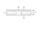
- FIG. 5 is a view showing a cross section along the direction VV in FIG. Thereafter, the resist film 25 is selectively removed to form openings having a predetermined pattern. Specifically, a pattern corresponding to the pattern of the first wiring 12 and the second wiring 13 is left. Specifically, first, an exposure mask is disposed above the resist film 25. Positioning of the exposure mask and the substrate 2 is performed, light is irradiated to the opening portion of the mask, and the irradiated portion is cured. Thereafter, the unirradiated portion is removed with an alkaline solution, and a first mask 26 and a second mask 27 are formed as shown in FIG.
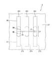
- FIGS. 6 and 7 are cross-sectional views of the substrate 2 provided with the first mask 26 and the second mask 27, and FIG. 7 shows the substrate 2 provided with the first mask 26 and the second mask 27 as a substrate. It is the top view seen from the surface side.
- a part of the covering portion 261 for forming the first wiring 12 of the first mask 26 and a part of the conductive member 24 overlap, and the part of the conductive member 24 and the second mask 27
- the first mask 26 and the second mask 27 are formed so as to overlap a part of the covering portion 271 for forming the second wiring 13. That is, the first mask 26 and the second mask 27 are formed so that a part of the conductive member 24 is sandwiched between a part of the covering part 261 and a part of the covering part 271.
- the covering portion 261 of the first mask 26 and the covering portion 271 of the second mask 27 have regions having the same width dimension. Specifically, as shown in FIG. 7, the width dimension W4 of a partial region (in the present embodiment, the end portion) of the covering portion 261 of the first mask 26 and the covering portion 271 of the second mask 27.
- the width dimension W5 of the partial region (in the present embodiment, the end portion) is substantially equal.
- the width direction of the partial area of the covering portion 261 of the first mask 26 and the partial area of the covering portion 271 of the second mask 27 are made to coincide with each other, and when viewed from the substrate surface side, one is in the width direction from the other. A part of the areas of the covering portions 261 and 271 are overlapped so as not to be exposed.
- the conductive member 24 extends so as to intersect the direction perpendicular to the width direction of the overlapping regions of the covering portions 261 and 271 through the overlapping region of the covering portions 261 and 271. Exists. In the present embodiment, the conductive member 24 extends along the width direction of the overlapping region of the covering portions 261 and 271.
- the conductive member 24 When viewed from the substrate surface side, the conductive member 24 passes through the overlapping region of the covering portion 261 of the first mask 26 and the covering portion 271 of the second mask 27 and intersects the overlapping region. Then, while extending, the covering portion 261 of the first mask 26 and the covering portion 271 of the second mask 27 do not overlap in other regions.
- the covering portion 261 of the first mask 26 when viewed from the substrate surface side, has one end portion that overlaps a part of the conductive member 24 and from the conductive member 24 side in one direction. It is formed to extend.
- the covering portion 271 of the second mask 27 When viewed from the substrate surface side, has one end overlapping with a part of the conductive member 24 and the one direction (covering the first mask 26) from the conductive member 24 side. It extends in the direction opposite to the direction in which the portion near the end of the portion 261 extends.
- one end tip of the covering portion 261 of the first mask 26 protrudes in the extending direction of the covering portion 271 of the second mask 27 from the conductive member 24, and the second end. It overlaps with the covering portion 271 of the mask 27. Further, the end of the end of the second mask 27 protrudes in the extending direction of the covering portion 261 of the first mask 26 from the conductive member 24 and overlaps the covering portion 261 of the first mask 26. In other words, it is orthogonal to the extending direction of the conductive member 24 in the region where one end of the covering portion 261 of the first mask 26 and one end of the covering portion 271 of the second mask 27 overlap.
- the length dimension L4 is longer than the length dimension L5 in the direction orthogonal to the extending direction of the conductive member 24.
- the alignment accuracy between the first mask 26 and the second mask 27 is high.
- the first conductor layer 22 exposed from the opening of the first mask 26 and the second conductor layer 23 exposed from the opening of the second mask 27 are removed by etching, and the opening of the first mask and The conductive member 24 exposed from the opening of the second mask is selectively removed.
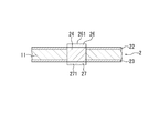
- the substrate 2 is immersed in an etchant and wet etching is performed. Note that a region of the conductive member 24 that is not covered by the first mask 26 and the second mask 27 is removed by etching, and becomes a hole 111 ⁇ / b> A penetrating the substrate 11.
- the printed wiring board 1 can be obtained by the processes as described above.
- a part of the covering portion 261 of the first mask 26 for forming the first wiring 12 and a part of the conductive member 24 overlap, and a part of the conductive member 24,
- Each mask is arranged so that a part of the covering portion 271 of the second mask 27 for forming the second wiring 13 overlaps.
- the conductive member 24 extends in a direction orthogonal to the thickness direction of the substrate 2.
- the first mask 26 and the second mask 27 for forming the second wiring 13 Even if the position of the mask 27 is shifted in the extending direction of the conductive member 24 with respect to the substrate 2, the conductive member 24 is between the covering portion 261 of the first mask 26 and the covering portion 271 of the second mask 27. Will exist. Thereby, the electrical connection between the first wiring 12 and the second wiring 13 can be reliably ensured.
- the conductive member 24 it is possible to allow a positional shift between the first mask 26, the second mask 27, and the substrate 2, so that the conductive material formed on the mask and the substrate as in the past is used. Therefore, it is not necessary to form a land wider than the wiring at the end of the wiring in consideration of the positional deviation from the through hole.
- the length L4 is longer than the length L5 of the conductive member 24.
- the substrate 2 or the exposure mask is moved in two orthogonal directions (x-axis direction, The position is adjusted by moving in the rotation direction about the rotation axis about the y-axis direction) or the ⁇ -axis (axis orthogonal to the x-axis and y-axis in FIG. 3). Therefore, in general, the masks 26 and 27 are often displaced in the rotation direction about the x-axis direction, the y-axis direction, and the ⁇ -axis with respect to the substrate 2, but according to the manufacturing method of this embodiment, The positional deviation of the masks 26 and 27 with respect to the substrate 2 can be allowed with certainty.
- connection portion 14 is connected between the first wiring 12 and the second wiring 13. It is possible to connect the first mask 26, the second mask 27, and the substrate 2 with a positional deviation. For this reason, in the present embodiment, it is not necessary to form a land wider than the wiring at the end portion of the wiring in consideration of the positional deviation between the mask and the substrate as in the prior art.
- connection portion 14 spans between a pair of sides along the wiring extending direction of the first wiring 12, and the connection surface 141 on the first wiring 12 side of the connection portion 14 does not protrude from the first wiring 12. It is connected to the first wiring 12. Further, the connecting portion 14 spans between a pair of sides along the wiring extending direction of the second wiring 13, and the connecting surface 142 on the second wiring 13 side of the connecting portion 14 does not protrude from the second wiring 13. Are connected to the second wiring 13. By doing in this way, it becomes possible to form another wiring adjacent to the 1st wiring 12 or the 2nd wiring 13, and it can improve wiring density.
- connection portion 14 is provided so as not to protrude from the region where the first wiring 12 and the second wiring 13 overlap, and extends along the wiring extending direction of the first wiring 12.
- the second wiring 13 is disposed so as to span between a pair of sides along the wiring extending direction of the second wiring 13. That is, the connection portion 14 is provided without protruding from the wiring width of the first wiring 12 and the wiring width of the second wiring 13. Accordingly, it is possible to improve the wiring density as compared with the conventional case where a land larger than the wiring width is formed.
- connection part with the connection part 14 of the 1st wiring 12 is the same wiring width as the other area
- connection portion of the second wiring 13 with the connection portion 14 has the same wiring width as other regions of the second wiring 13 and does not bulge.
- the improvement of the wiring density of a printed wiring board can be aimed at reliably.
- a part of the wiring width direction of the first wiring 12 is matched with a part of the wiring width direction of the second wiring 13, and one is viewed from the other side in the wiring width direction.
- a part of the first wiring 12 and a part of the second wiring 13 overlap each other so as not to protrude.
- the improvement of the wiring density of a printed wiring board can be aimed at reliably.
- the connecting portion 14 is formed along the width direction of the first wiring 12 and the width direction of the second wiring 13, but not limited to this, as shown in FIG.
- the wiring 12 may extend so as to intersect the width direction of the wiring 12.
- the length dimension W3 along the wiring width direction of the first wiring 12 and the second wiring 13 of the connecting portion 14, the wiring width W1 of the first wiring 12, and the wiring width W2 of the second wiring 13 are equal.
- the printed wiring board 1 is a flexible wiring board.
- the printed wiring board 1 is not limited to this and may be a rigid wiring board or a rigid flexible wiring board.
- the length L4 is longer than the length L5 of the conductive member 24.
- the length L4 is not limited thereto, and L4 and L5 may be the same length.
- the connection part 14 was formed so that it might not protrude from the area
- the connection portion 14 may slightly protrude from the region where the first wiring 12 and the second wiring 13 overlap when viewed from the substrate surface side.
- FIG. 11 corresponds to a cross-sectional view of FIG. 1 viewed from the xx direction.
Landscapes
- Engineering & Computer Science (AREA)
- Microelectronics & Electronic Packaging (AREA)
- Structure Of Printed Boards (AREA)
Abstract
プリント配線板1は、基板11と、基板11の表面に設けられた複数の第一配線12と、基板11の裏面に設けられた複数の第二配線13とを有する。接続部14は、第一配線12の一部および第二配線13の一部間に設けられ、第一配線12の一部および第二配線13の一部が重なりあった領域内からはみださず、接続部14は、基板表面側からの平面視において第一配線12の配線延在方向に沿った一対の辺間にまたがるとともに、第二配線13の配線延在方向に沿った一対の辺間にまたがるように配置されている。
Description
本発明は、プリント配線板およびプリント配線板の製造方法に関する。
従来、絶縁基板の両面に回路層が形成されたプリント配線板が使用されている。
このようなプリント配線板では、図12に示すように、一般に基板にスルーホール(孔)901Aをあけ、この孔901Aの内部に銅メッキを施すことで、基板901の表裏面に設けられた配線903間の導通をとっている(なお、図12においては、基板901の表面に設けられた配線903のみが図示されている、特許文献1参照)。
具体的には、たとえば、以下のような製造方法により、プリント配線板が製造される。
まず、はじめに、両面に銅箔が設けられた基板を用意し、所定の箇所にドリルやレーザ等により、スルーホール901Aを形成する。その後、銅箔を所定のパターンにエッチングし、配線903を形成する。このとき、スルーホール901Aと重なる部分には、ランド904と呼ばれる円形領域を設ける。このランド904の径は、配線903の配線幅よりも大きい。
その後、スルーホール901A内にメッキ902を施し、配線間の導通をとる。
このようなプリント配線板では、図12に示すように、一般に基板にスルーホール(孔)901Aをあけ、この孔901Aの内部に銅メッキを施すことで、基板901の表裏面に設けられた配線903間の導通をとっている(なお、図12においては、基板901の表面に設けられた配線903のみが図示されている、特許文献1参照)。
具体的には、たとえば、以下のような製造方法により、プリント配線板が製造される。
まず、はじめに、両面に銅箔が設けられた基板を用意し、所定の箇所にドリルやレーザ等により、スルーホール901Aを形成する。その後、銅箔を所定のパターンにエッチングし、配線903を形成する。このとき、スルーホール901Aと重なる部分には、ランド904と呼ばれる円形領域を設ける。このランド904の径は、配線903の配線幅よりも大きい。
その後、スルーホール901A内にメッキ902を施し、配線間の導通をとる。
しかしながら、従来の方法では、以下のような課題がある。
前述したように、ランド904の径は、配線903の配線幅よりも大きくなっている。これは、ランド904および配線903が所望の位置からずれた位置に形成された場合であっても、ランド904がスルーホール901Aと重なり、スルーホール901A内に形成されるメッキ902と、配線903との導通をとることができるようにするためである。
このように位置ずれを考慮して、ランド904の径を決めているため、ランド904は、所定の大きさ以下とすることは難しい。そのため、このような構成のプリント配線板においては、配線密度を向上させることが難しい。
前述したように、ランド904の径は、配線903の配線幅よりも大きくなっている。これは、ランド904および配線903が所望の位置からずれた位置に形成された場合であっても、ランド904がスルーホール901Aと重なり、スルーホール901A内に形成されるメッキ902と、配線903との導通をとることができるようにするためである。
このように位置ずれを考慮して、ランド904の径を決めているため、ランド904は、所定の大きさ以下とすることは難しい。そのため、このような構成のプリント配線板においては、配線密度を向上させることが難しい。
本発明は、配線密度の向上に対応することができるプリント配線板およびプリント配線板の製造方法を提供することである。
すなわち、本発明によれば、基板と、基板の表面に設けられた第一配線と、前記基板の裏面に設けられた第二配線とを有し、前記基板には、当該基板を貫通するとともに、前記第一配線および第二配線を接続する接続部が設けられ、前記基板面側からの平面視において、前記接続部は、前記第一配線の配線延在方向に沿った一対の辺間にまたがるとともに、前記接続部の第一配線に接続される接続面が第一配線からはみ出ないように前記第一配線に接続され、前記接続部は、前記第二配線の配線延在方向に沿った一対の辺間にまたがるとともに、前記接続部の第二配線に接続される接続面が第二配線からはみ出さないように前記第二配線に接続されているプリント配線板が提供される。
この発明によれば、接続部は、第一配線の配線延在方向に沿った一対の辺間にまたがるとともに、接続部の第一配線側の接続面が第一配線からはみ出ないように第一配線に接続されている。また、接続部は、第二配線の配線延在方向に沿った一対の辺間にまたがるとともに、接続部の第二配線側の接続面が第二配線からはみ出さないように第二配線に接続されている。
接続部の第一配線側の接続面が第一配線からはみ出さず、また、第二配線側の接続面が第二配線からはみ出していないので、第一配線や第二配線に隣接させて他の配線を形成することができ、配線密度を向上させることができる。従って、従来のような配線幅よりも大きなランドを基板上に形成する場合に比べ、配線密度を向上させることが可能となる。
接続部の第一配線側の接続面が第一配線からはみ出さず、また、第二配線側の接続面が第二配線からはみ出していないので、第一配線や第二配線に隣接させて他の配線を形成することができ、配線密度を向上させることができる。従って、従来のような配線幅よりも大きなランドを基板上に形成する場合に比べ、配線密度を向上させることが可能となる。
また、前記接続部は、前記基板面側からの平面視において、前記第一配線および第二配線が重なりあった領域からはみ出さないように設けられることが好ましい。
このようにすることで、第一配線や第二配線の配線ピッチをより確実に狭くすることができる。
このようにすることで、第一配線や第二配線の配線ピッチをより確実に狭くすることができる。
さらに、前記接続部の第一配線に接続される前記接続面の前記第一配線の配線幅方向に沿った長さは、前記第一配線の配線幅と同一であり、前記接続部の第二配線に接続される前記接続面の前記第二配線の配線幅方向に沿った長さは、前記第二配線の配線幅と同一であることが好ましい。
また、前記第一配線のうち前記接続部に接続される部分の配線幅と、第二配線のうち前記接続部に接続される部分の配線幅とは、略等しく、前記第一配線のうち前記接続部に接続される部分の配線幅方向と、第二配線のうち前記接続部に接続される部分の配線幅方向とを一致させ、かつ、基板面側からみて、前記第一配線のうち前記接続部に接続される部分および第二配線のうち前記接続部に接続される部分のうち、一方が他方から配線幅方向にはみださないように前記第一配線のうち前記接続部に接続される部分および第二配線のうち前記接続部に接続される部分同士が重なりあっていることが好ましい。
このようにすることで、より配線密度を向上させることが可能となる。
このようにすることで、より配線密度を向上させることが可能となる。
また、前記第一配線、前記第二配線、前記接続部はそれぞれ複数設けられ、複数の前記接続部は、基板面側からみて略一直線上に配置されているとともに、隣接する接続部間に孔が形成されていることが好ましい。
また、前記基板には、前記基板を貫通するとともに、基板面側からみて所定の方向に延在するスリットが形成され、前記複数の接続部は、所定の間隔をあけて、前記スリットの一部を埋め込むように形成されていることが好ましい。
このような構成のプリント配線板は製造安定性に優れたものとなる。
また、前記基板には、前記基板を貫通するとともに、基板面側からみて所定の方向に延在するスリットが形成され、前記複数の接続部は、所定の間隔をあけて、前記スリットの一部を埋め込むように形成されていることが好ましい。
このような構成のプリント配線板は製造安定性に優れたものとなる。
さらに、前記第一配線の一方の端部と、前記第二配線の一方の端部とが重なり合うとともに、第一配線と第二配線とが反対方向に延在し、前記第一配線の一方の端部と前記第二配線の一方の端部とが重なりあった領域の前記第一配線および第二配線の延在方向の長さ寸法が、前記接続部の前記第一配線および第二配線の延在方向にそった長さ寸法よりも長いことが好ましい。
このような構成のプリント配線板は製造安定性に優れたものとなる。
このような構成のプリント配線板は製造安定性に優れたものとなる。
また、本発明によれば、上述したプリント配線板を製造する製造方法も提供できる。すなわち、絶縁層と、この絶縁層の一方の面に設けられた第一配線と、前記絶縁層の他方の面に設けられた第二配線と、前記絶縁層中に設けられ、前記第一配線、第二配線を接続する接続部とを備えるプリント配線板の製造方法において、絶縁層と、この絶縁層の一方の面を覆うように設けられる第一導電体層と、前記絶縁層の他方の面を覆うように設けられる第二導電体層と、前記絶縁層を貫通するとともに、基板厚み方向と直交する方向に沿って延在する導電性部材とを有する基板を用意する工程と、前記第一導電体層上に、開口が形成され、前記第一配線の配線形状に応じた被覆部を有する第一のマスクを設けるとともに、前記第二導電体層上に、開口が形成され、前記第二配線の配線形状に応じた被覆部を有する第二のマスクを設ける工程と、前記第一のマスクの開口から露出する露出部分、前記第二のマスクの開口から露出する露出部分を選択的に除去して、前記第一配線、前記第二配線、前記接続部を形成する工程とを含み、第一のマスク、第二のマスクを設ける前記工程では、基板面側からみて、前記第一配線を形成するための第一のマスクの被覆部の一部と、前記導電性部材の一部とが重なり合うとともに、前記第二配線を形成するための第二のマスクの被覆部の一部と前記導電性部材の一部とが重なりあうように、前記第一のマスクおよび前記第二のマスクを設けるプリント配線板の製造方法が提供される。
ここで、一般に、プリント配線板の製造工程において、第一のマスクと、第二のマスクとの間の位置あわせ精度は高い。これに対し、第一のマスクおよび第二のマスクと、基板との位置ずれは生じやすい。基板は寸法変動があるため、位置あわせの精度がわるくなる。特にフレキシブル配線板においては、寸法変動が顕著である。本発明は、この点を鑑みて発案されたものである。
本発明によれば、第一配線を形成するための第一のマスクの被覆部の一部と、前記導電性部材の一部とが重なり合うとともに、導電性部材の一部と、第二配線を形成するための第二のマスクの被覆部の一部とが重なりあうように各マスクが配置され、導電性部材は、基板厚み方向と直交する方向に延在している。
そのため、基板と、第一配線を形成するための第一のマスクおよび第二配線を形成するための第二のマスクとの位置あわせにおいて、第一のマスクおよび第二のマスクの位置が基板に対して、導電性部材延在方向にずれたとしても、第一のマスクおよび第二のマスク間に導電性部材が存在することとなる。これにより、第一配線と第二配線との導通を確実に確保することが可能である。
本発明では、導電性部材を設けることで、第一のマスク、第二のマスクと、基板との位置ずれを許容することができるため、従来のように、マスクと基板に形成された導通用のスルーホールとの位置ずれを考慮し、配線の端部に、配線よりも幅広のランドを形成する必要がない。そのため、本発明の製造方法によれば、プリント配線板の配線密度の向上を図ることが可能となる。
そのため、基板と、第一配線を形成するための第一のマスクおよび第二配線を形成するための第二のマスクとの位置あわせにおいて、第一のマスクおよび第二のマスクの位置が基板に対して、導電性部材延在方向にずれたとしても、第一のマスクおよび第二のマスク間に導電性部材が存在することとなる。これにより、第一配線と第二配線との導通を確実に確保することが可能である。
本発明では、導電性部材を設けることで、第一のマスク、第二のマスクと、基板との位置ずれを許容することができるため、従来のように、マスクと基板に形成された導通用のスルーホールとの位置ずれを考慮し、配線の端部に、配線よりも幅広のランドを形成する必要がない。そのため、本発明の製造方法によれば、プリント配線板の配線密度の向上を図ることが可能となる。
ここで、第一配線を形成するための第一のマスクの被覆部の一部と、前記導電性部材の一部とが重なり合うとともに、第二配線を形成するための第二のマスクの被覆部の一部と前記導電性部材の他の一部とが重なりあうように第一のマスク、第二のマスクを配置してもよいが、基板面側からみて、前記第一配線を形成するための第一のマスクの被覆部の一部と、前記導電性部材の一部とが重なり合うとともに、前記第二配線を形成するための第二のマスクの被覆部の一部と前記導電性部材の前記一部とが重なりあうように、前記第一のマスクおよび前記第二のマスクを設けることが好ましい。
このようにすることで、導電性部材のうち、第一のマスクの被覆部の一部および第二のマスクの被覆部の一部と重なり合った部分を残すとともに、第一のマスクの開口および第二のマスクの開口から露出する他の領域を選択的に除去して、接続部を形成することができる。そのため、接続部は、第一配線と第二配線とが重なり合う領域から、ほとんどはみ出さないように形成することが可能である。
このようにすることで、導電性部材のうち、第一のマスクの被覆部の一部および第二のマスクの被覆部の一部と重なり合った部分を残すとともに、第一のマスクの開口および第二のマスクの開口から露出する他の領域を選択的に除去して、接続部を形成することができる。そのため、接続部は、第一配線と第二配線とが重なり合う領域から、ほとんどはみ出さないように形成することが可能である。
さらに、第一のマスク、第二のマスクを設ける前記工程では、前記第一のマスクの被覆部および前記第二のマスクの被覆部は、幅寸法が互いに等しい領域をそれぞれ有し、前記第一のマスクの被覆部の前記領域の幅方向と、前記第二のマスクの被覆部の前記領域の幅方向を一致させ、かつ、基板面側からみて一方の前記領域が他方の前記領域から幅方向にはみださないように前記第一のマスクの被覆部の前記領域と、前記第二のマスクの被覆部の前記領域とを重なり合わせるとともに、基板面側からみて、前記第一のマスクの被覆部の前記領域と、前記第二のマスクの被覆部の前記領域とが重なり合った部分を通り、前記第一のマスクの被覆部の前記領域の幅方向および前記第二のマスクの被覆部の前記領域の幅方向と直交する方向に対し、交差するように前記導電性部材が延在することが好ましい。
ここで、第一のマスクの被覆部の幅寸法とは、第一配線の配線幅に該当する寸法である。同様に、第二のマスクの被覆部の幅寸法とは、第二配線の配線幅に該当する寸法である。
たとえば、第一のマスクの被覆部と、第二のマスクの被覆部とが基板面側からみて、幅方向に大きくずれて配置されており、大きくずれた領域(たとえば、第一のマスクの被覆部のうち、第二のマスクの被覆部が重なっていない領域)に導電性部材が重なって配置されている場合には、導電性部材を除去する際に、第一の配線あるいは、第二の配線も除去してしまう可能性がある。
これに対し、この発明では、第一のマスクの被覆部および前記第二のマスクの被覆部は、幅寸法が等しい領域をそれぞれ有し、第一のマスクの被覆部の前記領域の幅方向と、第二のマスクの被覆部の前記領域の幅方向を一致させ、かつ、基板面側からみて一方の前記領域が他方の前記領域から幅方向にはみださないように第一のマスクの被覆部の前記領域と、第二のマスクの被覆部の前記領域とを重なり合わせている。そして、基板面側からみて、第一のマスクの被覆部の前記領域と、第二のマスクの被覆部の前記領域とが重なり合った部分を通り、第一のマスクの被覆部の前記領域の幅方向および前記第二のマスクの被覆部の前記領域の幅方向と直交する方向に対し、交差するように導電性部材が延在する。
これにより、導電性部材の一部を除去する際に、第一の配線の一部あるいは、第二の配線の一部をも除去してしまうことを防止でき、第一の配線および第二の配線を所望の配線幅で確実に形成することができる。
なお、ここで、「基板面側からみて一方の前記領域が他方の前記領域から幅方向にはみださないように前記第一のマスクの被覆部の前記領域と、前記第二のマスクの被覆部の前記領域とを重なり合わせる」とは、マスク同士を位置あわせする際、第一のマスクの被覆部の前記領域と、第二のマスクの被覆部の前記領域とが互いに、ほとんどはみ出さないように重ねあわせることをいい、位置あわせ装置の位置あわせ精度により、多少のずれが生じてしまうものは含む。
たとえば、第一のマスクの被覆部と、第二のマスクの被覆部とが基板面側からみて、幅方向に大きくずれて配置されており、大きくずれた領域(たとえば、第一のマスクの被覆部のうち、第二のマスクの被覆部が重なっていない領域)に導電性部材が重なって配置されている場合には、導電性部材を除去する際に、第一の配線あるいは、第二の配線も除去してしまう可能性がある。
これに対し、この発明では、第一のマスクの被覆部および前記第二のマスクの被覆部は、幅寸法が等しい領域をそれぞれ有し、第一のマスクの被覆部の前記領域の幅方向と、第二のマスクの被覆部の前記領域の幅方向を一致させ、かつ、基板面側からみて一方の前記領域が他方の前記領域から幅方向にはみださないように第一のマスクの被覆部の前記領域と、第二のマスクの被覆部の前記領域とを重なり合わせている。そして、基板面側からみて、第一のマスクの被覆部の前記領域と、第二のマスクの被覆部の前記領域とが重なり合った部分を通り、第一のマスクの被覆部の前記領域の幅方向および前記第二のマスクの被覆部の前記領域の幅方向と直交する方向に対し、交差するように導電性部材が延在する。
これにより、導電性部材の一部を除去する際に、第一の配線の一部あるいは、第二の配線の一部をも除去してしまうことを防止でき、第一の配線および第二の配線を所望の配線幅で確実に形成することができる。
なお、ここで、「基板面側からみて一方の前記領域が他方の前記領域から幅方向にはみださないように前記第一のマスクの被覆部の前記領域と、前記第二のマスクの被覆部の前記領域とを重なり合わせる」とは、マスク同士を位置あわせする際、第一のマスクの被覆部の前記領域と、第二のマスクの被覆部の前記領域とが互いに、ほとんどはみ出さないように重ねあわせることをいい、位置あわせ装置の位置あわせ精度により、多少のずれが生じてしまうものは含む。
また、第一のマスク、第二のマスクを設ける前記工程では、基板面側からみて、前記導電性部材が、前記第一のマスクの被覆部および前記第二のマスクの被覆部同士の重なりあった領域を通り、この重なりあった領域に交差して、延在するとともに、他の領域において、前記第一のマスクの被覆部および、前記第二のマスクの被覆部と重なりあわないように、前記第一のマスクおよび前記第二のマスクを設けることが好ましい。
このように第一のマスク、第二のマスクを設けることで、導電性部材を除去する際に、第一の配線あるいは、第二の配線も除去してしまうことを防止できる。
なお、ここで、「導電性部材が他の領域において、前記第一のマスクの被覆部および、前記第二のマスクの被覆部と重なりあわないように、前記第一のマスクおよび前記第二のマスクを設ける」とは、導電性部材が、前記第一のマスクの被覆部および前記第二のマスクの被覆部の同士の重なりあった領域以外の領域で、前記第一のマスクの被覆部および、前記第二のマスクの被覆部とほとんど重なりあわないようにすることを意味する。従って、装置の位置あわせ精度により、マスク間に多少のずれが生じてしまい、導電性部材が、第一のマスクの被覆部および前記第二のマスクの被覆部同士の重なりあった領域以外でわずかに第一のマスク、第二のマスクと重なってしまうことは含む趣旨である。
このように第一のマスク、第二のマスクを設けることで、導電性部材を除去する際に、第一の配線あるいは、第二の配線も除去してしまうことを防止できる。
なお、ここで、「導電性部材が他の領域において、前記第一のマスクの被覆部および、前記第二のマスクの被覆部と重なりあわないように、前記第一のマスクおよび前記第二のマスクを設ける」とは、導電性部材が、前記第一のマスクの被覆部および前記第二のマスクの被覆部の同士の重なりあった領域以外の領域で、前記第一のマスクの被覆部および、前記第二のマスクの被覆部とほとんど重なりあわないようにすることを意味する。従って、装置の位置あわせ精度により、マスク間に多少のずれが生じてしまい、導電性部材が、第一のマスクの被覆部および前記第二のマスクの被覆部同士の重なりあった領域以外でわずかに第一のマスク、第二のマスクと重なってしまうことは含む趣旨である。
また、前記第一配線、第二配線および接続部は複数形成され、前記導電性部材は選択的に除去されて、複数の離間した接続部となることが好ましい。
さらに、第一のマスク、第二のマスクを設ける前記工程では、前記第一のマスクの前記被覆部の一方の端部と、前記第二のマスクの前記被覆部の一方の端部とが重なり合うとともに、前記第一のマスクの前記被覆部と、前記第二のマスクの前記被覆部とが異なる方向に延在するように第一のマスク、第二のマスクを形成し、前記導電性部材は、前記第一のマスクの前記被覆部の一方の端部と、前記第二のマスクの前記被覆部の一方の端部とが重なりあった領域に交差し、前記第一のマスクの前記被覆部の一方の端部と、前記第二のマスクの前記被覆部の一方の端部とが重なり合った領域の前記導電性部材の延在方向と直交する方向の長さ寸法が、前記導電性部材の延在方向と直交する方向の長さ寸法よりも長いことが好ましい。
この構成では、第一のマスクの被覆部の一方の端部と、第二のマスクの被覆部の一方の端部とが重なり合った領域における導電性部材の延在方向と直交する方向の長さ寸法が、導電性部材の延在方向と直交する方向の長さ寸法よりも長い。
そのため、第一のマスクおよび第二のマスクが基板に対して、導電性部材の延在方向と直交する方向にずれた位置に配置されたとしても、第一のマスクの被覆部と、第二のマスクの被覆部とが重なり合った領域と、導電性部材との重なりを確実に確保することができる。
そのため、第一のマスクおよび第二のマスクが基板に対して、導電性部材の延在方向と直交する方向にずれた位置に配置されたとしても、第一のマスクの被覆部と、第二のマスクの被覆部とが重なり合った領域と、導電性部材との重なりを確実に確保することができる。
さらに、当該プリント配線板は、フレキシブル配線板であることが好ましい。
本発明によれば、以上のような製造方法により、プリント配線板を提供することができる。
本発明によれば、配線密度の向上に対応することができるプリント配線板およびその製造方法が提供される。
上述した目的、およびその他の目的、特徴および利点は、以下に述べる好適な実施の形態、およびそれに付随する以下の図面によってさらに明らかになる。
以下、本発明の実施形態を図面に基づいて説明する。
はじめに、図1~図3、図10を参照して、本実施形態のプリント配線板1の概要について説明する。
図1は、プリント配線板1の要部の斜視図である。図2は、プリント配線板1の第一配線12、接続部14、第二配線13のみを図示したものであり、図3は、プリント配線板1の要部の平面図である。図10は、図1のx-x方向の断面図である。
プリント配線板1は、基板11と、基板11の表面に設けられた複数の第一配線12と、基板11の裏面に設けられた複数の第二配線13とを有する。基板11には、当該基板11を貫通するとともに、第一配線12および第二配線13を接続する接続部14が設けられている。
基板面側からの平面視において、接続部14は、第一配線12の配線延在方向に沿った一対の辺間にまたがるとともに、基板面側からの平面視において、接続部14の第一配線12に接続される接続面141が第一配線12からはみ出ないように第一配線12に接続される。また、接続部14は、第二配線13の配線延在方向に沿った一対の辺間にまたがるとともに、基板面側からの平面視において、接続部14の第二配線13に接続される接続面142が第二配線13からはみ出さないように前記第二配線13に接続されている。
はじめに、図1~図3、図10を参照して、本実施形態のプリント配線板1の概要について説明する。
図1は、プリント配線板1の要部の斜視図である。図2は、プリント配線板1の第一配線12、接続部14、第二配線13のみを図示したものであり、図3は、プリント配線板1の要部の平面図である。図10は、図1のx-x方向の断面図である。
プリント配線板1は、基板11と、基板11の表面に設けられた複数の第一配線12と、基板11の裏面に設けられた複数の第二配線13とを有する。基板11には、当該基板11を貫通するとともに、第一配線12および第二配線13を接続する接続部14が設けられている。
基板面側からの平面視において、接続部14は、第一配線12の配線延在方向に沿った一対の辺間にまたがるとともに、基板面側からの平面視において、接続部14の第一配線12に接続される接続面141が第一配線12からはみ出ないように第一配線12に接続される。また、接続部14は、第二配線13の配線延在方向に沿った一対の辺間にまたがるとともに、基板面側からの平面視において、接続部14の第二配線13に接続される接続面142が第二配線13からはみ出さないように前記第二配線13に接続されている。
次に、図1~3、図10を参照して、プリント配線板1について詳細に説明する。
本実施形態のプリント配線板1は、フレキシブル配線板である。
本実施形態のプリント配線板1は、フレキシブル配線板である。
基板11は、たとえば、ポリイミド樹脂、ポリエチレン樹脂等で構成された絶縁性の層を有する絶縁基板である。この基板11内部には、図示しないが配線等が形成されている。
この基板11には、複数の接続部14が埋め込まれている。
接続部14は、導電性の部材であり、たとえば、銅等の金属である。
この接続部14は、基板11の表裏面を貫通するとともに、互いに離間して配置されている。複数の接続部14は、第一配線12の延在方向および第二配線13の延在方向と交差する方向(本実施形態では直交する方向)に略一直線上に配置されている。
各接続部14は、基板11を貫通する貫通孔(スリット111)内に形成されている。図10に示すように、接続部14の接続面141は、第一配線12に接続され、基板面側の平面視において、接続面141は、第一配線12からはみ出していない。接続面141とは、基板11を貫通する貫通孔111の第一配線12側の開口(すなわち、基板11の表面)とつらいちとなる面である。
また、接続部14の接続面142は、第二配線13に接続され、基板面側の平面視において、接続面142は、第二配線13からはみ出していない。接続面142とは、基板11を貫通する貫通孔111の第二配線13側の開口(すなわち、基板11の裏面)とつらいちとなる面である。
なお、図10は、図1のx-x方向の断面図であり、面141,142を実線で示しているが、接続部14と配線12,13の接続部14への接続部分とは一体的に形成されている。
接続部14は、第一配線12の一部(第一配線12のうち接続部14に接続される部分)および第二配線13の一部(第二配線13のうち接続部14に接続される部分)間に設けられている。接続部14は、基板面側からみて第一配線12の一部および第二配線13の一部が重なりあった領域内からはみださず、図3に示すように、第一配線12の一部の配線幅W1と、第二配線13の一部の配線幅W2と、第一配線12の一部の配線幅方向および第二配線13の一部の配線幅方向に沿った接続部14の寸法W3とは、略一致している。すなわち、接続部14は、第一配線12に対し、第一配線12の配線幅で接続され、第二配線13に対し第二配線13の配線幅で接続されている。
この基板11には、複数の接続部14が埋め込まれている。
接続部14は、導電性の部材であり、たとえば、銅等の金属である。
この接続部14は、基板11の表裏面を貫通するとともに、互いに離間して配置されている。複数の接続部14は、第一配線12の延在方向および第二配線13の延在方向と交差する方向(本実施形態では直交する方向)に略一直線上に配置されている。
各接続部14は、基板11を貫通する貫通孔(スリット111)内に形成されている。図10に示すように、接続部14の接続面141は、第一配線12に接続され、基板面側の平面視において、接続面141は、第一配線12からはみ出していない。接続面141とは、基板11を貫通する貫通孔111の第一配線12側の開口(すなわち、基板11の表面)とつらいちとなる面である。
また、接続部14の接続面142は、第二配線13に接続され、基板面側の平面視において、接続面142は、第二配線13からはみ出していない。接続面142とは、基板11を貫通する貫通孔111の第二配線13側の開口(すなわち、基板11の裏面)とつらいちとなる面である。
なお、図10は、図1のx-x方向の断面図であり、面141,142を実線で示しているが、接続部14と配線12,13の接続部14への接続部分とは一体的に形成されている。
接続部14は、第一配線12の一部(第一配線12のうち接続部14に接続される部分)および第二配線13の一部(第二配線13のうち接続部14に接続される部分)間に設けられている。接続部14は、基板面側からみて第一配線12の一部および第二配線13の一部が重なりあった領域内からはみださず、図3に示すように、第一配線12の一部の配線幅W1と、第二配線13の一部の配線幅W2と、第一配線12の一部の配線幅方向および第二配線13の一部の配線幅方向に沿った接続部14の寸法W3とは、略一致している。すなわち、接続部14は、第一配線12に対し、第一配線12の配線幅で接続され、第二配線13に対し第二配線13の配線幅で接続されている。
接続部14は、中実の直方体形状である。
各接続部14間には、孔111Aが形成されている。この孔111Aは基板11を貫通する貫通孔である。孔111Aの対向する一対の側壁は、隣接する接続部14で構成される。換言すると、基板11には、基板11を貫通するとともに、基板面側からみて所定の方向に延在するスリット111が形成されている。このスリット111の一部を埋めるように、所定の間隔をあけて接続部14が配置されている。そして、接続部14間が孔111Aとなる。
孔111A内部には、基板11とは異なる他の絶縁性の樹脂(たとえば、カバーレイフィルム)が充填されていてもよく、充填されていなくてもよい。
各接続部14間には、孔111Aが形成されている。この孔111Aは基板11を貫通する貫通孔である。孔111Aの対向する一対の側壁は、隣接する接続部14で構成される。換言すると、基板11には、基板11を貫通するとともに、基板面側からみて所定の方向に延在するスリット111が形成されている。このスリット111の一部を埋めるように、所定の間隔をあけて接続部14が配置されている。そして、接続部14間が孔111Aとなる。
孔111A内部には、基板11とは異なる他の絶縁性の樹脂(たとえば、カバーレイフィルム)が充填されていてもよく、充填されていなくてもよい。
基板11の一方の面(表面)上には、第一配線12が設けられている。
この第一配線12は、銅等の金属製の配線である。第一配線12は、一方の端部が接続部14に接続されており、接続部14から一方向に延在するように形成されている。
なお、基板面側からみて、第一配線12の端部先端は、接続部14から第一配線12の延在方向と反対側に突出している。第一配線12の接続部14との接続部分における幅寸法は、接続部14の幅寸法W3と、等しい。さらに、第一配線12は、基板面側からみて、接続部14との接続部分を含む配線端部が第一配線12の他の領域よりも配線幅方向に膨出しないように形成されている。
この第一配線12は、銅等の金属製の配線である。第一配線12は、一方の端部が接続部14に接続されており、接続部14から一方向に延在するように形成されている。
なお、基板面側からみて、第一配線12の端部先端は、接続部14から第一配線12の延在方向と反対側に突出している。第一配線12の接続部14との接続部分における幅寸法は、接続部14の幅寸法W3と、等しい。さらに、第一配線12は、基板面側からみて、接続部14との接続部分を含む配線端部が第一配線12の他の領域よりも配線幅方向に膨出しないように形成されている。
基板11の他方の面(裏面)上には、第二配線13が設けられている。
この第二配線13は、銅等の金属製の配線である。第二配線13は、一方の端部が接続部14に接続されており、接続部14から一方向に延在するように形成されている。この第二配線13の接続部14からの延在方向は、第一配線12の延在方向と反対方向である。また、基板面側からみて第二配線13の端部先端は、接続部14から、第二配線13の延在方向と反対側に突出しており、基板面側からみて第一配線12と重なっている。なお、第一配線12の端部先端も、第二配線13と重なっている。
第二配線13の接続部14との接続部分における幅寸法は、接続部14の幅寸法W3と、等しい。すなわち、接続部14は、基板面側からみて、第一配線12、第二配線13からはみ出さないように設けられている。
さらに、第二配線13は、基板面側からみて、接続部14との接続部分を含む端部が第二配線13の他の領域よりも配線幅方向に膨出しないように形成されている。
この第二配線13は、銅等の金属製の配線である。第二配線13は、一方の端部が接続部14に接続されており、接続部14から一方向に延在するように形成されている。この第二配線13の接続部14からの延在方向は、第一配線12の延在方向と反対方向である。また、基板面側からみて第二配線13の端部先端は、接続部14から、第二配線13の延在方向と反対側に突出しており、基板面側からみて第一配線12と重なっている。なお、第一配線12の端部先端も、第二配線13と重なっている。
第二配線13の接続部14との接続部分における幅寸法は、接続部14の幅寸法W3と、等しい。すなわち、接続部14は、基板面側からみて、第一配線12、第二配線13からはみ出さないように設けられている。
さらに、第二配線13は、基板面側からみて、接続部14との接続部分を含む端部が第二配線13の他の領域よりも配線幅方向に膨出しないように形成されている。
図3に示すように、このような第一配線12、第二配線13においては、第一配線12の一部(端部)の配線幅方向と、第二配線13の一部(端部)の配線幅方向とを一致させ、かつ、基板面側からみて一方が他方から配線幅方向にはみださないように、他方が一方からはみ出さないように、第一配線12の一部、第二配線13の一部同士が重なりあっている。すなわち第一配線12の一部、第二配線13の一部同士が、基板面側からみて、互いに幅方向にはみ出さないように配置されている。
また、第一配線12の一方の端部と第二配線13の一方の端部とが重なりあった領域の第一配線12および第二配線13の延在方向の長さ寸法L1は、接続部14の第一配線12および第二配線13の延在方向にそった長さ寸法L2よりも長い。
また、第一配線12の一方の端部と第二配線13の一方の端部とが重なりあった領域の第一配線12および第二配線13の延在方向の長さ寸法L1は、接続部14の第一配線12および第二配線13の延在方向にそった長さ寸法L2よりも長い。
以上のような第一配線12、第二配線13は、図示しない絶縁性の樹脂膜(カバーレイフィルム)により被覆されている。
次に、プリント配線板1の製造方法について説明する。
はじめに、図4~図8を参照して、プリント配線板1の製造方法の概要について説明する。
本実施形態のプリント配線板1の製造方法は、基板11と、この基板11の一方の面を覆うように設けられる第一導電体層22と、基板11の他方の面を覆うように設けられる第二導電体層23と、基板11を貫通するとともに、基板厚み方向と直交する方向に沿って延在する導電性部材24とを有する基板2を用意する工程(図4参照)と、第一導電体層22上に、開口が形成され、第一配線12の配線形状に応じた被覆部261を有する第一のマスク26を設け、第二導電体層23上に、開口が形成され、第二配線13の配線形状に応じた被覆部271を有する第二のマスク27を設ける工程(図6,図7参照)と、第一のマスク26の開口から露出する露出部分、第二のマスク27の開口から露出する露出部分を選択的に除去して、第一配線12、第二配線13、接続部14を形成する工程とを含む(図8参照)。
第一のマスク26、第二のマスク27を設ける前記工程では、基板面側からみて、第一配線12を形成するための第一のマスク26の被覆部261の一部と、前記導電性部材24の一部とが重なり合うとともに、この導電性部材24の前記一部と、第二配線13を形成するための第二のマスク27の被覆部271の一部とが重なりあうように、前記第一のマスク26および前記第二のマスク27を設ける。
はじめに、図4~図8を参照して、プリント配線板1の製造方法の概要について説明する。
本実施形態のプリント配線板1の製造方法は、基板11と、この基板11の一方の面を覆うように設けられる第一導電体層22と、基板11の他方の面を覆うように設けられる第二導電体層23と、基板11を貫通するとともに、基板厚み方向と直交する方向に沿って延在する導電性部材24とを有する基板2を用意する工程(図4参照)と、第一導電体層22上に、開口が形成され、第一配線12の配線形状に応じた被覆部261を有する第一のマスク26を設け、第二導電体層23上に、開口が形成され、第二配線13の配線形状に応じた被覆部271を有する第二のマスク27を設ける工程(図6,図7参照)と、第一のマスク26の開口から露出する露出部分、第二のマスク27の開口から露出する露出部分を選択的に除去して、第一配線12、第二配線13、接続部14を形成する工程とを含む(図8参照)。
第一のマスク26、第二のマスク27を設ける前記工程では、基板面側からみて、第一配線12を形成するための第一のマスク26の被覆部261の一部と、前記導電性部材24の一部とが重なり合うとともに、この導電性部材24の前記一部と、第二配線13を形成するための第二のマスク27の被覆部271の一部とが重なりあうように、前記第一のマスク26および前記第二のマスク27を設ける。
次に、プリント配線板1の製造方法について詳細に説明する。
はじめに図4に示すように、基板2を用意する。
この基板2は、基板11と、基板11の表面上に設けられた第一導電体層22と、基板11の裏面上に設けられた第二導電体層23とを有する。
この基板2には、表裏面を貫通する導電性部材24が埋め込まれている。この導電性部材24は、第一配線12の接続部14との接続部分、第二配線13の接続部14との接続部分、さらには、接続部14となるものである。導電性部材24は、銅等の金属製である。導電性部材24は、基板2の厚み方向と直交する方向に沿って一方向に延在し、本実施形態では、直方体形状である。本実施形態では、導電性部材24の延在方向は、第一配線12および第二配線13の延在方向と直交する方向である。
はじめに図4に示すように、基板2を用意する。
この基板2は、基板11と、基板11の表面上に設けられた第一導電体層22と、基板11の裏面上に設けられた第二導電体層23とを有する。
この基板2には、表裏面を貫通する導電性部材24が埋め込まれている。この導電性部材24は、第一配線12の接続部14との接続部分、第二配線13の接続部14との接続部分、さらには、接続部14となるものである。導電性部材24は、銅等の金属製である。導電性部材24は、基板2の厚み方向と直交する方向に沿って一方向に延在し、本実施形態では、直方体形状である。本実施形態では、導電性部材24の延在方向は、第一配線12および第二配線13の延在方向と直交する方向である。
第一導電体層22は、第一配線12となるものであり、たとえば、銅等の金属層である。この第一導電体層22は、基板11表面を被覆する。
第二導電体層23は、第二配線13となるものであり、たとえば、銅等の金属層である。
この第二導電体層23は、基板11裏面を被覆する。
第二導電体層23は、第二配線13となるものであり、たとえば、銅等の金属層である。
この第二導電体層23は、基板11裏面を被覆する。
このような基板2は、以下のようにして製造することができる。
はじめに、基板11と、この基板11の表面を覆う第一導電体層22、基板11の裏面を覆う第二導電体層23が設けられた基板を用意する。この基板に対し、第一導電体層22、基板11、第二導電体層23を貫通するスリット111を形成し、このスリット111を導電性部材24によって埋め込む。導電性部材24と、第一導電体層22とは、スリット111の側壁にて接触し、導電性部材24と、第二導電体層23とは、スリット111の側壁にて接触する。
なお、スリット111に対し、導電性部材24を埋め込む際には、めっき法を使用する。たとえば、電気めっきを使用する。
ここで、スリット111の幅(スリット延在方向と直交する方向の長さ)は、たとえば、20μm程度である。
はじめに、基板11と、この基板11の表面を覆う第一導電体層22、基板11の裏面を覆う第二導電体層23が設けられた基板を用意する。この基板に対し、第一導電体層22、基板11、第二導電体層23を貫通するスリット111を形成し、このスリット111を導電性部材24によって埋め込む。導電性部材24と、第一導電体層22とは、スリット111の側壁にて接触し、導電性部材24と、第二導電体層23とは、スリット111の側壁にて接触する。
なお、スリット111に対し、導電性部材24を埋め込む際には、めっき法を使用する。たとえば、電気めっきを使用する。
ここで、スリット111の幅(スリット延在方向と直交する方向の長さ)は、たとえば、20μm程度である。
次に、図5に示すように、基板2の第一導電体層22上にレジスト膜25を塗布する。同様に、基板2の第二導電体層23上にレジスト膜25を塗布する。
なお、図5は、図4のV-V方向にそった断面を示す図である。
その後、レジスト膜25を選択的に除去して所定のパターンの開口を形成する。具体的には、第一配線12、第二配線13のパターンに応じたパターンを残す。
具体的には、まず、レジスト膜25の上方に露光用のマスクを配置する。露光用のマスクと、基板2との位置あわせを行い、マスクの開口部分に光を照射し、照射部分を硬化させる。その後、未照射部分をアルカリ性溶液により除去し、図6に示すように、第一のマスク26、第二のマスク27を形成する。
なお、図5は、図4のV-V方向にそった断面を示す図である。
その後、レジスト膜25を選択的に除去して所定のパターンの開口を形成する。具体的には、第一配線12、第二配線13のパターンに応じたパターンを残す。
具体的には、まず、レジスト膜25の上方に露光用のマスクを配置する。露光用のマスクと、基板2との位置あわせを行い、マスクの開口部分に光を照射し、照射部分を硬化させる。その後、未照射部分をアルカリ性溶液により除去し、図6に示すように、第一のマスク26、第二のマスク27を形成する。
ここで、図6および図7を参照して、第一のマスク26、第二のマスク27について説明する。図6は、第一のマスク26、第二のマスク27が設けられた基板2の断面図であり、図7は、第一のマスク26、第二のマスク27が設けられた基板2を基板面側からみた平面図である。
第一のマスク26の第一配線12を形成するための被覆部261の一部と、導電性部材24の一部とが重なり合うとともに、導電性部材24の前記一部と第二のマスク27の第二配線13を形成するための被覆部271の一部と、が重なり合うように第一のマスク26、第二のマスク27が形成される。すなわち、導電性部材24の一部が、被覆部261の一部と、被覆部271の一部とで挟まれるように、第一のマスク26,第二のマスク27が形成される。
第一のマスク26の第一配線12を形成するための被覆部261の一部と、導電性部材24の一部とが重なり合うとともに、導電性部材24の前記一部と第二のマスク27の第二配線13を形成するための被覆部271の一部と、が重なり合うように第一のマスク26、第二のマスク27が形成される。すなわち、導電性部材24の一部が、被覆部261の一部と、被覆部271の一部とで挟まれるように、第一のマスク26,第二のマスク27が形成される。
また、第一のマスク26の被覆部261および第二のマスク27の被覆部271は、互いに幅寸法が等しい領域をそれぞれ有している。
具体的には、図7に示すように、第一のマスク26の被覆部261の一部分の領域(本実施形態では、端部)の幅寸法W4と、第二のマスク27の被覆部271の一部分の領域(本実施形態では、端部)の幅寸法W5は、略等しい。
第一のマスク26の被覆部261の一部分の領域と、第二のマスク27の被覆部271の一部分の領域の幅方向を一致させ、かつ、基板面側からみて一方が他方から幅方向にはみださないように被覆部261,271の一部分の領域同士を重なり合わせる。
なお、「基板面側からみて一方が他方から幅方向にはみださないように被覆部261,271の一部分の領域同士を重なり合わせる。」とは、マスク同士を位置あわせする際、第一のマスク26の被覆部261の一部分の領域と、第二のマスク27の被覆部271の一部分の領域とが互いに、幅方向にほとんどはみ出さないように重ねあわせることをいい、位置あわせ装置の位置あわせ精度により、多少のずれが生じてしまうものは含む。
このとき、基板面側からみて、被覆部261,271の重なり合った領域を通り、被覆部261,271の重なり合った領域の幅方向と直交する方向に対し、交差するように導電性部材24が延在する。本実施形態では、被覆部261,271の重なり合った領域の幅方向に沿って導電性部材24が延在する。
具体的には、図7に示すように、第一のマスク26の被覆部261の一部分の領域(本実施形態では、端部)の幅寸法W4と、第二のマスク27の被覆部271の一部分の領域(本実施形態では、端部)の幅寸法W5は、略等しい。
第一のマスク26の被覆部261の一部分の領域と、第二のマスク27の被覆部271の一部分の領域の幅方向を一致させ、かつ、基板面側からみて一方が他方から幅方向にはみださないように被覆部261,271の一部分の領域同士を重なり合わせる。
なお、「基板面側からみて一方が他方から幅方向にはみださないように被覆部261,271の一部分の領域同士を重なり合わせる。」とは、マスク同士を位置あわせする際、第一のマスク26の被覆部261の一部分の領域と、第二のマスク27の被覆部271の一部分の領域とが互いに、幅方向にほとんどはみ出さないように重ねあわせることをいい、位置あわせ装置の位置あわせ精度により、多少のずれが生じてしまうものは含む。
このとき、基板面側からみて、被覆部261,271の重なり合った領域を通り、被覆部261,271の重なり合った領域の幅方向と直交する方向に対し、交差するように導電性部材24が延在する。本実施形態では、被覆部261,271の重なり合った領域の幅方向に沿って導電性部材24が延在する。
なお、基板面側からみて、導電性部材24は、第一のマスク26の被覆部261および第二のマスク27の被覆部271の同士の重なりあった領域を通り、この重なりあった領域に交差して、延在するとともに、他の領域において、第一のマスク26の被覆部261および、第二のマスク27の被覆部271とは、重なりあわない。
また、前述したように、基板面側からみて第一のマスク26の被覆部261は、一方の端部が導電性部材24の一部と重なりあうとともに、導電性部材24側から、一方向に延在するように形成される。
基板面側からみて第二のマスク27の被覆部271は、一方の端部が導電性部材24の一部と重なりあうとともに、導電性部材24側から前記一方向(第一のマスク26の被覆部261の端部近傍部分の延在方向)と反対方向に延在する。
そして、基板面側からみて、第一のマスク26の被覆部261の一方の端部先端は、導電性部材24よりも第二のマスク27の被覆部271の延在方向に突出して、第二のマスク27の被覆部271と重なりあう。また、第二のマスク27の端部先端が、導電性部材24よりも第一のマスク26の被覆部261の延在方向に突出して、第一のマスク26の被覆部261と重なりあう。
換言すると、第一のマスク26の被覆部261の一方の端部と、第二のマスク27の被覆部271の一方の端部とが重なり合った領域における導電性部材24の延在方向と直交する長さ寸法L4は、導電性部材24の延在方向と直交する方向の長さ寸法L5よりも長い。
基板面側からみて第二のマスク27の被覆部271は、一方の端部が導電性部材24の一部と重なりあうとともに、導電性部材24側から前記一方向(第一のマスク26の被覆部261の端部近傍部分の延在方向)と反対方向に延在する。
そして、基板面側からみて、第一のマスク26の被覆部261の一方の端部先端は、導電性部材24よりも第二のマスク27の被覆部271の延在方向に突出して、第二のマスク27の被覆部271と重なりあう。また、第二のマスク27の端部先端が、導電性部材24よりも第一のマスク26の被覆部261の延在方向に突出して、第一のマスク26の被覆部261と重なりあう。
換言すると、第一のマスク26の被覆部261の一方の端部と、第二のマスク27の被覆部271の一方の端部とが重なり合った領域における導電性部材24の延在方向と直交する長さ寸法L4は、導電性部材24の延在方向と直交する方向の長さ寸法L5よりも長い。
なお、一般に、プリント配線板の製造工程において、第一のマスク26と、第二のマスク27との間の位置あわせ精度は高い。
次に、第一のマスク26の開口から露出する第一導電体層22、第二のマスク27の開口から露出する第二導電体層23をエッチングにより除去するとともに、第一のマスクの開口および第二のマスクの開口から露出する導電性部材24を選択的に除去する。具体的には、基板2をエッチャントに浸し、ウェットエッチングを行う。
なお、導電性部材24のうち、第一のマスク26、第二のマスク27により覆われていない領域は、エッチングにより除去され、基板11を貫通する孔111Aとなる。
以上のような工程により、プリント配線板1を得ることができる。
なお、導電性部材24のうち、第一のマスク26、第二のマスク27により覆われていない領域は、エッチングにより除去され、基板11を貫通する孔111Aとなる。
以上のような工程により、プリント配線板1を得ることができる。
次に、本実施形態の作用効果について説明する。
本実施形態では、第一配線12を形成するための第一のマスク26の被覆部261の一部と、導電性部材24の一部とが重なり合うとともに、この導電性部材24の一部と、第二配線13を形成するための第二のマスク27の被覆部271の一部とが重なりあうように各マスクが配置されている。そして、導電性部材24は、基板2の厚み方向と直交する方向に延在している。
そのため、基板2と、第一配線12を形成するための第一のマスク26および第二配線13を形成するための第二のマスク27との位置あわせにおいて、第一のマスク26および第二のマスク27の位置が基板2に対して、導電性部材24延在方向にずれたとしても、第一のマスク26の被覆部261、第二のマスク27の被覆部271間に導電性部材24が存在することとなる。これにより、第一配線12と第二配線13との導通を確実に確保することが可能である。
導電性部材24を設けることで、第一のマスク26、第二のマスク27と、基板2との位置ずれを許容することができるため、従来のように、マスクと基板に形成された導通用のスルーホールとの位置ずれを考慮し、配線の端部に、配線よりも幅広のランドを形成する必要がない。
本実施形態では、第一配線12を形成するための第一のマスク26の被覆部261の一部と、導電性部材24の一部とが重なり合うとともに、この導電性部材24の一部と、第二配線13を形成するための第二のマスク27の被覆部271の一部とが重なりあうように各マスクが配置されている。そして、導電性部材24は、基板2の厚み方向と直交する方向に延在している。
そのため、基板2と、第一配線12を形成するための第一のマスク26および第二配線13を形成するための第二のマスク27との位置あわせにおいて、第一のマスク26および第二のマスク27の位置が基板2に対して、導電性部材24延在方向にずれたとしても、第一のマスク26の被覆部261、第二のマスク27の被覆部271間に導電性部材24が存在することとなる。これにより、第一配線12と第二配線13との導通を確実に確保することが可能である。
導電性部材24を設けることで、第一のマスク26、第二のマスク27と、基板2との位置ずれを許容することができるため、従来のように、マスクと基板に形成された導通用のスルーホールとの位置ずれを考慮し、配線の端部に、配線よりも幅広のランドを形成する必要がない。
さらに、本実施形態では、基板面側からみて、第一のマスク26の被覆部261の一方の端部と、第二のマスク27の被覆部271の一方の端部とが重なり合った領域の長さ寸法L4は、導電性部材24の長さ寸法L5よりも長い。
このようにして、第一のマスク26の被覆部261と、第二のマスク27の被覆部271の重なりあう領域を大きくすることで、マスク26,27の形成位置が基板2に対し、たとえば、導電性部材24の延在方向と直交方向にずれたとしても、被覆部261,271間に導電性部材24が位置することとなる。
マスク26,27を形成する際には、露光用のマスクを、基板2に対し相対的に移動させるが、一般には、基板2あるいは、露光用のマスクを2つの直交する方向(x軸方向、y軸方向)や、θ軸(図3のx軸、y軸に直交する軸)を回転中心とした回転方向に移動させて、位置を調整する。従って、一般に、マスク26,27は、基板2に対し、x軸方向、y軸方向、θ軸を中心とした回転方向にずれてしまうことが多いが、本実施形態の製造方法によれば、マスク26,27の基板2に対する位置ずれを確実に許容することができる。
このようにして、第一のマスク26の被覆部261と、第二のマスク27の被覆部271の重なりあう領域を大きくすることで、マスク26,27の形成位置が基板2に対し、たとえば、導電性部材24の延在方向と直交方向にずれたとしても、被覆部261,271間に導電性部材24が位置することとなる。
マスク26,27を形成する際には、露光用のマスクを、基板2に対し相対的に移動させるが、一般には、基板2あるいは、露光用のマスクを2つの直交する方向(x軸方向、y軸方向)や、θ軸(図3のx軸、y軸に直交する軸)を回転中心とした回転方向に移動させて、位置を調整する。従って、一般に、マスク26,27は、基板2に対し、x軸方向、y軸方向、θ軸を中心とした回転方向にずれてしまうことが多いが、本実施形態の製造方法によれば、マスク26,27の基板2に対する位置ずれを確実に許容することができる。
以上のように、本実施形態では、第一のマスク26、第二のマスク27の形成位置が、基板2に対しずれたとしても、第一配線12および第二配線13間を、接続部14で接続することが可能となり、第一のマスク26、第二のマスク27と、基板2との位置ずれを許容することができる。
そのため、本実施形態では、従来のように、マスクと基板との位置ずれを考慮し、配線の端部に、配線よりも幅広のランドを形成する必要がない。
そのため、本実施形態では、従来のように、マスクと基板との位置ずれを考慮し、配線の端部に、配線よりも幅広のランドを形成する必要がない。
また、接続部14は、第一配線12の配線延在方向に沿った一対の辺間にまたがるとともに、接続部14の第一配線12側の接続面141が第一配線12からはみ出ないように第一配線12に接続されている。また、接続部14は、第二配線13の配線延在方向に沿った一対の辺間にまたがるとともに、接続部14の第二配線13側の接続面142が第二配線13からはみ出さないように第二配線13に接続されている。このようにすることで、第一配線12や第二配線13に隣接させて他の配線を形成することが可能となり、配線密度を向上させることができる。
さらに、本実施形態では、接続部14は、第一配線12および第二配線13が重なりあった領域内からはみださないように設けられ、第一配線12の配線延在方向に沿った一対の辺間にまたがるとともに、前記第二配線13の配線延在方向に沿った一対の辺間にまたがるように配置されている。
すなわち、接続部14は、第一配線12の配線幅、第二配線13の配線幅からはみ出すことなく、設けられている。従って、従来のような配線幅よりも大きなランドを形成する場合に比べ、配線密度を向上させることが可能となる。
さらに、本実施形態では、接続部14は、第一配線12および第二配線13が重なりあった領域内からはみださないように設けられ、第一配線12の配線延在方向に沿った一対の辺間にまたがるとともに、前記第二配線13の配線延在方向に沿った一対の辺間にまたがるように配置されている。
すなわち、接続部14は、第一配線12の配線幅、第二配線13の配線幅からはみ出すことなく、設けられている。従って、従来のような配線幅よりも大きなランドを形成する場合に比べ、配線密度を向上させることが可能となる。
さらに、本実施形態では、第一配線12の接続部14との接続部分は、第一配線12の他の領域と同じ配線幅であり、膨出していない。同様に、第二配線13の接続部14との接続部分は、第二配線13の他の領域と同じ配線幅であり、膨出していない。これにより、確実にプリント配線板の配線密度の向上を図ることができる。
また、本実施形態では、第一配線12の一部の配線幅方向と、第二配線13の一部の配線幅方向とを一致させ、かつ、基板面側からみて一方が他方から配線幅方向にはみださないように第一配線12の一部、第二配線13の一部同士が重なりあっている。
これにより、確実にプリント配線板の配線密度の向上を図ることができる。
また、本実施形態では、第一配線12の一部の配線幅方向と、第二配線13の一部の配線幅方向とを一致させ、かつ、基板面側からみて一方が他方から配線幅方向にはみださないように第一配線12の一部、第二配線13の一部同士が重なりあっている。
これにより、確実にプリント配線板の配線密度の向上を図ることができる。
また、本実施形態では、第一導電体層22、第二導電体層23のエッチングの際に、同時に導電性部材24のエッチングを行うため、接続部14の加工に手間を要しない。
なお、本発明は前述の実施形態に限定されるものではなく、本発明の目的を達成できる範囲での変形、改良等は本発明に含まれるものである。
たとえば、前記実施形態では、接続部14は、第一配線12の幅方向、第二配線13の幅方向に沿って形成されていたが、これに限らず、図9に示すように、第一配線12の幅方向と交差するように延在してもよい。この場合、接続部14の第一配線12、第二配線13の配線幅方向にそった長さ寸法W3と、第一配線12の配線幅W1、第二配線13の配線幅W2は等しい。
たとえば、前記実施形態では、接続部14は、第一配線12の幅方向、第二配線13の幅方向に沿って形成されていたが、これに限らず、図9に示すように、第一配線12の幅方向と交差するように延在してもよい。この場合、接続部14の第一配線12、第二配線13の配線幅方向にそった長さ寸法W3と、第一配線12の配線幅W1、第二配線13の配線幅W2は等しい。
さらに、前記実施形態では、接続部近傍領域において、第一配線と、第二配線とは反対方向に延在していたが、同一方向に延在してもよい。
また、前記実施形態では、プリント配線板1をフレキシブル配線板であるとしたが、これに限らず、リジッド配線板、リジッドフレキシブル配線板であってもよい。
また、前記実施形態では、プリント配線板1をフレキシブル配線板であるとしたが、これに限らず、リジッド配線板、リジッドフレキシブル配線板であってもよい。
さらに、前記実施形態では、基板面側からみて、第一のマスク26の被覆部261の一方の端部と、第二のマスク27の被覆部271の一方の端部とが重なり合った領域における長さ寸法L4は、導電性部材24の長さ寸法L5よりも長いとしたが、これに限らず、L4とL5とが同じ長さであってもよい。
また、前記実施形態では、接続部14は、第一配線12および第二配線13の重なりあった領域からはみ出さないように形成されていたが、これに限らず、たとえば、図11に示すように、基板面側からみて、接続部14が第一配線12および第二配線13の重なりあった領域からわずかにはみ出していてもよい。このような場合であっても、接続部14の第一配線12側の表面が第一配線12よりもはみ出していないので、他の配線を狭ピッチで配置することが可能である。なお、図11は図1をx-x方向からみた断面図に該当する。
また、前記実施形態では、接続部14は、第一配線12および第二配線13の重なりあった領域からはみ出さないように形成されていたが、これに限らず、たとえば、図11に示すように、基板面側からみて、接続部14が第一配線12および第二配線13の重なりあった領域からわずかにはみ出していてもよい。このような場合であっても、接続部14の第一配線12側の表面が第一配線12よりもはみ出していないので、他の配線を狭ピッチで配置することが可能である。なお、図11は図1をx-x方向からみた断面図に該当する。
また、前記実施形態では、第一導電体層22、第二導電体層23を設けた後、スリット111を形成して、導電性部材24を設けたが、あらかじめ基板11にスリットを形成し、このスリットを導電性部材で埋めんだ後、基板表面に第一導電体層、第二導電体層を形成してもよい。
この出願は、平成21年5月20日に出願された日本特許出願特願2009-122161、特願2009-122153を基礎とする優先権を主張し、その開示を全てここに取り込む。
この出願は、平成21年5月20日に出願された日本特許出願特願2009-122161、特願2009-122153を基礎とする優先権を主張し、その開示を全てここに取り込む。
Claims (15)
- 基板と、
基板の表面に設けられた第一配線と、
前記基板の裏面に設けられた第二配線とを有し、
前記基板には、当該基板を貫通するとともに、前記第一配線および第二配線を接続する接続部が設けられ、
前記基板面側からの平面視において、前記接続部は、前記第一配線の配線延在方向に沿った一対の辺間にまたがるとともに、前記接続部の第一配線に接続される接続面が第一配線からはみ出ないように前記第一配線に接続され、前記接続部は、前記第二配線の配線延在方向に沿った一対の辺間にまたがるとともに、前記接続部の第二配線に接続される接続面が第二配線からはみ出さないように前記第二配線に接続されているプリント配線板。 - 請求項1に記載のプリント配線板において、
前記接続部は、前記基板面側からの平面視において、前記第一配線および第二配線が重なりあった領域からはみ出さないように設けられるプリント配線板。 - 請求項1または2に記載のプリント配線板において、
前記接続部の第一配線に接続される前記接続面の前記第一配線の配線幅方向に沿った長さは、前記第一配線の配線幅と同一であり、
前記接続部の第二配線に接続される前記接続面の前記第二配線の配線幅方向に沿った長さは、前記第二配線の配線幅と同一であるプリント配線板。 - 請求項1乃至3のいずれかに記載のプリント配線板において、
前記第一配線のうち前記接続部に接続される部分の配線幅と、前記第二配線のうち前記接続部に接続される部分の配線幅とは、略等しく、
前記第一配線のうち前記接続部に接続される部分の配線幅方向と、前記第二配線のうち前記接続部に接続される部分の配線幅方向とを一致させ、かつ、基板面側からみて、前記第一配線のうち前記接続部に接続される部分および第二配線のうち前記接続部に接続される部分のうち、一方が他方から配線幅方向にはみださないように前記第一配線のうち前記接続部に接続される部分および第二配線のうち前記接続部に接続される部分同士が重なりあっているプリント配線板。 - 請求項1乃至4のいずれかに記載のプリント配線板において、
前記第一配線、前記第二配線、前記接続部はそれぞれ複数設けられ、
複数の前記接続部は、基板面側からみて略一直線上に配置されているとともに、隣接する接続部間に孔が形成されているプリント配線板。 - 請求項5に記載のプリント配線板において、
前記基板には、前記基板を貫通するとともに、基板面側からみて所定の方向に延在するスリットが形成され、
前記複数の接続部は、所定の間隔をあけて、前記スリットの一部を埋め込むように形成されているプリント配線板。 - 請求項1乃至6のいずれかに記載のプリント配線板において、
前記第一配線の一方の端部と、前記第二配線の一方の端部とが重なり合うとともに、第一配線と第二配線とが反対方向に延在し、
前記第一配線の一方の端部と前記第二配線の一方の端部とが重なりあった領域の前記第一配線および前記第二配線の延在方向の長さ寸法が、前記接続部の前記第一配線および前記第二配線の延在方向にそった長さ寸法よりも長いプリント配線板。 - 絶縁層と、この絶縁層の一方の面に設けられた第一配線と、前記絶縁層の他方の面に設けられた第二配線と、前記絶縁層中に設けられ、前記第一配線、第二配線を接続する接続部とを備えるプリント配線板の製造方法において、
絶縁層と、
この絶縁層の一方の面を覆うように設けられる第一導電体層と、
前記絶縁層の他方の面を覆うように設けられる第二導電体層と、
前記絶縁層を貫通するとともに、基板厚み方向と直交する方向に沿って延在する導電性部材とを有する基板を用意する工程と、
前記第一導電体層上に、開口が形成され、前記第一配線の配線形状に応じた被覆部を有する第一のマスクを設けるとともに、
前記第二導電体層上に、開口が形成され、前記第二配線の配線形状に応じた被覆部を有する第二のマスクを設ける工程と、
前記第一のマスクの開口から露出する露出部分、前記第二のマスクの開口から露出する露出部分を選択的に除去して、前記第一配線、前記第二配線、前記接続部を形成する工程とを含み、
第一のマスク、第二のマスクを設ける前記工程では、
基板面側からみて、前記第一配線を形成するための第一のマスクの被覆部の一部と、前記導電性部材の一部とが重なり合うとともに、前記第二配線を形成するための第二のマスクの被覆部の一部と前記導電性部材の一部とが重なりあうように、前記第一のマスクおよび前記第二のマスクを設けるプリント配線板の製造方法。 - 請求項8に記載のプリント配線板の製造方法において、
第一のマスク、第二のマスクを設ける前記工程では、
基板面側からみて、前記第一配線を形成するための第一のマスクの被覆部の一部と、前記導電性部材の一部とが重なり合うとともに、前記第二配線を形成するための第二のマスクの被覆部の一部と前記導電性部材の前記一部とが重なりあうように、前記第一のマスクおよび前記第二のマスクを設けるプリント配線板の製造方法。 - 請求項9に記載のプリント配線板の製造方法において、
第一のマスク、第二のマスクを設ける前記工程では、
前記第一のマスクの被覆部および前記第二のマスクの被覆部は、幅寸法が互いに等しい領域をそれぞれ有し、
前記第一のマスクの被覆部の前記領域の幅方向と、前記第二のマスクの被覆部の前記領域の幅方向を一致させ、かつ、基板面側からみて一方の前記領域が他方の前記領域から幅方向にはみださないように前記第一のマスクの被覆部の前記領域と、前記第二のマスクの被覆部の前記領域とを重なり合わせるとともに、
基板面側からみて、前記第一のマスクの被覆部の前記領域と、前記第二のマスクの被覆部の前記領域とが重なり合った部分を通り、前記第一のマスクの被覆部の前記領域の幅方向および前記第二のマスクの被覆部の前記領域の幅方向と直交する方向に対し、交差するように前記導電性部材が延在するプリント配線板の製造方法。 - 請求項9に記載のプリント配線板の製造方法において、
第一のマスク、第二のマスクを設ける前記工程では、
基板面側からみて、前記導電性部材が、前記第一のマスクの被覆部および前記第二のマスクの被覆部同士の重なりあった領域を通り、この重なりあった領域に交差して、延在するとともに、他の領域において、前記第一のマスクの被覆部および、前記第二のマスクの被覆部と重なりあわないように、前記第一のマスクおよび前記第二のマスクを設けるプリント配線板の製造方法。 - 請求項8乃至11のいずれかに記載のプリント配線板の製造方法において、
前記第一配線、前記第二配線および前記接続部は複数形成され、
前記導電性部材は選択的に除去されて、複数の離間した接続部となるプリント配線板の製造方法。 - 請求項8乃至12のいずれかに記載のプリント配線板の製造方法において、
第一のマスク、第二のマスクを設ける前記工程では、
前記第一のマスクの前記被覆部の一方の端部と、前記第二のマスクの前記被覆部の一方の端部とが重なり合うとともに、前記第一のマスクの前記被覆部と、前記第二のマスクの前記被覆部とが異なる方向に延在するように第一のマスク、第二のマスクを形成し、
前記導電性部材は、前記第一のマスクの前記被覆部の一方の端部と、前記第二のマスクの前記被覆部の一方の端部とが重なりあった領域に交差し、
基板面側からみて、前記第一のマスクの前記被覆部の一方の端部と、前記第二のマスクの前記被覆部の一方の端部とが重なり合った領域の前記導電性部材の延在方向と直交する方向の長さ寸法が、前記導電性部材の延在方向と直交する方向の前記導電性部材の長さ寸法よりも長いプリント配線板の製造方法。 - 請求項8に記載のプリント配線板の製造方法において、
当該プリント配線板は、フレキシブル配線板であるプリント配線板の製造方法。 - 請求項8乃至14のいずれかに記載のプリント配線板の製造方法により製造されたプリント配線板。
Applications Claiming Priority (4)
| Application Number | Priority Date | Filing Date | Title |
|---|---|---|---|
| JP2009122161A JP2012151139A (ja) | 2009-05-20 | 2009-05-20 | プリント配線板 |
| JP2009122153A JP2012151138A (ja) | 2009-05-20 | 2009-05-20 | プリント配線板の製造方法およびプリント配線板 |
| JP2009-122161 | 2009-05-20 | ||
| JP2009-122153 | 2009-05-20 |
Publications (1)
| Publication Number | Publication Date |
|---|---|
| WO2010134285A1 true WO2010134285A1 (ja) | 2010-11-25 |
Family
ID=43125979
Family Applications (1)
| Application Number | Title | Priority Date | Filing Date |
|---|---|---|---|
| PCT/JP2010/003190 Ceased WO2010134285A1 (ja) | 2009-05-20 | 2010-05-11 | プリント配線板およびプリント配線板の製造方法 |
Country Status (2)
| Country | Link |
|---|---|
| TW (1) | TW201106817A (ja) |
| WO (1) | WO2010134285A1 (ja) |
Citations (5)
| Publication number | Priority date | Publication date | Assignee | Title |
|---|---|---|---|---|
| JPS5830187A (ja) * | 1981-08-17 | 1983-02-22 | 松下電器産業株式会社 | 両面プリント基板およびその接続方法 |
| JPS59155189A (ja) * | 1983-02-23 | 1984-09-04 | 株式会社フジクラ | フレキシブル配線接続板 |
| JP2003283084A (ja) * | 2002-03-27 | 2003-10-03 | Hitachi Ltd | プリント配線板及びその製造方法 |
| JP2005026313A (ja) * | 2003-06-30 | 2005-01-27 | Shinko Electric Ind Co Ltd | 配線基板の製造方法 |
| JP2007149787A (ja) * | 2005-11-24 | 2007-06-14 | Orion Denki Kk | スルーホールを備えた複層プリント基板及び電子装置及びスルーホールを備えた複層プリント基板の製造方法 |
-
2010
- 2010-05-11 WO PCT/JP2010/003190 patent/WO2010134285A1/ja not_active Ceased
- 2010-05-19 TW TW99115915A patent/TW201106817A/zh unknown
Patent Citations (5)
| Publication number | Priority date | Publication date | Assignee | Title |
|---|---|---|---|---|
| JPS5830187A (ja) * | 1981-08-17 | 1983-02-22 | 松下電器産業株式会社 | 両面プリント基板およびその接続方法 |
| JPS59155189A (ja) * | 1983-02-23 | 1984-09-04 | 株式会社フジクラ | フレキシブル配線接続板 |
| JP2003283084A (ja) * | 2002-03-27 | 2003-10-03 | Hitachi Ltd | プリント配線板及びその製造方法 |
| JP2005026313A (ja) * | 2003-06-30 | 2005-01-27 | Shinko Electric Ind Co Ltd | 配線基板の製造方法 |
| JP2007149787A (ja) * | 2005-11-24 | 2007-06-14 | Orion Denki Kk | スルーホールを備えた複層プリント基板及び電子装置及びスルーホールを備えた複層プリント基板の製造方法 |
Also Published As
| Publication number | Publication date |
|---|---|
| TW201106817A (en) | 2011-02-16 |
Similar Documents
| Publication | Publication Date | Title |
|---|---|---|
| CN105282969B (zh) | 印刷电路板及其制造方法 | |
| JP3629375B2 (ja) | 多層回路基板の製造方法 | |
| JP5194491B2 (ja) | 配線板、配線板の製造方法及び検査方法 | |
| KR102356809B1 (ko) | 인쇄회로기판 및 그 제조방법 | |
| CN102138368A (zh) | 印刷配线板及印刷配线板的制造方法 | |
| JP2010103435A (ja) | 配線基板及びその製造方法 | |
| TWI573506B (zh) | 電路板的製作方法 | |
| TWI691243B (zh) | 印刷電路板的製造方法 | |
| JP2007220729A (ja) | 配線回路基板およびその製造方法 | |
| JP7397718B2 (ja) | 印刷配線板及び印刷配線板の製造方法 | |
| JP2016127248A (ja) | 多層配線基板 | |
| JP2012151138A (ja) | プリント配線板の製造方法およびプリント配線板 | |
| JP2012151139A (ja) | プリント配線板 | |
| JP4640819B2 (ja) | 配線回路基板 | |
| WO1997024021A1 (fr) | Substrat pour monter un element electronique et procede pour le fabriquer | |
| JP2006278683A (ja) | 接続部材、及びその製造方法 | |
| KR100576652B1 (ko) | 양면 배선기판의 제조방법 | |
| JP3607069B2 (ja) | プリント配線板の製造方法 | |
| US20250016909A1 (en) | Printed wiring board | |
| JP2009088337A (ja) | プリント配線板およびその製造方法 | |
| JP2006339350A (ja) | プリント配線板とその製造方法 | |
| KR100787385B1 (ko) | 리드선 없이 인쇄 회로 기판에 전해 금도금을 수행하는 방법 | |
| KR100601899B1 (ko) | 반도체 소자를 탑재하는 중공을 갖는 기판을 제조하는 방법 | |
| JP7423326B2 (ja) | 印刷配線板及び印刷配線板の製造方法 | |
| JP7051891B2 (ja) | 多層配線板及びその製造方法 |
Legal Events
| Date | Code | Title | Description |
|---|---|---|---|
| 121 | Ep: the epo has been informed by wipo that ep was designated in this application |
Ref document number: 10777525 Country of ref document: EP Kind code of ref document: A1 |
|
| NENP | Non-entry into the national phase |
Ref country code: DE |
|
| 122 | Ep: pct application non-entry in european phase |
Ref document number: 10777525 Country of ref document: EP Kind code of ref document: A1 |
|
| NENP | Non-entry into the national phase |
Ref country code: JP |