WO2010125630A1 - 電力変換装置 - Google Patents
電力変換装置 Download PDFInfo
- Publication number
- WO2010125630A1 WO2010125630A1 PCT/JP2009/058252 JP2009058252W WO2010125630A1 WO 2010125630 A1 WO2010125630 A1 WO 2010125630A1 JP 2009058252 W JP2009058252 W JP 2009058252W WO 2010125630 A1 WO2010125630 A1 WO 2010125630A1
- Authority
- WO
- WIPO (PCT)
- Prior art keywords
- main switch
- voltage
- snubber capacitor
- power supply
- electrode
- Prior art date
- Legal status (The legal status is an assumption and is not a legal conclusion. Google has not performed a legal analysis and makes no representation as to the accuracy of the status listed.)
- Ceased
Links
Images





Classifications
-
- H—ELECTRICITY
- H02—GENERATION; CONVERSION OR DISTRIBUTION OF ELECTRIC POWER
- H02M—APPARATUS FOR CONVERSION BETWEEN AC AND AC, BETWEEN AC AND DC, OR BETWEEN DC AND DC, AND FOR USE WITH MAINS OR SIMILAR POWER SUPPLY SYSTEMS; CONVERSION OF DC OR AC INPUT POWER INTO SURGE OUTPUT POWER; CONTROL OR REGULATION THEREOF
- H02M7/00—Conversion of AC power input into DC power output; Conversion of DC power input into AC power output
- H02M7/42—Conversion of DC power input into AC power output without possibility of reversal
- H02M7/44—Conversion of DC power input into AC power output without possibility of reversal by static converters
- H02M7/48—Conversion of DC power input into AC power output without possibility of reversal by static converters using discharge tubes with control electrode or semiconductor devices with control electrode
- H02M7/53—Conversion of DC power input into AC power output without possibility of reversal by static converters using discharge tubes with control electrode or semiconductor devices with control electrode using devices of a triode or transistor type requiring continuous application of a control signal
- H02M7/537—Conversion of DC power input into AC power output without possibility of reversal by static converters using discharge tubes with control electrode or semiconductor devices with control electrode using devices of a triode or transistor type requiring continuous application of a control signal using semiconductor devices only, e.g. single switched pulse inverters
- H02M7/538—Conversion of DC power input into AC power output without possibility of reversal by static converters using discharge tubes with control electrode or semiconductor devices with control electrode using devices of a triode or transistor type requiring continuous application of a control signal using semiconductor devices only, e.g. single switched pulse inverters in a push-pull configuration
-
- H—ELECTRICITY
- H02—GENERATION; CONVERSION OR DISTRIBUTION OF ELECTRIC POWER
- H02M—APPARATUS FOR CONVERSION BETWEEN AC AND AC, BETWEEN AC AND DC, OR BETWEEN DC AND DC, AND FOR USE WITH MAINS OR SIMILAR POWER SUPPLY SYSTEMS; CONVERSION OF DC OR AC INPUT POWER INTO SURGE OUTPUT POWER; CONTROL OR REGULATION THEREOF
- H02M1/00—Details of apparatus for conversion
- H02M1/32—Means for protecting converters other than automatic disconnection
- H02M1/34—Snubber circuits
-
- H—ELECTRICITY
- H02—GENERATION; CONVERSION OR DISTRIBUTION OF ELECTRIC POWER
- H02M—APPARATUS FOR CONVERSION BETWEEN AC AND AC, BETWEEN AC AND DC, OR BETWEEN DC AND DC, AND FOR USE WITH MAINS OR SIMILAR POWER SUPPLY SYSTEMS; CONVERSION OF DC OR AC INPUT POWER INTO SURGE OUTPUT POWER; CONTROL OR REGULATION THEREOF
- H02M1/00—Details of apparatus for conversion
- H02M1/32—Means for protecting converters other than automatic disconnection
- H02M1/34—Snubber circuits
- H02M1/346—Passive non-dissipative snubbers
-
- Y—GENERAL TAGGING OF NEW TECHNOLOGICAL DEVELOPMENTS; GENERAL TAGGING OF CROSS-SECTIONAL TECHNOLOGIES SPANNING OVER SEVERAL SECTIONS OF THE IPC; TECHNICAL SUBJECTS COVERED BY FORMER USPC CROSS-REFERENCE ART COLLECTIONS [XRACs] AND DIGESTS
- Y02—TECHNOLOGIES OR APPLICATIONS FOR MITIGATION OR ADAPTATION AGAINST CLIMATE CHANGE
- Y02B—CLIMATE CHANGE MITIGATION TECHNOLOGIES RELATED TO BUILDINGS, e.g. HOUSING, HOUSE APPLIANCES OR RELATED END-USER APPLICATIONS
- Y02B70/00—Technologies for an efficient end-user side electric power management and consumption
- Y02B70/10—Technologies improving the efficiency by using switched-mode power supplies [SMPS], i.e. efficient power electronics conversion e.g. power factor correction or reduction of losses in power supplies or efficient standby modes
Definitions
- the present invention relates to a power converter, and more particularly to a power converter that performs soft switching.
- Soft switching that is, zero current switching in which the current flowing through the switch element is zeroed and the switch element is turned on / off, and zero-volt switching in which the voltage applied to the switch element is zeroed and the switch element is turned on / off Soft switching inverters have been developed. In the soft switching inverter, switching noise and switching loss can be reduced by such soft switching.
- Non-Patent Document 1 Japanese Translation of PCT Publication No. 5-502365
- Non-Patent Document 1 is based on the assumption that the load current is large to some extent.
- FIG. 2 In the sequence shown in FIG. 2, when the load current is very small, the charging of the snubber capacitor Crp in the period from time 0 to time t1 is extremely slow, so the time until the operation in the period from time t1 to time t2 is started. Becomes longer. That is, the commutation time to the snubber capacitor Crp becomes very long.
- the main switch Gn is turned on when a predetermined time elapses from time 0, that is, the time when the main switch Gp is turned off.
- the main switch Gn is turned on during the charging of the snubber capacitor Crp from the time 0 to the time t1
- the snubber capacitor Crp is charged by resonance between the snubber capacitor Crp and the anode reactors Lbp and Lbn.
- the voltage of the snubber capacitor Crp reaches the power supply voltage
- the current flowing through the main switch Gn starts to decrease.
- the main switch Gn becomes zero, the main switch Gn is turned off and the main diode Dn is turned on, thereby shifting to the operation from the time t2 to the time t3.
- Patent Document 1 does not disclose a configuration for solving such a problem.
- the present invention has been made to solve the above-described problems, and an object thereof is to provide a power converter that performs soft switching and can prevent high voltage from being applied at light load. It is.
- a power converter includes a first DC power source having a first electrode and a second electrode, a first electrode connected to the second electrode of the first DC power source, and a second electrode
- a first main switch having a second end coupled to the load, and a first main switch connected in parallel with the first main switch such that a conduction direction is opposite to that of the first main switch.
- Connected in series with a capacitor and the first A first snubber diode connected between a nava capacitor and a second end of the first main switch; a connection node between the first DC power source and the second DC power source; and the first snubber capacitor.
- a first auxiliary switch and a first auxiliary reactor connected in series with each other and connected to a connection node of the first snubber diode, and coupled to a second end of the first main switch.
- a second main switch having a first end and a second end coupled to the second electrode of the second DC power supply, the second main switch being provided to have the same conduction direction as the first main switch;
- the second main diode connected in parallel with the second main switch, and in parallel with the second main switch and the second main diode, so that the conduction direction is opposite to that of the second main switch.
- Second connected The nubber capacitor is connected in series with the second snubber capacitor so that the conduction direction is the same as that of the second main switch, and the second snubber capacitor and the first end of the second main switch are connected to each other.
- a second snubber diode connected between the first DC power source and the second DC power source and the first auxiliary switch or the first auxiliary reactor, and the second snubber.
- a second auxiliary switch and a second auxiliary reactor connected between the capacitor and the connection node of the second snubber diode and connected in series with each other; and a voltage applied to the first snubber capacitor is predetermined.
- the first DC power supply and the second DC power supply A protection circuit for allowing a charging current to flow from a source to the first snubber capacitor or the second snubber capacitor to flow to another current path.
- the protection circuit has a current path between a first electrode of the first DC power supply and a second electrode of the second DC power supply, and is a voltage applied to the first snubber capacitor.
- the voltage applied to the second snubber capacitor exceeds the predetermined value, the first electrode of the first DC power source and the second electrode via the current path The charging current is passed between the second electrodes of the DC power supply.
- the protection circuit includes a difference voltage between an output voltage of the first DC power source and the second DC power source and a voltage applied to the first snubber capacitor, or the first DC power source.
- a voltage obtained by boosting the received voltage is generated. Based on the generated voltage
- the charging current is switched between the first electrode of the first DC power source and the second electrode of the second DC power source via the current path.
- the protection circuit is connected between the second end of the first main switch and the first end of the second main switch.
- the protection circuit includes a difference voltage between an output voltage of the first DC power source and the second DC power source and a voltage applied to the first snubber capacitor, or the first DC power source and In response to the voltage difference between the output voltage of the second DC power supply and the voltage applied to the second snubber capacitor, a voltage obtained by boosting the received voltage is generated. Based on the generated voltage, Whether to charge the charging current to another current path is switched.
- the protection circuit includes a primary winding connected between a second end of the first main switch and a first end of the second main switch, and a first winding of the first DC power source.
- a secondary winding connected between the first electrode and the second electrode of the second DC power supply and magnetically coupled to the primary winding; the first electrode of the first DC power supply; and the second And a clamp diode connected in series with the secondary winding.
- soft switching can be performed and high voltage can be prevented from being applied at light load.
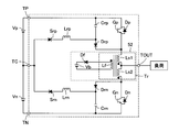
- FIG. 1 is a diagram showing a configuration of a soft switching inverter according to a first embodiment of the present invention.
- soft switching inverter (power converter) 101 includes DC power supplies Vp, Vn, power supply terminals TP, TC, TN, AC output terminal TOUT, main switches Gp, Gn, and main diode Dp. , Dn, snubber capacitors Crp, Crn, snubber diodes Drp, Drn, auxiliary switches Srp, Srn, auxiliary reactors Lrp, Lrn, and a protection circuit 51.
- Protection circuit 51 includes a transformer Tr and a clamp diode Df.
- the transformer Tr includes primary windings Ls1, Ls2 and a secondary winding Lf.
- the soft switching inverter 101 may be configured to include DC power supplies Vp and Vn.
- the main switches Gp and Gn are, for example, IGBTs (Insulated Gate Bipolar Transistors).
- the auxiliary switches Srp and Srn are, for example, reverse blocking thyristors.
- DC power supplies Vp and Vn are connected in series. That is, the DC power supply Vp has a positive electrode connected to the power supply terminal TP and a negative electrode connected to the power supply terminal TC.
- DC power supply Vn has a negative electrode of DC power supply Vp, a positive electrode connected to power supply terminal TC, and a negative electrode connected to power supply terminal TN.
- the main switch Gp has a collector coupled to the positive electrode of the DC power supply Vp and an emitter coupled to the load via the AC output terminal TOUT. That is, the main switch Gp has a collector connected to the power supply terminal TP and an emitter connected to the first end of the primary winding Ls1 of the transformer Tr.
- the main diode Dp is connected in parallel with the main switch Gp so that the conduction direction is opposite to that of the main switch Gp. That is, the main diode Dp has a cathode connected to the collector of the main switch Gp and an anode connected to the emitter of the main switch Gp.
- the snubber capacitor Crp is connected in parallel with the main switch Gp and the main diode Dp.
- the snubber diode Drp is connected in parallel with the main switch Gp and the main diode Dp so as to have the same conduction direction as the main switch Gp, and is connected in series with the snubber capacitor Crp. That is, snubber diode Drp has an anode connected to the second end of snubber capacitor Crp and the second end of auxiliary reactor Lrp, and a cathode connected to the emitter of main switch Gp and the anode of main diode Dp.
- Auxiliary switch Srp and auxiliary reactor Lrp are connected between a connection node of DC power supply Vp and DC power supply Vn, that is, between a power supply terminal TC and a connection node of snubber capacitor Crp and snubber diode Drp, and are connected in series with each other. That is, auxiliary switch Srp has an anode connected to power supply terminal TC and a cathode connected to the first end of auxiliary reactor Lrp.
- Auxiliary reactor Lrp has a first end connected to the cathode of auxiliary switch Srp and a second end connected to a connection node of snubber capacitor Crp and snubber diode Drp.
- the main switch Gn has a collector coupled to the emitter of the main switch Gp and an emitter coupled to the negative electrode of the DC power supply Vn, and is provided so as to have the same conduction direction as the main switch Gp. That is, the main switch Gn has a collector connected to the second end of the primary winding Ls2 of the transformer Tr and an emitter connected to the power supply terminal TN.
- the main diode Dn is connected in parallel with the main switch Gn so that the conduction direction is opposite to that of the main switch Gn. That is, the main diode Dn has a cathode connected to the collector of the main switch Gn and an anode connected to the emitter of the main switch Gn.
- the snubber capacitor Crn is connected in parallel with the main switch Gn and the main diode Dn.
- the snubber diode Drn is connected in parallel with the main switch Gn and the main diode Dn so as to have the same conduction direction as the main switch Gn, and is connected in series with the snubber capacitor Crn.
- snubber diode Drn has a cathode connected to the first end of snubber capacitor Crn and the second end of auxiliary reactor Lrn, and an anode connected to the collector of main switch Gn and the cathode of main diode Dn.
- Auxiliary switch Srn and auxiliary reactor Lrn are connected between DC power supply Vp and a connection node between DC power supply Vn and auxiliary switch Srp, that is, between power supply terminal TC and a connection node of snubber capacitor Crn and snubber diode Drn, and connected in series with each other.
- auxiliary switch Srn has a cathode connected to power supply terminal TC and an anode connected to the first end of auxiliary reactor Lrn.
- Auxiliary reactor Lrn has a first end connected to the anode of auxiliary switch Srn and a second end connected to a connection node of snubber capacitor Crn and snubber diode Drn.
- the protection circuit 51 is connected between the emitter of the main switch Gp and the collector of the main switch Gn.
- the primary windings Ls1 and Ls2 are connected between the emitter of the main switch Gp and the collector of the main switch Gn. That is, the primary winding Ls1 has a first end connected to the emitter of the main switch Gp and the cathode of the snubber diode Drp, and a second end connected to the AC output terminal TOUT and the first end of the primary winding Ls2. And have.
- the primary winding Ls2 has a first end connected to the AC output terminal TOUT and the second end of the primary winding Ls1, and a second end connected to the collector of the main switch Gn and the anode of the snubber diode Drn. Have.
- the primary windings Ls1 and Ls2 have the same winding direction.
- the secondary winding Lf is connected between the positive electrode of the DC power supply Vp and the negative electrode of the DC power supply Vn, and is magnetically coupled to the primary windings Ls1 and Ls2. That is, the secondary winding Lf has a first end connected to the anode of the clamp diode Df and a second end connected to the power supply terminal TN.
- the secondary winding Lf has a winding direction opposite to that of the primary windings Ls1 and Ls2. Further, the turns ratio of the primary winding and the secondary winding of the transformer Tr is 1: n, for example, n> 2.
- the clamp diode Df is connected between the positive electrode of the DC power supply Vp and the negative electrode of the DC power supply Vn, and is connected in series with the secondary winding Lf. That is, the clamp diode Df has a cathode connected to the power supply terminal TP and an anode connected to the first end of the secondary winding Lf.
- the soft switching inverter 101 switches the DC power supplied from the DC power supplies Vp and Vn by the main switches Gp and Gn which are main arms, thereby converting the DC power supplied from the DC power supply Vp and the DC power supply Vn into AC power.
- the voltage is converted and supplied to the load via the AC output terminal TOUT.
- the snubber capacitor Crp is provided to prevent voltage from being applied to the main switch Gp when the main switch Gp is turned off.
- the snubber capacitor Crn is provided to prevent a voltage from being applied to the main switch Gn when the main switch Gn is turned off.
- An anode reactor Lbp of the soft switching inverter shown in FIG. 2 is provided to prevent current from flowing through the main switch Gp when the main switch Gp is turned on.
- the anode reactor Lbn is provided to prevent current from flowing through the main switch Gn when the main switch Gn is turned on.
- the anode reactors Lbp and Lbn are not provided, but the primary windings Ls1 and Ls2 of the transformer Tr also serve as the anode reactors Lbp and Lbn.
- the protection circuit 51 has a current path PT between the positive electrode of the DC power supply Vp and the negative electrode of the DC power supply Vn.
- the protection circuit 51 suppresses the maximum voltage applied to the main switches Gp and Gn to the maximum value VM smaller than twice the output voltage of the DC power sources Vp and Vn.
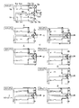
- FIG. 2 is a diagram showing a current flow in time series when the soft switching inverter according to the first embodiment of the present invention performs power conversion.
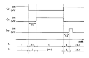
- FIG. 3 is a diagram showing a switch control procedure when the soft switching inverter according to the first embodiment of the present invention performs power conversion.
- the output voltage of the DC power supply Vp is Vp
- the output voltage of the DC power supply Vn is Vn.
- the horizontal axis of FIG. 3 indicates time, and the numbers in the upper stage A arranged along the horizontal axis indicate the transition of each step shown in FIG. 2 when the load current is somewhat large. That is, when the load current is large to some extent, the state of the soft switching inverter changes in the order of steps 1, 2, 4, 5, 6, 7, 8, and 1.
- main switch Gp is on-controlled
- main switch Gn is off-controlled
- auxiliary switches Srp and Srn are off-controlled, and from DC power supply Vp to load through main switch Gp.
- the description starts from a state where a current is flowing (step 1).
- the main switch Gp is turned off. Then, the current from the DC power supply Vp is commutated to the snubber capacitor Crp. As a result, the snubber capacitor Crp is charged, and the main diode Dn conducts when the voltage at the snubber capacitor Crp becomes equal to the output voltages (Vp + Vn) of the DC power supplies Vp and Vn (step 2).
- the main diode Dn becomes conductive, the current from the DC power source Vn flows to the load through the main diode Dn. Further, the resonance between the snubber capacitor Crp and the exciting inductance in the primary windings Ls1 and Ls2 reduces the current flowing from the snubber capacitor Crp to the snubber diode Drp, and eventually becomes zero. Then, the snubber diode Drp is turned off, and commutation from the DC power source Vp is completed (step 4).
- the main switch Gn is turned on when a predetermined time Tb has elapsed.
- the main switch Gn does not conduct and the current continues to flow to the load through the main diode Dn (step 5). That is, when the main switch Gn is on-controlled, no current flows through the main switch Gn. Thereby, zero current switching is realized.
- the main switch Gn is turned off, and immediately thereafter, the main switch Gp is turned on. Then, commutation from the main diode Dn to the main switch Gp starts. Then, the current flowing from the DC power source Vp through the main switch Gp increases and becomes equal to the load current. At the same time, the current flowing through the main diode Dn becomes zero and the main diode Dn is turned off, and this commutation is completed. Then, a current flows to the load through the main switch Gp (step 6).
- the auxiliary switch Srp is turned on when a predetermined time Td elapses after the main switch Gn is turned off.
- the snubber capacitor Crp begins to discharge.
- the snubber diode Drp conducts (step 7).
- Step 8 when the snubber diode Drp is turned on, a voltage from the DC power source Vp is applied to the auxiliary reactor Lrp. For this reason, the current flowing through the auxiliary switch Srp attenuates, and when it becomes zero, both the auxiliary switch Srp and the snubber diode Drp are turned off and the state returns to the state of Step 1 (Step 8).
- Each number in the lower stage B arranged along the horizontal axis in FIG. 3 indicates the transition of each step shown in FIG. 2 when the load current is very small. That is, when the load current is very small, the state of the soft switching inverter changes in the order of steps 1, 2, 3, 4, 5, 6, 7, 8, and 1.
- the soft switching inverter 101 controls the main switch Gn to turn on when a predetermined time Tb has elapsed since the main switch Gp is turned off. If the load current is very small, the charging of the snubber capacitor Crp in step 2 described above is not performed. Since it becomes extremely slow, the main switch Gn is turned on while the snubber capacitor Crp is charged in Step 2. If it does so, it will transfer to the state of step 3. Here, an increase in current flowing through the main switch Gn when the main switch Gn is turned on is suppressed by the excitation inductance in the primary windings Ls1 and Ls2 of the transformer Tr. Thereby, zero current switching is realized.
- step 3 the snubber capacitor Crp is charged by the resonance current between the snubber capacitor Crp and the exciting inductance in the primary windings Ls1 and Ls2 of the transformer Tr.
- the voltage difference between the output voltages (Vp + Vn) of the DC power sources Vp and Vn and the voltage Vc at the snubber capacitor Crp is applied to the series circuit of the primary windings Ls1 and Ls2 of the transformer Tr.
- the primary windings Ls1 and Ls2 each share a voltage that is 1 ⁇ 2 of the difference voltage. That is, the value VL of the voltage applied to the primary windings Ls1 and Ls2 is expressed by the following equation.
- VL ⁇ (Vp + Vn) -Vc ⁇ / 2 Since the turns ratio of the transformer Tr is 1: n, a voltage of n ⁇ VL is induced on the secondary side.
- Vp + Vn the voltage of the transformer Tr reaches the output voltage (Vp + Vn)
- the clamp diode Df is turned on and the snubber diode Drp is turned off.
- the maximum value VM of the voltage Vc at this time is expressed by the following equation.
- VM (1 + 2 / n) ⁇ (Vp + Vn)
- a current flows as indicated by a broken line shown in Step 3 of FIG. 2, the current flowing to the snubber capacitor Crp becomes zero, and the snubber capacitor Crp is not charged.
- the voltage Vc at the snubber capacitor Crp is clamped to VM.
- the current flowing through the main switch Gn decreases, and when it becomes zero, the main switch Gn is turned off, the main diode Dn is turned on, and the state of Step 4 described above is entered.
- the main switch Gn is already on-controlled, the main switch Gn is not on-controlled in step 5.
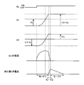
- FIG. 4 is a diagram showing the current flow in steps 3 and 4 of the soft switching inverter according to the first embodiment of the present invention in time series.
- FIG. 5 is a waveform diagram of voltages and currents in steps 3 and 4 of the soft switching inverter according to the first embodiment of the present invention.
- FIG. 4 shows an equivalent circuit of the soft switching inverter 101 in steps 3 and 4.
- the circuit that does not conduct in steps 3 and 4 is omitted, and in order to facilitate understanding of the operation, the portion of the transformer Tr is divided into an ideal transformer and an exciting inductance that exists in parallel with each winding. It shows in detail.
- Lsid1 and Lsid2 are primary windings of the ideal transformer, and Lfid is the secondary winding of the ideal transformer.
- L1 is the excitation inductance on the primary side of the transformer Tr
- L2 is the excitation inductance on the secondary side of the transformer Tr.
- Vc is the voltage at the snubber capacitor Crp
- V1 is the voltage at the primary winding of the transformer Tr
- V2 is the voltage at the secondary winding of the transformer Tr.
- the direction of each arrow is positive.
- step 3 a case where the load current is zero will be described for easy understanding.
- the snubber capacitor Crp is not charged at all in step 2 described above, and the process proceeds to step 3 as it is.
- step 3 will be described by dividing it into three modes 1 to 3 in time series. That is, mode 1 is a state at the start of step 3, mode 2 is a state after clamp diode Df is turned on, and mode 3 is a state after snubber diode Drp is turned off.
- the clamp diode Df becomes conductive.
- a current I2 flows through the secondary winding Lfid of the ideal transformer, and a current I1 that is twice the current I2 flows through the primary windings Lsid1 and Lsid2 of the ideal transformer due to the transformer action.
- the current I1 acts to cancel the charging current of the snubber capacitor Crp, that is, the current I3.
- the current I3 flowing through the snubber capacitor Crp and the snubber diode Drp becomes zero, and the snubber diode Drp is turned off.
- the voltage Vc does not increase, so that the voltage Vc is maintained at 1.5 ⁇ Vs (mode 2).
- the voltage Vc at the snubber capacitor Crp is the voltage.
- the value VM energy to flow current through the primary windings Ls1 and Ls2 of the transformer Tr is transferred to the secondary winding Lf of the transformer Tr, and the charging current does not flow through the snubber capacitor Crp. For this reason, the charging of the snubber capacitor Crp stops, and the maximum voltage of the snubber capacitor Crp is clamped to VM.
- VM becomes equal to or less than twice Vs. Further, if n is increased, VM ⁇ (Vp + Vn). Therefore, the voltage Vc at the snubber capacitor Crp can be suppressed to a value as close as possible to the power supply voltage Vs.
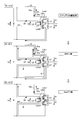
- FIG. 6 is a diagram showing current flow in time series when the soft switching inverter according to the first embodiment of the present invention performs power conversion.
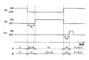
- FIG. 7 is a diagram showing a switch control procedure when the soft switching inverter according to the first embodiment of the present invention performs power conversion.
- the output voltage of the DC power supply Vn is Vn
- the output voltage of the DC power supply Vp is Vp.
- the horizontal axis in FIG. 7 indicates time, and the numbers in the upper stage A arranged along the horizontal axis indicate the transition of each step shown in FIG. 6 when the load current is somewhat large. That is, when the load current is large to some extent, the state of the soft switching inverter transitions in the order of steps 11, 12, 14, 15, 16, 17, 18, 11.
- main switch Gn is on-controlled
- main switch Gp is off-controlled
- auxiliary switches Srn and Srp are off-controlled from load to DC power source Vn through main switch Gn.
- the description starts from the state in which current is flowing (step 11).
- the main switch Gn is turned off. Then, the current from the load is commutated to the snubber capacitor Crn. As a result, the snubber capacitor Crn is charged, and the main diode Dp conducts when the voltage at the snubber capacitor Crn becomes equal to the output voltages (Vn + Vp) of the DC power supplies Vn and Vp (step 12).
- step 12 when the main switch Gn is turned off, a current flows to the snubber capacitor Crn.
- the main switch Gn When the main switch Gn is turned off, no charge is applied to the main switch Gn because the electric charge of the snubber capacitor Crn is zero. Thereby, zero volt switching is realized.
- the main diode Dp when the main diode Dp is turned on, the current from the load flows to the DC power source Vp through the main diode Dp. Further, the resonance between the snubber capacitor Crn and the exciting inductance in the primary windings Ls1 and Ls2 reduces the current flowing from the snubber diode Drn to the snubber capacitor Crn and eventually becomes zero. Then, the snubber diode Drn is turned off and commutation from the load is completed (step 14).
- the main switch Gp is turned on when a predetermined time Tb has elapsed.
- the main switch Gp since the current from the load to the main diode Dp has a current polarity opposite to that of the main switch Gp, the main switch Gp does not conduct, and the current continues to flow to the DC power source Vp through the main diode Dp (step 15). That is, when the main switch Gp is on-controlled, no current flows through the main switch Gp. Thereby, zero current switching is realized.
- the main switch Gp is turned off, and immediately thereafter, the main switch Gn is turned on. Then, commutation from the main diode Dp to the main switch Gn starts. Then, the current flowing from the DC power source Vn through the main switch Gn increases and becomes equal to the load current. At the same time, the current flowing through the main diode Dp becomes zero, and the main diode Dp is turned off, and this commutation is completed. Then, a current flows to the DC power source Vn through the main switch Gn (step 16).
- the auxiliary switch Srn is turned on when a predetermined time Td has elapsed. Thereby, discharge of the snubber capacitor Crn starts. When this discharge is completed and the voltage at the snubber capacitor Crn becomes zero, the snubber diode Drn becomes conductive (step 17).
- step 18 when the snubber diode Drn becomes conductive, the voltage from the DC power source Vn is applied to the auxiliary reactor Lrn. For this reason, the current flowing through the auxiliary switch Srn is attenuated, and when it becomes zero, both the auxiliary switch Srn and the snubber diode Drn are turned off and the state returns to the state of step 11 (step 18).
- Each number in the lower stage B arranged along the horizontal axis in FIG. 7 indicates the transition of each step shown in FIG. 6 when the load current is very small. That is, when the load current is very small, the state of the soft switching inverter transitions in the order of steps 11, 12, 13, 14, 15, 16, 17, 18, 11.
- the main switch Gp is turned on when the predetermined time Tb elapses after the main switch Gn is turned off. If the load current is very small, the charging of the snubber capacitor Crn in the above-described step 12 is not performed. Since it becomes extremely slow, the main switch Gp is turned on while the snubber capacitor Crn is charged in step 12. If it does so, it will transfer to the state of step 13.
- an increase in the current flowing through the main switch Gp when the main switch Gp is on-controlled is suppressed by the excitation inductance in the primary windings Ls1 and Ls2 of the transformer Tr. Thereby, zero current switching is realized.
- step 13 the snubber capacitor Crn is charged by the resonance current between the snubber capacitor Crn and the exciting inductance in the primary windings Ls1 and Ls2 of the transformer Tr.
- the difference voltage between the output voltage (Vn + Vp) of the DC power sources Vn and Vp and the voltage Vc at the snubber capacitor Crn is applied to the series circuit of the primary windings Ls1 and Ls2 of the transformer Tr.
- the primary windings Ls1 and Ls2 each share a voltage that is 1 ⁇ 2 of the difference voltage. That is, the value VL of the voltage applied to the primary windings Ls1 and Ls2 is expressed by the following equation.
- VL ⁇ (Vn + Vp) ⁇ Vc ⁇ / 2 Since the turns ratio of the transformer Tr is 1: n, a voltage of n ⁇ VL is induced on the secondary side.
- Vn + Vp the voltage of the transformer Tr
- the clamp diode Df is turned on and the snubber diode Drn is turned off.
- the maximum value VM of the voltage Vc at this time is expressed by the following equation.
- VM (1 + 2 / n) ⁇ (Vn + Vp)
- a current flows as indicated by a broken line shown in step 13 of FIG. 6, the current flowing to the snubber capacitor Crn becomes zero, and the snubber capacitor Crn is not charged.
- the voltage Vc at the snubber capacitor Crn is clamped to VM.
- the current flowing through the main switch Gp decreases, and when it becomes zero, the main switch Gp is turned off, the main diode Dp is turned on, and the process proceeds to the state of step 14 described above.
- the main switch Gp is already on-controlled, the main switch Gp is not on-controlled in step 15.
- FIG. 8 is a diagram showing the current flow in steps 13 and 14 of the soft switching inverter according to the first embodiment of the present invention in time series.
- FIG. 9 is a waveform diagram of voltages and currents in steps 13 and 14 of the soft switching inverter according to the first embodiment of the present invention.
- FIG. 8 shows an equivalent circuit of the soft switching inverter 101 in steps 13 and 14.
- this equivalent circuit a circuit that does not conduct in steps 13 and 14 is omitted, and in order to facilitate understanding of the operation, the portion of the transformer Tr is divided into an ideal transformer and an exciting inductance that exists in parallel with each winding. It shows in detail.
- Lsid1 and Lsid2 are primary windings of the ideal transformer, and Lfid is the secondary winding of the ideal transformer.
- L1 is the excitation inductance on the primary side of the transformer Tr
- L2 is the excitation inductance on the secondary side of the transformer Tr.
- Vc is the voltage at the snubber capacitor Crn
- V1 is the voltage at the primary winding of the transformer Tr
- V2 is the voltage at the secondary winding of the transformer Tr.
- the direction of each arrow is positive.
- step 12 the snubber capacitor Crn is not charged at all in step 12 described above, and the process proceeds to step 13 as it is.
- step 13 will be described by dividing it into three modes 1 to 3 in time series. That is, mode 1 is a state at the start of step 13, mode 2 is a state after the clamp diode Df is turned on, and mode 3 is a state after the snubber diode Drn is turned off.
- the clamp diode Df becomes conductive.
- a current I2 flows through the secondary winding Lfid of the ideal transformer, and a current I1 that is twice the current I2 flows through the primary windings Lsid1 and Lsid2 of the ideal transformer due to the transformer action.
- the current I1 acts to cancel the charging current of the snubber capacitor Crn, that is, the current I3.
- the current I3 flowing through the snubber capacitor Crn and the snubber diode Drn becomes zero, and the snubber diode Drn is turned off.
- the voltage Vc does not increase, so that the voltage Vc is maintained at 1.5 ⁇ Vs (mode 2).
- the voltage Vc at the snubber capacitor Crn is the voltage.
- the value VM the energy to flow current through the primary windings Ls1 and Ls2 of the transformer Tr is transferred to the secondary winding Lf of the transformer Tr, and the charging current does not flow through the snubber capacitor Crn. For this reason, the charging of the snubber capacitor Crn stops, and the maximum voltage of the snubber capacitor Crn is clamped to VM.
- VM becomes equal to or less than twice Vs. Further, if n is increased, VM ⁇ (Vn + Vp), so that the voltage Vc at the snubber capacitor Crn can be suppressed to a value as close as possible to the power supply voltage Vs.
- the soft switching inverter 101 repeats the operations of Steps 1 to 8 shown in FIG. 2 as the operation in the positive period, and repeats the operations of Steps 11 to 18 shown in FIG. 6 as the operation in the negative period.
- Soft switching inverter 101 supplies alternating current power to the load by alternately performing such positive period operation and negative period operation.
- Non-Patent Document 1 when the load is light, the snubber capacitor is charged up to twice the power supply voltage, and a high voltage is applied to the main switch and the main diode. For this reason, these devices are required to have a withstand voltage that is twice or more the power supply voltage, which increases the size of the soft switching inverter and increases the cost.
- the protection circuit 51 supplies the snubber capacitor Crp with a charging current that tends to flow from the DC power source Vp and the DC power source Vn to the snubber capacitor Crp or the snubber capacitor Crn.
- the voltage applied to the capacitor exceeds a predetermined value, or when the voltage applied to the snubber capacitor Crn exceeds the predetermined value, the positive electrode of the DC power source Vp and the negative electrode of the DC power source Vn via the current path PT Shed in between.
- the protection circuit 51 includes the voltage difference between the output voltage of the DC power supply Vp and the DC power supply Vn and the voltage applied to the snubber capacitor Crp, or the output voltage of the DC power supply Vp and the DC power supply Vn and the snubber capacitor.
- a voltage obtained by boosting the received voltage is generated.
- the positive electrode of the DC power supply Vp and the DC power supply Vn are connected via the current path PT. Switches whether or not a charging current flows between the negative electrodes.
- the maximum charging voltage of the snubber capacitor is set to the power supply voltage by inserting a transformer and setting the turns ratio to 1: n (n> 2). To within 2 times.
- the protection circuit 51 turns to the primary winding of the transformer when the voltage applied to the snubber capacitor reaches a predetermined voltage.
- the energy to pass current is transferred to the secondary winding of the transformer.
- the charging current stops flowing through the snubber capacitor and charging is stopped, and the voltage applied to the snubber capacitor is clamped.
- the clamp voltage becomes less than twice the power supply voltage, and if n is increased, the voltage applied to the snubber capacitor is suppressed to a value close to the power supply voltage. can do.
- the breakdown voltage of these elements can be lowered, so that the apparatus can be downsized and the cost can be reduced.
- an output voltage higher than that of the prior art can be obtained. That is, since the voltage utilization factor of the main switch and the main diode is improved by suppressing the charging voltage of the snubber capacitor, a higher output voltage can be obtained using elements having the same breakdown voltage.
- the protection circuit is not limited to the configuration shown in FIG. 1, and the voltage applied to the snubber capacitor Crp exceeds a predetermined value or the voltage applied to the snubber capacitor Crn exceeds a predetermined value.
- any configuration may be employed as long as the charging current that is about to flow from the DC power source Vp and the DC power source Vn to the snubber capacitor Crp or the snubber capacitor Crn is released to another current path.
- FIG. 10 is a diagram showing a configuration of a modified example of the soft switching inverter according to the first embodiment of the present invention.
- the soft switching inverter includes a protection circuit 52 instead of the protection circuit 51 as compared with the soft switching inverter 101.
- Protection circuit 52 includes a transformer Tr, a clamp diode Df, and a DC power supply Vb.
- DC power supply Vb has a positive electrode connected to the cathode of clamp diode Df and a negative electrode connected to the anode of clamp diode Df.
- the cathode of the clamp diode Df is connected to the positive electrode of the DC power supply Vp.
- the present invention is not limited to this. That is, as shown in FIG. 10, the protection circuit 52 may include a DC power supply Vb different from the DC power supplies Vp and Vn.
- the protection circuit 52 detects the snubber capacitor Crp from the DC power source Vp and the DC power source Vn. Alternatively, a charging current that is about to flow to the snubber capacitor Crn is passed to the DC power source Vb via the clamp diode Df.
- the voltage applied to the snubber capacitor can be applied to the DC power sources Vp and Vn without boosting the difference voltage between the output voltage of the DC power sources Vp and Vn and the voltage Vc of the snubber capacitor by the transformer Tr.
- the clamp diode Df can be turned on before the output voltage is doubled, for example, so that the voltage applied to the snubber capacitor can be limited to less than twice the output voltage of the DC power supplies Vp and Vn. .
- the present embodiment relates to a soft switching inverter provided with an alternative circuit for a transformer as compared with the soft switching inverter according to the first embodiment.
- the contents other than those described below are the same as those of the soft switching inverter according to the first embodiment.
- FIG. 11 is a diagram showing a configuration of the soft switching inverter according to the second embodiment of the present invention.
- the soft switching inverter 102 includes a protection circuit 53 instead of the protection circuit 51 as compared with the soft switching inverter according to the first embodiment of the present invention.
- Protection circuit 53 includes an anode reactor Lb, a clamp diode Df, and a DC power supply Vb.
- Anode reactor Lb has a first end connected to the emitter of main switch Gp and a second end connected to the collector of main switch Gn.
- the DC power supply Vb and the clamp diode Df are connected in series between both ends of the anode reactor Lb. That is, DC power supply Vb has a positive electrode connected to the cathode of clamp diode Df and a negative electrode connected to the first end of anode reactor Lb.
- the clamp diode Df has an anode connected to the second end of the anode reactor Lb.
- the protection circuit 53 When the voltage applied to the snubber capacitor Crp exceeds a predetermined value or when the voltage applied to the snubber capacitor Crn exceeds a predetermined value, the protection circuit 53 generates a snubber capacitor Crp from the DC power source Vp and the DC power source Vn. Alternatively, the charging current that is about to flow to the snubber capacitor Crn is released to the DC power source Vb via the clamp diode Df.
- the present embodiment relates to a soft switching inverter in which an anode reactor is added as compared with the soft switching inverter according to the first embodiment.
- the contents other than those described below are the same as those of the soft switching inverter according to the first embodiment.
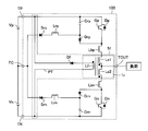
- FIG. 12 is a diagram showing a configuration of the soft switching inverter according to the third embodiment of the present invention.
- soft switching inverter 103 further includes anode reactors Lbp and Lbn as compared with the soft switching inverter according to the first embodiment of the present invention.
- Anode reactor Lbp has a first end connected to the cathode of snubber diode Drp, the emitter of main switch Gp, and the anode of main diode Dp, and a second end connected to the first end of primary winding Ls1.
- Anode reactor Lbn has a first end connected to the second end of primary winding Ls2, and a second end connected to the anode of snubber diode Drn, the collector of main switch Gn, and the cathode of main diode Dn.
- the present embodiment relates to a soft switching inverter in which an anode reactor is added as compared with the soft switching inverter according to the first embodiment.
- the contents other than those described below are the same as those of the soft switching inverter according to the first embodiment.
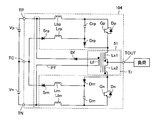
- FIG. 13 is a diagram showing the configuration of the soft switching inverter according to the fourth embodiment of the present invention.
- soft switching inverter 104 further includes anode reactors Lbp and Lbn as compared with the soft switching inverter according to the first embodiment of the present invention.
- the anode reactor Lbp has a first end connected to the power supply terminal TP and the cathode of the clamp diode Df, a first end of the snubber capacitor Crp, a collector of the main switch Gp, and a second end connected to the cathode of the main diode Dp.
- the anode reactor Lbn is connected to the first end connected to the power supply terminal TN and the second end of the secondary winding Lf, the second end of the snubber capacitor Crn, the emitter of the main switch Gn, and the anode of the main diode Dn. And a second end.
Landscapes
- Engineering & Computer Science (AREA)
- Power Engineering (AREA)
- Inverter Devices (AREA)
- Dc-Dc Converters (AREA)
Abstract
Description
図1は、本発明の第1の実施の形態に係るソフトスイッチングインバータの構成を示す図である。
図2は、本発明の第1の実施の形態に係るソフトスイッチングインバータが電力変換を行なう際の電流の流れを時系列的に示す図である。図3は、本発明の第1の実施の形態に係るソフトスイッチングインバータが電力変換を行なう際のスイッチ制御手順を示す図である。ここでは、直流電源Vpの出力電圧をVpとし、直流電源Vnの出力電圧をVnとする。
変圧器Trの巻数比は1:nであるので、2次側にはn×VLの電圧が誘起される。スナバコンデンサCrpにおける電圧Vcが上昇し、変圧器Trの2次側電圧が出力電圧(Vp+Vn)に達すると、クランプダイオードDfがオンしてスナバダイオードDrpがオフする。このときの電圧Vcの最大値VMは、以下の式で表わされる。
そして、図2のステップ3に示す破線のように電流が流れ、スナバコンデンサCrpへ流れる電流はゼロとなり、スナバコンデンサCrpは充電されなくなる。これにより、スナバコンデンサCrpにおける電圧VcはVMにクランプされる。その後、主スイッチGnを通して流れる電流が減少し、ゼロになると主スイッチGnがオフし、主ダイオードDnが導通して、前述のステップ4の状態に移行する。但し、主スイッチGnはすでにオン制御されているので、ステップ5において主スイッチGnのオン制御は行なわれない。
図6は、本発明の第1の実施の形態に係るソフトスイッチングインバータが電力変換を行なう際の電流の流れを時系列的に示す図である。図7は、本発明の第1の実施の形態に係るソフトスイッチングインバータが電力変換を行なう際のスイッチ制御手順を示す図である。ここでは、直流電源Vnの出力電圧をVnとし、直流電源Vpの出力電圧をVpとする。
変圧器Trの巻数比は1:nであるので、2次側にはn×VLの電圧が誘起される。スナバコンデンサCrnにおける電圧Vcが上昇し、変圧器Trの2次側電圧が出力電圧(Vn+Vp)に達すると、クランプダイオードDfがオンしてスナバダイオードDrnがオフする。このときの電圧Vcの最大値VMは、以下の式で表わされる。
そして、図6のステップ13に示す破線のように電流が流れ、スナバコンデンサCrnへ流れる電流はゼロとなり、スナバコンデンサCrnは充電されなくなる。これにより、スナバコンデンサCrnにおける電圧VcはVMにクランプされる。その後、主スイッチGpを通して流れる電流が減少し、ゼロになると主スイッチGpがオフし、主ダイオードDpが導通して、前述のステップ14の状態に移行する。但し、主スイッチGpはすでにオン制御されているので、ステップ15において主スイッチGpのオン制御は行なわれない。
本実施の形態は、第1の実施の形態に係るソフトスイッチングインバータと比べてトランスの代替回路を備えたソフトスイッチングインバータに関する。以下で説明する内容以外は第1の実施の形態に係るソフトスイッチングインバータと同様である。
本実施の形態は、第1の実施の形態に係るソフトスイッチングインバータと比べてアノードリアクトルを追加したソフトスイッチングインバータに関する。以下で説明する内容以外は第1の実施の形態に係るソフトスイッチングインバータと同様である。
本実施の形態は、第1の実施の形態に係るソフトスイッチングインバータと比べてアノードリアクトルを追加したソフトスイッチングインバータに関する。以下で説明する内容以外は第1の実施の形態に係るソフトスイッチングインバータと同様である。
Claims (6)
- 第1電極および第2電極を有する第1の直流電源(Vp)と、前記第1の直流電源(Vp)の第2電極に接続される第1電極、および第2電極を有する第2の直流電源(Vn)とから供給された直流電力を交流電力に変換して負荷に供給する電力変換装置であって、
前記第1の直流電源(Vp)の第1電極に結合される第1端と、前記負荷に結合される第2端とを有する第1の主スイッチ(Gp)と、
前記第1の主スイッチ(Gp)と導通方向が逆になるように、前記第1の主スイッチ(Gp)と並列接続される第1の主ダイオード(Dp)と、
前記第1の主スイッチ(Gp)および前記第1の主ダイオード(Dp)と並列接続される第1のスナバコンデンサ(Crp)と、
前記第1の主スイッチ(Gp)と導通方向が同じになるように、前記第1のスナバコンデンサ(Crp)と直列接続され、かつ前記第1のスナバコンデンサ(Crp)と前記第1の主スイッチ(Gp)の第2端との間に接続される第1のスナバダイオード(Drp)と、
前記第1の直流電源(Vp)および前記第2の直流電源(Vn)の接続ノードと前記第1のスナバコンデンサ(Crp)および前記第1のスナバダイオード(Drp)の接続ノードとの間に接続され、かつ互いに直列接続される第1の補助スイッチ(Srp)および第1の補助リアクトル(Lrp)と、
前記第1の主スイッチ(Gp)の第2端に結合される第1端と、前記第2の直流電源(Vn)の第2電極に結合される第2端とを有し、前記第1の主スイッチ(Gp)と導通方向が同じになるように設けられる第2の主スイッチ(Gn)と、
前記第2の主スイッチ(Gn)と導通方向が逆になるように、前記第2の主スイッチ(Gn)と並列接続される第2の主ダイオード(Dn)と、
前記第2の主スイッチ(Gn)および前記第2の主ダイオード(Dn)と並列接続される第2のスナバコンデンサ(Crn)と、
前記第2の主スイッチ(Gn)と導通方向が同じになるように、前記第2のスナバコンデンサ(Crn)と直列接続され、かつ前記第2のスナバコンデンサ(Crn)と前記第2の主スイッチ(Gn)の第1端との間に接続される第2のスナバダイオード(Drn)と、
前記第1の直流電源(Vp)および前記第2の直流電源(Vn)と前記第1の補助スイッチ(Srp)または前記第1の補助リアクトル(Lrp)との接続ノードと前記第2のスナバコンデンサ(Crn)および前記第2のスナバダイオード(Drn)の接続ノードとの間に接続され、かつ互いに直列接続される第2の補助スイッチ(Srn)および第2の補助リアクトル(Lrn)と、
前記第1のスナバコンデンサ(Crp)に印加される電圧が所定値以上になった場合または前記第2のスナバコンデンサ(Crn)に印加される電圧が所定値以上になった場合、前記第1の直流電源(Vp)および前記第2の直流電源(Vn)から前記第1のスナバコンデンサ(Crp)または前記第2のスナバコンデンサ(Crn)へ流れようとする充電電流を他の電流経路へ流すための保護回路(51,52,53)とを備える電力変換装置。 - 前記保護回路(51)は、前記第1の直流電源(Vp)の第1電極と前記第2の直流電源(Vn)の第2電極との間の電流経路を有し、前記第1のスナバコンデンサ(Crp)に印加される電圧が所定値以上になった場合または前記第2のスナバコンデンサ(Crn)に印加される電圧が所定値以上になった場合、前記電流経路を介して前記第1の直流電源(Vp)の第1電極および前記第2の直流電源(Vn)の第2電極間に前記充電電流を流す請求の範囲第1項に記載の電力変換装置。
- 前記保護回路(51)は、前記第1の直流電源(Vp)および前記第2の直流電源(Vn)の出力電圧と前記第1のスナバコンデンサ(Crp)に印加される電圧との差の電圧、または前記第1の直流電源(Vp)および前記第2の直流電源(Vn)の出力電圧と前記第2のスナバコンデンサ(Crn)に印加される電圧との差の電圧を受けて、受けた前記電圧を昇圧した電圧を生成し、生成した前記電圧に基づいて、前記電流経路を介して前記第1の直流電源(Vp)の第1電極および前記第2の直流電源(Vn)の第2電極間に前記充電電流を流すか否かを切り替える請求の範囲第2項に記載の電力変換装置。
- 前記保護回路(51)は、前記第1の主スイッチ(Gp)の第2端と前記第2の主スイッチ(Gn)の第1端との間に接続される請求の範囲第3項に記載の電力変換装置。
- 前記保護回路(51,52)は、前記第1の直流電源(Vp)および前記第2の直流電源(Vn)の出力電圧と前記第1のスナバコンデンサ(Crp)に印加される電圧との差の電圧、または前記第1の直流電源(Vp)および前記第2の直流電源(Vn)の出力電圧と前記第2のスナバコンデンサ(Crn)に印加される電圧との差の電圧を受けて、受けた前記電圧を昇圧した電圧を生成し、生成した前記電圧に基づいて、前記充電電流を他の電流経路へ流すか否かを切り替える請求の範囲第1項に記載の電力変換装置。
- 前記保護回路(51)は、
前記第1の主スイッチ(Gp)の第2端と前記第2の主スイッチ(Gn)の第1端との間に接続される1次巻線と、
前記第1の直流電源(Vp)の第1電極と前記第2の直流電源(Vn)の第2電極との間に接続され、前記1次巻線と磁気結合される2次巻線と、
前記第1の直流電源(Vp)の第1電極と前記第2の直流電源(Vn)の第2電極との間に接続され、前記2次巻線と直列接続されるクランプダイオードとを含む請求の範囲第1項に記載の電力変換装置。
Priority Applications (3)
| Application Number | Priority Date | Filing Date | Title |
|---|---|---|---|
| US13/266,054 US8605470B2 (en) | 2009-04-27 | 2009-04-27 | Power converter performing soft switching |
| PCT/JP2009/058252 WO2010125630A1 (ja) | 2009-04-27 | 2009-04-27 | 電力変換装置 |
| JP2011511201A JP5284465B2 (ja) | 2009-04-27 | 2009-04-27 | 電力変換装置 |
Applications Claiming Priority (1)
| Application Number | Priority Date | Filing Date | Title |
|---|---|---|---|
| PCT/JP2009/058252 WO2010125630A1 (ja) | 2009-04-27 | 2009-04-27 | 電力変換装置 |
Publications (1)
| Publication Number | Publication Date |
|---|---|
| WO2010125630A1 true WO2010125630A1 (ja) | 2010-11-04 |
Family
ID=43031798
Family Applications (1)
| Application Number | Title | Priority Date | Filing Date |
|---|---|---|---|
| PCT/JP2009/058252 Ceased WO2010125630A1 (ja) | 2009-04-27 | 2009-04-27 | 電力変換装置 |
Country Status (3)
| Country | Link |
|---|---|
| US (1) | US8605470B2 (ja) |
| JP (1) | JP5284465B2 (ja) |
| WO (1) | WO2010125630A1 (ja) |
Cited By (2)
| Publication number | Priority date | Publication date | Assignee | Title |
|---|---|---|---|---|
| WO2013128631A1 (ja) * | 2012-03-02 | 2013-09-06 | 東芝三菱電機産業システム株式会社 | 電力変換装置 |
| WO2013128632A1 (ja) * | 2012-03-02 | 2013-09-06 | 東芝三菱電機産業システム株式会社 | 電力変換装置 |
Families Citing this family (3)
| Publication number | Priority date | Publication date | Assignee | Title |
|---|---|---|---|---|
| WO2011024247A1 (ja) | 2009-08-24 | 2011-03-03 | 東芝三菱電機産業システム株式会社 | 同期機起動装置 |
| US8508962B2 (en) * | 2009-09-24 | 2013-08-13 | Toshiba Mitsubishi-Electric Industrial Systems Corporation | Power conversion apparatus |
| WO2015094374A1 (en) * | 2013-12-20 | 2015-06-25 | Intel Corporation | Apparatus for charge recovery during low power mode |
Citations (3)
| Publication number | Priority date | Publication date | Assignee | Title |
|---|---|---|---|---|
| JPH0568380A (ja) * | 1991-04-26 | 1993-03-19 | Mitsubishi Electric Corp | インバータ装置 |
| JP2001054279A (ja) * | 1999-05-28 | 2001-02-23 | Mitsubishi Electric Corp | スナバ回路 |
| JP2002199737A (ja) * | 2000-12-28 | 2002-07-12 | Fuji Electric Co Ltd | 電力変換装置 |
Family Cites Families (13)
| Publication number | Priority date | Publication date | Assignee | Title |
|---|---|---|---|---|
| US4276588A (en) * | 1979-06-22 | 1981-06-30 | Mclyman W T | Push-pull converter with energy saving circuit for protecting switching transistors from peak power stress |
| US5198969A (en) * | 1990-07-13 | 1993-03-30 | Design Automation, Inc. | Soft-switching full-bridge dc/dc converting |
| US5047913A (en) | 1990-09-17 | 1991-09-10 | General Electric Company | Method for controlling a power converter using an auxiliary resonant commutation circuit |
| US5513088A (en) * | 1991-06-14 | 1996-04-30 | Williamson; Floyd | Uninterruptable off-line, isolated flyback topology switch-mode power supply |
| WO2001084699A1 (en) * | 2000-04-28 | 2001-11-08 | Tdk Corporation | Power converting device |
| US6366474B1 (en) * | 2000-09-29 | 2002-04-02 | Jeff Gucyski | Switching power supplies incorporating power factor correction and/or switching at resonant transition |
| JP2004242491A (ja) * | 2002-11-29 | 2004-08-26 | Sony Corp | スイッチング電源回路 |
| US7706161B2 (en) * | 2006-03-14 | 2010-04-27 | Energy Conservation Technologies, Inc. | Single stage resonant power converter with auxiliary power source |
| JP4406733B2 (ja) * | 2006-10-05 | 2010-02-03 | 国立大学法人東京工業大学 | インバータ電源装置 |
| JP4824524B2 (ja) * | 2006-10-25 | 2011-11-30 | 日立アプライアンス株式会社 | 単方向dc−dcコンバータおよびその制御方法 |
| TWI358188B (en) * | 2008-09-17 | 2012-02-11 | Delta Electronics Inc | Forward-flyback converter with active-clamp circui |
| JP4988925B2 (ja) * | 2009-02-06 | 2012-08-01 | 株式会社三社電機製作所 | インバータ回路 |
| US8508962B2 (en) * | 2009-09-24 | 2013-08-13 | Toshiba Mitsubishi-Electric Industrial Systems Corporation | Power conversion apparatus |
-
2009
- 2009-04-27 US US13/266,054 patent/US8605470B2/en not_active Expired - Fee Related
- 2009-04-27 JP JP2011511201A patent/JP5284465B2/ja not_active Expired - Fee Related
- 2009-04-27 WO PCT/JP2009/058252 patent/WO2010125630A1/ja not_active Ceased
Patent Citations (3)
| Publication number | Priority date | Publication date | Assignee | Title |
|---|---|---|---|---|
| JPH0568380A (ja) * | 1991-04-26 | 1993-03-19 | Mitsubishi Electric Corp | インバータ装置 |
| JP2001054279A (ja) * | 1999-05-28 | 2001-02-23 | Mitsubishi Electric Corp | スナバ回路 |
| JP2002199737A (ja) * | 2000-12-28 | 2002-07-12 | Fuji Electric Co Ltd | 電力変換装置 |
Cited By (10)
| Publication number | Priority date | Publication date | Assignee | Title |
|---|---|---|---|---|
| WO2013128631A1 (ja) * | 2012-03-02 | 2013-09-06 | 東芝三菱電機産業システム株式会社 | 電力変換装置 |
| WO2013128632A1 (ja) * | 2012-03-02 | 2013-09-06 | 東芝三菱電機産業システム株式会社 | 電力変換装置 |
| CN104145413A (zh) * | 2012-03-02 | 2014-11-12 | 东芝三菱电机产业系统株式会社 | 功率转换装置 |
| CN104160609A (zh) * | 2012-03-02 | 2014-11-19 | 东芝三菱电机产业系统株式会社 | 功率转换装置 |
| JPWO2013128631A1 (ja) * | 2012-03-02 | 2015-07-30 | 東芝三菱電機産業システム株式会社 | 電力変換装置 |
| EP2822170A4 (en) * | 2012-03-02 | 2016-01-06 | Toshiba Mitsubishi Elec Inc | POWER CONVERTER |
| US9281740B2 (en) | 2012-03-02 | 2016-03-08 | Toshiba Mitsubishi-Electric Industrial Systems Corporation | Power conversion apparatus |
| CN104160609B (zh) * | 2012-03-02 | 2016-12-28 | 东芝三菱电机产业系统株式会社 | 功率转换装置 |
| US9621026B2 (en) | 2012-03-02 | 2017-04-11 | Toshiba Mitsubishi-Electric Industrial Systems Corporation | Power conversion apparatus |
| CN104145413B (zh) * | 2012-03-02 | 2017-07-14 | 东芝三菱电机产业系统株式会社 | 功率转换装置 |
Also Published As
| Publication number | Publication date |
|---|---|
| JPWO2010125630A1 (ja) | 2012-10-25 |
| US8605470B2 (en) | 2013-12-10 |
| JP5284465B2 (ja) | 2013-09-11 |
| US20120051103A1 (en) | 2012-03-01 |
Similar Documents
| Publication | Publication Date | Title |
|---|---|---|
| US11689115B2 (en) | Bidirectional AC-DC converter with multilevel power factor correction | |
| CN102959846B (zh) | Dc-dc变换器 | |
| CN107251398B (zh) | Dc-dc转换器 | |
| CN105144561B (zh) | Dc/dc转换器 | |
| US8508965B2 (en) | Inverter and method for operating the inverter | |
| US8508962B2 (en) | Power conversion apparatus | |
| US9787197B2 (en) | Switching power supply unit | |
| JP5284465B2 (ja) | 電力変換装置 | |
| US12246609B2 (en) | Charging device and method for operating the charging device | |
| JP6709965B2 (ja) | スナバ回路、及びそれを用いた電力変換システム | |
| US12512745B2 (en) | Power conversion device | |
| JP5749853B2 (ja) | 電力変換装置 | |
| JP5325991B2 (ja) | 電力変換装置 | |
| CN115411921A (zh) | 一种变换器和逆变器 | |
| CN222029832U (zh) | 逆变器和光伏发电系统 | |
| JP7160719B2 (ja) | ワンコンバータ方式の絶縁型スイッチング電源 | |
| JP7489039B2 (ja) | 電力変換装置の制御装置 | |
| US9281740B2 (en) | Power conversion apparatus | |
| CN105048816B (zh) | Dc‑dc变换器 | |
| Nayak et al. | Soft-switched Single-stage Isolated AC-DC Converter for High Power Applications | |
| CN116961429A (zh) | 一种基于钳位电路的移相全桥变换器 |
Legal Events
| Date | Code | Title | Description |
|---|---|---|---|
| 121 | Ep: the epo has been informed by wipo that ep was designated in this application |
Ref document number: 09843974 Country of ref document: EP Kind code of ref document: A1 |
|
| ENP | Entry into the national phase |
Ref document number: 2011511201 Country of ref document: JP Kind code of ref document: A |
|
| WWE | Wipo information: entry into national phase |
Ref document number: 13266054 Country of ref document: US |
|
| NENP | Non-entry into the national phase |
Ref country code: DE |
|
| 122 | Ep: pct application non-entry in european phase |
Ref document number: 09843974 Country of ref document: EP Kind code of ref document: A1 |