US9621026B2 - Power conversion apparatus - Google Patents
Power conversion apparatus Download PDFInfo
- Publication number
- US9621026B2 US9621026B2 US14/373,708 US201214373708A US9621026B2 US 9621026 B2 US9621026 B2 US 9621026B2 US 201214373708 A US201214373708 A US 201214373708A US 9621026 B2 US9621026 B2 US 9621026B2
- Authority
- US
- United States
- Prior art keywords
- main switch
- power supply
- snubber capacitor
- turned
- diode
- Prior art date
- Legal status (The legal status is an assumption and is not a legal conclusion. Google has not performed a legal analysis and makes no representation as to the accuracy of the status listed.)
- Active, expires
Links
- 238000006243 chemical reaction Methods 0.000 title claims description 26
- 239000003990 capacitor Substances 0.000 claims abstract description 156
- 238000004804 winding Methods 0.000 claims description 118
- 238000007599 discharging Methods 0.000 description 8
- 238000010586 diagram Methods 0.000 description 3
- 230000015556 catabolic process Effects 0.000 description 2
- 230000007423 decrease Effects 0.000 description 2
- 238000000034 method Methods 0.000 description 2
- 230000002238 attenuated effect Effects 0.000 description 1
- 230000000903 blocking effect Effects 0.000 description 1
- 230000000694 effects Effects 0.000 description 1
- 230000000977 initiatory effect Effects 0.000 description 1
- 238000012986 modification Methods 0.000 description 1
- 230000004048 modification Effects 0.000 description 1
- 230000001629 suppression Effects 0.000 description 1
Images


Classifications
-
- H—ELECTRICITY
- H02—GENERATION; CONVERSION OR DISTRIBUTION OF ELECTRIC POWER
- H02M—APPARATUS FOR CONVERSION BETWEEN AC AND AC, BETWEEN AC AND DC, OR BETWEEN DC AND DC, AND FOR USE WITH MAINS OR SIMILAR POWER SUPPLY SYSTEMS; CONVERSION OF DC OR AC INPUT POWER INTO SURGE OUTPUT POWER; CONTROL OR REGULATION THEREOF
- H02M1/00—Details of apparatus for conversion
- H02M1/32—Means for protecting converters other than automatic disconnection
- H02M1/34—Snubber circuits
-
- H—ELECTRICITY
- H02—GENERATION; CONVERSION OR DISTRIBUTION OF ELECTRIC POWER
- H02M—APPARATUS FOR CONVERSION BETWEEN AC AND AC, BETWEEN AC AND DC, OR BETWEEN DC AND DC, AND FOR USE WITH MAINS OR SIMILAR POWER SUPPLY SYSTEMS; CONVERSION OF DC OR AC INPUT POWER INTO SURGE OUTPUT POWER; CONTROL OR REGULATION THEREOF
- H02M7/00—Conversion of ac power input into dc power output; Conversion of dc power input into ac power output
- H02M7/42—Conversion of dc power input into ac power output without possibility of reversal
- H02M7/44—Conversion of dc power input into ac power output without possibility of reversal by static converters
- H02M7/48—Conversion of dc power input into ac power output without possibility of reversal by static converters using discharge tubes with control electrode or semiconductor devices with control electrode
- H02M7/53—Conversion of dc power input into ac power output without possibility of reversal by static converters using discharge tubes with control electrode or semiconductor devices with control electrode using devices of a triode or transistor type requiring continuous application of a control signal
- H02M7/537—Conversion of dc power input into ac power output without possibility of reversal by static converters using discharge tubes with control electrode or semiconductor devices with control electrode using devices of a triode or transistor type requiring continuous application of a control signal using semiconductor devices only, e.g. single switched pulse inverters
- H02M7/5387—Conversion of dc power input into ac power output without possibility of reversal by static converters using discharge tubes with control electrode or semiconductor devices with control electrode using devices of a triode or transistor type requiring continuous application of a control signal using semiconductor devices only, e.g. single switched pulse inverters in a bridge configuration
-
- H—ELECTRICITY
- H02—GENERATION; CONVERSION OR DISTRIBUTION OF ELECTRIC POWER
- H02M—APPARATUS FOR CONVERSION BETWEEN AC AND AC, BETWEEN AC AND DC, OR BETWEEN DC AND DC, AND FOR USE WITH MAINS OR SIMILAR POWER SUPPLY SYSTEMS; CONVERSION OF DC OR AC INPUT POWER INTO SURGE OUTPUT POWER; CONTROL OR REGULATION THEREOF
- H02M1/00—Details of apparatus for conversion
- H02M1/0003—Details of control, feedback or regulation circuits
-
- H—ELECTRICITY
- H02—GENERATION; CONVERSION OR DISTRIBUTION OF ELECTRIC POWER
- H02M—APPARATUS FOR CONVERSION BETWEEN AC AND AC, BETWEEN AC AND DC, OR BETWEEN DC AND DC, AND FOR USE WITH MAINS OR SIMILAR POWER SUPPLY SYSTEMS; CONVERSION OF DC OR AC INPUT POWER INTO SURGE OUTPUT POWER; CONTROL OR REGULATION THEREOF
- H02M1/00—Details of apparatus for conversion
- H02M1/0048—Circuits or arrangements for reducing losses
- H02M1/0054—Transistor switching losses
- H02M1/0058—Transistor switching losses by employing soft switching techniques, i.e. commutation of transistors when applied voltage is zero or when current flow is zero
-
- H—ELECTRICITY
- H02—GENERATION; CONVERSION OR DISTRIBUTION OF ELECTRIC POWER
- H02M—APPARATUS FOR CONVERSION BETWEEN AC AND AC, BETWEEN AC AND DC, OR BETWEEN DC AND DC, AND FOR USE WITH MAINS OR SIMILAR POWER SUPPLY SYSTEMS; CONVERSION OF DC OR AC INPUT POWER INTO SURGE OUTPUT POWER; CONTROL OR REGULATION THEREOF
- H02M1/00—Details of apparatus for conversion
- H02M1/32—Means for protecting converters other than automatic disconnection
- H02M1/34—Snubber circuits
- H02M1/346—Passive non-dissipative snubbers
-
- H02M2001/0003—
-
- H02M2001/0058—
-
- H02M2001/346—
-
- Y—GENERAL TAGGING OF NEW TECHNOLOGICAL DEVELOPMENTS; GENERAL TAGGING OF CROSS-SECTIONAL TECHNOLOGIES SPANNING OVER SEVERAL SECTIONS OF THE IPC; TECHNICAL SUBJECTS COVERED BY FORMER USPC CROSS-REFERENCE ART COLLECTIONS [XRACs] AND DIGESTS
- Y02—TECHNOLOGIES OR APPLICATIONS FOR MITIGATION OR ADAPTATION AGAINST CLIMATE CHANGE
- Y02B—CLIMATE CHANGE MITIGATION TECHNOLOGIES RELATED TO BUILDINGS, e.g. HOUSING, HOUSE APPLIANCES OR RELATED END-USER APPLICATIONS
- Y02B70/00—Technologies for an efficient end-user side electric power management and consumption
- Y02B70/10—Technologies improving the efficiency by using switched-mode power supplies [SMPS], i.e. efficient power electronics conversion e.g. power factor correction or reduction of losses in power supplies or efficient standby modes
-
- Y02B70/1491—
-
- Y10T307/549—
Definitions
- the present invention relates to power conversion apparatuses, particularly a power conversion apparatus that performs soft-switching.
- Soft-switching inverter that performs soft-switching has been developed.
- Soft-switching includes zero-current switching that sets the current flowing through a switching device zero to turn ON/OFF that switching device, and zero-volt switching that sets the voltage applied to a switching device zero to turn ON/OFF that switching device.
- a soft-switching inverter can reduce switching noise and switching loss by such soft-switching.
- PTD 1 An example of a soft-switching inverter is disclosed in WO 2011/036912 (PTD 1).
- the soft-switching inverter disclosed in PTD 1 (WO 2011/036912) must use an element of high breakdown voltage to apply great voltage to the clamp diode. This is one cause of increasing the cost.
- the turns ratio of the transformer has to be reduced, leading to the problem that there is a limit in reducing the voltage duty of the main element.
- an object of the present invention is to provide a power conversion apparatus that can reduce voltage applied to a main switching device, a main diode, a snubber capacitor and a clamp diode of a soft-switching inverter.
- a power conversion apparatus converts DC power, supplied from a first DC power supply having a first electrode and a second electrode and from a second DC power supply having a first electrode connected to the second electrode of the first DC power supply and a second electrode, into AC power, and supplies the AC power to a load.
- the power conversion apparatus includes: a first main switch having a first end coupled to the first electrode of the first DC power supply and a second end coupled to the load; a first main diode connected in parallel with the first main switch, so as to have a conducting direction opposite to the conducting direction of the first main switch; a first snubber capacitor connected in parallel with the first main switch and the first main diode; a first snubber diode connected in series with the first snubber capacitor and connected between the first snubber capacitor and the second end of the first main switch, so as to have a conducting direction identical to the conducting direction of the first main switch; a first auxiliary switch and a first auxiliary reactor connected between a connection node of the first and second DC power supplies and a connection node of the first snubber capacitor and the first snubber diode, and connected in series with each other; a second main switch having a first end coupled to the second end of the first main switch and a second end coupled to the second electrode of
- the protection circuit includes a first transformer and a second transformer, and a first clamp diode and a second clamp diode.
- the first transformer includes a first primary winding connected between the second end of the first main switch and the load, and a first secondary winding connected between the first electrode of the first DC power supply and the second electrode of the first DC power supply, and magnetically coupled to the first primary winding.
- the second transformer includes a second primary winding connected between the first end of the second main switch and the load, and a second secondary winding connected between the first electrode of the second DC power supply and the second electrode of the second DC power supply, and magnetically coupled to the second primary winding.
- the first secondary winding and the first clamp diode are connected in series between the first electrode of the first DC power supply and the second electrode of the first DC power supply.
- the first secondary winding and the second clamp diode are connected in series between the first electrode of the first DC power supply and the second electrode of the first DC power supply.
- the first secondary winding and the first clamp diode are connected in series.
- the first primary winding and the second primary winding are connected in series.
- the connection node of the first primary winding and the second primary winding is connected to the load.
- the voltage applied to a main switching device, a main diode, a snubber capacitor, and a clamp diode of a soft-switching inverter can be reduced.
- FIG. 1 represents a configuration of a soft-switching inverter according to an embodiment of the present invention.
- FIG. 2 represents the current flow in time series during power conversion by the soft-switching inverter according to an embodiment of the present invention.
- FIG. 3 represents the current flow in time series during power conversion by the soft-switching inverter according to an embodiment of the present invention.
- FIG. 4 represents switch control procedures during power conversion by the soft-switching inverter according to an embodiment of the present invention.
- FIG. 5 represents the current flow in time series at step S 3 and step S 4 by the soft-switching inverter according to an embodiment of the present invention.
- FIG. 6 is a waveform diagram of voltage and current at step S 3 and step S 4 by the soft-switching inverter according to an embodiment of the present invention.
- FIG. 7 represents the current flow in time series during power conversion by the soft-switching inverter according to an embodiment of the present invention.
- FIG. 8 represents the current flow in time series during power conversion by the soft-switching inverter according to an embodiment of the present invention.
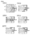
- FIG. 9 represents a configuration of a soft-switching inverter 101 X of a reference example.
- FIG. 1 represents a configuration of a soft-switching inverter according to an embodiment of the present invention.
- a soft-switching inverter (power conversion apparatus) 101 includes power supply terminals TP, TCP, TCN and TN, an AC output terminal TOUT, main switches Gp and Gn, main diodes Dp and Dn, snubber capacitors Crp and Crn, snubber diodes Drp and Drn, auxiliary switches Srp and Srn, auxiliary reactors Lrp and Lrn, a control circuit 11 , and a protection circuit 51 .
- Protection circuit 51 includes transformers Trp and Trn, and clamp diodes Dfp and Dfn.
- Transformer Trp includes a primary winding Ls 1 and a secondary winding Lf 1 .
- Transformer Trn includes a first primary winding Ls 2 and a secondary winding Lf 2 .
- Soft-switching inverter 101 may be configured to include DC power supplies Vp and Vn.
- Main switches Gp and Gn are IGBTs (Insulated Gate Bipolar Transistors), for example.
- Auxiliary switches Srp and Srn are reverse blocking thyristors, for example.
- DC power supplies Vp and Vn are connected in series.
- DC power supply Vp includes a positive electrode connected to power supply terminal TP, and a negative electrode connected to power supply terminals TCP and TCN.
- DC power supply Vn includes a positive electrode connected to the negative electrode of DC power supply Vp and power supply terminals TCP and TCN, and a negative electrode connected to power supply terminal TN.
- Main switch Gp includes a collector coupled to the positive electrode of DC power supply Vp, and an emitter connected to the load via AC output terminal TOUT.
- main switch Gp includes a collector connected to power supply terminal TP, and an emitter connected to the first end of primary winding Ls 1 of transformer Tr.
- Main diode Dp is connected in parallel with main switch Gp so as to have a conducting direction opposite to that of main switch Gp.
- main diode Dp includes a cathode connected to the collector of main switch Gp, and an anode connected to the emitter of main switch Gp.
- Snubber capacitor Crp is connected in parallel with main switch Gp and main diode Dp.
- Snubber diode Drp is connected in parallel with main switch Gp and main diode Dp and in series with snubber capacitor Crp so as to have a conducting direction identical to that of main switch Gp.
- snubber diode Drp includes an anode connected to a second end of snubber capacitor Crp and a second end of auxiliary reactor Lrp, and a cathode connected to the emitter of main switch Gp and the anode of main diode Dp.
- Auxiliary switch Srp and auxiliary reactor Lrp are connected between the connection node of DC power supply Vp and DC power supply Vn, i.e. power supply terminal TCP, and the connection node of snubber capacitor Crp and snubber diode Drp, and in series with each other.
- auxiliary switch Srp includes an anode connected to power supply terminal TCP, and a cathode connected to the first end of auxiliary reactor Lrp.
- Auxiliary reactor Lrp includes a first end connected to the cathode of auxiliary switch Srp and a second end connected to the connection node of snubber capacitor Crp and snubber diode Drp.
- Main switch Gn includes a collector coupled to the emitter of main switch Gp, and an emitter coupled to the negative electrode of DC power supply Vn, and is provided so as to have a conducting direction identical to that of main switch Gp.
- main switch Gn includes a collector connected to the second end of primary winding Ls 2 of transformer Tr, and an emitter connected to power supply terminal TN.
- Main diode Dn is connected in parallel with main switch Gn so as to have a conducting direction opposite to that of main switch Gn.
- main diode Dn includes a cathode connected to the collector of main switch Gn, and an anode connected to the emitter of main switch Gn.
- Snubber capacitor Crn is connected in parallel with main switch Gn and main diode Dn.
- Snubber diode Drn is connected in parallel with main switch Gn and main diode Dn, and in series with snubber capacitor Crn so as to have a conducting direction identical to that of main switch Gn.
- snubber diode Drn includes a cathode connected to the first end of snubber capacitor Crn and the second end of auxiliary reactor Lrn, and an anode connected to the collector of main switch Gn and the cathode of main diode Dn.
- Auxiliary switch Srn and auxiliary reactor Lrn are connected between the connection node of DC power supplies Vp and Vn and auxiliary switch Srp, i.e. power supply terminal TCN, and the connection node of snubber capacitor Crn and snubber diode Drn, and in series with each other.
- auxiliary switch Srn includes a cathode connected to power supply terminal TCN, and an anode connected to the first end of auxiliary reactor Lrn.
- Auxiliary reactor Lrn includes a first end connected to the anode of auxiliary switch Srn, and a second end connected to the connection node of snubber capacitor Crn and snubber diode Drn.
- Protection circuit 51 is connected between the emitter of main switch Gp and the collector of main switch Gn.
- primary windings Ls 1 and Ls 2 are connected between the emitter of main switch Gp and the collector of main switch Gn.
- primary winding Ls 1 includes a first end connected to the emitter of main switch Gp and the cathode of snubber diode Drp, and a second end connected to AC output terminal TOUT and the first end of primary winding Ls 2 .
- Primary winding Ls 2 includes a first end connected to AC output terminal TOUT and the second end of primary winding Ls 1 , and a second end connected to the collector of main switch Gn and the anode of snubber diode Drn.
- Primary windings Ls 1 and Ls 2 have the same winding direction.
- Secondary winding Lf 1 is connected between the positive electrode of DC power Vp and the connection node between DC power supply Vp and DC power supply Vn, and is magnetically coupled to primary winding Ls 1 .
- secondary winding Lf 1 includes a first end connected to the anode of clamp diode Dfp, and a second end connected to power supply terminal TCP.
- Secondary winding Lf 1 has a winding direction opposite to that of primary winding Ls 1 .
- the turns ratio of the primary winding to the secondary winding of transformer Trp is 1:n, and n>2, for example.
- Secondary winding Lf 2 is connected between the connection node of DC power supply Vp and DC power supply Vn, and the negative electrode of DC power supply Vn, and magnetically coupled to primary winding Ls 2 .
- secondary winding Lf 2 includes a first end connected to the anode of clamp diode Dfn, and a second end connected to power supply terminal TCN.
- Secondary winding Lf 1 has a winding direction opposite to that of primary winding Ls 2 .
- the turns ratio of the primary winding to the secondary winding of transformer Trn is 1:n, and n>2, for example.
- Clamp diode Dfp is connected between the positive electrode of DC power supply Vp, and the connection node of DC power supplies Vp and Vn, and in series with secondary winding Lf 1 .
- clamp diode Dfp includes a cathode connected to power supply terminal TP, and an anode connected to the first end of secondary winding Lf 1 .
- Clamp diode Dfn is connected between the connection node of DC power supplies Vp and Vn, and the negative electrode of DC power supply Vn, and in series with secondary winding Lf 2 .
- clamp diode Dfn includes a cathode connected to power supply terminal TCN, and an anode connected to the first end of secondary winding Lf.
- the switching of DC power supplied from DC power supplies through main switches Gp and Gn that are the main arms causes the DC power supplied from DC power supply Vp and DC power supply Vn to be converted into AC power, and then supplied to a load via AC output terminal TOUT.
- Snubber capacitor Crp is provided to prevent voltage from being applied to main switch Gp when main switch Gp is turned OFF.
- Snubber capacitor Crn is provided to prevent voltage from being applied to main switch Gn when main switch Gn is turned OFF.
- Control circuit 11 controls the switching of main switches Gp and Gn and auxiliary switches Srp and Srn.
- Protection circuit 51 has a current path PT 1 between the positive electrode of DC power supply Vp and the connection node of DC power supplies Vp and Vn. Protection circuit 51 also has a current path PT 2 between the connection node of DC power supplies Vp and Vn and the negative electrode of DC power supply Vn.
- Protection circuit 51 uses transformers Trp and Trn to suppress the maximum voltage applied to main switches Gp and Gn to a maximum value VM that is lower than 1.5 times the sum of the output voltages from DC power supplies Vp and Vn.
- FIGS. 2 and 3 represent in time series the flow of current during power conversion by the soft-switching inverter according to an embodiment of the present invention.
- FIG. 4 represents the switch control procedures during power conversion by the soft-switching inverter according to an embodiment of the present invention.
- DC power supply Vp provides an output voltage of Vp
- DC power supply Vn provides an output voltage of Vn.
- the horizontal axis in FIG. 4 represents time. Each number in the “positive period” along the horizontal axis represents corresponding steps shown in FIGS. 2 and 3 .
- step S 1 first the state (step S 1 ) will be described where main switch Gp is controlled to be turned on, main switch Gn is controlled to be turned off, and auxiliary switches Srp and Srn are controlled to be turned off, so that current flows from DC power supply Vp to the load through main switch Gp.
- main switch Gp is controlled to be turned off. This causes commutation of the current from DC power supply Vp to snubber capacitor Crp. Accordingly, snubber capacitor Crp is charged.
- main diode Dn is rendered conductive. Conduction of main diode Dn causes the current from DC power supply Vn to flow to the load through main diode Dn (step S 2 ).
- snubber capacitor Crp is charged by the resonant current of snubber capacitor Crp with the exciting inductance of primary windings Ls 1 and Ls 2 of transformers Trp and Trn.
- a voltage corresponding to the difference between the output voltages (Vp+Vn) of DC power supplies Vp and Vn and a voltage Vc at snubber capacitor Crp is applied to the series circuit of primary winding Ls 1 of transformer Trp and primary winding Ls 2 of transformer Trn.
- Primary windings Ls 1 and Ls 2 will each carry 1 ⁇ 2 the aforementioned differential voltage.
- the value of the voltage VL applied to primary windings Ls 1 and Ls 2 is represented by equation (1) set forth below.
- step S 3 current flows as indicated by the broken line shown at step S 3 in FIG. 2 .
- the current flowing to snubber capacitor Crp becomes zero, so that snubber capacitor Crp is no longer charged. Accordingly, voltage Vc at snubber capacitor Crp is clamped at the maximum value VM of voltage Vc. Then, when the current flowing through clamp diodes Dfp and Dfn is reduced to eventually become zero, clamp diodes Dfp and Dfn are rendered OFF.
- the commutation through current paths PT 1 and PT 2 ends (step S 3 ).
- main switch Gn is controlled to be turned on.
- main switch Gn is not rendered conductive since the current from main diode Dn to the load has a current polarity opposite to the conducting direction of main switch Gn. Therefore, current will continuously flow towards the load through main diode Dn (step S 4 ). In other words, current does not flow through main switch Gn when main switch Gn is controlled to be turned on. Accordingly, zero current switching is realized.
- auxiliary switch Srn is controlled to be turned on. Accordingly, discharging starts at snubber capacitor Crn. When discharging is completed and the voltage at snubber capacitor Crn becomes zero, snubber diode Drn is rendered conductive (step S 5 ).
- snubber diode Drn causes voltage from DC power supply Vn to be applied to auxiliary reactor Lrn. Accordingly, the current flowing through auxiliary switch Srn is reduced to eventually become zero. In response, auxiliary switch Srn and snubber diode Drn are both turned OFF (step S 6 ).
- main switch Gn is controlled to be turned off.
- main switch Gn is controlled to be turned off (step S 7 ).
- main switch Gp is controlled to be turned on. This causes commutation of the current from main diode Dn to main switch Gp.
- the current flowing from DC power supply Vp through main switch Gp increases to become equal to the load current, the current flowing through main diode Dn becomes zero at the same time, so that main diode Dn is turned off.
- the commutation is completed.
- step S 8 the current flowing from DC power supply Vp through main switch Gp flows towards snubber capacitor Crn.
- main diode Dn does not exhibit switching loss since no voltage is applied thereto. Accordingly, zero volt switching is realized (step S 8 ).
- snubber capacitor Crn is charged by the resonant current of snubber capacitor Crn and the exciting inductance of primary windings Ls 1 and Ls 2 of transformer Tr.
- the value of the voltage VL applied to primary windings Ls 1 and Ls 2 is represented by equation (3) set forth below.
- step S 9 current flows as indicated by the broken line shown at step S 9 in FIG. 3 .
- the current flowing to snubber capacitor Crn becomes zero, so that snubber capacitor Crn is no longer charged. Accordingly, voltage Vc at snubber capacitor Crn is clamped at VM. Then, when the current flowing through clamp diodes Dfp and Dfn is reduced to eventually become zero, clamp diodes Dfp and Dfn are rendered OFF.
- the commutation through current paths PT 1 and PT 2 ends (step S 9 ).
- step S 10 the current from DC power supply Vp flows through main switch Gp to the load.
- auxiliary switch Srp is controlled to be turned on. Accordingly, discharging starts at snubber capacitor Crp. When discharging is completed and the voltage at snubber capacitor Crp becomes zero, snubber diode Drp is rendered conductive (step S 11 ).
- snubber diode Drp causes voltage from DC power supply Vp to be applied to auxiliary reactor Lrp. Accordingly, the current flowing through auxiliary switch Srp is reduced to eventually become zero. In response, auxiliary switch Srp and snubber diode Drp are both turned OFF, returning to the state of step S 1 (step S 12 ).
- VM becomes less than or equal to 1.5 times Vdc. Moreover, since VM ⁇ (Vp+Vn) by increasing n, voltage Vc at the snubber capacitor can be suppressed to a value infinitely close to power supply voltage Vdc.
- step S 3 and step S 4 by the soft-switching inverter according to an embodiment of the present invention will be described in detail hereinafter.
- FIG. 5 represents the current flow in time series at step S 3 and step S 4 by the soft-switching inverter according to an embodiment of the present invention.
- FIG. 6 is a waveform diagram of voltage and current at step S 3 and step S 4 by the soft-switching inverter according to an embodiment of the present invention.
- FIG. 5 represents an equivalent circuit of soft-switching inverter 101 at step S 3 and step S 4 .
- this equivalent circuit any circuit not conducting at step S 3 and step S 4 will not be depicted.
- the section of transformer Tr is illustrated, divided into an ideal transformer and exciting inductance that is present in parallel at each winding.
- Lsid 1 , Lsid 2 are primary windings of an ideal transformer.
- Lfid 1 , Lfid 2 are secondary windings of an ideal transformer.
- L 1 is the exciting inductance at the primary side of transformer Tr.
- L 2 is the exciting inductance at the secondary side of transformer Tr. Description is based on the assumption that the turns ratio of transformer Tr is 1:4.
- Voltage Vc is the voltage at snubber capacitor Crp.
- Voltage V 1 is the voltage at the primary winding of transformer Tr.
- Voltage V 2 is the voltage at the secondary winding of transformer Tr. The direction of each arrow corresponds to “positive”.
- Step S 3 will be described, divided into three modes 1-3 in time series. Specifically, mode 1 corresponds to the state of initiating step S 3 ; mode 2 corresponds to the state after clamp diodes Dfp and Dfn are turned on; and mode 3 corresponds to the state after snubber diode Drp is turned off.
- step S 3 V 2 ⁇ 0 since voltage Vc is zero. Therefore, current will not flow through the ideal transformer since clamp diodes Dfp and Dfn are not conducting. Meanwhile, resonant current I 3 of exciting inductance L 1 and snubber capacitor Crp flows through exciting inductance L 1 . Snubber capacitor Crp is charged by the flow of resonant current I 3 . Accordingly, voltage Vc at snubber capacitor Crp increases.
- clamp diodes Dfp and Dfn are rendered conductive. Conduction of clamp diodes Dfp and Dfn causes currents I 21 and I 22 to flow through secondary windings Lfid 1 and Lfid 2 of the ideal transformer.
- current I 1 that is four times currents I 21 and I 22 flows through primary windings Lsid 1 and Lsid 2 of the ideal transformer.
- current I 1 functions to cancel the charging current of snubber capacitor Crp, i.e. current I 3 .
- FIGS. 7 and 8 represent in time series the flow of current during power conversion by the soft-switching inverter according to an embodiment of the present invention.
- DC power supply Vp provides an output voltage of Vp
- DC power supply Vn provides an output voltage of Vn.
- the horizontal axis in FIG. 4 represents time. Each number in the “negative period” along the horizontal axis represents corresponding steps shown in FIGS. 7 and 8 .
- step S 21 first the state (step S 21 ) will be described where main switch Gn is controlled to be turned on, main switch Gp is controlled to be turned off, and auxiliary switches Srn and Srp are controlled to be turned off, so that current flows from DC power supply Vn to the load through main switch Gn.
- main switch Gn is controlled to be turned off. This causes commutation of the current from the load to snubber capacitor Crn. Accordingly, snubber capacitor Crn is charged.
- main diode Dp is rendered conductive. Conduction of main diode Dp causes the current from the load to flow to DC power supply Vp through main diode Dp (step S 22 ).
- snubber capacitor Crn is charged by the resonant current of snubber capacitor Crn with the exciting inductance of primary windings Ls 1 and Ls 2 of transformer Tr.
- Primary windings Ls 1 and Ls 2 will each carry 1 ⁇ 2 the aforementioned differential voltage.
- the value of the voltage VL applied to primary windings Ls 1 and Ls 2 is represented by equation (5) set forth below.
- step S 23 current flows as indicated by the broken line shown at step S 23 in FIG. 5 .
- the current flowing to snubber capacitor Crn becomes zero, so that snubber capacitor Crn is no longer charged. Accordingly, voltage Vc at snubber capacitor Crn is clamped at VM. Then, when the current flowing through clamp diodes Dfp and Dfn is reduced to eventually become zero, clamp diodes Dfp and Dfn are rendered OFF.
- the commutation through current paths PT 1 and PT 2 ends (step S 23 ).
- main switch Gp is controlled to be turned on.
- main switch Gp is not rendered conductive since the current from the load to main diode Dp has a current polarity opposite to the conducting direction of main switch Gp. Therefore, current will continuously flow towards DC power supply Vp through main diode Dp (step S 24 ). In other words, current does not flow through main switch Gp when main switch Gp is controlled to be turned on. Accordingly, zero current switching is realized.
- auxiliary switch Srp is controlled to be turned on. Accordingly, discharging starts at snubber capacitor Crp. When discharging is completed and the voltage at snubber capacitor Crp becomes zero, snubber diode Drp is rendered conductive (step S 25 ).
- snubber diode Drp causes voltage from DC power supply Vp to be applied to auxiliary reactor Lrp. Accordingly, the current flowing through auxiliary switch Srp is reduced to eventually become zero. In response, auxiliary switch Srp and snubber diode Drp are both turned OFF (step S 26 ).
- main switch Gp is controlled to be turned off.
- main switch Gp is controlled to be turned off (step S 27 ).
- main switch Gn is controlled to be turned on. This causes commutation of the current from main diode Dp to main switch Gn.
- the current flowing from DC power supply Vn through main switch Gn increases to become equal to the load current, the current flowing through main diode Dp becomes zero at the same time, so that main diode Dp is turned off.
- the commutation is completed.
- step S 28 snubber diode Drp is rendered conductive. Since the charge in snubber capacitor Crp is zero at this stage, the current flowing from DC power supply Vp flows towards snubber capacitor Crp. In other words, main diode Dp does not exhibit switching loss since no voltage is applied thereto. Accordingly, zero volt switching is realized (step S 28 ).
- snubber capacitor Crp is charged by the resonant current of snubber capacitor Crn and the exciting inductance of primary windings Ls 1 and Ls 2 of transformer Tr.
- the value VL of the voltage applied to primary windings Ls 1 and Ls 2 is represented by equation (7) set forth below.
- step S 29 current flows as indicated by the broken line shown at step S 29 in FIG. 6 .
- the current flowing to snubber capacitor Crp becomes zero, so that snubber capacitor Crp is no longer charged. Accordingly, voltage Vc at snubber capacitor Crp is clamped at VM. Then, when the current flowing through clamp diodes Dfp and Dfn is reduced to eventually become zero, clamp diodes Dfp and Dfn are rendered OFF.
- the commutation through current paths PT 1 and PT 2 ends (step S 29 ).
- step S 30 the current from the load flows through main switch Gn to DC power supply Vn.
- auxiliary switch Srn is controlled to be turned on. Accordingly, discharging starts at snubber capacitor Crn. When discharging is completed and the voltage at snubber capacitor Crn becomes zero, snubber diode Drn is rendered conductive (step S 31 ).
- snubber diode Drn causes voltage from DC power supply Vn to be applied to auxiliary reactor Lrn. Accordingly, the current flowing through auxiliary switch Srn is reduced to eventually become zero. In response, auxiliary switch Srn and snubber diode Drn are both turned OFF, returning to the state of step S 21 (step S 32 ).
- Soft-switching inverter 101 repeats the operation of steps S 1 -S 12 shown in FIGS. 2 and 3 as the operation in the positive period, and repeats the operation of steps S 21 -S 32 shown in FIGS. 7 and 8 as the operation in a negative period. By alternately performing such positive period operation and negative period operation, AC power is fed to the load.
- soft-switching inverter 101 To facilitate the understanding of soft-switching inverter 101 according to an embodiment of the present invention, a soft-switching inverter 101 X of a reference example will be described for comparison.
- FIG. 9 is a diagram representing a configuration of soft-switching inverter 101 X as a reference example.
- Soft-switching inverter 101 X will be briefly described as compared to soft-switching inverter 101 according to an embodiment.
- Soft-switching inverter 101 X includes a protection circuit 51 X instead of protection circuit 51 of soft-switching inverter 101 .
- Protection circuit 51 X includes a transformer TrX, and a clamp diode Df.
- Transformer TrX includes primary windings Ls 1 and Ls 2 , and a secondary winding Lf.
- soft-switching inverter 101 has clamp diode Df divided into two clamp diodes Df 1 and Df 2 , and similarly has secondary winding Lf of transformer Tr divided into two secondary windings Lf 1 and Lf 2 .
- Secondary winding Lf 1 and clamp diode Dfp are connected in series between power supply voltage terminals TP and TCP.
- Secondary winding Lf 2 and clamp diode Dfn are connected in series between power supply terminals TCN and TN.
- the remaining elements are similar to those of soft-switching inverter 101 . Therefore, description thereof will not be repeated.
- protection circuit 51 X of the reference example renders clamp diode Df conductive provided on current path PT to complete charging of the snubber capacitor (Cs 1 , Cs 2 ), when the snubber capacitor (Cs 1 , Cs 2 ) is charged to a level greater than or equal to a predetermined voltage.
- Maximum voltage VM applied to snubber capacitor Crp (Crn) of the reference example becomes (1+2/n) Vdc, likewise with the discussion set forth above.
- Maximum voltage VM applied to snubber capacitor Crp (Crn) according to an embodiment becomes (1+1/n) Vdc by equations (4) and (6).
- the maximum voltage applied to the snubber capacitor of soft-switching inverter 101 X takes a value lower than 2 Vdc.
- the maximum voltage applied to the snubber capacitor of soft-switching inverter 101 according to the present embodiment can be suppressed to take a value lower than 1.5 Vdc. It is therefore appreciated that the voltage suppression effect is higher than that of the reference example.
- the maximum value of the applied voltage can be reduced at soft-switching inverter 101 X of the reference example by selecting a large turns ratio n.
- the voltage at the secondary side of the transformer becomes extremely high, leading to the requirement of elements of high breakdown voltage for both the transformer and clamp diode. This is not practical since the cost will be increased.
- the maximum voltage of the snubber capacitor can be reduced to allow the size and cost of the device to be reduced.
- the value of the maximum voltage applied to main switches Gp and Gn, main diodes Dp and Dn, and clamp diodes Drp and Drn can be also reduced.
- soft-switching inverter 101 of the present embodiment is a power conversion apparatus for converting DC power, supplied from a DC power supply Vp having a first electrode and a second electrode and from a DC power supply Vn having a first electrode connected to the second electrode of DC power supply Vp and a second electrode, into AC power, and supplying the AC power to a load; including: a main switch Gp having a first end coupled to the first electrode of DC power supply Vp and a second end coupled to the load; a main diode Dp connected in parallel with main switch Gp, so as to have a conducting direction opposite to the conducting direction of main switch Gp; a snubber capacitor Crp connected in parallel with main switch Gp and main diode Dp; a snubber diode Drp connected in series with snubber capacitor Crp and connected between snubber capacitor Crp and the second end of main switch Gp so as to have a conducting direction identical to the conducting direction of main switch G
- Protection circuit 51 includes transformers Trp and Trn, and clamp diodes Dfp and Dfp.
- Transformer Trp includes a primary winding Ls 1 connected between the second end of main switch Gp and the load, and a secondary winding Lf 1 connected between the first electrode of DC power supply Vp and the second electrode of DC power supply Vp, and magnetically coupled to the primary winding.
- Transformer Trn includes a primary winding Ls 2 connected between the first end of main switch Gn and the load, and a secondary winding Lf 2 connected between the first electrode of DC power supply Vn and the second electrode of DC power supply Vn, and magnetically coupled to the primary winding.
- Secondary winding Ls 1 and clamp diode Dfp are connected in series between the first electrode of DC power supply Vp and the second electrode of DC power supply Vp.
- Secondary winding Ls 2 and clamp diode Dfn are connected in series between the first electrode of DC power supply Vn and the second electrode of DC power supply Vn.
- Secondary winding Ls 1 and clamp diode Dfp are connected in series.
- Primary winding Lf 1 and primary winding Lf 2 are connected in series. The connection node of primary winding Lf 1 and primary winding Lf 2 is connected to the load.
- soft-switching inverter 101 further includes a control circuit 11 for controlling main switch Gp, main switch Gn, auxiliary switch Srp and auxiliary switch Srn to be turned ON and OFF.
- control circuit 11 discharges snubber capacitor Crn by controlling auxiliary switch Srn to be turned on while main diode Dn is ON during a positive period in which current flows from the power conversion apparatus to the load, and discharges snubber capacitor Crp by controlling auxiliary switch Srp to be turned on while main diode Dp is ON during a negative period in which current flows from the load to the power conversion apparatus.
- control circuit 11 controls main switch Gn to be turned on at an elapse of a predetermined time from main switch Gn being turned off, controls auxiliary switch Srn to be turned on at an elapse of a predetermined time from main switch Gn being turned off, controls main switch Gn to be turned off at an elapse of a predetermined time from auxiliary switch Srn being turned on, controls main switch Gp to be turned on at an elapse of a predetermined time from main switch Gn being turned off, controls auxiliary switch Srp to be turned on at an elapse of a predetermined time from main switch Gp being turned on, and controls main switch Gp to be turned off at an elapse of a predetermined time from auxiliary switch Srp being turned on.
Landscapes
- Engineering & Computer Science (AREA)
- Power Engineering (AREA)
- Dc-Dc Converters (AREA)
- Inverter Devices (AREA)
Abstract
Description
VL={(Vp+Vn)−Vc}/2=(Vdc−Vc)/2 (1)
VM=(1+1/n)×(Vp+Vn)=(1+1/n)×Vdc (2)
VL={(Vp+Vn)−Vc}/2=(Vdc−Vc)/2 (3)
VM=(1+1/n)×(Vp+Vn)=(1+1/n)×Vdc (4)
VL={(Vn+Vp)−Vc}/2=(Vdc−Vc)/2 (5)
VM=(1+1/n)×(Vn+Vp)=(1+1/n)×Vdc (6)
VL={(Vn+Vp)−Vc}/2=(Vdc−Vc)/2 (7)
VM=(1+1/n)×(Vn+Vp)=(1+1/n)×Vdc (8)
Claims (4)
Applications Claiming Priority (1)
| Application Number | Priority Date | Filing Date | Title |
|---|---|---|---|
| PCT/JP2012/055377 WO2013128632A1 (en) | 2012-03-02 | 2012-03-02 | Power conversion device |
Publications (2)
| Publication Number | Publication Date |
|---|---|
| US20140346880A1 US20140346880A1 (en) | 2014-11-27 |
| US9621026B2 true US9621026B2 (en) | 2017-04-11 |
Family
ID=49081876
Family Applications (1)
| Application Number | Title | Priority Date | Filing Date |
|---|---|---|---|
| US14/373,708 Active 2033-05-23 US9621026B2 (en) | 2012-03-02 | 2012-03-02 | Power conversion apparatus |
Country Status (5)
| Country | Link |
|---|---|
| US (1) | US9621026B2 (en) |
| EP (1) | EP2822169B1 (en) |
| JP (1) | JP5749853B2 (en) |
| CN (1) | CN104145413B (en) |
| WO (1) | WO2013128632A1 (en) |
Families Citing this family (2)
| Publication number | Priority date | Publication date | Assignee | Title |
|---|---|---|---|---|
| CN104838580A (en) * | 2013-07-24 | 2015-08-12 | 株式会社小松制作所 | Hybrid work machine |
| US9438099B2 (en) * | 2014-01-09 | 2016-09-06 | Fred O. Barthold | Harmonic displacement reduction |
Citations (2)
| Publication number | Priority date | Publication date | Assignee | Title |
|---|---|---|---|---|
| WO2010125630A1 (en) | 2009-04-27 | 2010-11-04 | 東芝三菱電機産業システム株式会社 | Power converter |
| WO2011036912A1 (en) | 2009-09-24 | 2011-03-31 | 東芝三菱電機産業システム株式会社 | Power conversion device |
Family Cites Families (3)
| Publication number | Priority date | Publication date | Assignee | Title |
|---|---|---|---|---|
| JPH10285953A (en) * | 1997-04-08 | 1998-10-23 | Fuji Electric Co Ltd | Power converter |
| JP3450690B2 (en) * | 1998-01-20 | 2003-09-29 | 三菱電機株式会社 | Power system compensation controller |
| JP2002272141A (en) * | 2001-03-09 | 2002-09-20 | Hitachi Metals Ltd | Bridged converter and dc-dc converter therewith |
-
2012
- 2012-03-02 JP JP2014501929A patent/JP5749853B2/en not_active Expired - Fee Related
- 2012-03-02 WO PCT/JP2012/055377 patent/WO2013128632A1/en active Application Filing
- 2012-03-02 US US14/373,708 patent/US9621026B2/en active Active
- 2012-03-02 EP EP12869748.9A patent/EP2822169B1/en active Active
- 2012-03-02 CN CN201280071073.9A patent/CN104145413B/en active Active
Patent Citations (4)
| Publication number | Priority date | Publication date | Assignee | Title |
|---|---|---|---|---|
| WO2010125630A1 (en) | 2009-04-27 | 2010-11-04 | 東芝三菱電機産業システム株式会社 | Power converter |
| US8605470B2 (en) | 2009-04-27 | 2013-12-10 | Toshiba Mitsubishi-Electric Industrial Systems Corporation | Power converter performing soft switching |
| WO2011036912A1 (en) | 2009-09-24 | 2011-03-31 | 東芝三菱電機産業システム株式会社 | Power conversion device |
| US8508962B2 (en) | 2009-09-24 | 2013-08-13 | Toshiba Mitsubishi-Electric Industrial Systems Corporation | Power conversion apparatus |
Non-Patent Citations (2)
| Title |
|---|
| International Search Report Issued Jun. 5, 2012 in PCT/JP12/055377 Filed Mar. 2, 2012. |
| U.S. Appl. No. 14/376,057, filed Jul. 31, 2014, Hosokawa, et al. |
Also Published As
| Publication number | Publication date |
|---|---|
| US20140346880A1 (en) | 2014-11-27 |
| JP5749853B2 (en) | 2015-07-15 |
| WO2013128632A1 (en) | 2013-09-06 |
| CN104145413A (en) | 2014-11-12 |
| JPWO2013128632A1 (en) | 2015-07-30 |
| EP2822169B1 (en) | 2017-10-18 |
| CN104145413B (en) | 2017-07-14 |
| EP2822169A4 (en) | 2016-04-20 |
| EP2822169A1 (en) | 2015-01-07 |
Similar Documents
| Publication | Publication Date | Title |
|---|---|---|
| TWI661634B (en) | Modular power system | |
| EP3257146B1 (en) | Dc-dc converter | |
| US9748848B2 (en) | Modular multilevel DC/DC converter for HVDC applications | |
| US20170179836A1 (en) | Power conversion device | |
| US20110096581A1 (en) | Inverter and method for operating the inverter | |
| US8508962B2 (en) | Power conversion apparatus | |
| US20050180176A1 (en) | Welding set with quasi-resonant soft-switching inverter | |
| JP5284465B2 (en) | Power converter | |
| JP6140007B2 (en) | Power converter | |
| JP2013074767A (en) | Dc/dc converter | |
| US9621026B2 (en) | Power conversion apparatus | |
| WO2013118678A1 (en) | Power conversion device and method for driving same | |
| CN116155106A (en) | Isolated bipolar output self-equalizing DC-DC converter | |
| US20230322105A1 (en) | Charging device and method for operating the charging device | |
| KR20180091543A (en) | Power factor correction converter | |
| WO2018108143A1 (en) | Modular power supply system | |
| US9281740B2 (en) | Power conversion apparatus | |
| JP5325991B2 (en) | Power converter | |
| Qi et al. | Capacitor voltage balancing control for 3LNPC LLC resonant converter | |
| Nayak et al. | Soft-switched Single-stage Isolated AC-DC Converter for High Power Applications | |
| Lin et al. | Half-bridge ZVS converter with three resonant tanks |
Legal Events
| Date | Code | Title | Description |
|---|---|---|---|
| AS | Assignment |
Owner name: TOSHIBA MITSUBISHI-ELECTRIC INDUSTRIAL SYSTEMS COR Free format text: ASSIGNMENT OF ASSIGNORS INTEREST;ASSIGNOR:HOSOKAWA, YASUHIKO;REEL/FRAME:033362/0832 Effective date: 20140610 |
|
| STCF | Information on status: patent grant |
Free format text: PATENTED CASE |
|
| MAFP | Maintenance fee payment |
Free format text: PAYMENT OF MAINTENANCE FEE, 4TH YEAR, LARGE ENTITY (ORIGINAL EVENT CODE: M1551); ENTITY STATUS OF PATENT OWNER: LARGE ENTITY Year of fee payment: 4 |
|
| AS | Assignment |
Owner name: TMEIC CORPORATION, JAPAN Free format text: CHANGE OF NAME;ASSIGNOR:TOSHIBA MITSUBISHI-ELECTRIC INDUSTRIAL SYSTEMS CORPORATION;REEL/FRAME:067244/0359 Effective date: 20240401 |
|
| MAFP | Maintenance fee payment |
Free format text: PAYMENT OF MAINTENANCE FEE, 8TH YEAR, LARGE ENTITY (ORIGINAL EVENT CODE: M1552); ENTITY STATUS OF PATENT OWNER: LARGE ENTITY Year of fee payment: 8 |