WO2010122657A1 - 固体撮像装置およびその製造方法 - Google Patents
固体撮像装置およびその製造方法 Download PDFInfo
- Publication number
- WO2010122657A1 WO2010122657A1 PCT/JP2009/058127 JP2009058127W WO2010122657A1 WO 2010122657 A1 WO2010122657 A1 WO 2010122657A1 JP 2009058127 W JP2009058127 W JP 2009058127W WO 2010122657 A1 WO2010122657 A1 WO 2010122657A1
- Authority
- WO
- WIPO (PCT)
- Prior art keywords
- film
- pixel
- layer film
- imaging device
- solid
- Prior art date
- Legal status (The legal status is an assumption and is not a legal conclusion. Google has not performed a legal analysis and makes no representation as to the accuracy of the status listed.)
- Ceased
Links
Images













Classifications
-
- H—ELECTRICITY
- H10—SEMICONDUCTOR DEVICES; ELECTRIC SOLID-STATE DEVICES NOT OTHERWISE PROVIDED FOR
- H10F—INORGANIC SEMICONDUCTOR DEVICES SENSITIVE TO INFRARED RADIATION, LIGHT, ELECTROMAGNETIC RADIATION OF SHORTER WAVELENGTH OR CORPUSCULAR RADIATION
- H10F39/00—Integrated devices, or assemblies of multiple devices, comprising at least one element covered by group H10F30/00, e.g. radiation detectors comprising photodiode arrays
- H10F39/011—Manufacture or treatment of image sensors covered by group H10F39/12
- H10F39/024—Manufacture or treatment of image sensors covered by group H10F39/12 of coatings or optical elements
-
- H—ELECTRICITY
- H10—SEMICONDUCTOR DEVICES; ELECTRIC SOLID-STATE DEVICES NOT OTHERWISE PROVIDED FOR
- H10F—INORGANIC SEMICONDUCTOR DEVICES SENSITIVE TO INFRARED RADIATION, LIGHT, ELECTROMAGNETIC RADIATION OF SHORTER WAVELENGTH OR CORPUSCULAR RADIATION
- H10F39/00—Integrated devices, or assemblies of multiple devices, comprising at least one element covered by group H10F30/00, e.g. radiation detectors comprising photodiode arrays
- H10F39/011—Manufacture or treatment of image sensors covered by group H10F39/12
- H10F39/014—Manufacture or treatment of image sensors covered by group H10F39/12 of CMOS image sensors
-
- H—ELECTRICITY
- H10—SEMICONDUCTOR DEVICES; ELECTRIC SOLID-STATE DEVICES NOT OTHERWISE PROVIDED FOR
- H10F—INORGANIC SEMICONDUCTOR DEVICES SENSITIVE TO INFRARED RADIATION, LIGHT, ELECTROMAGNETIC RADIATION OF SHORTER WAVELENGTH OR CORPUSCULAR RADIATION
- H10F39/00—Integrated devices, or assemblies of multiple devices, comprising at least one element covered by group H10F30/00, e.g. radiation detectors comprising photodiode arrays
- H10F39/10—Integrated devices
- H10F39/12—Image sensors
- H10F39/18—Complementary metal-oxide-semiconductor [CMOS] image sensors; Photodiode array image sensors
-
- H—ELECTRICITY
- H10—SEMICONDUCTOR DEVICES; ELECTRIC SOLID-STATE DEVICES NOT OTHERWISE PROVIDED FOR
- H10F—INORGANIC SEMICONDUCTOR DEVICES SENSITIVE TO INFRARED RADIATION, LIGHT, ELECTROMAGNETIC RADIATION OF SHORTER WAVELENGTH OR CORPUSCULAR RADIATION
- H10F39/00—Integrated devices, or assemblies of multiple devices, comprising at least one element covered by group H10F30/00, e.g. radiation detectors comprising photodiode arrays
- H10F39/80—Constructional details of image sensors
- H10F39/802—Geometry or disposition of elements in pixels, e.g. address-lines or gate electrodes
-
- H—ELECTRICITY
- H10—SEMICONDUCTOR DEVICES; ELECTRIC SOLID-STATE DEVICES NOT OTHERWISE PROVIDED FOR
- H10F—INORGANIC SEMICONDUCTOR DEVICES SENSITIVE TO INFRARED RADIATION, LIGHT, ELECTROMAGNETIC RADIATION OF SHORTER WAVELENGTH OR CORPUSCULAR RADIATION
- H10F39/00—Integrated devices, or assemblies of multiple devices, comprising at least one element covered by group H10F30/00, e.g. radiation detectors comprising photodiode arrays
- H10F39/80—Constructional details of image sensors
- H10F39/802—Geometry or disposition of elements in pixels, e.g. address-lines or gate electrodes
- H10F39/8023—Disposition of the elements in pixels, e.g. smaller elements in the centre of the imager compared to larger elements at the periphery
-
- H—ELECTRICITY
- H10—SEMICONDUCTOR DEVICES; ELECTRIC SOLID-STATE DEVICES NOT OTHERWISE PROVIDED FOR
- H10F—INORGANIC SEMICONDUCTOR DEVICES SENSITIVE TO INFRARED RADIATION, LIGHT, ELECTROMAGNETIC RADIATION OF SHORTER WAVELENGTH OR CORPUSCULAR RADIATION
- H10F39/00—Integrated devices, or assemblies of multiple devices, comprising at least one element covered by group H10F30/00, e.g. radiation detectors comprising photodiode arrays
- H10F39/80—Constructional details of image sensors
- H10F39/803—Pixels having integrated switching, control, storage or amplification elements
- H10F39/8037—Pixels having integrated switching, control, storage or amplification elements the integrated elements comprising a transistor
-
- H—ELECTRICITY
- H10—SEMICONDUCTOR DEVICES; ELECTRIC SOLID-STATE DEVICES NOT OTHERWISE PROVIDED FOR
- H10F—INORGANIC SEMICONDUCTOR DEVICES SENSITIVE TO INFRARED RADIATION, LIGHT, ELECTROMAGNETIC RADIATION OF SHORTER WAVELENGTH OR CORPUSCULAR RADIATION
- H10F39/00—Integrated devices, or assemblies of multiple devices, comprising at least one element covered by group H10F30/00, e.g. radiation detectors comprising photodiode arrays
- H10F39/80—Constructional details of image sensors
- H10F39/805—Coatings
-
- H—ELECTRICITY
- H10—SEMICONDUCTOR DEVICES; ELECTRIC SOLID-STATE DEVICES NOT OTHERWISE PROVIDED FOR
- H10F—INORGANIC SEMICONDUCTOR DEVICES SENSITIVE TO INFRARED RADIATION, LIGHT, ELECTROMAGNETIC RADIATION OF SHORTER WAVELENGTH OR CORPUSCULAR RADIATION
- H10F39/00—Integrated devices, or assemblies of multiple devices, comprising at least one element covered by group H10F30/00, e.g. radiation detectors comprising photodiode arrays
- H10F39/80—Constructional details of image sensors
- H10F39/803—Pixels having integrated switching, control, storage or amplification elements
Definitions
- the present invention relates to a solid-state imaging device and a manufacturing method thereof, and more particularly to a solid-state imaging device having a photoelectric conversion unit and an insulated gate field effect transistor unit and a manufacturing method thereof.
- Solid-state imaging devices having a plurality of photodiodes serving as incident light photoelectric conversion sections and MOS (Metal Oxide Semiconductor) transistors serving as insulated gate field effect transistor sections are disclosed in, for example, Japanese Patent Application Laid-Open Nos. 2004-228425 and 2008. -041958 and the like.
- Japanese Patent Application Laid-Open No. 2008-041958 discloses that the thickness of the antireflection film and the thickness of the sidewall cannot be controlled independently by the manufacturing method of Japanese Patent Application Laid-Open No. 2004-228425.
- an antireflection film and a sidewall are formed in the same process from three layers of insulating films of a lower layer, a middle layer and an upper layer.
- the refractive index and thickness of the antireflection film are controlled by two layers of the lower layer and the middle insulating film, and the thickness of the sidewall is controlled by three layers of the lower layer, the middle layer, and the upper layer. It is described in the above publication that each thickness can be controlled independently.
- the sidewall width follows the scaling law, but the thickness of the antireflection film does not follow the scaling law because the optimum structure is determined by the wavelength of the incident light.
- the thickness of the antireflection film is always the same as or thinner than the width of the sidewall. Therefore, when the width of the sidewall is reduced according to the scaling law, the thickness of the antireflection film needs to be reduced accordingly, so that there is a problem that the application of this technique becomes difficult as the transistor becomes finer.
- Japanese Patent Application Laid-Open No. 2008-041958 describes that the refractive index and thickness of the antireflection film are optimally controlled by two layers of a lower layer and a middle layer insulating film.
- the refractive index of the upper insulating film needs to be the same as the refractive index of the interlayer insulating film on the antireflection film. This is because when the refractive indexes of the interlayer insulating film and the upper insulating film are different from each other, the reflection occurring at the interface between them cannot be ignored.
- the antireflection film has three layers (or more) and the upper insulating film has a refractive index different from that of the interlayer insulating film, the technique of Japanese Patent Application Laid-Open No. 2008-041958 cannot be applied in principle. There is a problem that there are many restrictions on the antireflection film.
- the structure of the optimal antireflection film differs depending on the wavelength of incident light. For this reason, when a light receiving pixel is different for each of the three primary colors R (Red), G (Green), and B (Blue) as in a general imaging device, an antireflection film is optimized for each pixel. It is desirable.
- the antireflection film and the sidewall are formed in the same process, the antireflection film is the same for all the R, G, and B pixels due to the restriction of the sidewall. It becomes thickness. For this reason, optimization of the antireflection film must be performed for light of any wavelength of R, G, and B, and sufficient antireflection effect cannot be obtained for light of other wavelengths. There's a problem.
- the present invention has been made in view of the above problems, and its object is to provide a solid-state imaging device that can cope with miniaturization, has few restrictions on an antireflection film, and can optimize the antireflection effect for each pixel, and a method for manufacturing the same. Is to provide.
- a manufacturing method of a solid-state imaging device includes a plurality of photoelectric conversion units that form a plurality of pixels, an insulated gate field effect transistor unit, and each formed on each of the plurality of photoelectric conversion units.
- a method for manufacturing a solid-state imaging device including the plurality of first films which includes the following steps.
- a laminated film made of a plurality of insulating films is formed so as to cover the plurality of photoelectric conversion portions and the gate electrode layer of the insulated gate field effect transistor portion.
- the laminated film is left on each of the plurality of photoelectric conversion portions to form a lower layer film, and the laminated film is left on the side wall of the gate electrode layer.
- a sidewall insulating film is formed. Impurities are introduced into regions not covered with the gate electrode layer and the sidewall insulating film, thereby forming source / drain regions of the insulated gate field effect transistor.
- an upper layer film is formed at least on the lower layer film. At least one of the upper layer film and the lower layer film is etched so that the thicknesses of the first films on at least two of the plurality of photoelectric conversion units are different from each other.
- the width of the sidewall insulating film and the thickness of the first film can be controlled independently, it is easy to cope with miniaturization.
- the first film and the side wall insulating film are more first than the case where they are formed in the same process. There are fewer restrictions on the film.
- the upper layer film is formed, and at least one of the lower layer film and the upper layer film is removed, so that the antireflection effect is optimized for each pixel. Can do.
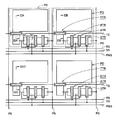
- FIG. 1 It is a top view which shows roughly the structure of the solid-state imaging device in Embodiment 1 of this invention.
- FIG. 1 It is a circuit diagram which shows the circuit structure of the solid-state imaging device shown in FIG.
- FIG. 1 It is a schematic sectional drawing which shows the 1st process of the manufacturing method of the solid-state imaging device in Embodiment 1 of this invention.
- the solid-state imaging device of the present embodiment has a plurality of pixels PX.
- the plurality of pixels PX include pixels that pick up light of different colors. For example, a pixel that picks up red light (R pixel), a pixel that picks up green light (G pixel), and a pixel that picks up blue light (G pixel) ( B pixels).
- Each of the plurality of pixels PX includes, for example, a photodiode PD as a photoelectric conversion unit, a transfer transistor TTR, a reset transistor RTR, an amplification transistor ATR, and a selection transistor STR.
- the photodiode PD has a p-type region and an n-type region that form a pn junction with each other.
- An antireflection film (not shown) is formed on the light incident side of the photodiode PD.
- This antireflection film preferably has a different structure (film thickness, film quality, etc.) depending on the color of light to be imaged.
- Each of the transfer transistor TTR, the reset transistor RTR, the amplification transistor ATR, and the selection transistor STR is an insulated gate field effect transistor, and is composed of, for example, an n-channel MOS transistor.
- Each of these transistors has a pair of n-type source / drain regions formed on the surface of the semiconductor substrate and a gate insulating film (gate oxide film) on the region of the semiconductor substrate sandwiched between the pair of source / drain regions. And a gate electrode layer formed with a gap therebetween. Side walls (side wall insulating films: not shown) are formed so as to cover the side walls of each gate electrode layer.
- the p-type region of the photodiode PD is connected to a ground potential, for example.
- the n-type region of the photodiode PD and the n-type source region of the transfer transistor TTR are electrically connected, and are formed by, for example, a common n-type region.
- the gate electrode layer of the transfer transistor TTR is electrically connected to the transfer signal line TS.
- the n-type drain region of the transfer transistor TTR and the n-type source region of the reset transistor RTR are electrically connected.
- the gate electrode layer of the reset transistor RTR is electrically connected to the reset signal line RS.
- the n-type drain region of the resetting transistor RTR and the n-type source region of the amplifying transistor ATR are electrically connected, and are formed by, for example, a common n-type region.
- a power supply line PWS is electrically connected to the n-type drain region of the resetting transistor RTR and the n-type source region of the amplifying transistor ATR.
- the gate electrode layer of the amplifying transistor ATR is electrically connected to the n-type drain region of the transfer transistor TTR and the n-type source region of the reset transistor RTR.
- the n-type drain region of the amplification transistor ATR and the n-type source region of the selection transistor STR are electrically connected, and are formed by, for example, a common n-type region.
- the gate electrode layer of the selection transistor STR is electrically connected to the selection signal line SS.
- the n-type drain region of the selection transistor STR is electrically connected to the vertical signal line PS.
- peripheral circuits for performing operations are formed. These peripheral circuits also include transistors, and these transistors are also formed of insulated gate field effect transistors.
- one reset transistor RTR, an amplification transistor ATR, and a selection transistor STR are provided for one set of diode portions each including one photodiode PD and transfer transistor TTR.
- a configuration in which one set of transistor groups is provided has been described, a configuration in which one set of the transistor groups is provided for a plurality of sets of the diode portions may be employed.
- one set of the transistor group may be shared by a plurality of sets of the diode portions connected in parallel.
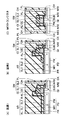
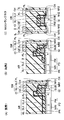
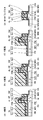
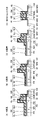
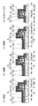
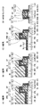
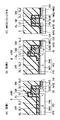
- Each pixel 1 shown in FIG. 3A to FIG. 11A corresponds to a cross section taken along the line IIIA-IIIA in FIG. 1, for example, and each pixel 2 shown in FIG. 3B to FIG. Corresponds to the cross section taken along the line IIIB-IIIB.
- Each of the MOS transistors shown in (C) of FIGS. 3 to 11 corresponds to, for example, a cross section taken along line IIIC-IIIC of FIG.
- an element isolation structure (not shown) and a p-type well region PW are formed on the surface of an n-type semiconductor substrate SUB made of, for example, silicon. Thereafter, by oxidizing the surface of the semiconductor substrate SUB, for example, a silicon oxide film GI is formed on the surface of the semiconductor substrate SUB. On the silicon oxide film GI, for example, a polycrystalline silicon film GE and a silicon oxide film CI are sequentially stacked.
- the silicon oxide film CI, the polycrystalline silicon film GE, and the silicon oxide film GI are patterned by a normal photolithography technique and etching technique.
- a stacked pattern composed of a gate insulating film GI made of, for example, a silicon oxide film, a gate electrode layer GE made of, for example, a polycrystalline silicon film, and a cap insulating film CI made of, for example, a silicon oxide film is formed into the pixels 1, 2 and It is formed in each MOS transistor.
- a photoresist pattern PR1 is formed on the surface of semiconductor substrate SUB by a normal photolithography technique.
- the photoresist pattern PR1 is formed so as to open on the portions where the photodiodes of the pixels 1 and 2 are formed and to cover the MOS transistors.
- ions such as arsenic (As) and phosphorus (P) are implanted into the surface of the semiconductor substrate SUB.
- an n-type region NR1 is formed on the surface of the semiconductor substrate SUB, and a photodiode PD is formed in a portion indicated by the region S by the n-type region NR1 and the p-type well region PW. Thereafter, photoresist pattern PR1 is removed by, for example, ashing.
- a photoresist pattern PR1A is formed on the surface of semiconductor substrate SUB by a normal photolithography technique.
- the photoresist pattern PR1A is formed so as to open on the photodiode PD of the pixel 1 and the pixel 2 and to cover the MOS transistor.
- ions such as boron (B) are implanted into the surface of semiconductor substrate SUB.
- a p + region PR is formed on the surface of the semiconductor substrate SUB.
- This p + region PR is formed in order to prevent electrons from being trapped by the trap potential existing on the surface of the semiconductor substrate SUB and to reduce noise.
- the formation of the p + region PR is not essential and may be omitted.
- photoresist pattern PR1A is removed by, for example, ashing.
- a photoresist pattern PR2 is formed on the surface of semiconductor substrate SUB by a normal photolithography technique.
- the photoresist pattern PR2 is formed so as to open on the region to be the source / drain of the MOS transistor and to cover the photodiode PD of the pixel 1 and the pixel 2.
- ions such as As and P are implanted into the surface of the semiconductor substrate SUB using a technique such as oblique implantation or rotational implantation.
- an n-type LDD (Lightly Doped Drain) region NR2 is formed on the surface of the semiconductor substrate SUB.
- the LDD region NR2 may be formed in both the source region and the drain region, but may be formed only at least on the drain region side. Thereafter, photoresist pattern PR2 is removed by, for example, ashing.
- the laminated film SL is formed on the entire surface of the semiconductor substrate SUB.
- This laminated film SL is a film that serves as both a lower film (lower antireflection film) and a side wall of the antireflection film by patterning in a later step.
- This laminated film SL has a structure in which a lower insulating film SL1 made of, for example, a silicon nitride film and an upper insulating film SL2 made of, for example, a silicon oxide film are laminated.
- the total thickness of the laminated film SL is set to a thickness corresponding to the width W (FIG. 11) of the sidewall formed in a later step.
- the thickness of the lower insulating film SL1 is set to 50 to 100 nm and the thickness of the upper insulating film SL2 is set to 100 to 200 nm, for example.
- a photoresist pattern PR3 is formed on the surface of semiconductor substrate SUB by a normal photolithography technique.
- the photoresist pattern PR3 is formed so as to cover the photodiode PD of the pixel 1 and the pixel 2 and to open the MOS transistor.
- anisotropic etching is performed on the laminated film SL. This etching is performed until at least the surface of the semiconductor substrate SUB and the surface of the cap insulating film CI are exposed.
- the laminated film SL is left so as to cover the side wall of the gate electrode layer GE to become the side wall SW. Further, the laminated film SL left on the photodiode PD of the pixel 1 and the pixel 2 becomes a lower antireflection film. That is, the sidewall SW and the lower antireflection film SL are simultaneously formed by the same manufacturing process by etching the laminated film SL. Thereafter, photoresist pattern PR3 is removed by, for example, ashing.
- a photoresist pattern PR4 is formed on the surface of semiconductor substrate SUB by a normal photolithography technique.
- the photoresist pattern PR4 is formed so as to cover the photodiode PD of the pixel 1 and the pixel 2 and to open the MOS transistor.
- gate electrode layer GE, sidewall SW, etc. as a mask, ions such as As and P are implanted into the surface of the semiconductor substrate SUB.
- an insulating film OX made of, for example, a silicon oxide film is formed on the exposed surface of the semiconductor substrate SUB.
- an n-type region NR3 to be a source / drain region is formed on the surface of the semiconductor substrate SUB.
- a MOS transistor having the LDD region NR2, the source / drain region NR3, and the gate electrode layer GE is formed.
- photoresist pattern PR4 is removed by, for example, ashing.
- a photoresist pattern PR5 is formed on the surface of semiconductor substrate SUB by a normal photolithography technique.
- the photoresist pattern PR5 is formed so as to cover the photodiode PD and the MOS transistor of the pixel 1 and to open the photodiode PD of the pixel 2.
- anisotropic etching is applied to the lower antireflection film SL of the pixel 2.
- the thickness of the lower antireflection film SL of the pixel 2 is controlled to be smaller than the thickness of the lower antireflection film SL of the pixel 1.
- the above etching is performed so as to remove only a part of the thickness of the upper insulating film SL2, for example. However, this etching may be performed so as to remove all the thickness of the upper insulating film SL2, and after removing all the thickness of the upper insulating film SL2, only a part of the thickness of the lower insulating film SL1 is removed. It may be done as follows. Thereafter, photoresist pattern PR5 is removed by, for example, ashing.
- an insulating film AL constituting the upper layer film (upper antireflection film) of the antireflection film is formed on the entire surface of the semiconductor substrate SUB.
- This insulating film AL is formed of a silicon nitride film having a thickness of 30 nm, for example.
- An antireflection film (first film) AR is formed on the photodiode PD of each of the pixels 1 and 2 by the lower layer antireflection film SL and the insulating film (upper layer antireflection film) AL.
- portions unnecessary for the operation of the transistor such as the contact portion of the source / drain region NR3 and the contact portion of the gate electrode layer GE, are removed by a normal photolithography technique and an etching technique.
- the solid-state imaging device of the present embodiment is formed.
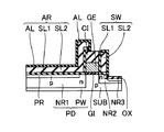
- the configuration of the antireflection film AR, the sidewall SW, and the like in the solid-state imaging device of the present embodiment formed by the above manufacturing method will be described.
- the colors of light captured by each of pixel 1 and pixel 2 are different from each other.
- the pn junction between the n-type region NR1 and the p-type well region PW in the region S in the semiconductor substrate SUB is a portion that functions as the photodiode PD.
- An antireflection film AR is formed on each of the photodiodes PD.
- the antireflection film AR has a three-layer structure in which a lower insulating film SL1, an upper insulating film SL2, and an upper antireflection film AL are stacked.
- the antireflection film AR of the pixel 1 and the antireflection film AR of the pixel 2 have different structures (film thickness, film quality, etc.).
- the thickness T1 of the antireflection film AR of the pixel 1 is thicker than the thickness T2 of the antireflection film AR of the pixel 2.
- the lower insulating films SL1 of the pixels 1 and 2 have the same thickness
- the upper antireflection films AL of the pixels 1 and 2 have the same thickness.
- the upper insulating film SL2 of the pixel 1 is thicker than the upper insulating film SL2 of the pixel 2.
- the antireflection film AR of the pixel 1 and the antireflection film AR of the pixel 2 are not limited to the above structure as long as they have different structures (film thickness, film quality, etc.).
- the thickness of the antireflection film AR in at least one pixel is larger than the width of the sidewall SW.
- the thickness T1 of the antireflection film AR of the pixel 1 is larger than the width W of the sidewall SW of the MOS transistor.
- the thickness T2 of the antireflection film AR of the pixel 2 may be thicker or thinner than the width W of the sidewall SW of the MOS transistor.
- the lower antireflection film SL is formed simultaneously with the sidewall SW by anisotropically etching the laminated films SL1 and SL2, the lower layer antireflection film SL has an end face ARE having a pattern generated by the anisotropic etching. Since the upper antireflection film AL is formed on the lower antireflection film SL after the anisotropic etching, the upper antireflection film AL is formed so as to cover the end surface ARE of the lower antireflection film SL.
- the MOS transistor includes a pair of source / drain regions NR3 formed on the surface of the semiconductor substrate SUB and spaced apart from each other, and an LDD region NR2 formed around each of the pair of source / drain regions NR3. And a gate electrode layer GE formed through a gate insulating film GI on a region sandwiched between the pair of source / drain regions NR3.
- a side wall SW is formed so as to cover the side wall of the gate electrode layer GE.
- the sidewall SW has a configuration in which two layers of a lower insulating film SL1 and an upper insulating film SL2 are stacked.
- the lower insulating film SL1 has an L shape in the cross-sectional view of FIG. 11, and the upper insulating film SL2 is formed on the lower insulating film SL1.
- the insulating film AL is formed so as to cover at least the side wall of the sidewall SW.
- the thickness W of the sidewall SW is determined by the thickness of the laminated film SL, and the thicknesses T1 and T2 of the antireflection film AR are determined by the thicknesses of the lower antireflection film SL and the upper antireflection film AL. It is determined. For this reason, the width W of the sidewall SW and the thicknesses T1 and T2 of the antireflection film AR can be controlled independently. Thereby, even if the width W of the sidewall SW becomes smaller according to the scaling law, the thickness T1 of the antireflection film AR can be made equal to or larger than the width W of the sidewall SW, and it is easy to cope with miniaturization.
- the upper antireflection film AL is formed on the lower antireflection film SL. For this reason, there are fewer restrictions on the antireflection film AR than when the antireflection film AR and the sidewall SW are formed in the same process.
- the upper antireflection film AL is formed, and at least one of the lower antireflection film SL and the upper antireflection film AL is removed. Is done. Therefore, it is possible to make the antireflection film AR with different thicknesses in each of the plurality of pixels PX without affecting the width W of the sidewall SW. Therefore, the antireflection effect can be optimized for each pixel PX.
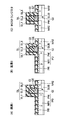
- the manufacturing method of both the pixel 1 and the pixel 2 first undergoes the same steps as those of the pixels 1 and 2 shown in FIGS. 3 (B) to 11 (B).
- the manufacturing method of the MOS transistor of this embodiment first, the same steps as those of the MOS transistor shown in FIGS. 3C to 11C are performed.
- a photoresist pattern PR6 is formed on the surface of the semiconductor substrate SUB by a normal photolithography technique.
- the photoresist pattern PR6 is formed so as to cover the photodiode PD of the pixel 1 and to open the photodiode PD and the MOS transistor of the pixel 2.
- the upper antireflection film AL of the pixel 2 is subjected to anisotropic etching. Thereby, the thickness of the antireflection film AR of the pixel 2 is controlled to be thinner than the thickness of the antireflection film AR of the pixel 1. Note that the pixel 1 in FIG.
- FIG. 12A shows a case where the end of the photoresist pattern PR6 is on the gate electrode GE, but in this case, the gate is effectively increased.
- the contact interlayer film is thin in order to prevent vignetting, and therefore, it is preferable that the gate is also low. May be.
- the pixel 2 in FIG. 12B is also the same. In this case, the photoresist pattern PR6 may not be provided.
- the above etching is performed, for example, so as to remove the entire thickness of the upper antireflection film AL.
- the etching may be performed so as to remove only a part of the thickness of the upper antireflection film AL, or after removing all the thickness of the upper antireflection film AL, It may be performed so as to remove only the part.
- the upper antireflection film AL remains only on the side wall of the sidewall SW except for the portion covered with the photoresist pattern PR6.
- photoresist pattern PR6 is removed by, for example, ashing.
- an interlayer insulating film II is formed on the entire surface of the semiconductor substrate SUB so as to cover the photodiode PD and the MOS transistor.
- the interlayer insulating film II is formed of, for example, a silicon oxide film using TEOS as a raw material, and has a flat upper surface by performing a planarization process such as CMP (Chemical-Mechanical-Polishing).
- contact hole CH that reaches source / drain region NR3 through interlayer insulating film II and insulating film OX is formed in interlayer insulating film II by a normal photolithography technique and etching technique. .
- a contact plug PL made of, for example, tungsten is formed so as to fill the contact hole CH.
- a wiring layer IL made of, for example, aluminum or copper is formed on interlayer insulating film II so as to be electrically connected to source / drain region NR3 through contact plug PL.
- interlayer insulating film II2 is formed on interlayer insulating film II so as to cover wiring layer IL.
- a high refractive index film HRL for lenses is formed on the interlayer insulating film II2.
- the high refractive index film HRL is processed.
- the lens LE is formed from the high refractive index film HRL by processing the high refractive index film HRL. Thereby, the solid-state imaging device of the present embodiment is manufactured.
- the thickness of antireflection film AR of pixel 1 is thicker than the thickness of antireflection film AR of pixel 2.
- the antireflection film AR of the pixel 1 has a three-layer structure in which a lower insulating film SL1, an upper insulating film SL2, and an upper antireflection film AL are stacked.
- the antireflection film AR of the pixel 2 has a two-layer structure in which a lower insulating film SL1 and an upper insulating film SL2 are stacked.
- the antireflection film AR of the pixel 2 may have a single layer structure of the lower insulating film SL1, or three layers in which the lower insulating film SL1, the upper insulating film SL2, and the upper antireflection film AL are stacked.
- the upper antireflection film AL may be thinner than the upper antireflection film AL of the pixel 1.
- the thickness of the antireflection film AR in at least one pixel is larger than the width of the sidewall SW.
- the antireflection film AR of the pixel 1 is thicker than the width W of the sidewall SW of the MOS transistor.
- the thickness T2 of the antireflection film AR of the pixel 2 may be thicker or thinner than the width W of the sidewall SW of the MOS transistor.
- an interlayer insulating film II made of, for example, a silicon oxide film is formed on the surface of the semiconductor substrate SUB so as to cover the photodiode PD and the MOS transistor.
- a contact hole CH reaching the source / drain region NR3 is formed in the interlayer insulating film II and the insulating film OX.
- a contact plug PL made of, for example, tungsten is formed so as to fill the contact hole CH.
- a wiring layer IL made of, for example, aluminum or copper is formed so as to be electrically connected to the source / drain region NR3 through the contact plug PL.
- An interlayer insulating film II2 made of, for example, a silicon oxide film is formed on the interlayer insulating film II so as to cover the wiring layer IL.
- a lens LE made of a high refractive index film HRL is formed on the interlayer insulating film II. The lens LE is for condensing light and irradiating the photodiode PD.
- the configuration of the first embodiment shown in FIG. 11 is the same as the configuration of the present embodiment shown in FIG. 19.
- the additional upper antireflection film AL is formed after the sidewalls are formed in a plurality of pixels, the same effects as those of the first embodiment can be obtained.
- the thickness of the lower antireflection film SL since not only the thickness of the lower antireflection film SL but also the thickness of the upper antireflection film AL can be controlled in the pixel 2, it is further easier to optimize the antireflection effect for each pixel. .
- a solid-state imaging device having an R pixel (first pixel), a G pixel (second pixel), and a B pixel (third pixel) as a plurality of pixels and having a MOS transistor will be described.
- a method for manufacturing the solid-state imaging device according to the present embodiment will be described mainly with reference to FIGS.
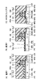
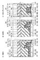
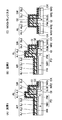
- Each of the R pixels shown in (A) of FIGS. 20 to 23 corresponds to a cross section taken along the line IIIA-IIIA of FIG. 1, for example, and each of the G pixels shown in (B) of FIGS. Corresponds to the cross section taken along the line IIIB-IIIB. 20 to 23 corresponds to the cross section taken along the line XXC-XXC in FIG. 1, for example, and the MOS transistor shown in each of FIGS. 20 to 23 in FIG. 1 corresponds to a cross section taken along line IIIC-IIIC.
- the manufacturing method of the R pixel in this embodiment first, the same process as that of the pixel 1 shown in FIGS. 3 (A) to 10 (A) is performed. Further, the manufacturing method of both the G pixel and the B pixel goes through the same steps as those of the pixel 2 shown in FIGS. 3 (B) to 10 (B). The manufacturing method of the MOS transistor according to the present embodiment undergoes the same steps as those of the MOS transistor shown in FIGS. 3 (C) to 10 (C).
- FIG. 20 shows a state after the steps so far.
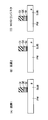
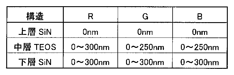
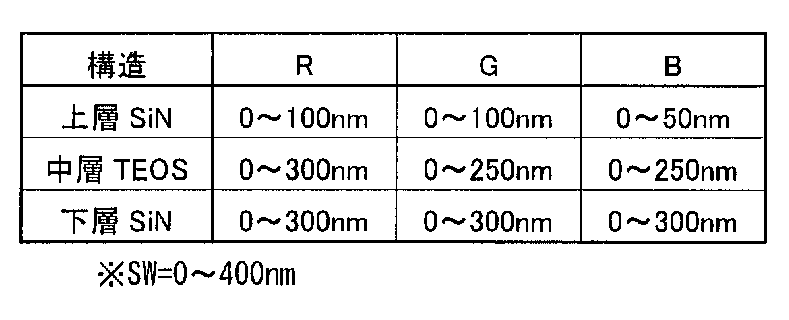
- Table 1 below shows the thickness of the lower insulating film SL1 and the thickness of the upper insulating film SL2 formed in each of the R pixel, the G pixel, and the B pixel in the process of FIG.
- the lower insulating film SL1 is marked as “lower SiN”, for example, as a silicon nitride film
- the upper insulating film SL2 is a silicon oxide film formed, for example, using TEOS (Tetra Ethyl Ortho Silicate) as a raw material.
- TEOS Tetra Ethyl Ortho Silicate
- the sum of the film thicknesses of the lower layer SiN and the middle layer TEOS shown in Table 1 is set to be the same as the width of the sidewall SW.
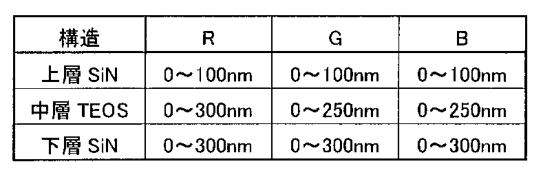
- the thickness of the “upper layer SiN” is shown in Table 2 below.
- an insulating film AL constituting an upper antireflection film is formed on the entire surface of semiconductor substrate SUB.
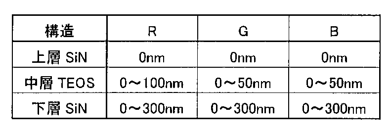
- This insulating film AL is formed of, for example, a silicon nitride film having a thickness of 0 to 100 nm. Table 3 below shows the thicknesses of “lower layer SiN”, “middle layer TEOS”, and “upper layer SiN” formed in each of the R pixel, G pixel, and B pixel in this state.
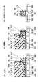
- a photoresist pattern PR6 is formed on the surface of semiconductor substrate SUB by a normal photolithography technique.
- the photoresist pattern PR6 is formed so as to cover the photodiode PD of the R pixel and the G pixel and to open the photodiode PD and the MOS transistor of the B pixel.
- the upper antireflection film AL of the B pixel is subjected to anisotropic etching. As a result, the upper antireflection film AL is removed and the thickness is reduced in the B pixel.
- This etching may be performed so that a part of the film thickness of the upper antireflection film AL in the B pixel remains, and after the upper antireflection film AL is completely removed, the thickness of the lower antireflection film SL is reduced. May be performed as described.
- the end of the photoresist pattern PR6 is on the gate electrode GE, but in this case, the gate is effectively increased.
- the contact interlayer film is thin in order to prevent vignetting, and therefore, it is preferable that the gate is also low. May be. The same applies to the B pixel in FIG. 22C. In this case, the photoresist pattern PR6 may be omitted.
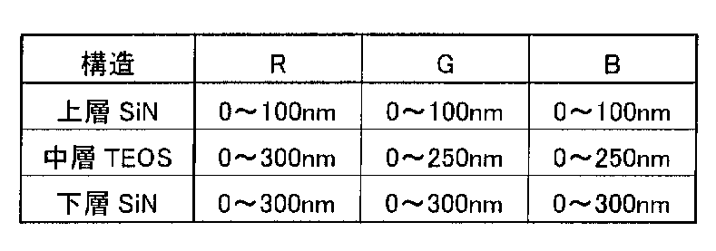
- Table 4 below shows the thicknesses of “lower layer SiN”, “middle layer TEOS”, and “upper layer SiN” formed in each of the R pixel, G pixel, and B pixel in this state.
- the photoresist pattern PR6 (FIG. 22) is removed by, for example, ashing to obtain the structure shown in FIG.
- the solid-state imaging device of the present embodiment is formed through substantially the same steps as those of the second embodiment shown in FIGS.
- the additional upper antireflection film AL is formed after the sidewall SW is formed in the plurality of pixels PX, the same effects as those of the first embodiment can be obtained. Further, the sidewall SW common to all the MOS transistors can be formed, and the antireflection film AR optimized for each of the R pixel, the G pixel, and the B pixel can be realized by a relatively simple process.
- the thickness of the antireflection film formed on each of the R pixel, G pixel, and B pixel is optimal. It is conceivable that the value also has a relationship of red light> green light> blue light.
- an antireflection film is formed so as to satisfy the above film thickness relationship.
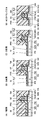
- Each of the R pixels shown in (A) of FIGS. 24 to 28 corresponds to, for example, a cross section taken along the line IIIA-IIIA of FIG. 1, and each of the G pixels shown in (B) of FIGS. Corresponds to the cross section taken along the line IIIB-IIIB.
- Each of the B pixels shown in (C) of FIGS. 24 to 28 corresponds to, for example, a cross section taken along line XXC-XXC of FIG. 1, and each of the MOS transistors shown in (D) of FIGS. 1 corresponds to a cross section taken along line IIIC-IIIC.
- the manufacturing method of the R pixel, the G pixel, the B pixel, and the MOS transistor in the present embodiment first undergoes the same steps as those shown in FIGS. A state after the steps up to here is shown in FIG.
- Table 5 below shows the thickness of the lower insulating film SL1 and the thickness of the upper insulating film SL2 formed in each of the R pixel, the G pixel, and the B pixel in the process of FIG.
- the title of “lower layer SiN” in Table 5 is the same as the title of “lower layer SiN” in Tables 1 to 4.
- the thickness of “middle layer TEOS” in Table 5 means the total thickness of the upper insulating film SL2 of the lower antireflection film SL and the lower insulating film AL1 of the upper antireflection film AL.
- the thickness of “upper layer SiN” in Table 5 means the thickness of the upper insulating film AL2 of the upper antireflection film AL.
- the thickness of the “middle layer TEOS” in Table 5 is only the thickness of the upper insulating film SL2 of the lower antireflection film SL.
- photoresist pattern PR5 is formed on the surface of semiconductor substrate SUB by a normal photoengraving technique.
- the photoresist pattern PR5 is formed so as to cover the photodiode PD of the R pixel and the MOS transistor and to open the photodiode PD of the G pixel and the B pixel.
- anisotropic etching is performed on the lower antireflection film SL of the G pixel and the B pixel. Thereby, a part of the thickness of the lower antireflection film SL is removed in the G pixel and the B pixel, and the thickness is reduced.
- photoresist pattern PR5 is removed by, for example, ashing.
- an insulating film AL constituting the upper antireflection film is formed on the entire surface of the semiconductor substrate SUB.
- This insulating film AL is formed of a laminated film of a lower insulating film AL1 and an upper insulating film AL2.
- Lower insulating film AL1 is a silicon oxide film having a thickness of 0 to 200 nm, for example
- upper insulating film AL2 is a silicon nitride film having a thickness of 0 to 100 nm, for example.
- Table 7 below shows the thicknesses of the “lower layer SiN”, “middle layer TEOS”, and “upper layer SiN” formed in each of the R pixel, the G pixel, and the B pixel in this state.
- a photoresist pattern PR6 is formed on the surface of semiconductor substrate SUB by a normal photolithography technique.
- the photoresist pattern PR6 is formed so as to cover the photodiode PD of the R pixel and the G pixel and to open the photodiode PD and the MOS transistor of the B pixel.
- the upper antireflection film AL of the B pixel is subjected to anisotropic etching.
- the upper insulating film AL2 is removed and the thickness is reduced in the B pixel.
- This etching may be performed so that a part of the thickness of the upper insulating film AL2 in the B pixel remains, and the thickness of the lower insulating film AL1 is reduced after the upper insulating film AL2 is completely removed. It may be done.
- the end of the photoresist pattern PR6 is on the gate electrode GE.
- the gate is effectively increased.
- the contact interlayer film is thin in order to prevent vignetting, and therefore, it is preferable that the gate is also low. May be.
- the photoresist pattern PR6 may be omitted.
- Table 8 below shows the thicknesses of the “lower layer SiN”, “middle layer TEOS”, and “upper layer SiN” formed in each of the R pixel, G pixel, and B pixel in this state.
- the photoresist pattern PR6 (FIG. 27) is removed by, for example, ashing to obtain the structure shown in FIG.
- the solid-state imaging device of the present embodiment is formed through substantially the same steps as those of the second embodiment shown in FIGS.
- the additional upper antireflection film AL is formed after the sidewall SW is formed in the plurality of pixels PX, the same effects as those of the first embodiment can be obtained. Further, the sidewall SW common to all the MOS transistors can be formed, and the antireflection film AR optimized for each of the R pixel, the G pixel, and the B pixel can be realized by a relatively simple process.
- the method for forming the borderless active layer contact according to the present embodiment undergoes the steps shown in FIGS. 3 to 11, for example. Thereafter, referring to FIG. 29, a photoresist pattern PR6 is formed on the surface of semiconductor substrate SUB by a normal photolithography technique.
- the photoresist pattern PR6 is formed so as to cover the photodiode PD and the MOS transistor of the pixel 1 and to open the photodiode PD of the pixel 2.
- the upper antireflection film AL of the pixel 2 is subjected to anisotropic etching.
- the thickness of the antireflection film AR of the pixel 2 is controlled to be thinner than the thickness of the antireflection film AR of the pixel 1.
- the insulating film AL for example, silicon nitride film
- photoresist pattern PR6 is removed by, for example, ashing.
- an interlayer insulating film II is formed so as to cover the photodiode PD and the MOS transistor.
- the interlayer insulating film II is formed of, for example, a silicon oxide film using TEOS as a raw material, and has a flat upper surface by performing a flattening process such as CMP.
- anisotropic etching is performed on interlayer insulating film II until the surface of insulating film AL is exposed by a normal photolithography technique and etching technique.
- etching conditions are selected such that the insulating film AL is not removed as much as possible by etching.
- a contact hole CH exposing the surface of the insulating film AL is formed in the interlayer insulating film II.
- the insulating film AL exposed from the contact hole CH is etched, and the underlying insulating film OX is exposed.
- the etching performed on the insulating film AL is performed under etching conditions different from the etching for removing the interlayer insulating film.
- the exposed insulating film OX is further removed by etching, so that the source / drain region NR3 is exposed from the contact hole CH.
- a contact hole CH that reaches the source / drain region NR3 through the interlayer insulating film II, the insulating film AL, and the insulating film OX is formed.
- the contact hole CH is opened in the interlayer insulating film II with the insulating film AL left so as to cover the upper and side portions of the sidewall SW.
- This stopper insulating film AL is made of, for example, a silicon nitride film, and the etching selectivity can be set high with respect to the interlayer insulating film II made of a silicon oxide film. Therefore, at the time of etching for forming the contact hole CH, the stopper insulating film AL functions as an etching stopper film.
- the thickness of the insulating film AL is smaller than the thickness of the interlayer insulating film II, it is possible to suppress the side walls SW and the like under the insulating film AL from being scraped. Can do.
- the contact hole CH reaching the source / drain region NR3 can be formed while suppressing the side wall SW from being scraped.
- the stopper insulating film AL as an etching stopper, it is possible to suppress the side wall SW from being scraped, and it becomes easy to cope with miniaturization.
- the laminated film SL may have a three-layer structure as in the present embodiment shown in FIG.
- the laminated film SL has a configuration in which a lower insulating film SL1, an intermediate insulating film SL2, and an upper insulating film SL3 are laminated.
- Lower insulating film SL1 is, for example, a silicon nitride film
- middle insulating film SL2 is, for example, a silicon oxide film formed using TEOS as a raw material
- upper insulating film SL3 is, for example, a silicon nitride film.
- the laminated film SL may have a laminated structure of four or more layers.
- the insulating film AL constituting the upper antireflection film has a single layer structure.
- the insulating film AL to be formed may have a two-layer structure.
- This insulating film AL has a lower insulating film AL1 and an upper insulating film AL2.
- Lower insulating film AL1 is, for example, a silicon oxide film
- upper insulating film AL2 is, for example, a silicon nitride film.
- the insulating film AL in the first to fifth embodiments may have a laminated structure of three or more layers.
- Insulating film AL constituting the upper antireflection film in the above first to fifth embodiments may be formed so as not to be deposited on semiconductor substrate SUB and gate electrode layer GE by selective growth as shown in FIG. Good. According to this method, since the etching process of the upper antireflection film can be omitted, damage to the MOS transistor by the etching process can be reduced.
- this transistor may be a MIS (Metal Insulator Semiconductor) transistor whose gate insulating film is made of an insulating film other than a silicon oxide film. Any type field effect transistor may be used. Although the n-channel MOS transistor has been described, the transistor may be a p-channel MOS transistor.
- the conductivity type between the semiconductor substrate SUB and the well is arbitrary.
- the photodiode PD has been described, the present invention can be applied to any device capable of photoelectric conversion.
- AL insulating film (upper antireflection film), AL1 lower insulating film, AL2 upper insulating film, AR antireflection film, ARS1, ARS2 end face, ATR amplifying transistor, CH contact hole, CI cap insulating film, GE gate electrode layer, GI Gate insulating film, HRL high refractive index film HRL, II, II2 interlayer insulating film, IL wiring layer, LE lens, NR1, NR3 n-type region, NR2 n-type LDD region, PD photodiode, PL contact plug, PR p + region PR1, PR1A, PR2, PR3, PR4, PR5, PR6 Photoresist pattern, PS vertical signal line, PW p-type well region, PWS power supply line, PX pixel, RTR reset transistor, SL laminated film (lower antireflection film) , SL1 Lower insulation film, SL2 Upper insulation film (intermediate insulation film), SL3 Upper insulation film Edge film, SS selection signal line, STR
Landscapes
- Solid State Image Pick-Up Elements (AREA)
- Transforming Light Signals Into Electric Signals (AREA)
Abstract
Description
(実施の形態1)
まず本実施の形態における固体撮像装置の構成について説明する。
次に、上記の製造方法により形成される本実施の形態の固体撮像装置における反射防止膜AR、サイドウォールSWなどの構成について説明する。
本実施の形態によれば、積層膜SLの厚さでサイドウォールSWの幅Wが決定され、下層反射防止膜SLと上層反射防止膜ALとの厚みで反射防止膜ARの厚みT1、T2が決定される。このため、サイドウォールSWの幅Wと反射防止膜ARの厚みT1、T2とを独立して制御することができる。これにより、サイドウォールSWの幅Wがスケーリング則に従って小さくなっても、反射防止膜ARの厚みT1をサイドウォールSWの幅W以上にすることができ、微細化に対応することが容易である。
上記の実施の形態1においては、画素1および画素2の各々の反射防止膜ARの厚みを変えるために、下層反射防止膜SLをエッチングする方法について説明したが、上層反射防止膜ALをエッチングすることにより画素1および画素2の各々の反射防止膜ARの厚みが変えられてもよい。
本実施の形態においては、複数の画素としてR画素(第1画素)、G画素(第2画素)およびB画素(第3画素)を有し、かつMOSトランジスタを有する固体撮像装置について説明する。まず本実施の形態の固体撮像装置の製造方法について主に図20~図23を用いて説明する。


本実施の形態においては、実施の形態3と同様、複数の画素としてR画素(第1画素)、G画素(第2画素)およびB画素(第3画素)を有し、かつMOSトランジスタを有する固体撮像装置について説明する。まず本実施の形態の固体撮像装置の製造方法について主に図24~図28を用いて説明する。

本実施の形態においては、上層反射防止膜を構成する絶縁膜ALをエッチングストッパ膜として使用してボーダレス活性層コンタクトを形成する方法について主に図29~図32を用いて説明する。
上記の実施の形態1~5においては積層膜SLが2層構造の場合について説明したが、図33に示す本実施の形態のように積層膜SLは3層構造であってもよい。この積層膜SLは、下層絶縁膜SL1と、中層絶縁膜SL2と、上層絶縁膜SL3とが積層された構成を有している。下層絶縁膜SL1はたとえばシリコン窒化膜であり、中層絶縁膜SL2はたとえばTEOSを原料として形成されたシリコン酸化膜であり、上層絶縁膜SL3はたとえばシリコン窒化膜である。また積層膜SLは4層以上の積層構造であってもよい。
上記の実施の形態1~3および5においては上層反射防止膜を構成する絶縁膜ALが単層構造の場合について説明したが、図34に示す本実施の形態のように上層反射防止膜を構成する絶縁膜ALは2層構造であってもよい。この絶縁膜ALは、下層絶縁膜AL1と上層絶縁膜AL2とを有している。下層絶縁膜AL1はたとえばシリコン酸化膜であり、上層絶縁膜AL2はたとえばシリコン窒化膜である。また実施の形態1~5の絶縁膜ALは3層以上の積層構造であってもよい。
上記の実施の形態1~5における上層反射防止膜を構成する絶縁膜ALは、図35に示すように選択成長により、半導体基板SUB上およびゲート電極層GE上に堆積しないように形成されてもよい。この方法によれば、上層反射防止膜のエッチング工程を省略することができるため、エッチング工程がMOSトランジスタに与えるダメージを軽減することができる。
Claims (14)
- 複数の画素(PX)を構成する複数の光電変換部(PD)と、絶縁ゲート型電界効果トランジスタ部と、それぞれが複数の前記光電変換部の各々の上に形成された複数の第1の膜(AR)とを含む固体撮像装置の製造方法であって、
複数の前記光電変換部上と前記絶縁ゲート型電界効果トランジスタ部のゲート電極層(GE)上とを覆うように、複数の絶縁膜よりなる積層膜(SL)を形成する工程と、
前記積層膜に選択的に異方性エッチングを施すことにより、複数の前記光電変換部の各々の上に前記積層膜を残して下層膜(SL)を形成するとともに、前記ゲート電極層の側壁に前記積層膜を残して側壁絶縁膜(SW)を形成する工程と、
前記ゲート電極層および前記側壁絶縁膜に覆われていない領域に不純物を導入して、前記絶縁ゲート型電界効果トランジスタのソース/ドレイン領域(NR3)を形成する工程と、
前記不純物の導入後に少なくとも前記下層膜の上に上層膜(AL)を形成する工程と、
複数の前記光電変換部のうち少なくとも2つの光電変換部上のそれぞれの前記第1の膜の厚みが互いに異なる厚みとなるように、前記上層膜および前記下層膜の少なくともいずれかをエッチングする工程とを備えた、固体撮像装置の製造方法。 - 前記上層膜(AL)および前記下層膜(SL)の少なくともいずれかをエッチングする前記工程は、前記側壁絶縁膜(SW)の形成後であって前記上層膜の形成前に前記下層膜をエッチングする工程を含む、請求の範囲第1項に記載の固体撮像装置の製造方法。
- 前記上層膜(AL)および前記下層膜(SL)の少なくともいずれかをエッチングする前記工程は、前記上層膜の形成後に少なくとも前記上層膜をエッチングする工程を含む、請求の範囲第1項に記載の固体撮像装置の製造方法。
- 前記上層膜(AL)および前記下層膜(SL)の少なくともいずれかをエッチングする前記工程は、前記上層膜をエッチングして前記下層膜を露出させた後に、露出した前記下層膜をエッチングする工程を含む、請求の範囲第3項に記載の固体撮像装置の製造方法。
- 前記複数の画素(PX)は、互いに異なる色の光を撮像する第1画素、第2画素および第3画素を含み、
前記上層膜(AL)および前記下層膜(SL)の少なくともいずれかをエッチングする前記工程は、
前記第1画素の前記光電変換部(PD)上の前記下層膜を残しつつ、前記第2画素および前記第3画素の双方の前記光電変換部上の前記下層膜を前記側壁絶縁膜の形成後であって前記上層膜の形成前にエッチングする工程と、
前記第3画素の前記光電変換部上の前記上層膜を前記上層膜の形成後にエッチングする工程とを含む、請求の範囲第1項に記載の固体撮像装置の製造方法。 - 前記上層膜(AL)および前記下層膜(SL)の少なくともいずれかをエッチングする前記工程は、前記第3画素の前記上層膜をエッチングして前記下層膜を露出させた後に、露出した前記下層反射防止膜をエッチングする工程を含む、請求の範囲第5項に記載の固体撮像装置の製造方法。
- 前記積層膜(SL)は3層以上の絶縁膜より形成される、請求の範囲第1項に記載の固体撮像装置の製造方法。
- 前記上層膜(AL)はシリコン窒化膜単層により形成される、請求の範囲第1項に記載の固体撮像装置の製造方法。
- 前記上層膜(AL)は2層以上の膜により形成される、請求の範囲第1項に記載の固体撮像装置の製造方法。
- 前記上層膜(AL)はシリコン酸化膜とシリコン窒化膜とが積層されて形成される、請求の範囲第9項に記載の固体撮像装置の製造方法。
- 前記上層膜(AL)は選択成長により形成される、請求の範囲第1項に記載の固体撮像装置の製造方法。
- 前記上層膜(AL)を形成する前記工程は、前記上層膜を前記ゲート電極層(GE)上および前記側壁絶縁膜(SW)上を覆うように形成する工程を含み、
前記第1の膜(AR)の形成後に、前記上層膜とは異なる材質よりなる層間絶縁膜(II)を前記ソース/ドレイン領域(NR3)上および前記第1の絶縁膜上を覆うように形成する工程と、
前記層間絶縁膜を第1の条件でエッチングすることにより、前記層間絶縁膜に前記上層膜の一部を露出するコンタクトホールを形成する工程と、
前記第1の条件とは異なる第2の条件で前記上層膜をエッチングすることにより、前記コンタクトホールから露出する前記上層膜を除去する工程とをさらに備えた、請求の範囲第1項に記載の固体撮像装置の製造方法。 - 互いに異なる色の光を撮像するための第1画素(PX)および第2画素(PX)を有する固体撮像装置であって、
前記第1画素に対応する第1の光電変換部(PD)と、
前記第2画素に対応する第2の光電変換部(PD)と、
ゲート電極層(GE)を有する絶縁ゲート型電界効果トランジスタ部と、
それぞれが前記第1および第2の光電変換部の各々の上に形成された2つの第1の膜(AR)と、
前記ゲート電極層の側壁に形成された側壁絶縁膜(SW)とを備え、
前記第1の光電変換部上に形成された前記第1の膜と前記第2の光電変換部上に形成された前記第1の膜は、互いに異なる構造を有し、
前記第1の光電変換部上に形成された前記第1の膜は、下層膜(SL)と、前記下層膜上に位置しかつ前記下層膜のパターンの端面(ARE)を覆う上層膜(AL)とを含み、
前記側壁絶縁膜は前記下層膜から成る、固体撮像装置。 - 前記第1の光電変換部上に形成された前記第1の膜の厚みは、前記側壁絶縁膜の幅よりも厚い、請求の範囲第13項記載の固体撮像装置。
Priority Applications (8)
| Application Number | Priority Date | Filing Date | Title |
|---|---|---|---|
| JP2011510129A JP5343124B2 (ja) | 2009-04-24 | 2009-04-24 | 固体撮像装置およびその製造方法 |
| PCT/JP2009/058127 WO2010122657A1 (ja) | 2009-04-24 | 2009-04-24 | 固体撮像装置およびその製造方法 |
| US13/265,513 US8728853B2 (en) | 2009-04-24 | 2009-04-24 | Solid-state image sensing device and method of manufacturing the same |
| TW099108135A TWI493698B (zh) | 2009-04-24 | 2010-03-19 | Solid state image pickup apparatus and manufacturing method thereof |
| US14/257,746 US9064771B2 (en) | 2009-04-24 | 2014-04-21 | Solid-state image sensing device and method of manufacturing the same |
| US14/713,866 US9281329B2 (en) | 2009-04-24 | 2015-05-15 | Solid-state image sensing device and method of manufacturing the same |
| US15/017,950 US9583532B2 (en) | 2009-04-24 | 2016-02-08 | Solid-state image sensing device and method of manufacturing the same |
| US15/409,880 US10157955B2 (en) | 2009-04-24 | 2017-01-19 | Solid-state image sensing device and method of manufacturing the same |
Applications Claiming Priority (1)
| Application Number | Priority Date | Filing Date | Title |
|---|---|---|---|
| PCT/JP2009/058127 WO2010122657A1 (ja) | 2009-04-24 | 2009-04-24 | 固体撮像装置およびその製造方法 |
Related Child Applications (2)
| Application Number | Title | Priority Date | Filing Date |
|---|---|---|---|
| US13/265,513 A-371-Of-International US8728853B2 (en) | 2009-04-24 | 2009-04-24 | Solid-state image sensing device and method of manufacturing the same |
| US14/257,746 Division US9064771B2 (en) | 2009-04-24 | 2014-04-21 | Solid-state image sensing device and method of manufacturing the same |
Publications (1)
| Publication Number | Publication Date |
|---|---|
| WO2010122657A1 true WO2010122657A1 (ja) | 2010-10-28 |
Family
ID=43010793
Family Applications (1)
| Application Number | Title | Priority Date | Filing Date |
|---|---|---|---|
| PCT/JP2009/058127 Ceased WO2010122657A1 (ja) | 2009-04-24 | 2009-04-24 | 固体撮像装置およびその製造方法 |
Country Status (4)
| Country | Link |
|---|---|
| US (5) | US8728853B2 (ja) |
| JP (1) | JP5343124B2 (ja) |
| TW (1) | TWI493698B (ja) |
| WO (1) | WO2010122657A1 (ja) |
Cited By (6)
| Publication number | Priority date | Publication date | Assignee | Title |
|---|---|---|---|---|
| JP2013051317A (ja) * | 2011-08-31 | 2013-03-14 | Renesas Electronics Corp | 半導体装置の製造方法 |
| JP2013084741A (ja) * | 2011-10-07 | 2013-05-09 | Canon Inc | 光電変換装置および撮像システム |
| JP2015012175A (ja) * | 2013-06-28 | 2015-01-19 | キヤノン株式会社 | 光電変換装置の製造方法、光電変換装置、及び撮像システム |
| KR20160021440A (ko) * | 2013-06-14 | 2016-02-25 | 르네사스 일렉트로닉스 가부시키가이샤 | 촬상 장치의 제조 방법 및 촬상 장치 |
| JP2018101804A (ja) * | 2018-03-08 | 2018-06-28 | ルネサスエレクトロニクス株式会社 | 撮像装置の製造方法および撮像装置 |
| WO2023074215A1 (ja) * | 2021-10-28 | 2023-05-04 | ソニーセミコンダクタソリューションズ株式会社 | 半導体装置及び撮像装置 |
Families Citing this family (5)
| Publication number | Priority date | Publication date | Assignee | Title |
|---|---|---|---|---|
| JP3371142B2 (ja) | 1991-09-27 | 2003-01-27 | 日本フエロー株式会社 | 鋼材の酸化脱炭防止用組成物 |
| US8754495B1 (en) * | 2013-04-26 | 2014-06-17 | Texas Instruments Incorporated | Photodetector array having different photodiode structures |
| CN104603949B (zh) * | 2014-01-27 | 2019-10-01 | 瑞萨电子株式会社 | 半导体器件 |
| US9893019B2 (en) * | 2015-09-15 | 2018-02-13 | Taiwan Semiconductor Manufacturing Co., Ltd. | Semiconductor structure, integrated circuit device, and method of forming semiconductor structure |
| JP2024046470A (ja) | 2022-09-22 | 2024-04-03 | 株式会社東芝 | 固体撮像装置 |
Citations (6)
| Publication number | Priority date | Publication date | Assignee | Title |
|---|---|---|---|---|
| JP2004023107A (ja) * | 2002-06-20 | 2004-01-22 | Samsung Electronics Co Ltd | イメージセンサ及びその製造方法 |
| JP2004228425A (ja) * | 2003-01-24 | 2004-08-12 | Renesas Technology Corp | Cmosイメージセンサの製造方法 |
| JP2005142510A (ja) * | 2003-11-10 | 2005-06-02 | Matsushita Electric Ind Co Ltd | 固体撮像装置およびその製造方法 |
| JP2006040986A (ja) * | 2004-07-23 | 2006-02-09 | Sony Corp | 固体撮像装置及びその製造方法 |
| JP2007055141A (ja) * | 2005-08-25 | 2007-03-08 | Fuji Xerox Co Ltd | フッ素樹脂被覆部材及びその製造方法、定着装置並びに画像形成装置 |
| JP2009026848A (ja) * | 2007-07-18 | 2009-02-05 | Panasonic Corp | 固体撮像素子及びその製造方法 |
Family Cites Families (10)
| Publication number | Priority date | Publication date | Assignee | Title |
|---|---|---|---|---|
| JP3103064B2 (ja) | 1998-04-23 | 2000-10-23 | 松下電子工業株式会社 | 固体撮像装置およびその製造方法 |
| JP2000196051A (ja) | 1998-12-25 | 2000-07-14 | Matsushita Electric Ind Co Ltd | 固体撮像素子およびその製造方法 |
| US7235835B2 (en) | 2002-05-14 | 2007-06-26 | Sony Corporation | Semiconductor device and its manufacturing method, and electronic device |
| KR100508086B1 (ko) * | 2002-09-11 | 2005-08-17 | 삼성전자주식회사 | 씨모스 이미지 센서 및 그 제조방법 |
| JP3840214B2 (ja) | 2003-01-06 | 2006-11-01 | キヤノン株式会社 | 光電変換装置及び光電変換装置の製造方法及び同光電変換装置を用いたカメラ |
| JP2004335588A (ja) | 2003-05-01 | 2004-11-25 | Renesas Technology Corp | 固体撮像装置及びその製造方法 |
| JP4695902B2 (ja) | 2005-03-18 | 2011-06-08 | キヤノン株式会社 | 固体撮像装置の製造方法 |
| KR100672730B1 (ko) * | 2005-07-15 | 2007-01-24 | 동부일렉트로닉스 주식회사 | 씨모스 이미지 센서 및 그 제조방법 |
| JP5082855B2 (ja) | 2005-11-11 | 2012-11-28 | 株式会社ニコン | 反射防止膜を有する固体撮像装置および表示装置並びにその製造方法 |
| JP2008041958A (ja) | 2006-08-07 | 2008-02-21 | Sharp Corp | 固体撮像装置およびその製造方法、電子情報機器 |
-
2009
- 2009-04-24 JP JP2011510129A patent/JP5343124B2/ja not_active Expired - Fee Related
- 2009-04-24 WO PCT/JP2009/058127 patent/WO2010122657A1/ja not_active Ceased
- 2009-04-24 US US13/265,513 patent/US8728853B2/en active Active
-
2010
- 2010-03-19 TW TW099108135A patent/TWI493698B/zh not_active IP Right Cessation
-
2014
- 2014-04-21 US US14/257,746 patent/US9064771B2/en active Active
-
2015
- 2015-05-15 US US14/713,866 patent/US9281329B2/en not_active Expired - Fee Related
-
2016
- 2016-02-08 US US15/017,950 patent/US9583532B2/en not_active Expired - Fee Related
-
2017
- 2017-01-19 US US15/409,880 patent/US10157955B2/en active Active
Patent Citations (6)
| Publication number | Priority date | Publication date | Assignee | Title |
|---|---|---|---|---|
| JP2004023107A (ja) * | 2002-06-20 | 2004-01-22 | Samsung Electronics Co Ltd | イメージセンサ及びその製造方法 |
| JP2004228425A (ja) * | 2003-01-24 | 2004-08-12 | Renesas Technology Corp | Cmosイメージセンサの製造方法 |
| JP2005142510A (ja) * | 2003-11-10 | 2005-06-02 | Matsushita Electric Ind Co Ltd | 固体撮像装置およびその製造方法 |
| JP2006040986A (ja) * | 2004-07-23 | 2006-02-09 | Sony Corp | 固体撮像装置及びその製造方法 |
| JP2007055141A (ja) * | 2005-08-25 | 2007-03-08 | Fuji Xerox Co Ltd | フッ素樹脂被覆部材及びその製造方法、定着装置並びに画像形成装置 |
| JP2009026848A (ja) * | 2007-07-18 | 2009-02-05 | Panasonic Corp | 固体撮像素子及びその製造方法 |
Cited By (10)
| Publication number | Priority date | Publication date | Assignee | Title |
|---|---|---|---|---|
| JP2013051317A (ja) * | 2011-08-31 | 2013-03-14 | Renesas Electronics Corp | 半導体装置の製造方法 |
| JP2013084741A (ja) * | 2011-10-07 | 2013-05-09 | Canon Inc | 光電変換装置および撮像システム |
| KR20160021440A (ko) * | 2013-06-14 | 2016-02-25 | 르네사스 일렉트로닉스 가부시키가이샤 | 촬상 장치의 제조 방법 및 촬상 장치 |
| JPWO2014199509A1 (ja) * | 2013-06-14 | 2017-02-23 | ルネサスエレクトロニクス株式会社 | 撮像装置の製造方法 |
| US9698187B2 (en) | 2013-06-14 | 2017-07-04 | Renesas Electronics Corporation | Method for manufacturing imaging apparatus, and imaging apparatus |
| US9887220B2 (en) | 2013-06-14 | 2018-02-06 | Renesas Elctronics Corporation | Method for manufacturing imaging apparatus, and imaging apparatus |
| KR102120666B1 (ko) * | 2013-06-14 | 2020-06-09 | 르네사스 일렉트로닉스 가부시키가이샤 | 촬상 장치의 제조 방법 및 촬상 장치 |
| JP2015012175A (ja) * | 2013-06-28 | 2015-01-19 | キヤノン株式会社 | 光電変換装置の製造方法、光電変換装置、及び撮像システム |
| JP2018101804A (ja) * | 2018-03-08 | 2018-06-28 | ルネサスエレクトロニクス株式会社 | 撮像装置の製造方法および撮像装置 |
| WO2023074215A1 (ja) * | 2021-10-28 | 2023-05-04 | ソニーセミコンダクタソリューションズ株式会社 | 半導体装置及び撮像装置 |
Also Published As
| Publication number | Publication date |
|---|---|
| TW201110334A (en) | 2011-03-16 |
| US8728853B2 (en) | 2014-05-20 |
| JPWO2010122657A1 (ja) | 2012-10-22 |
| US20150249103A1 (en) | 2015-09-03 |
| US20160155772A1 (en) | 2016-06-02 |
| US10157955B2 (en) | 2018-12-18 |
| TWI493698B (zh) | 2015-07-21 |
| US20170133430A1 (en) | 2017-05-11 |
| US20140225174A1 (en) | 2014-08-14 |
| JP5343124B2 (ja) | 2013-11-13 |
| US20120037968A1 (en) | 2012-02-16 |
| US9583532B2 (en) | 2017-02-28 |
| US9281329B2 (en) | 2016-03-08 |
| US9064771B2 (en) | 2015-06-23 |
Similar Documents
| Publication | Publication Date | Title |
|---|---|---|
| JP5343124B2 (ja) | 固体撮像装置およびその製造方法 | |
| JP5930650B2 (ja) | 半導体装置の製造方法 | |
| US10411061B2 (en) | Semiconductor structure and fabrication method thereof | |
| KR100708829B1 (ko) | 반도체 촬상 장치 | |
| CN102074563B (zh) | 具有增强的背面照明量子效率的图像传感器 | |
| JP5095287B2 (ja) | 固体撮像素子及びその製造方法 | |
| US20110062540A1 (en) | Solid-state image sensor and method of manufacturing the same | |
| US12068349B2 (en) | Method of manufacturing solid-state image sensor, solid-state image sensor, and camera | |
| JP6346488B2 (ja) | 半導体装置、固体撮像装置、それらの製造方法およびカメラ | |
| JP4486043B2 (ja) | Cmosイメージセンサー及びその製造方法 | |
| US7462520B2 (en) | Methods of fabricating an image sensor | |
| KR20100077986A (ko) | 이미지 센서 및 그의 제조 방법 | |
| WO2008018329A1 (en) | Solid-state imaging apparatus and method for manufacturing same, and electronic information apparatus | |
| JP5875368B2 (ja) | 半導体装置の製造方法 | |
| JP5442085B2 (ja) | 固体撮像素子 | |
| KR100741920B1 (ko) | 씨모스(cmos) 이미지 센서의 제조 방법 | |
| KR20100030812A (ko) | 씨모스 이미지 센서의 제조방법 | |
| JP2006012999A (ja) | 固体撮像装置の製造方法 | |
| KR20080011550A (ko) | 이미지 센서의 제조 방법 |
Legal Events
| Date | Code | Title | Description |
|---|---|---|---|
| 121 | Ep: the epo has been informed by wipo that ep was designated in this application |
Ref document number: 09843657 Country of ref document: EP Kind code of ref document: A1 |
|
| ENP | Entry into the national phase |
Ref document number: 2011510129 Country of ref document: JP Kind code of ref document: A |
|
| WWE | Wipo information: entry into national phase |
Ref document number: 13265513 Country of ref document: US |
|
| NENP | Non-entry into the national phase |
Ref country code: DE |
|
| 122 | Ep: pct application non-entry in european phase |
Ref document number: 09843657 Country of ref document: EP Kind code of ref document: A1 |