WO2010116746A1 - Cu-Al-Co系合金の電極・配線を具備した電子部品 - Google Patents
Cu-Al-Co系合金の電極・配線を具備した電子部品 Download PDFInfo
- Publication number
- WO2010116746A1 WO2010116746A1 PCT/JP2010/002573 JP2010002573W WO2010116746A1 WO 2010116746 A1 WO2010116746 A1 WO 2010116746A1 JP 2010002573 W JP2010002573 W JP 2010002573W WO 2010116746 A1 WO2010116746 A1 WO 2010116746A1
- Authority
- WO
- WIPO (PCT)
- Prior art keywords
- wiring
- electrode
- glass
- electronic component
- powder
- Prior art date
- Legal status (The legal status is an assumption and is not a legal conclusion. Google has not performed a legal analysis and makes no representation as to the accuracy of the status listed.)
- Ceased
Links
Images










Classifications
-
- C—CHEMISTRY; METALLURGY
- C22—METALLURGY; FERROUS OR NON-FERROUS ALLOYS; TREATMENT OF ALLOYS OR NON-FERROUS METALS
- C22C—ALLOYS
- C22C9/00—Alloys based on copper
- C22C9/01—Alloys based on copper with aluminium as the next major constituent
-
- C—CHEMISTRY; METALLURGY
- C22—METALLURGY; FERROUS OR NON-FERROUS ALLOYS; TREATMENT OF ALLOYS OR NON-FERROUS METALS
- C22C—ALLOYS
- C22C9/00—Alloys based on copper
- C22C9/06—Alloys based on copper with nickel or cobalt as the next major constituent
-
- H—ELECTRICITY
- H01—ELECTRIC ELEMENTS
- H01J—ELECTRIC DISCHARGE TUBES OR DISCHARGE LAMPS
- H01J1/00—Details of electrodes, of magnetic control means, of screens, or of the mounting or spacing thereof, common to two or more basic types of discharge tubes or lamps
- H01J1/02—Main electrodes
-
- H—ELECTRICITY
- H05—ELECTRIC TECHNIQUES NOT OTHERWISE PROVIDED FOR
- H05K—PRINTED CIRCUITS; CASINGS OR CONSTRUCTIONAL DETAILS OF ELECTRIC APPARATUS; MANUFACTURE OF ASSEMBLAGES OF ELECTRICAL COMPONENTS
- H05K1/00—Printed circuits
- H05K1/02—Details
- H05K1/09—Use of materials for the conductive, e.g. metallic pattern
- H05K1/092—Dispersed materials, e.g. conductive pastes or inks
-
- H—ELECTRICITY
- H10—SEMICONDUCTOR DEVICES; ELECTRIC SOLID-STATE DEVICES NOT OTHERWISE PROVIDED FOR
- H10F—INORGANIC SEMICONDUCTOR DEVICES SENSITIVE TO INFRARED RADIATION, LIGHT, ELECTROMAGNETIC RADIATION OF SHORTER WAVELENGTH OR CORPUSCULAR RADIATION
- H10F77/00—Constructional details of devices covered by this subclass
- H10F77/20—Electrodes
- H10F77/206—Electrodes for devices having potential barriers
- H10F77/211—Electrodes for devices having potential barriers for photovoltaic cells
-
- H—ELECTRICITY
- H01—ELECTRIC ELEMENTS
- H01J—ELECTRIC DISCHARGE TUBES OR DISCHARGE LAMPS
- H01J2211/00—Plasma display panels with alternate current induction of the discharge, e.g. AC-PDPs
- H01J2211/20—Constructional details
- H01J2211/22—Electrodes
- H01J2211/225—Material of electrodes
-
- Y—GENERAL TAGGING OF NEW TECHNOLOGICAL DEVELOPMENTS; GENERAL TAGGING OF CROSS-SECTIONAL TECHNOLOGIES SPANNING OVER SEVERAL SECTIONS OF THE IPC; TECHNICAL SUBJECTS COVERED BY FORMER USPC CROSS-REFERENCE ART COLLECTIONS [XRACs] AND DIGESTS
- Y02—TECHNOLOGIES OR APPLICATIONS FOR MITIGATION OR ADAPTATION AGAINST CLIMATE CHANGE
- Y02E—REDUCTION OF GREENHOUSE GAS [GHG] EMISSIONS, RELATED TO ENERGY GENERATION, TRANSMISSION OR DISTRIBUTION
- Y02E10/00—Energy generation through renewable energy sources
- Y02E10/50—Photovoltaic [PV] energy
Definitions
- the present invention relates to a copper-based electrode / wiring material capable of suppressing oxidation, and an electronic component using the same for an electrode / wiring / contact component.
- Patent Document 1 there is known an electronic component material that contains Cu as a main component, contains Mo in an amount of 0.1 to 3.0 wt%, and improves the weather resistance of the entire Cu by uniformly mixing Mo into the grain boundary of Cu.
- addition of Mo is essential, and together with Mo, one or more elements from the group consisting of Al, Au, Ag, Ti, Ni, Co, and Si are added in a total amount of 0.1 to 3.0 wt%. Attempts have been made to further improve the weather resistance than when Mo alone is added.
- a highly reliable Cu-based material is strongly desired from the viewpoint of cost reduction and migration resistance improvement.
- the electrode / wiring itself of the Cu-based material loses its conductivity due to oxidation or is Cu-based wiring due to a high-temperature manufacturing process involving an oxidizing atmosphere.
- the material is in contact with the glass dielectric, there is a problem that bubbles are generated in the glass or glass ceramic at the interface. This is because the conductive member made of pure Cu or Cu-based metal is oxidized during the manufacturing process by a method including a high-temperature heat treatment process at 200 ° C.
- the case where the Cu-based wiring material is in contact with the glass dielectric includes not only the case where the member in contact with the wiring is glass or glass ceramics but also the case where the wiring itself contains a glass component.
- the present invention has been made in view of the above-described problems, and an object thereof is to provide an electronic component using a Cu-based conductive member that can suppress oxidation even in a heat treatment in an oxidizing atmosphere and can suppress an increase in electrical resistance. Furthermore, in an electronic component having a structure in contact with glass or glass ceramics, an object is to provide an electronic component using a Cu-based conductive member capable of suppressing the generation of bubbles in the glass or glass ceramics and excellent in migration resistance. And
- the present invention uses a ternary alloy composed of three elements of Cu, Al, and Co as a Cu-based wiring material capable of preventing oxidation of the electrode / wiring in an electronic component having electrodes or wiring.
- a part or all of the electrode or wiring has a chemical composition in which Al content: 10 at% to 25 at%, Co content: 5 at% to 20 at%, and the balance is composed of Cu and inevitable impurities.
- it is a ternary alloy in which two phases of a Cu solid solution in which Al and Co are dissolved in Cu and a CoAl intermetallic compound coexist.
- the electrode or the wiring has a structure in contact with glass or a glass ceramic member.
- the inevitable impurities contained in the ternary alloy of the present invention mean an element brought from the alloy raw material in the alloy manufacturing process or an element mixed in the manufacturing process.
- the content of inevitable impurities is desirably 1 wt% or less.
- a form of wiring or electrode in contact with glass or glass ceramic member for example, a structure in which wiring or electrode is formed on the surface of glass or glass ceramic member, or the surface of wiring or electrode is covered with glass or glass ceramic member Or a structure in which wires or electrodes are provided in holes provided in a glass or glass ceramic member.
- the above-described alloy of the present invention can provide a Cu-based electrode / wiring / contact material that can not only suppress oxidation even in a heat treatment in an oxidizing atmosphere but also can suppress an increase in electrical resistance.
- the present invention also relates to a wiring material obtained by mixing at least a conductive metal material powder and a glass powder and firing the mixture, wherein the conductive metal component has an Al content of 10 at% to 25 at% and a Co content of 5 at. It is characterized by an electrode / wiring material composed of 20% by mass to 20 at% and the balance being Cu and inevitable impurities.
- the present invention it is possible to provide a Cu-based conductive member capable of suppressing oxidation even in a heat treatment in an oxidizing atmosphere and suppressing an increase in electrical resistance, and an electronic component using the Cu-based conductive member. it can.
- an electronic component having a wiring in contact with glass or a glass ceramic member it is possible to provide an electronic component using a Cu-based wiring material that can suppress generation of bubbles in glass or glass ceramics and has excellent migration resistance.
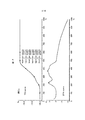
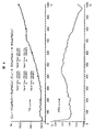
- the thermal analysis result of pure Cu The thermal analysis result of Cu-1wt% Al alloy.
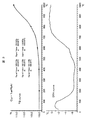
- the thermal analysis result of Cu-3wt% Al alloy The thermal analysis result of Cu-5wt% Al alloy.
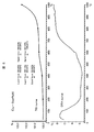
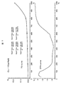
- the thermal analysis result of Cu-10wt% Al alloy The thermal analysis result of Cu-15wt% Al alloy.
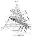
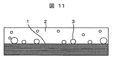
- the thermal analysis result of Cu-10at% Al-5at% Co alloy Relationship between chemical composition, oxidation resistance and electrical resistance in a Cu—Al—Co ternary alloy phase diagram. Explanatory drawing of low electrical resistance expression using a Cu-Al-Co ternary alloy phase diagram. Bubbles generated in dielectric glass on pure Cu wiring.
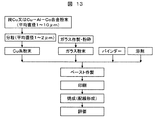
- Test results for the presence or absence of bubbles in dielectric glass on pure Cu and Cu-Al-Co alloy materials Detailed manufacturing process of electronic component wiring manufactured by mixing conductive metal particle powder and glass powder. Transmission electron micrograph of Cu-10 at% Al-10 at% Co alloy wiring. Sectional drawing of the plasma display using the wiring material of this invention. Effect of Cu—Al—Co alloy powder content in conductive metal particle powder and glass powder mixture on specific resistance of electronic component wiring. Sectional drawing of the plasma display using the wiring material of this invention produced by sputtering method. The optical microscope observation result of the bubble which generate
- Sectional drawing of the low-temperature baking glass ceramic multilayer wiring board using the wiring material of this invention The figure explaining the heat processing conditions which bake a multilayer wiring board.
- Sectional drawing which shows the structure of a typical solar cell element.
- the light-receiving surface figure which shows the structure of a typical solar cell element.
- the back view which shows the structure of a typical solar cell element.
- FIG. 1 shows the thermal analysis (TG-DTA) measurement of the pure Cu and Cu—Al based binary alloys used as comparative materials and the Cu—Al—Co based ternary alloy of the present invention in the atmosphere. It is the result of investigating the amount of weight increase due to. 2 to 8, the measurement results are shown in TG curve (thermogravimetry curve: Thermogravimetry curve) and DTA curve (suggested thermal analysis: Differential Thermal analysis curve). Weight gain was plotted against temperature during thermal analysis. In this case, the thermal analysis heating rate was 10 ° C./min. Pure Cu undergoes significant oxidation at a temperature of 200 ° C. or more and increases its weight.
- TG curve thermogravimetry curve: Thermogravimetry curve
- DTA curve suggested thermal analysis: Differential Thermal analysis curve
- the ternary alloy in which Co is added to the Cu-Al alloy exhibits extremely good oxidation resistance even at a high temperature of 800 ° C or higher, where other comparative materials exhibit a remarkable oxidation phenomenon, and the weight increases. There is almost no.
- the Cu—Al—Co ternary alloy used here has a chemical composition of Cu-10 at% Al-5 at% Co (Cu-4.52 wt% Al-4.94 wt% Co in weight%).
- the weight increase at 1000 ° C. was only 0.21%.
- 2 to 7 are the raw data of the actual thermal analysis (TG-DTA) measurement results used in the creation of FIG. 1, and are shown as evidence data in FIG.
- FIG. 9 shows, on the Cu—Al—Co ternary alloy phase diagram, for each fixed point composition, the oxidation weight increase and the electrical resistance when exposed to the air at 1000 ° C. were examined by the thermal analysis method and the 4-terminal method, The results were represented by four classification symbols inserted in the figure and plotted on the state diagram.
- the phase diagram is a Cu—Al—Co ternary alloy phase diagram at 600 ° C.
- the phase state hardly changes near the composition where the symbols are plotted even at higher temperatures.
- atomic% (at%) is clearly shown as a linear grid on the inner side
- weight% (wt% to mass%) is clearly shown on the outer side.
- the arrow A is a hatched area and indicates a Cu solid solution - CoAl compound two-phase area
- the arrow B indicates a composition line in which the Al concentration in the Cu solid solution is lowest in the Cu solid solution - CoAl compound two-phase area. Indicates.
- the inner grid display of the ternary phase diagram in FIG. 9 is atomic% (at%), and the scale display on the outer side of the ternary phase diagram is weight% (wt%).
- FIG. 10 shows the same Cu—Al—Co ternary phase diagram at 600 ° C. as in FIG.
- FIG. 10 shows the same Cu—Al—Co ternary phase diagram at 600 ° C. as in FIG.
- This hatched region is a region where two phases of a Cu solid solution in which Al and Co are dissolved in Cu (expressed as Cu solid solution in the drawing) and a CoAl intermetallic compound (expressed as CoAl compound in the drawing) coexist.
- the higher the Co content in the region the higher the amount of CoAl intermetallic compound formed and the lower the Al concentration in the Cu solid solution.
- the Al concentration in the Cu solid solution is the lowest. That is, since the electrical resistance in the Cu solid solution is lowered as the Al concentration decreases, the amount of Al and Co compound generated increases as the Co content increases in the hatched region, and the Cu solid solution approaches the pure Cu. It can be considered that the electrical resistance value of the Cu solid solution was lowered as a result of changing the composition.
- the Cu content is in the range of 10 at% to 25 at%
- the Co content is in the range of 5 at% to 20 at%
- the electrical resistance value can be 10 ⁇ cm or less, and the increase in oxidation weight when exposed to the air at 1000 ° C. can be 0.5% or less.
- Cu-based material 1 produced by sputtering was embedded in a dielectric glass paste and dried, and then heat-treated in the atmosphere at 610 ° C. for 30 minutes to produce a sputtered wiring structure.
- the Cu—Al—Co ternary alloy of the present invention was used as the Cu-based material 1 and pure Cu was used as a comparative material.
- the oxidation behavior of these Cu-based materials 1 was evaluated by observing the occurrence of bubbles 3 in the dielectric layer 2 with an optical microscope.
- FIG. 12 shows the result of optical microscope observation from the dielectric layer 2 side in FIG.
- an electronic component composed of a conductive metal material in contact with a dielectric glass, a Cu—Al—Co ternary alloy having an Al content of 10 at% to 25 at% and a Co content of 5 at% to 20 at% It was confirmed that it can be applied to metal materials.
- FIG. 13 shows a mixture of Cu—Al—Co alloy particle powder prepared by an atomizing method as conductive metal material powder, glass powder, and pure Cu particle powder prepared using the same method as a comparative material and glass powder.
- the detailed manufacturing process for manufacturing the electronic component wiring will be described.
- the particle powder was divided into particles having a size equal to or smaller than the wiring thickness.
- the particle powder was sized so as to have an average particle diameter of 1 to 2 ⁇ m.
- These conductive metal material particle powder and glass powder were pasted together with a binder and a solvent, formed into a wiring by a printing method, and baked in the atmosphere at 400 ° C.
- the electrical resistance value of the wiring for electronic parts is preferably about 10 ⁇ cm or less.
- the Al content is 10at% to 25at% and the Co content is 5at% to 20at%, so that Cu wiring has sufficient electric conductivity (10 ⁇ cm or less).
- the electric resistance value of the wiring using Ag particles produced by the same method was lower than that of the wiring and can be used as an alternative to Ag wiring.
- the particle powder produced using the atomizing method is a spherical powder, the same effect can be obtained by flaking (plating) with a ball mill or the like, and when the spherical powder and the flake powder are mixed.
- the electrical resistance after firing could be reduced to about 1 ⁇ 2 compared to the case of only spherical shape. Furthermore, when the above atomized powder is heat-treated at a temperature of 500 ° C. or higher in a vacuum, in an inert gas, or in a reducing atmosphere containing hydrogen, the wiring is formed along the process of FIG. Compared with the case where powder was used, the electric resistance value could be reduced to about 40% at the maximum.
- printing is a step of screen printing on a glass substrate
- firing is a step of firing in the atmosphere at 400 ° C. to 800 ° C.
- evaluation is a step of evaluating electrical resistance. It is.
- the wiring shown in FIG. 14 is a wiring produced by the method shown in FIG. 13, and the firing conditions were 800 ° C. for 3 seconds in the air and the heat treatment was performed using a tunnel furnace. In the electron microscope structure, a needle-like CoAl compound is generated in the ground of the Cu solid solution. This supports the above-described mechanism (consideration of FIG. 10) in which the electrical resistance is reduced by the Co addition effect.
- the Al content is 10 at% to 25 at%
- the Co content is 5 at% to 20 at%
- the balance is Cu and inevitable impurities
- the CoAl intermetallic compound Cu-Al-Co ternary alloy conductive metal material with two phases coexisting with glass and glass ceramics, exposed to an oxidizing atmosphere in the manufacturing process, and high-temperature heat treatment at 200 ° C or higher
- the metal material for electronic parts of the present invention is exposed to an oxidizing atmosphere in the production process in a material structure coexisting with glass or glass ceramics, and is a high temperature heat treatment process at 200 ° C. or higher, more substantially 400 ° C. or higher.
- Cu-based wiring, electrodes, and contact parts that do not oxidize can be manufactured by using the electronic parts manufactured by a method including the above. Therefore, it is possible to provide a highly reliable electronic part that is inexpensive and has excellent migration resistance.
- the upper limit confirmation temperature at which the alloy of the present invention is not oxidized is 1050 ° C.
- the wiring, electrodes, and contact parts formed of the metal material for electronic parts made of the Cu—Al—Co ternary alloy of the present invention are a system-on-film (SOF), a tape carrier package (TCP: For electronic parts such as TapeageCarrier , Package, Low Temperature Ceramics (LTCC) Multilayer Wiring Board, Plasma Display (PDP), Liquid Crystal Display (LCD), Organic EL (Electroluminescence) Display, or Solar Cell
- SOF system-on-film
- TCP tape carrier package
- TCP tape carrier package
- PDP Liquid Crystal Display
- LCD Organic EL (Electroluminescence) Display
- Solar Cell The oxidation resistance characteristics of the present invention are effectively exhibited.
- FIG. 1 An outline of a cross-sectional view of the plasma display panel is shown in FIG. 1
- the front plate 10 and the back plate 11 are arranged to face each other with a gap of 100 to 150 ⁇ m, and the gap between the substrates is maintained by the partition walls 12.
- the peripheral portions of the front plate 10 and the back plate 11 are hermetically sealed with a sealing material 13, and the inside of the panel is filled with a rare gas.
- a minute space (cell 14) partitioned by the barrier ribs 12 is filled with a phosphor.
- One pixel is composed of three-color cells filled with red, green, and blue phosphors 15, 16, and 17, respectively. Each pixel emits light of each color according to the signal.
- the front plate 10 and the back plate 11 are provided with regularly arranged electrodes on a glass substrate.
- the display electrode 18 on the front plate 10 and the address electrode 19 on the back plate 11 are paired, and a voltage of 100 to 200 V is selectively applied according to the display signal between them, and ultraviolet rays 20 are generated by the discharge between the electrodes to generate fluorescence.
- the bodies 15, 16, and 17 are caused to emit light and display image information.
- the display electrodes 18 and the address electrodes 19 are covered with dielectric layers 21 and 22 in order to protect these electrodes and to control wall charges during discharge. A thick glass film is used for the dielectric layers 21 and 22.
- a partition wall 12 is provided on the dielectric layer 22 of the address electrode 19 in order to form the cell 14.
- the partition 12 is a stripe-like or box-like structure.
- an Ag thick film wiring is generally used at present.
- Cu is formed during the formation and firing of Cu thick film wiring in an oxidizing atmosphere. Oxidation does not reduce electrical resistance, formation of a dielectric layer in an oxidizing atmosphere, Cu reacts with the dielectric layer during firing, Cu is oxidized and electrical resistance does not decrease, and there is a gap in the vicinity of the Cu thick film wiring ( For example, there is a condition that bubbles are not generated and the pressure resistance is not lowered.
- the display electrodes 18 and the address electrodes 19 can be formed by a sputtering method, but a printing method is advantageous for reducing the price.
- the dielectric layers 21 and 22 are generally formed by a printing method.
- the display electrode 18, the address electrode 19, and the dielectric layers 21 and 22 formed by the printing method are generally baked in an oxidizing atmosphere at a temperature range of 450 to 620 ° C.
- a dielectric layer 21 is formed on the entire surface.
- a protective layer 23 is formed on the dielectric layer 21 to protect the display electrode 18 and the like from discharge. In general, an MgO vapor deposition film is used for the protective layer 23.
- the dielectric layer 22 is formed in the cell formation region, and the partition 12 is provided thereon.
- the partition wall made of a glass structure is made of a structural material containing at least a glass composition and a filler, and is composed of a fired body obtained by sintering the structural material.
- the partition wall 12 is formed by attaching a volatile sheet with a groove cut to the partition wall portion, pouring a partition paste into the groove, and baking it at 500 to 600 ° C., thereby volatilizing the sheet and forming the partition wall 12. Can do.
- partition wall paste may be formed by applying partition wall paste on the entire surface by printing, masking after drying, removing unnecessary portions by sandblasting or chemical etching, and baking at 500 to 600 ° C. it can.
- the cells 14 separated by the barrier ribs 12 are filled with pastes of phosphors 15, 16, and 17 of each color and fired at 450 to 500 ° C. to form the phosphors 15, 16, and 17, respectively.
- the front plate 10 and the back plate 11 that are separately manufactured are opposed to each other, aligned accurately, and the peripheral portion is sealed with glass at 420 to 500 ° C.
- the sealing material 13 is formed in advance on the peripheral edge of either the front plate 10 or the back plate 11 by a dispenser method or a printing method. In general, the sealing material 13 is formed toward the back plate 11. In addition, the sealing material 13 may be temporarily fired in advance simultaneously with the firing of the phosphors 15, 16, and 17. By adopting this method, it is possible to remarkably reduce bubbles in the glass sealing portion, and a highly airtight, that is, highly reliable glass sealing portion is obtained. In the glass sealing, the gas inside the cell 14 is exhausted while heating, and a rare gas is enclosed, whereby the panel is completed.
- the sealing material 13 When the sealing material 13 is pre-fired or sealed with glass, the sealing material 13 may come into direct contact with the display electrode 18 or the address electrode 19, and the wiring material forming the electrode reacts with the sealing material 13. Therefore, it is not preferable to increase the electrical resistance of the wiring material, and it is necessary to prevent this reaction.
- a voltage is applied at a portion where the display electrode 18 and the address electrode 19 intersect to discharge the rare gas in the cell 14 to obtain a plasma state. Then, using the ultraviolet rays 20 generated when the rare gas in the cell 14 returns from the plasma state to the original state, the phosphors 15, 16 and 17 are caused to emit light, the panel is turned on, and image information is displayed. .
- address discharge is performed between the display electrode 18 and the address electrode 19 of the cell 14 to be lit, and wall charges are accumulated in the cell.
- display discharge occurs only in the cells in which wall charges are accumulated by address discharge, and ultraviolet light 20 is generated to cause the phosphor to emit light, thereby displaying image information. Is done.
- the wiring material comprising the Cu—Al—Co alloy powder and glass powder of the present invention can be applied to the display electrode 18 of the front plate 10 and the address electrode 19 of the back plate 11.
- Cu—Al—Co alloy powder having an average particle diameter of 1 to 2 ⁇ m and glass powder having an average particle diameter of 1 ⁇ m were blended in various proportions, and a binder and a solvent were added to prepare a wiring paste.
- As the glass powder lead-free low-temperature softened glass having a softening point of about 450 ° C., ethyl cellulose as a binder, and butyl carbitol acetate as a solvent were used.
- FIG. 16 shows the relationship between the content of the Cu—Al—Co alloy powder of the present invention and the specific resistance of the wiring.
- the specific resistance of the wiring is sufficiently low with almost no oxidation. Was confirmed. Therefore, by setting the glass powder content to 25 vol.% Or less, the Cu—Al—Co alloy powder of the present invention can be used as a wiring material.
- the content of the Cu—Al—Co alloy powder is 85 vol.% Or more (the glass powder content is 15 vol.% Or less), better oxidation resistance can be imparted. It is more preferable that the content of the alloy powder is 85 vol.% Or more.
- the chemical composition of the Cu—Al—Co alloy powder can be imparted with oxidation resistance by adding 10 at% to 25 at% Al to Cu and simultaneously adding 5 at% or more of Co to Cu.
- the Co content is added up to 20 at% along the composition line where the Al concentration in the Cu solid solution indicated by the dotted line is the lowest. Therefore, sufficient oxidation resistance and low electrical resistance characteristics can be secured.
- this Cu—Al—Co alloy powder contained inevitable impurities.
- the wiring is easily peeled off from the glass substrate as the front plate and the back plate.
- the glass powder content was 3 vol. (Volume)% or more, the wiring could be firmly formed on the glass substrate. That is, when the content of the Cu—Al—Co alloy powder is 65 to 97 vol.% And the content of the glass powder is 3 to 35 vol.%, It can be effectively used as a wiring material.
- the upper limit of the glass powder content is preferably 25 vol.% Or less, more preferably 15 vol.% Or less.
- the low thermal expansion filler powder is further mixed with the wiring material, the wiring becomes more difficult to peel.
- the mixing amount is usually required to be 20 vol.% Or less.
- a wiring material comprising 85 vol.% Of Cu—Al—Co alloy powder having an average particle diameter of 1 to 2 ⁇ m and 15 vol.% Of glass powder having an average particle diameter of 1 ⁇ m is selected.
- the plasma display panel shown in FIG. 15 was prototyped by applying it to the display electrode 18 and the address electrode 19 of the back plate 11.
- This wiring material was mixed with ethyl cellulose as a binder and butyl carbitol acetate as a solvent in the same manner as described above to obtain a wiring paste.
- glass of dielectric layers 21 and 22 was coated thereon.
- the glass of the dielectric layers 21 and 22 is made by adding a panda and a solvent to glass powder having an average particle diameter of 1 ⁇ m to form a paste, which is applied to almost the entire surface by a printing method and baked at 610 ° C. for 30 minutes in the atmosphere.
- As the glass powder lead-free glass having a softening point of around 560 ° C., ethyl cellulose as a binder, and butyl carbitol acetate as a solvent were used.
- the front plate 10 and the back plate 11 were produced separately, and the plasma display panel was produced by glass-sealing an outer peripheral part.
- the display electrode 18 and the address electrode 19 using the wiring material of the present invention are not discolored due to oxidation, and there are no voids at the interface between the display electrode 18 and the dielectric layer 21 and between the address electrode 19 and the dielectric layer 22. It was found that it can be mounted on a panel.
- the panel could be lit without the electrical resistance of the display electrode 18 and the address electrode 19 being increased, without the breakdown voltage being lowered, and without migration like Ag. There were no other problems.
- the wiring material of the present invention is not limited to a plasma display panel, and can also be applied as a wiring material for solar cells and the like. At present, a wiring material made of Ag powder and glass powder is also used for the wiring of the solar cell, and the cost can be greatly reduced by changing to the wiring material of the present invention.
- wiring materials were formed on the display electrodes 18 and the address electrodes 19 by sputtering.
- a metal Cr film 24, a Cu—Al—Co alloy film 25 of the present invention, and a metal Cr film 26 are formed again in this order to form a three-layer structure.
- the first metal Cr film 24 improves the adhesion between the front plate 10 and the rear plate 11 and the Cu—Al—Co alloy film, and the third metal Cr film 26 forms a contact with the dielectric layers 21 and 22. Formed to improve wettability.
- Each film thickness is 0.2 ⁇ m for the first-layer metal Cr film 24, 3.0 ⁇ m for the second-layer Cu—Al—Co alloy film 25, and 0.1 ⁇ m for the third-layer metal Cr film 26.
- a plasma display panel was prepared and evaluated in the same manner as in Example 1.
- As the sputtering target a disk made of a metallic Cr bulk material and a Cu—Al alloy bulk material was used for forming each layer.
- the side surfaces of the display electrode 18 and the address electrode 19 using the wiring material of the present invention can be mounted on a panel without generating a gap. Subsequently, as a result of a lighting test of the produced plasma display panel, the electrical resistance of the display electrode 18 and the address electrode 19 is not increased, the breakdown voltage is not lowered, and migration is performed like Ag. There was no panel lighting. There were no other problems.
- the second layer Cu—Al—Co alloy film 25 of the wiring material was changed to a pure Cu film and mounted on the display electrode 18 and the address electrode 19, and a panel was manufactured in the same manner as described above.
- the display electrode 18 and the address electrode 19 made of the above three-layer wiring by the sputtering method gave a favorable panel evaluation result
- the display electrode 18 and the address electrode were then formed with the two-layer wiring by removing the third layer metal Cr film 26.
- the plasma display panel of FIG. 15 was fabricated.
- the film thickness was set to 0.2 ⁇ m for the first-layer metal Cr film 24 and 3.0 ⁇ m for the second-layer Cu—Al—Co alloy film 25 as described above.
- the display electrode 18 and the address electrode 19 using the wiring material of the present invention are not discolored due to oxidation, and there are no voids at the interface between the display electrode 18 and the dielectric layer 21 and between the address electrode 19 and the dielectric layer 22. It was found that it can be mounted on a panel. Subsequently, as a result of conducting a lighting test of the produced plasma display panel, it was found that there was no problem as described above, and that a good panel could be produced even with two-layer wiring.
- the second layer Cu—Al—Co alloy film 25 of the wiring material is changed to a pure Cu film and mounted on the display electrode 18 and the address electrode 19, and the panel is formed in the same manner as described above.
- Prototype The pure Cu films of the display electrode 18 and the address electrode 19 were remarkably oxidized, and many voids were generated at the interface with the dielectric layers 21 and 22.
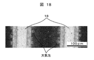
- FIG. 18 shows the result of observation with an optical microscope of large bubbles generated between a wiring formed of a pure Cu film and a dielectric layer. This bubble is generated when the oxide layer generated on the surface of the wiring material reacts with the dielectric at a high temperature. Therefore, pure Cu wiring cannot be applied to the panel.
- the display electrode made of a Cu—Al—Co alloy with Cr As described above, by using a display electrode made of a Cu—Al—Co alloy with Cr as the lowermost layer, it is possible to suppress the generation of bubbles due to reaction with the dielectric regardless of the presence or absence of Cr as the uppermost layer. Similarly, the adhesion between the Cu—Al—Co alloy and the back plate can be maintained even if the lowermost layer is a Cr oxide layer.
- the color tone of the display electrode seen from the front can be adjusted by using a Cr oxide layer with an adjusted thickness at the bottom layer and allowing the reflected light from the Cr oxide surface to interfere with the Cu—Al—Co alloy surface. For example, it can be black to dark or brown.
- Example 2 In the panel trial production of Example 2, the sputtering target of the Cu—Al—Co alloy film applied to the wiring material was examined. In Example 2, a sputter target made of a Cu—Al—Co alloy was used. In this example, it was confirmed whether a desired Cu—Al—Co alloy film could be formed using other sputtering targets.
- a sputter target in which Cu, Al and Co do not form an alloy and each constitutes a target as a single metal was manufactured.
- this sputter target a large number of through holes are formed in a pure Cu disk 27, and pure Al 28 and pure Co 28, which are in the shape of the through holes, are sealed and subjected to surface polishing.
- the size and number of through holes were determined in consideration of the composition uniformity of the sputtered film.
- the through-hole is circular (cylindrical), but it may be strip-shaped (rectangular), or may be a target in which Cu, Al, and Co metal having a fan-shaped target surface shape are alternately combined.
- a Cu—Al—Co alloy film equivalent to a sputter target made of a Cu—Al—Co alloy is obtained. It was. That is, it was found that a sputtered film that hardly changes in resistance due to oxidation and that hardly reacts with the glass of the dielectric layer can also be obtained by the sputter target of this example.
- a Cu—Al—Co alloy having predetermined Al and Co contents can be formed by a plurality of sputter targets using a sputter target of simple Cu and a sputter target of simple Al and simple Co.
- sputtering is performed while rotating a plurality of targets, or Cu, Al, and Co are sputtered repeatedly while changing the target to be sputtered to form a multilayer film of Cu, Al, and Co, and the multilayer film is heat-treated.
- a method of forming a Cu—Al—Co alloy or the like can be used.
- the sputter target of this example can be manufactured at a lower cost than a sputter target made of a Cu—Al—Co alloy.
- a sputter target made of a Cu—Al—Co alloy needs to be manufactured from a bulk base material of a Cu—Al—Co alloy, but the sputter target of this example is pure Cu and pure Al, which are widely used in the world. And there is a merit that can be manufactured by combining pure Co.
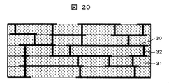
- an LTCC (Low Temperature Co-fired Ceramic) multilayer wiring substrate (5 layers) shown in FIG. 20 was manufactured.
- the wiring 30 is formed three-dimensionally.
- a green sheet 31 made of glass powder and ceramic powder is prepared, and a through hole 32 is opened at a desired position.
- the wiring 30 paste is applied by a printing method, and the through holes 32 are filled. If necessary, the wiring 30 paste is also applied to the back surface of the green sheet 31 by a printing method. At that time, the wiring 30 paste applied on the surface is dried. Green sheets 31 each formed with a paste for wiring 30 are stacked and fired at about 900 ° C. in the atmosphere, and an LTCC multilayer wiring board is manufactured.
- the paste for the wiring 30 an expensive Ag paste is usually used.
- an inexpensive Cu paste which is advantageous for migration countermeasures, it is fired in a nitrogen atmosphere, but debinding is not successful and it is difficult to obtain a dense multilayer wiring board.
- the electrical resistance of the wiring 30 is increased because Cu is oxidized by the softening and flow of the glass at the portion where the glass in the green sheet 31 is in contact with the Cu wiring 30.
- voids due to reaction with glass may occur at the interface. This is an undesirable phenomenon because the wiring 30 may be disconnected.
- the Cu—Al—Co alloy powder of the present invention (average particle size: 1 ⁇ m) was used as the wiring 30 paste. Nitrocellulose with little carbon residue was used as the binder, and butyl acetate was used as the solvent.
- a multilayer wiring board (5 layers) shown in FIG. 15 was manufactured using the paste for wiring 30 composed of these materials.
- the heat treatment condition for firing this multilayer wiring board is that the Cu—Al—Co alloy of the present invention (in this example, Cu-10 at% Al-5 at% Co) is not completely oxidized up to 1050 ° C. in an oxidizing atmosphere.
- the manufactured multilayer wiring board had been completely debaked by 700 ° C., and thus was densely fired. Further, the Cu—Al—Co alloy wiring 30 was hardly oxidized and the electric resistance was not increased. Furthermore, there is no void in the vicinity of the wiring due to the reaction with glass, and it is possible to provide a multilayer wiring board that achieves both high performance and low cost.
- the temperature profile and atmosphere used for the heat treatment are not limited to this.
- the Al content is 10 at% to 25 at%, the Co content is 5 at% to 20 at%, and the balance is Cu and inevitable impurities. The same effect could be obtained by heat treatment.
- FIGS. 1-10 In this example, an example in which the electrode of the present invention is applied to an electrode of a solar cell element will be described.
- Cross-sectional views of typical solar cell elements, and outlines of the light-receiving surface and the back surface are shown in FIGS.
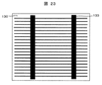
- the semiconductor substrate 130 of the solar cell element contains boron or the like and is a p-type semiconductor. On the light receiving surface side, irregularities are formed by etching in order to suppress reflection of sunlight.
- the light-receiving surface is doped with phosphorus or the like to form an n-type semiconductor diffusion layer 131 with a thickness on the order of submicrons, and a pn junction is formed at the boundary with the p-type bulk portion.
- an antireflection layer 132 such as silicon nitride is formed on the light receiving surface with a film thickness of about 100 nm by vapor deposition or the like.
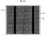
- the formation of the light receiving surface electrode 133 formed on the light receiving surface, and the current collecting electrode 134 and the output extraction electrode 135 formed on the back surface will be described.
- a silver electrode paste containing glass powder is used for the light-receiving surface electrode 133 and the output extraction electrode 145, and an aluminum electrode paste containing glass powder is used for the collecting electrode 134, which are applied by screen printing.
- the electrode is formed by firing at about 500 to 800 ° C. in the atmosphere.
- the glass composition contained in the light receiving surface electrode 133 reacts with the antireflection layer 132 to electrically connect the light receiving surface electrode 133 and the diffusion layer 131.
- aluminum in the current collecting electrode 134 is diffused to the back surface of the semiconductor substrate 130 to form an electrode component diffusion layer 136, whereby the space between the semiconductor substrate 130, the current collecting electrode 134, and the output extraction electrode 135. Ohmic contact can be obtained.
- the solar cell elements shown in FIGS. Prototype By using the same Cu—Al—Co metal particles and phosphoric acid solution as used in Example 1 and applying them to the light receiving surface electrode 133 and the output extraction electrode 135, the solar cell elements shown in FIGS. Prototype. 30 parts by weight of the phosphoric acid solution was added to 100 parts by weight of the Cu—Al—Co metal particles, and the metal particles were dispersed in the phosphoric acid solution by applying ultrasonic waves for 30 minutes. This was used as a paste for the light-receiving surface electrode 133 and the output extraction electrode 135.
- the aluminum electrode paste for the current collecting electrode 134 was applied to the back surface of the semiconductor substrate 130 by screen printing as shown in FIGS. 22 and 24, dried, and then heated to 600 ° C. in the atmosphere in an infrared rapid heating furnace. .
- the holding time at 600 ° C. was 3 minutes.
- the current collecting electrode 134 was first formed on the back surface of the semiconductor substrate 130.
- the light receiving surface electrode 133 and the semiconductor substrate 130 on which the diffusion layer 131 was formed were electrically connected on the light receiving surface. Further, an electrode component diffusion layer 136 was formed on the back surface, and an ohmic contact could be obtained between the semiconductor substrate 130, the current collecting electrode 134, and the output extraction electrode 135. Furthermore, a high-temperature and high-humidity test at 85 ° C. and 85% was conducted for 100 hours, and the wiring resistance and contact resistance of the electrode were hardly increased.
- each electrode can be formed by heat-treating the light-receiving surface and the back surface at 800 ° C. for 3 seconds, and if it is 1050 ° C. or less, it is possible to select heat treatment conditions suitable for various solar cell element structures. I understood.
- the electrode of the present invention can be developed as an electrode of a solar cell element as in the plasma display panel described in Example 1. Moreover, since it can substitute for an expensive Ag electrode, it can also contribute to cost reduction.
- the present invention is not limited to these two electronic components but can be widely applied as electrodes of other electronic components. .
Landscapes
- Chemical & Material Sciences (AREA)
- Engineering & Computer Science (AREA)
- Materials Engineering (AREA)
- Mechanical Engineering (AREA)
- Metallurgy (AREA)
- Organic Chemistry (AREA)
- Dispersion Chemistry (AREA)
- Microelectronics & Electronic Packaging (AREA)
- Parts Printed On Printed Circuit Boards (AREA)
- Powder Metallurgy (AREA)
- Physical Vapour Deposition (AREA)
- Conductive Materials (AREA)
Abstract
Description


β;AlCu3
γ1;Al4Cu9
δ;~Al2Cu3 (<680℃)
ε2;~Al2Cu3(<850-560℃)
η1;AlCu
τ;Al5CoCu4
ω;~Al6CoCu3
κ;~Al3CoCu
ψ;~Al10Co3Cu
2,21,22 誘電体層
3 泡
10 前面板
11 背面板
12 隔壁
13 封着材料
14 セル
15,16,17 赤色,緑色,青色の蛍光体
18 表示電極
19 アドレス電極
20 紫外線
23 保護層
24,26 金属クロム膜
25 Cu-Al-Co合金膜
27 純Cuの円板
28 純Al及び純Co
30 配線
31 グリーンシート
32 貫通孔
130 半導体基板
131 拡散層
132 反射防止層
133 受光面電極
134 集電電極
135 出力取出し電極
136 電極成分拡散層
Claims (10)
- 電極または配線を有する電子部品であって、前記電極または配線の一部または全部が、Al含有量:10at%~25at%,Co含有量:5at%~20at%、残部がCu及び不可避不純物で構成される化学組成を有し、CuにAlとCoが溶け込んだCu固溶体と、CoAl金属間化合物の2相が共存した3元系合金であることを特徴とする電子部品。
- 請求項1において、前記電極または配線が、ガラスまたはガラスセラミックス部材と接する構造を有することを特徴とする電子部品。
- 請求項1において、前記電極・配線はスパッタリング法により基板上に形成され、ガラス或いはガラスセラミックスにより被覆,焼成されたことを特徴とする電子部品。
- 請求項1において、前記電極・配線がさらにガラス成分を含むことを特徴とする電子部品。
- 請求項1において、前記電極または配線が印刷法によってガラス或いはガラスセラミックスのグリーンシートの空孔部及び表面に形成され、該グリーンシートを積層,焼成し、該配線が三次元的に組み込まれたことを特徴とする電子部品。
- 請求項1に記載の電子部品が、システムオンフィルム,テープキャリアパッケージ,低温焼成セラミックス,プラズマディスプレイ,液晶ディスプレイ,有機ELディスプレイ、あるいは太陽電池のいずれかであることを特徴とする電子部品。
- 少なくとも導電性金属材料粉末とガラス粉末を混合した電極・配線用材料であって、該導電性金属材料粉末が、Al含有量:10at%~25at%,Co含有量:5at%~20at%、残部がCu及び不可避不純物で構成される化学組成を有する3元系合金であることを特徴とする電極・配線用材料。
- 請求項7において、前記導電性金属材料粉末が、球状及び板状の粒子粉末の成形形態を有することを特徴とする電極・配線用材料。
- 請求項7において、前記導電性金属材料電子粉末が75~97vol.%、及び前記ガラス粉末が3~25vol.%からなることを特徴とする電極・配線用材料。
- 請求項7に記載の電極・配線用材料に樹脂バインダー又は溶剤を混合して構成されることを特徴とする電極・配線用ペースト材料。
Priority Applications (2)
| Application Number | Priority Date | Filing Date | Title |
|---|---|---|---|
| US13/263,359 US8790549B2 (en) | 2009-04-10 | 2010-04-08 | Electronic component provided with Cu—Al—Co-based alloy electrode or wiring |
| JP2011508252A JP5474936B2 (ja) | 2009-04-10 | 2010-04-08 | Cu−Al−Co系合金の電極・配線を具備した電子部品及びCu−Al−Co系合金の電極・配線用材料ならびにそれを用いた電極・配線用ペースト材料 |
Applications Claiming Priority (2)
| Application Number | Priority Date | Filing Date | Title |
|---|---|---|---|
| JP2009095628 | 2009-04-10 | ||
| JP2009-095628 | 2009-04-10 |
Publications (1)
| Publication Number | Publication Date |
|---|---|
| WO2010116746A1 true WO2010116746A1 (ja) | 2010-10-14 |
Family
ID=42936040
Family Applications (1)
| Application Number | Title | Priority Date | Filing Date |
|---|---|---|---|
| PCT/JP2010/002573 Ceased WO2010116746A1 (ja) | 2009-04-10 | 2010-04-08 | Cu-Al-Co系合金の電極・配線を具備した電子部品 |
Country Status (3)
| Country | Link |
|---|---|
| US (1) | US8790549B2 (ja) |
| JP (1) | JP5474936B2 (ja) |
| WO (1) | WO2010116746A1 (ja) |
Cited By (2)
| Publication number | Priority date | Publication date | Assignee | Title |
|---|---|---|---|---|
| JPWO2019111491A1 (ja) * | 2017-12-04 | 2020-12-10 | 株式会社カネカ | 太陽電池およびその太陽電池を備えた電子機器 |
| JPWO2022172785A1 (ja) * | 2021-02-09 | 2022-08-18 |
Citations (6)
| Publication number | Priority date | Publication date | Assignee | Title |
|---|---|---|---|---|
| JPH08125341A (ja) * | 1994-10-25 | 1996-05-17 | Hitachi Ltd | 電子回路装置 |
| JPH09199976A (ja) * | 1996-01-18 | 1997-07-31 | Hitachi Ltd | 弾性表面波素子電極 |
| JP2002294437A (ja) * | 2001-04-02 | 2002-10-09 | Mitsubishi Materials Corp | 銅合金スパッタリングターゲット |
| JP2003277170A (ja) * | 2002-03-26 | 2003-10-02 | Kyocera Corp | 配線導体用組成物 |
| JP2004207009A (ja) * | 2002-12-25 | 2004-07-22 | Kyocera Corp | 銅メタライズ組成物、並びに、配線基板およびその製法 |
| JP2007305528A (ja) * | 2006-05-15 | 2007-11-22 | Fujitsu Hitachi Plasma Display Ltd | プラズマディスプレイパネルおよびその製造方法 |
Family Cites Families (4)
| Publication number | Priority date | Publication date | Assignee | Title |
|---|---|---|---|---|
| US2130737A (en) * | 1937-09-15 | 1938-09-20 | Mallory & Co Inc P R | Copper alloy |
| US5468310A (en) * | 1993-02-01 | 1995-11-21 | Nissan Motor Co., Ltd. | High temperature abrasion resistant copper alloy |
| JP3754011B2 (ja) | 2002-09-04 | 2006-03-08 | デプト株式会社 | 電子部品用金属材料、電子部品、電子機器、金属材料の加工方法、電子部品の製造方法及び電子光学部品 |
| GB0512836D0 (en) * | 2005-06-21 | 2005-08-03 | Jha Animesh | Inert alloy anodes for aluminium electrolysis cell using molten salt bath confidential |
-
2010
- 2010-04-08 US US13/263,359 patent/US8790549B2/en not_active Expired - Fee Related
- 2010-04-08 WO PCT/JP2010/002573 patent/WO2010116746A1/ja not_active Ceased
- 2010-04-08 JP JP2011508252A patent/JP5474936B2/ja not_active Expired - Fee Related
Patent Citations (6)
| Publication number | Priority date | Publication date | Assignee | Title |
|---|---|---|---|---|
| JPH08125341A (ja) * | 1994-10-25 | 1996-05-17 | Hitachi Ltd | 電子回路装置 |
| JPH09199976A (ja) * | 1996-01-18 | 1997-07-31 | Hitachi Ltd | 弾性表面波素子電極 |
| JP2002294437A (ja) * | 2001-04-02 | 2002-10-09 | Mitsubishi Materials Corp | 銅合金スパッタリングターゲット |
| JP2003277170A (ja) * | 2002-03-26 | 2003-10-02 | Kyocera Corp | 配線導体用組成物 |
| JP2004207009A (ja) * | 2002-12-25 | 2004-07-22 | Kyocera Corp | 銅メタライズ組成物、並びに、配線基板およびその製法 |
| JP2007305528A (ja) * | 2006-05-15 | 2007-11-22 | Fujitsu Hitachi Plasma Display Ltd | プラズマディスプレイパネルおよびその製造方法 |
Cited By (3)
| Publication number | Priority date | Publication date | Assignee | Title |
|---|---|---|---|---|
| JPWO2019111491A1 (ja) * | 2017-12-04 | 2020-12-10 | 株式会社カネカ | 太陽電池およびその太陽電池を備えた電子機器 |
| JP7146805B2 (ja) | 2017-12-04 | 2022-10-04 | 株式会社カネカ | 太陽電池およびその太陽電池を備えた電子機器 |
| JPWO2022172785A1 (ja) * | 2021-02-09 | 2022-08-18 |
Also Published As
| Publication number | Publication date |
|---|---|
| US20120285733A1 (en) | 2012-11-15 |
| JP5474936B2 (ja) | 2014-04-16 |
| JPWO2010116746A1 (ja) | 2012-10-18 |
| US8790549B2 (en) | 2014-07-29 |
Similar Documents
| Publication | Publication Date | Title |
|---|---|---|
| JP4709238B2 (ja) | Cu系配線用材料およびそれを用いた電子部品 | |
| CN102318013B (zh) | 导电性浆料及具备使用其的电极配线的电子部件 | |
| JP2010161331A (ja) | 電極,電極ペースト及びそれを用いた電子部品 | |
| CN103052605B (zh) | 电极用玻璃组合物、使用该组合物的电极膏、以及使用该电极膏的电子部件 | |
| JP5497504B2 (ja) | 電子部品 | |
| JP5699933B2 (ja) | ガラス組成物およびそれを用いた導電性ペースト組成物、電極配線部材と電子部品 | |
| WO2011016217A1 (ja) | Cu-Al合金粉末、それを用いた合金ペーストおよび電子部品 | |
| TWI478890B (zh) | An electronic component, a conductive paste for an aluminum electrode thereof, and a glass composition for an aluminum electrode | |
| TWI471283B (zh) | An electronic component, a conductive paste for an aluminum electrode thereof, and a glass composition for an aluminum electrode | |
| JP5474936B2 (ja) | Cu−Al−Co系合金の電極・配線を具備した電子部品及びCu−Al−Co系合金の電極・配線用材料ならびにそれを用いた電極・配線用ペースト材料 | |
| JP5747096B2 (ja) | 導電性ペースト | |
| JP5517495B2 (ja) | 配線部材、その製造方法及びそれを用いた電子部品 | |
| JP5480360B2 (ja) | 電子部品、導電性ペーストおよび電子部品の製造方法 | |
| JP2011066353A (ja) | 太陽電池用アルミニウムペースト |
Legal Events
| Date | Code | Title | Description |
|---|---|---|---|
| 121 | Ep: the epo has been informed by wipo that ep was designated in this application |
Ref document number: 10761450 Country of ref document: EP Kind code of ref document: A1 |
|
| ENP | Entry into the national phase |
Ref document number: 2011508252 Country of ref document: JP Kind code of ref document: A |
|
| NENP | Non-entry into the national phase |
Ref country code: DE |
|
| WWE | Wipo information: entry into national phase |
Ref document number: 13263359 Country of ref document: US |
|
| 122 | Ep: pct application non-entry in european phase |
Ref document number: 10761450 Country of ref document: EP Kind code of ref document: A1 |