WO2010113722A1 - Dispositif de capture d'image à semi-conducteurs - Google Patents
Dispositif de capture d'image à semi-conducteurs Download PDFInfo
- Publication number
- WO2010113722A1 WO2010113722A1 PCT/JP2010/055086 JP2010055086W WO2010113722A1 WO 2010113722 A1 WO2010113722 A1 WO 2010113722A1 JP 2010055086 W JP2010055086 W JP 2010055086W WO 2010113722 A1 WO2010113722 A1 WO 2010113722A1
- Authority
- WO
- WIPO (PCT)
- Prior art keywords
- pixel
- holding
- amplifying
- solid
- transistor
- Prior art date
Links
- 238000006243 chemical reaction Methods 0.000 claims abstract description 10
- 238000003384 imaging method Methods 0.000 claims description 49
- 238000012546 transfer Methods 0.000 claims description 35
- 230000003321 amplification Effects 0.000 claims description 29
- 238000003199 nucleic acid amplification method Methods 0.000 claims description 29
- 238000000034 method Methods 0.000 claims description 7
- 238000010586 diagram Methods 0.000 description 14
- 239000003990 capacitor Substances 0.000 description 9
- 238000009825 accumulation Methods 0.000 description 8
- 238000012986 modification Methods 0.000 description 3
- 230000004048 modification Effects 0.000 description 3
- 230000035945 sensitivity Effects 0.000 description 3
- 230000015556 catabolic process Effects 0.000 description 2
- 230000008602 contraction Effects 0.000 description 2
- 238000006731 degradation reaction Methods 0.000 description 2
- 238000013459 approach Methods 0.000 description 1
- 238000010438 heat treatment Methods 0.000 description 1
- 238000012545 processing Methods 0.000 description 1
Images


Classifications
-
- H—ELECTRICITY
- H04—ELECTRIC COMMUNICATION TECHNIQUE
- H04N—PICTORIAL COMMUNICATION, e.g. TELEVISION
- H04N25/00—Circuitry of solid-state image sensors [SSIS]; Control thereof
- H04N25/70—SSIS architectures; Circuits associated therewith
- H04N25/76—Addressed sensors, e.g. MOS or CMOS sensors
- H04N25/78—Readout circuits for addressed sensors, e.g. output amplifiers or A/D converters
-
- H—ELECTRICITY
- H04—ELECTRIC COMMUNICATION TECHNIQUE
- H04N—PICTORIAL COMMUNICATION, e.g. TELEVISION
- H04N25/00—Circuitry of solid-state image sensors [SSIS]; Control thereof
- H04N25/70—SSIS architectures; Circuits associated therewith
- H04N25/701—Line sensors
-
- H—ELECTRICITY
- H04—ELECTRIC COMMUNICATION TECHNIQUE
- H04N—PICTORIAL COMMUNICATION, e.g. TELEVISION
- H04N25/00—Circuitry of solid-state image sensors [SSIS]; Control thereof
- H04N25/70—SSIS architectures; Circuits associated therewith
- H04N25/71—Charge-coupled device [CCD] sensors; Charge-transfer registers specially adapted for CCD sensors
- H04N25/75—Circuitry for providing, modifying or processing image signals from the pixel array
-
- H—ELECTRICITY
- H04—ELECTRIC COMMUNICATION TECHNIQUE
- H04N—PICTORIAL COMMUNICATION, e.g. TELEVISION
- H04N25/00—Circuitry of solid-state image sensors [SSIS]; Control thereof
- H04N25/70—SSIS architectures; Circuits associated therewith
- H04N25/76—Addressed sensors, e.g. MOS or CMOS sensors
- H04N25/77—Pixel circuitry, e.g. memories, A/D converters, pixel amplifiers, shared circuits or shared components
- H04N25/771—Pixel circuitry, e.g. memories, A/D converters, pixel amplifiers, shared circuits or shared components comprising storage means other than floating diffusion
-
- H—ELECTRICITY
- H04—ELECTRIC COMMUNICATION TECHNIQUE
- H04N—PICTORIAL COMMUNICATION, e.g. TELEVISION
- H04N2101/00—Still video cameras
Definitions
- the present invention relates to a one-dimensional solid-state imaging device.
- Patent Document 1 describes a solid-state imaging device in which a plurality of pixel portions that perform photoelectric conversion are two-dimensionally arranged.
- solid-state imaging devices include solid-state imaging devices in which a plurality of pixel units that perform photoelectric conversion are one-dimensionally arranged as solid-state imaging devices used for barcode reading and the like.
- the one-dimensional solid-state imaging device can be realized by using one horizontal row or one vertical column of the two-dimensionally arranged pixel units in the two-dimensional solid-state imaging device described in Patent Document 1.
- M holding units are provided for M pixel units.
- transfer from the pixel unit requiring a relatively long time to the holding unit can be simultaneously performed on all the pixel units, and thus high-speed reading is possible.
- M holding units are provided, the circuit scale becomes large. In addition, power consumption during transfer increases.
- one holding unit is provided for M pixel units.
- this solid-state imaging device since there is only one holding portion, it is possible to reduce the size, the price, and the power consumption.
- the transfer from the pixel unit requiring a relatively long time to the holding unit is sequentially performed on all the pixel units, the reading speed is slow.
- an object of the present invention is to provide a solid-state imaging device capable of achieving both miniaturization and high speed.
- the solid-state imaging device has N holdings that sequentially hold output signals from different pixel units among the M pixel units in the solid-state imaging device in which M pixel units that perform photoelectric conversion are arranged. (N is smaller than M) and an amplification unit that sequentially amplifies output signals from the N holding units.
- this solid-state imaging device since the number of holding units is smaller than the number of pixel units, the circuit scale can be reduced, and downsizing, cost reduction, and power consumption can be achieved.
- N holding units since N holding units are provided, transfer from the pixel unit that requires a relatively long time to the holding unit can be performed in parallel with respect to the N pixel units, and the reading speed is increased. Can be speeded up.
- the nth holding unit (n is an integer from 1 to N) among the N holding units described above is an M / N adjacent to the nth pixel unit among the M pixel units at an N interval.
- a plurality of pixel units that sequentially hold transfer signals transferred from the M / N pixel units, and the amplifying unit described above sequentially amplifies read signals read from the N holding units. It is preferable to repeat the treatment periodically.
- the number N of holding units is more appropriately determined so that the reading time required for one cycle of the reading process by the amplification unit approaches the transfer time from the pixel unit to the holding unit. High speed is possible.
- Each of the M pixel portions described above includes a photodiode that performs photoelectric conversion, an amplifying transistor that amplifies an output signal from the photodiode, and an intra-pixel transfer connected between the photodiode and the amplifying transistor.
- a transistor is provided with a pixel reset transistor connected between the amplifying transistor input and the reference voltage terminal, and a transfer transistor connected to the output side of the amplifying transistor. Is preferred.
- the charge generated in the photodiode can be temporarily held in the gate capacitance of the amplifying transistor, so that the next accumulation can be started in the photodiode.
- the start and end of the accumulation can be performed almost simultaneously on all the pixel portions, and the synchronization at the time of image acquisition can be ensured (global shutter).
- Each of the M pixel portions described above includes a photodiode that performs photoelectric conversion, a first amplification transistor that amplifies an output signal from the photodiode, and a second amplification that amplifies the output signal from the first amplification transistor.
- the first amplifying transistor is preferably smaller in size than the second amplifying transistor.
- This configuration can reduce the signal transfer time from the pixel unit to the holding unit without reducing the sensitivity of the photodiode (two-stage amplifier).
- the above-described solid-state imaging device further includes an input / output electrode disposed substantially at the center in the arrangement direction of the M pixel units.
- the input / output electrodes may be peeled off due to thermal contraction or the like.
- the input / output electrodes are arranged substantially at the center, it is possible to reduce peeling due to heat shrinkage or the like.
- FIG. 1 is a diagram illustrating a configuration of a solid-state imaging device according to an embodiment of the present invention.
- FIG. 2 is a circuit diagram of the solid-state imaging device according to the embodiment of the present invention.
- FIG. 3 is a circuit diagram of the pixel portion shown in FIG.
- FIG. 4 is a circuit diagram of the holding circuit shown in FIG.
- FIG. 5 is a circuit diagram of the amplifying unit shown in FIG.
- FIG. 6 is a timing chart showing signal waveforms in the solid-state imaging device of the present embodiment.
- FIG. 7 is a diagram illustrating the operation of the solid-state imaging device of the present embodiment.
- FIG. 8 is a circuit diagram of a pixel portion according to a modification of the present invention.
- FIG. 9 is a circuit diagram of a holding circuit according to a modification of the present invention.
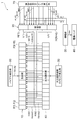
- FIG. 1 is a diagram showing a configuration of a solid-state imaging device according to an embodiment of the present invention
- FIG. 2 is a circuit diagram of the solid-state imaging device according to the embodiment of the present invention.
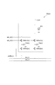
- the solid-state imaging device 1 illustrated in FIGS. 1 and 2 includes a light receiving unit 10, a holding unit 20, an amplification unit 30, an output selection unit 40, an output selection unit timing generation unit 50, a bias generation unit 60, A holding unit timing generator 70 and an electrode pad (input / output electrode) 80 are provided.
- the pixel portions P (1) to P (M) have a common configuration, and include a photodiode that generates an amount of charge corresponding to the amount of incident light, and an in-pixel charge holding portion that holds the charge. is doing.
- the light-receiving unit 10 receives a control signal output from the output selection unit 40 (trans signal, reset signal, hold (m) signal, and address (m) signal, which will be described later) from the photodiode to the in-pixel charge holding unit.
- the output selection unit 40 receives a control signal from the output selection unit timing generation unit 50 and controls the timing of charge transfer within the pixel and transfer of charge to the holding unit 20.
- the pixel units P (1) to P (M) in the light receiving unit 10 operate by receiving bias voltages (reference voltages Vb1 and Vb2 described later) generated by the bias generation unit 60.
- the holding units described in the claims are the holding circuits H (1) to H (N).
- the first holding circuit H (1) includes four pixel portions P (1) adjacent to the first pixel portion P (1) at intervals of four.
- the second holding circuit H (2) is adjacent to the second pixel portion P (2) at four intervals.
- the third holding circuit H (3) includes four pixel portions P (3), P (7), P (11), P, which are adjacent to the third pixel portion P (3) at intervals of four.
- the fourth holding circuit H (4) is connected to four pixel portions P (4) and P (8) adjacent to the fourth pixel portion P (4) at intervals of four. , P (12), P (16).
- the holding circuits H (1) to H (N) sequentially receive voltages transferred from the connected M / N pixel units, and hold these voltage values.
- the holding circuits H (1) to H (N) can hold a voltage value representing a signal component on which a noise component is superimposed, and can also hold a voltage value representing a noise component.
- the holding circuits H (1) to H (N) correspond to control signals (set_s (n) signal, set_n (n) signal, and shift (n) signal described later) from the holding unit timing generation unit 70. The holding timing is controlled.
- the amplifying unit 30 sequentially receives voltages read from the holding unit 20, that is, the holding circuits H (1) to H (N), and periodically repeats a read process for amplifying these voltage values. For example, after sequentially amplifying / outputting the voltage values of the pixel portions P (1), P (2), P (3), and P (4) read sequentially from the holding circuits H (1) to H (4) The voltage values of the pixel portions P (5), P (6), P (7), and P (8) sequentially read from the holding circuits H (1) to H (4) again are sequentially amplified / output, Thereafter, the voltage values of the pixel portions P (9), P (10), P (11), and P (12) sequentially read out from the holding circuits H (1) to H (4) are sequentially amplified / outputted again.
- the amplifying unit 30 outputs the amplified voltage to the outside through the electrode pad 80.
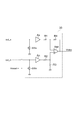
- FIG. 3 is a circuit diagram of the pixel portions P (1) to P (16).
- the pixel portion P (m) employs an APS (Active Pixel Sensor) method, and includes a photodiode PD (m), MOS transistors Tt (m), Tr (m), Th (m), Ta (m), Tamp (m).
- the reference voltage Vb1 is input to the cathode of the photodiode PD (m) via the transistor Tt (m) and the transistor Tr (m) connected in series, and the anode is grounded. A node between the transistor Tt (m) and the transistor Tr (m) is connected to the gate of the amplifying transistor Tamp (m) via the intra-pixel transfer transistor Th (m).
- the reference voltage Vb2 is input to the drain of the amplifying transistor Tamp (m), and the source is connected to the wiring L (n) via the transfer transistor Ta (m).
- the Trans signal is input to the gate of the transistor Tt (m), and the Reset signal is input to the gate of the transistor Tr (m).
- a Hold (m) signal is input to the gate of the transistor Th (m), and an Address (m) signal is input to the gate of the transistor Ta (m).
- These Trans signal, Reset signal, Hold (m) signal, and Address (m) signal are supplied from the output selection unit 40.
- the reference voltages Vb1 and Vb2 are supplied from the bias generator 60.
- the photodiodes PD (1) to PD (16) are reset to the reference potential (Vb1).
- the Trans signal becomes low level, charges are generated in the photodiodes PD (1) to PD (16) in accordance with the external light quantity, and accumulation is started.
- the Trans signal and the Hold (1) to (16) signals become high level, the photodiodes PD (1) to PD (16) to the gate capacitances (in-pixel charge holding portions) of the amplification transistors Tamp (1) to (16). ) Is transferred to the pixel.
- the operation in the global shutter mode in which the start and end of accumulation in all the pixel portions is performed substantially simultaneously is realized.
- the voltage value corresponding to the amount of charge held in the gate capacitance of the amplifying transistor Tamp (m) is sequentially output as a signal component to the wiring L (n) by closing the transistor Ta (m).
- the gate capacitance of the amplifying transistor Tamp (m) is reset by setting the Reset signal and the Hold (m) signal to a high level.
- FIG. 4 is a circuit diagram of the holding circuits H (1) to H (4).
- the holding circuit H (n) includes a capacitive element Cs (n) for holding a signal component output from the pixel portion P (m), and switches SWs1 (n) and SWs2 (n).
- the holding circuit H (n) includes a capacitive element Cn (n) for holding a noise component output from the pixel portion P (m), and switches SWn1 (n) and SWn2 (n). Yes.
- the holding circuit H (n) has a constant current source I (n).
- the switch SWs1 (n) and the switch SWs2 (n) are connected in series between the wiring L (n) and the wiring out_s.
- One end of the capacitive element Cs (n) is connected to a node between the switch SWs1 (n) and the switch SWs2 (n), and the other end of the capacitive element Cs (n) is grounded.
- the switch SWn1 (n) and the switch SWn2 (n) are connected between the wiring L (n) and the wiring out_n.
- One end of the capacitive element Cn (n) is connected to a node between the switch SWn1 (n) and the switch SWn2 (n), and the other end of the capacitive element Cn (n) is grounded.
- the switch SWs1 (n) opens and closes according to the set_s (n) signal, and the switch SWn1 (n) opens and closes according to the set_n (n) signal. Further, the switches SWs2 (n) and SWn2 (n) are opened / closed in response to the shift (n) signal.
- the set_s signal, the set_n signal, and the shift (n) signal are supplied from the holding unit timing generation unit 70.
- the constant current source I (n) is connected to the wiring L (n). As described above, the constant current source I (n) is provided not at the output stage of the pixel unit P (m) but at the input stage of the holding circuit H (n), whereby the pixel unit P (m) and the holding circuit H are provided. A current signal is exchanged with (n). Since the current signal has less signal degradation due to the capacitance of the wiring or the like than the voltage signal, this configuration can reduce the signal degradation due to the capacitance of the wiring L (n) or the like.
- the switch SWs1 (n) is closed / opened according to the set_s signal, whereby the signal component output from the pixel portion P (m) is accumulated / held in the capacitor Cs (n). Is done.
- the switch SWs2 (n) is closed in response to the shift (n) signal, the voltage value held by the capacitor Cs (n) is output to the wiring out_s.
- the switch SWn1 (n) is closed / opened according to the set_n signal, the noise component output from the pixel portion P (m) is accumulated / held in the capacitive element Cn (n).
- the switch SWn2 (n) is closed in accordance with the shiht (n) signal, the voltage value held by the capacitor Cn (n) is output to the wiring out_n.
- FIG. 5 is a circuit diagram of the amplifying unit 30.
- the amplifying unit 30 shown in FIG. 5 includes amplifiers As and An, a differential amplifier Asn, switches SWs and SWn, and resistance elements R1 to R4.
- the input terminal of the amplifier As is connected to the wiring out_s, and the output terminal is connected to the inverting input terminal of the differential amplifier Asn via the resistance element R1.
- the input terminal of the amplifier An is connected to the wiring out_n, and the output terminal is connected to the non-inverting input terminal of the differential amplifier Asn via the resistance element R2.
- the non-inverting input terminal of the differential amplifier Asn is grounded via the resistance element R3, and the output signal of the amplifier An is divided by the series circuit of the resistance elements R2 and R3 at the non-inverting input terminal of the differential amplifier Asn. Voltage is input.
- a feedback resistive element R4 is connected between the output terminal and the inverting input terminal of the differential amplifier Asn, and the output terminal of the differential amplifier Asn is connected to the video output wiring Video.
- switches SWs and SWn are connected between the input terminals of the amplifiers As and An and the ground potential, respectively.
- the switches SWs and SWn open and close according to the Hreset signal. When the switches SWs and SWn are closed, the input terminals of the amplifiers As and An are reset, respectively.
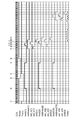
- FIG. 6 is a timing chart showing signal waveforms in the solid-state imaging device
- FIG. 7 is a diagram showing the operation of the solid-state imaging device. (Reset and charge accumulation of pixel portions P (1) to P (16))
- the photodiodes PD (1) to PD (16) in the pixel portions P (1) to P (16) before the time t1 that is, in a period in which the Reset signal and the Trans signal are at a high level. Reset is performed.
- the Trans signal becomes low level at time t1, resetting of the photodiodes PD (1) to PD (16) is completed.
- charge accumulation in the 16 photodiodes PD (1) to PD (16) is performed in the period t1 to t5.
- the gate capacitances of the amplification transistors Tamp (1) to Tamp (16) are set in the periods t2 to t3 by setting the Reset signal and the Hold (1) to Hold (16) signals to a high level. Is reset.
- the photodiodes PD (1) to PD (16) become high level, the photodiodes PD (1) to PD (16) Then, the intra-pixel transfer of charges is performed to the gate capacitors (intra-pixel charge holding units) of the amplification transistors Tamp (1) to Tamp (16) of each pixel.
- the gate capacitance of the amplifying transistor Tamp (1) is reset.
- the Noise component from the pixel portion P (1) is applied to the capacitor Cn (1) in the holding circuit H (1). Transferred.
- the pixel units P (1) to P (16) sequentially transfer charges by gradually delaying the transfer disclosure time.
- the holding circuit H (1) includes four pixel portions P (1), P (5), P (9), and P (13) adjacent to the pixel portion P (1) at intervals of four.
- the voltages transferred from the pixel portions P (1), P (5), P (9), and P (13) are sequentially held and read out sequentially.
- the holding circuit H (2) includes four pixel portions P (2), P (6), P (10), and P (14) that are adjacent to the pixel portion P (2) at intervals of four.
- the voltages transferred from the pixel portions P (2), P (6), P (10), and P (14) are sequentially held and read out sequentially.
- the holding circuit H (3) includes four pixel portions P (3), P (7), P (11), and P (15) that are adjacent to the pixel portion P (3) at intervals of four.
- the holding circuit H (4) includes four pixel portions P (4), P (8), P (12), and P (16) adjacent to the pixel portion P (4) at intervals of four.
- the voltages transferred from the pixel portions P (4), P (8), P (12), and P (16) are sequentially held and read out sequentially.
- the amplifying unit 30 sequentially amplifies the voltage values of the pixel units P (1), P (2), P (3), and P (4) sequentially read out from the holding circuits H (1) to H (4). After the output, the voltage values of the pixel portions P (5), P (6), P (7), and P (8) sequentially read out from the holding circuits H (1) to H (4) again are sequentially amplified / After that, the voltage values of the pixel portions P (9), P (10), P (11), and P (12) that are sequentially read out from the holding circuits H (1) to H (4) are sequentially amplified again.
- the amplifying unit 30 sequentially receives the voltages read from the holding circuits H (1) to H (4), and periodically repeats the reading process for amplifying these voltage values.
- the number of holding circuits H (1) to H (4) is smaller than the number of pixel portions P (1) to P (16), so that the circuit scale can be reduced. Therefore, it is possible to reduce the size, the price, and the power consumption during transfer. Further, according to the solid-state imaging device 1 of the present embodiment, since four holding circuits are provided, the pixel circuits P (1) to P (16) that require a relatively long time to the holding circuits H (1) to H (4). Can be transferred to the four pixel portions in parallel, and the reading speed can be increased.
- the readout time ta required for one cycle of the readout processing by the amplifying unit 30 is the transfer time tb from each of the pixel units P (1) to P (M) to each of the holding circuits H (1) to H (N) ( Since the number N of holding circuits is determined so as to be 1 / (N-1)), even if the transfer time is relatively long, it is possible to increase the speed more appropriately.
- each of the holding circuits H (1) to H (4) can be disposed relatively close to the pixel portions P (1) to P (16).
- the wiring from the parts P (1) to P (16) to the holding circuits H (1) to H (4) can be shortened, and the wiring capacity can be reduced. As a result, the transfer time can be shortened and the reading speed can be increased.
- the IC chip is provided with M holding circuits for M pixel units. Due to the shape, the holding capacitor element has an elongated shape, and the variation in capacitance value increases.
- the holding capacitive elements Cs (1) to Cs (4) and Cn (1) to Cn (4) in the holding circuits H (1) to H (4), respectively. Can be made relatively square, so that variation in capacitance value can be relatively reduced, and as a result, variation in holding circuits H (1) to H (4) can be reduced.
- the light-receiving unit 10 that is, the 16 pixel units P (1) to P (16) are arranged in a line in the longitudinal direction of the IC chip C1, and the output selection unit 40 is also configured with the pixel units P (1) to P (1). Adjacent to P (16), the IC chips C1 are arranged in a line in the longitudinal direction. Below the pixel portions P (1) to P (16) and the output selection portion 40, a holding portion 20, an amplification portion 30, an output selection portion timing generation portion 50, a bias generation portion 60, and a holding portion are provided. A part timing generator 70 and electrode pads (input / output electrodes) 80 are arranged.
- the electrode pad 80 is disposed near the center in the longitudinal direction of the IC chip C1.
- the amplifying unit 30 is disposed in the immediate vicinity of one side of the electrode pad 80, and the holding unit 20 is disposed in the immediate vicinity of the amplifying unit 30.
- a holding unit timing generation unit 70 is disposed in the immediate vicinity of the holding unit 20.
- a bias generator 60 and an output selector timing generator 50 are arranged on the other side of the electrode pad 80.
- the IC chip C1 has a horizontally long shape in the longitudinal direction.
- the IC chip C1 may greatly expand and contract in the longitudinal direction due to heat treatment by an assembly process or the like, and as a result, the electrode pad may be peeled off.
- the electrode pad 80 is disposed near the center in the longitudinal direction of the IC chip C1, peeling due to thermal contraction can be reduced.
- the present invention is not limited to the above-described embodiment, and various modifications can be made.
- the pixel unit P (m) employs a single-stage amplifier configuration including one amplification transistor Tamp (m).
- the pixel unit includes a plurality of amplification transistors. It may be a form provided.
- FIG. 8 shows a pixel portion adopting a two-stage amplifier configuration including two amplifying transistors.
- the pixel unit P (m) having the two-stage amplifier configuration further includes transistors Tamp2 (m), Ta2 (m), Ta3 (m), and the pixel unit P (m) having the one-stage amplifier configuration.
- the constant current source I1 (m) is provided.
- the emitter of the transistor Ta (m) is connected to the gate of the second amplification transistor Tamp2 (m) via the transistor Ta2 (m), and the gate of the second amplification transistor Tamp2 (m) is connected to the transistor Ta3.
- the reference voltage Vb3 is input via (m).
- the collector of the second amplifying transistor Tamp2 (m) is grounded, and the emitter is connected to the wiring L (n).
- a constant current source I1 (m) is connected to the emitter of the transistor Ta (m).
- An Address (m) signal is input to the gates of the transistors Ta2 (m) and Ta3 (m).
- the holding circuit H (n) connected to the pixel unit P (m) having the two-stage amplifier configuration is connected to the constant current source I (n) in the holding circuit H (n) shown in FIG. Instead, it is necessary to provide a constant current source I2 (n) connected to the reference voltage Vb4.
- the size of the amplification transistor Tamp (m) if the size of the amplification transistor Tamp (m) is increased, the charge-voltage conversion of the photodiode PD (m) is caused by the gate capacitance of the amplification transistor Tamp (m). The coefficient becomes worse and the sensitivity becomes worse. Therefore, the size of the amplifying transistor Tamp (m) cannot be increased, and the current flowing through the wiring L (n) is limited.
- the size of the first amplifying transistor Tamp (m) is reduced, and the size of the second amplifying transistor Tamp2 (m) is reduced to that of the first amplifying transistor Tamp (m). It is larger than the size.
Landscapes
- Engineering & Computer Science (AREA)
- Multimedia (AREA)
- Signal Processing (AREA)
- Transforming Light Signals Into Electric Signals (AREA)
- Solid State Image Pick-Up Elements (AREA)
- Facsimile Heads (AREA)
Abstract
Priority Applications (3)
| Application Number | Priority Date | Filing Date | Title |
|---|---|---|---|
| US13/256,726 US20120002091A1 (en) | 2009-03-30 | 2010-03-24 | Solid-state image pickup device |
| EP10758496.3A EP2416555A4 (fr) | 2009-03-30 | 2010-03-24 | Dispositif de capture d'image à semi-conducteurs |
| CN201080013872.1A CN102388604B (zh) | 2009-03-30 | 2010-03-24 | 固体摄像装置 |
Applications Claiming Priority (2)
| Application Number | Priority Date | Filing Date | Title |
|---|---|---|---|
| JP2009082860A JP5001970B2 (ja) | 2009-03-30 | 2009-03-30 | 固体撮像装置 |
| JP2009-082860 | 2009-03-30 |
Publications (1)
| Publication Number | Publication Date |
|---|---|
| WO2010113722A1 true WO2010113722A1 (fr) | 2010-10-07 |
Family
ID=42828017
Family Applications (1)
| Application Number | Title | Priority Date | Filing Date |
|---|---|---|---|
| PCT/JP2010/055086 WO2010113722A1 (fr) | 2009-03-30 | 2010-03-24 | Dispositif de capture d'image à semi-conducteurs |
Country Status (7)
| Country | Link |
|---|---|
| US (1) | US20120002091A1 (fr) |
| EP (1) | EP2416555A4 (fr) |
| JP (1) | JP5001970B2 (fr) |
| KR (1) | KR20110133468A (fr) |
| CN (1) | CN102388604B (fr) |
| TW (1) | TW201127033A (fr) |
| WO (1) | WO2010113722A1 (fr) |
Families Citing this family (1)
| Publication number | Priority date | Publication date | Assignee | Title |
|---|---|---|---|---|
| JP7005459B2 (ja) * | 2018-09-13 | 2022-01-21 | 株式会社東芝 | 固体撮像素子 |
Citations (7)
| Publication number | Priority date | Publication date | Assignee | Title |
|---|---|---|---|---|
| JPS639358A (ja) * | 1986-06-30 | 1988-01-16 | Fuji Xerox Co Ltd | 原稿読取装置 |
| JPH0730714A (ja) * | 1993-07-09 | 1995-01-31 | Olympus Optical Co Ltd | 固体撮像素子 |
| JP2001135774A (ja) * | 1999-08-24 | 2001-05-18 | Toshiba Corp | マルチチップモジュール用のベアicチップ、マルチチップモジュール、電子機器、およびマルチチップモジュールの製造方法 |
| JP2002199164A (ja) * | 2000-12-27 | 2002-07-12 | Seiko Instruments Inc | 半導体集積回路装置および半導体集積回路装置の制御方法 |
| JP2006074663A (ja) * | 2004-09-06 | 2006-03-16 | Renesas Technology Corp | 固体撮像装置 |
| JP2006217274A (ja) | 2005-02-03 | 2006-08-17 | Hamamatsu Photonics Kk | 固体撮像装置 |
| JP2007336519A (ja) * | 2006-05-16 | 2007-12-27 | Konica Minolta Holdings Inc | 固体撮像装置 |
Family Cites Families (8)
| Publication number | Priority date | Publication date | Assignee | Title |
|---|---|---|---|---|
| US5774180A (en) * | 1992-12-04 | 1998-06-30 | Fuji Xerox Co., Ltd. | Image sensor capable of producing an image signal free from an afterimage |
| KR100648802B1 (ko) * | 2004-10-30 | 2006-11-23 | 매그나칩 반도체 유한회사 | 가로줄 노이즈 개선을 위한 이미지 센서 |
| US7205522B2 (en) * | 2005-05-18 | 2007-04-17 | Alexander Krymski D. B. A Alexima | Pixel circuit for image sensor |
| US7737922B2 (en) * | 2005-10-14 | 2010-06-15 | Lg Display Co., Ltd. | Light emitting device |
| JP4341630B2 (ja) * | 2006-01-30 | 2009-10-07 | ソニー株式会社 | 固体撮像装置、固体撮像装置の駆動方法および撮像装置 |
| US7675560B2 (en) * | 2006-05-16 | 2010-03-09 | Konica Minolta Holdings, Inc. | Solid-state image sensing device |
| US8569805B2 (en) * | 2007-09-05 | 2013-10-29 | Tohoku University | Solid-state image sensor and method for producing the same |
| US8569671B2 (en) * | 2008-04-07 | 2013-10-29 | Cmosis Nv | Pixel array capable of performing pipelined global shutter operation including a first and second buffer amplifier |
-
2009
- 2009-03-30 JP JP2009082860A patent/JP5001970B2/ja active Active
-
2010
- 2010-03-24 CN CN201080013872.1A patent/CN102388604B/zh not_active Expired - Fee Related
- 2010-03-24 WO PCT/JP2010/055086 patent/WO2010113722A1/fr active Application Filing
- 2010-03-24 KR KR1020117015043A patent/KR20110133468A/ko not_active Application Discontinuation
- 2010-03-24 EP EP10758496.3A patent/EP2416555A4/fr not_active Withdrawn
- 2010-03-24 US US13/256,726 patent/US20120002091A1/en not_active Abandoned
- 2010-03-26 TW TW099109169A patent/TW201127033A/zh unknown
Patent Citations (7)
| Publication number | Priority date | Publication date | Assignee | Title |
|---|---|---|---|---|
| JPS639358A (ja) * | 1986-06-30 | 1988-01-16 | Fuji Xerox Co Ltd | 原稿読取装置 |
| JPH0730714A (ja) * | 1993-07-09 | 1995-01-31 | Olympus Optical Co Ltd | 固体撮像素子 |
| JP2001135774A (ja) * | 1999-08-24 | 2001-05-18 | Toshiba Corp | マルチチップモジュール用のベアicチップ、マルチチップモジュール、電子機器、およびマルチチップモジュールの製造方法 |
| JP2002199164A (ja) * | 2000-12-27 | 2002-07-12 | Seiko Instruments Inc | 半導体集積回路装置および半導体集積回路装置の制御方法 |
| JP2006074663A (ja) * | 2004-09-06 | 2006-03-16 | Renesas Technology Corp | 固体撮像装置 |
| JP2006217274A (ja) | 2005-02-03 | 2006-08-17 | Hamamatsu Photonics Kk | 固体撮像装置 |
| JP2007336519A (ja) * | 2006-05-16 | 2007-12-27 | Konica Minolta Holdings Inc | 固体撮像装置 |
Non-Patent Citations (1)
| Title |
|---|
| See also references of EP2416555A4 |
Also Published As
| Publication number | Publication date |
|---|---|
| CN102388604A (zh) | 2012-03-21 |
| TW201127033A (en) | 2011-08-01 |
| EP2416555A1 (fr) | 2012-02-08 |
| JP5001970B2 (ja) | 2012-08-15 |
| EP2416555A4 (fr) | 2014-09-10 |
| CN102388604B (zh) | 2014-10-29 |
| US20120002091A1 (en) | 2012-01-05 |
| JP2010239253A (ja) | 2010-10-21 |
| KR20110133468A (ko) | 2011-12-12 |
Similar Documents
| Publication | Publication Date | Title |
|---|---|---|
| US10257452B2 (en) | Solid-state image pickup apparatus, signal processing method for a solid-state image pickup apparatus, and electronic apparatus | |
| JP4529834B2 (ja) | 固体撮像装置、固体撮像装置の駆動方法および撮像装置 | |
| JP5858695B2 (ja) | 固体撮像装置及び固体撮像装置の駆動方法 | |
| US7616146B2 (en) | A/D conversion circuit, control method thereof, solid-state imaging device, and imaging apparatus | |
| KR101177140B1 (ko) | 고체 촬상 장치, 고체 촬상 장치의 구동 방법 및 촬상 장치 | |
| JP6317568B2 (ja) | 比較回路およびそれを用いた撮像素子並びに比較回路の制御方法 | |
| US20080211948A1 (en) | Photoelectric conversion apparatus and image sensing system using the same | |
| US20030010896A1 (en) | Image sensing apparatus capable of outputting image by converting resolution by adding and reading out a plurality of pixels, its control method, and image sensing system | |
| JP2008028678A (ja) | 撮像素子 | |
| JPWO2017179319A1 (ja) | 固体撮像素子、電子機器、および、固体撮像素子の制御方法 | |
| CN102164252B (zh) | 固态图像拾取设备及其驱动方法 | |
| JP4916517B2 (ja) | 傾斜付き転送ゲート・クロックを使用するa/dコンバータ | |
| US8120687B2 (en) | Signal reading method, signal reading circuit, and image sensor | |
| WO2019026632A1 (fr) | Élément de capture d'image à semi-conducteurs et dispositif de capture d'image | |
| KR20060022804A (ko) | 이미지 센서 검출회로 | |
| JP5106596B2 (ja) | 撮像装置 | |
| JP5001970B2 (ja) | 固体撮像装置 | |
| JP2011087125A (ja) | 固体撮像素子 |
Legal Events
| Date | Code | Title | Description |
|---|---|---|---|
| WWE | Wipo information: entry into national phase |
Ref document number: 201080013872.1 Country of ref document: CN |
|
| 121 | Ep: the epo has been informed by wipo that ep was designated in this application |
Ref document number: 10758496 Country of ref document: EP Kind code of ref document: A1 |
|
| ENP | Entry into the national phase |
Ref document number: 20117015043 Country of ref document: KR Kind code of ref document: A |
|
| WWE | Wipo information: entry into national phase |
Ref document number: 13256726 Country of ref document: US |
|
| WWE | Wipo information: entry into national phase |
Ref document number: 2010758496 Country of ref document: EP |
|
| NENP | Non-entry into the national phase |
Ref country code: DE |