WO2010110070A1 - 三次元集積回路の製造方法及び装置 - Google Patents
三次元集積回路の製造方法及び装置 Download PDFInfo
- Publication number
- WO2010110070A1 WO2010110070A1 PCT/JP2010/054031 JP2010054031W WO2010110070A1 WO 2010110070 A1 WO2010110070 A1 WO 2010110070A1 JP 2010054031 W JP2010054031 W JP 2010054031W WO 2010110070 A1 WO2010110070 A1 WO 2010110070A1
- Authority
- WO
- WIPO (PCT)
- Prior art keywords
- chip
- chips
- substrate
- transfer substrate
- film
- Prior art date
- Legal status (The legal status is an assumption and is not a legal conclusion. Google has not performed a legal analysis and makes no representation as to the accuracy of the status listed.)
- Ceased
Links
Images






Classifications
-
- H—ELECTRICITY
- H10—SEMICONDUCTOR DEVICES; ELECTRIC SOLID-STATE DEVICES NOT OTHERWISE PROVIDED FOR
- H10P—GENERIC PROCESSES OR APPARATUS FOR THE MANUFACTURE OR TREATMENT OF DEVICES COVERED BY CLASS H10
- H10P72/00—Handling or holding of wafers, substrates or devices during manufacture or treatment thereof
- H10P72/70—Handling or holding of wafers, substrates or devices during manufacture or treatment thereof for supporting or gripping
- H10P72/74—Handling or holding of wafers, substrates or devices during manufacture or treatment thereof for supporting or gripping using temporarily an auxiliary support
-
- H—ELECTRICITY
- H10—SEMICONDUCTOR DEVICES; ELECTRIC SOLID-STATE DEVICES NOT OTHERWISE PROVIDED FOR
- H10W—GENERIC PACKAGES, INTERCONNECTIONS, CONNECTORS OR OTHER CONSTRUCTIONAL DETAILS OF DEVICES COVERED BY CLASS H10
- H10W95/00—Packaging processes not covered by the other groups of this subclass
-
- H—ELECTRICITY
- H10—SEMICONDUCTOR DEVICES; ELECTRIC SOLID-STATE DEVICES NOT OTHERWISE PROVIDED FOR
- H10D—INORGANIC ELECTRIC SEMICONDUCTOR DEVICES
- H10D62/00—Semiconductor bodies, or regions thereof, of devices having potential barriers
- H10D62/10—Shapes, relative sizes or dispositions of the regions of the semiconductor bodies; Shapes of the semiconductor bodies
- H10D62/117—Shapes of semiconductor bodies
-
- H—ELECTRICITY
- H10—SEMICONDUCTOR DEVICES; ELECTRIC SOLID-STATE DEVICES NOT OTHERWISE PROVIDED FOR
- H10W—GENERIC PACKAGES, INTERCONNECTIONS, CONNECTORS OR OTHER CONSTRUCTIONAL DETAILS OF DEVICES COVERED BY CLASS H10
- H10W20/00—Interconnections in chips, wafers or substrates
- H10W20/01—Manufacture or treatment
- H10W20/021—Manufacture or treatment of interconnections within wafers or substrates
- H10W20/023—Manufacture or treatment of interconnections within wafers or substrates the interconnections being through-semiconductor vias
-
- H—ELECTRICITY
- H10—SEMICONDUCTOR DEVICES; ELECTRIC SOLID-STATE DEVICES NOT OTHERWISE PROVIDED FOR
- H10W—GENERIC PACKAGES, INTERCONNECTIONS, CONNECTORS OR OTHER CONSTRUCTIONAL DETAILS OF DEVICES COVERED BY CLASS H10
- H10W20/00—Interconnections in chips, wafers or substrates
- H10W20/01—Manufacture or treatment
- H10W20/021—Manufacture or treatment of interconnections within wafers or substrates
- H10W20/023—Manufacture or treatment of interconnections within wafers or substrates the interconnections being through-semiconductor vias
- H10W20/0242—Manufacture or treatment of interconnections within wafers or substrates the interconnections being through-semiconductor vias comprising etching via holes from the back sides of the chips, wafers or substrates
-
- H—ELECTRICITY
- H10—SEMICONDUCTOR DEVICES; ELECTRIC SOLID-STATE DEVICES NOT OTHERWISE PROVIDED FOR
- H10W—GENERIC PACKAGES, INTERCONNECTIONS, CONNECTORS OR OTHER CONSTRUCTIONAL DETAILS OF DEVICES COVERED BY CLASS H10
- H10W20/00—Interconnections in chips, wafers or substrates
- H10W20/01—Manufacture or treatment
- H10W20/021—Manufacture or treatment of interconnections within wafers or substrates
- H10W20/023—Manufacture or treatment of interconnections within wafers or substrates the interconnections being through-semiconductor vias
- H10W20/0245—Manufacture or treatment of interconnections within wafers or substrates the interconnections being through-semiconductor vias comprising use of blind vias during the manufacture
-
- H—ELECTRICITY
- H10—SEMICONDUCTOR DEVICES; ELECTRIC SOLID-STATE DEVICES NOT OTHERWISE PROVIDED FOR
- H10W—GENERIC PACKAGES, INTERCONNECTIONS, CONNECTORS OR OTHER CONSTRUCTIONAL DETAILS OF DEVICES COVERED BY CLASS H10
- H10W20/00—Interconnections in chips, wafers or substrates
- H10W20/20—Interconnections within wafers or substrates, e.g. through-silicon vias [TSV]
-
- H—ELECTRICITY
- H10—SEMICONDUCTOR DEVICES; ELECTRIC SOLID-STATE DEVICES NOT OTHERWISE PROVIDED FOR
- H10W—GENERIC PACKAGES, INTERCONNECTIONS, CONNECTORS OR OTHER CONSTRUCTIONAL DETAILS OF DEVICES COVERED BY CLASS H10
- H10W20/00—Interconnections in chips, wafers or substrates
- H10W20/20—Interconnections within wafers or substrates, e.g. through-silicon vias [TSV]
- H10W20/211—Through-semiconductor vias, e.g. TSVs
- H10W20/213—Cross-sectional shapes or dispositions
- H10W20/2134—TSVs extending from the semiconductor wafer into back-end-of-line layers
-
- H—ELECTRICITY
- H10—SEMICONDUCTOR DEVICES; ELECTRIC SOLID-STATE DEVICES NOT OTHERWISE PROVIDED FOR
- H10W—GENERIC PACKAGES, INTERCONNECTIONS, CONNECTORS OR OTHER CONSTRUCTIONAL DETAILS OF DEVICES COVERED BY CLASS H10
- H10W70/00—Package substrates; Interposers; Redistribution layers [RDL]
- H10W70/60—Insulating or insulated package substrates; Interposers; Redistribution layers
- H10W70/67—Insulating or insulated package substrates; Interposers; Redistribution layers characterised by their insulating layers or insulating parts
- H10W70/68—Shapes or dispositions thereof
-
- H—ELECTRICITY
- H10—SEMICONDUCTOR DEVICES; ELECTRIC SOLID-STATE DEVICES NOT OTHERWISE PROVIDED FOR
- H10W—GENERIC PACKAGES, INTERCONNECTIONS, CONNECTORS OR OTHER CONSTRUCTIONAL DETAILS OF DEVICES COVERED BY CLASS H10
- H10W72/00—Interconnections or connectors in packages
- H10W72/20—Bump connectors, e.g. solder bumps or copper pillars; Dummy bumps; Thermal bumps
-
- H—ELECTRICITY
- H10—SEMICONDUCTOR DEVICES; ELECTRIC SOLID-STATE DEVICES NOT OTHERWISE PROVIDED FOR
- H10W—GENERIC PACKAGES, INTERCONNECTIONS, CONNECTORS OR OTHER CONSTRUCTIONAL DETAILS OF DEVICES COVERED BY CLASS H10
- H10W90/00—Package configurations
-
- H—ELECTRICITY
- H10—SEMICONDUCTOR DEVICES; ELECTRIC SOLID-STATE DEVICES NOT OTHERWISE PROVIDED FOR
- H10P—GENERIC PROCESSES OR APPARATUS FOR THE MANUFACTURE OR TREATMENT OF DEVICES COVERED BY CLASS H10
- H10P72/00—Handling or holding of wafers, substrates or devices during manufacture or treatment thereof
- H10P72/70—Handling or holding of wafers, substrates or devices during manufacture or treatment thereof for supporting or gripping
- H10P72/74—Handling or holding of wafers, substrates or devices during manufacture or treatment thereof for supporting or gripping using temporarily an auxiliary support
- H10P72/7412—Handling or holding of wafers, substrates or devices during manufacture or treatment thereof for supporting or gripping using temporarily an auxiliary support the auxiliary support including means facilitating the separation of a device or wafer from the auxiliary support
-
- H—ELECTRICITY
- H10—SEMICONDUCTOR DEVICES; ELECTRIC SOLID-STATE DEVICES NOT OTHERWISE PROVIDED FOR
- H10P—GENERIC PROCESSES OR APPARATUS FOR THE MANUFACTURE OR TREATMENT OF DEVICES COVERED BY CLASS H10
- H10P72/00—Handling or holding of wafers, substrates or devices during manufacture or treatment thereof
- H10P72/70—Handling or holding of wafers, substrates or devices during manufacture or treatment thereof for supporting or gripping
- H10P72/74—Handling or holding of wafers, substrates or devices during manufacture or treatment thereof for supporting or gripping using temporarily an auxiliary support
- H10P72/7422—Handling or holding of wafers, substrates or devices during manufacture or treatment thereof for supporting or gripping using temporarily an auxiliary support used to protect an active side of a device or wafer
-
- H—ELECTRICITY
- H10—SEMICONDUCTOR DEVICES; ELECTRIC SOLID-STATE DEVICES NOT OTHERWISE PROVIDED FOR
- H10P—GENERIC PROCESSES OR APPARATUS FOR THE MANUFACTURE OR TREATMENT OF DEVICES COVERED BY CLASS H10
- H10P72/00—Handling or holding of wafers, substrates or devices during manufacture or treatment thereof
- H10P72/70—Handling or holding of wafers, substrates or devices during manufacture or treatment thereof for supporting or gripping
- H10P72/74—Handling or holding of wafers, substrates or devices during manufacture or treatment thereof for supporting or gripping using temporarily an auxiliary support
- H10P72/7428—Handling or holding of wafers, substrates or devices during manufacture or treatment thereof for supporting or gripping using temporarily an auxiliary support used to support diced chips prior to mounting
-
- H—ELECTRICITY
- H10—SEMICONDUCTOR DEVICES; ELECTRIC SOLID-STATE DEVICES NOT OTHERWISE PROVIDED FOR
- H10P—GENERIC PROCESSES OR APPARATUS FOR THE MANUFACTURE OR TREATMENT OF DEVICES COVERED BY CLASS H10
- H10P72/00—Handling or holding of wafers, substrates or devices during manufacture or treatment thereof
- H10P72/70—Handling or holding of wafers, substrates or devices during manufacture or treatment thereof for supporting or gripping
- H10P72/74—Handling or holding of wafers, substrates or devices during manufacture or treatment thereof for supporting or gripping using temporarily an auxiliary support
- H10P72/7434—Handling or holding of wafers, substrates or devices during manufacture or treatment thereof for supporting or gripping using temporarily an auxiliary support used in a transfer process involving at least two transfer steps, i.e. including an intermediate handle substrate
-
- H—ELECTRICITY
- H10—SEMICONDUCTOR DEVICES; ELECTRIC SOLID-STATE DEVICES NOT OTHERWISE PROVIDED FOR
- H10W—GENERIC PACKAGES, INTERCONNECTIONS, CONNECTORS OR OTHER CONSTRUCTIONAL DETAILS OF DEVICES COVERED BY CLASS H10
- H10W72/00—Interconnections or connectors in packages
- H10W72/01—Manufacture or treatment
- H10W72/012—Manufacture or treatment of bump connectors, dummy bumps or thermal bumps
-
- H—ELECTRICITY
- H10—SEMICONDUCTOR DEVICES; ELECTRIC SOLID-STATE DEVICES NOT OTHERWISE PROVIDED FOR
- H10W—GENERIC PACKAGES, INTERCONNECTIONS, CONNECTORS OR OTHER CONSTRUCTIONAL DETAILS OF DEVICES COVERED BY CLASS H10
- H10W72/00—Interconnections or connectors in packages
- H10W72/01—Manufacture or treatment
- H10W72/0198—Manufacture or treatment batch processes
-
- H—ELECTRICITY
- H10—SEMICONDUCTOR DEVICES; ELECTRIC SOLID-STATE DEVICES NOT OTHERWISE PROVIDED FOR
- H10W—GENERIC PACKAGES, INTERCONNECTIONS, CONNECTORS OR OTHER CONSTRUCTIONAL DETAILS OF DEVICES COVERED BY CLASS H10
- H10W72/00—Interconnections or connectors in packages
- H10W72/071—Connecting or disconnecting
- H10W72/072—Connecting or disconnecting of bump connectors
-
- H—ELECTRICITY
- H10—SEMICONDUCTOR DEVICES; ELECTRIC SOLID-STATE DEVICES NOT OTHERWISE PROVIDED FOR
- H10W—GENERIC PACKAGES, INTERCONNECTIONS, CONNECTORS OR OTHER CONSTRUCTIONAL DETAILS OF DEVICES COVERED BY CLASS H10
- H10W72/00—Interconnections or connectors in packages
- H10W72/071—Connecting or disconnecting
- H10W72/072—Connecting or disconnecting of bump connectors
- H10W72/07231—Techniques
- H10W72/07236—Soldering or alloying
-
- H—ELECTRICITY
- H10—SEMICONDUCTOR DEVICES; ELECTRIC SOLID-STATE DEVICES NOT OTHERWISE PROVIDED FOR
- H10W—GENERIC PACKAGES, INTERCONNECTIONS, CONNECTORS OR OTHER CONSTRUCTIONAL DETAILS OF DEVICES COVERED BY CLASS H10
- H10W72/00—Interconnections or connectors in packages
- H10W72/071—Connecting or disconnecting
- H10W72/073—Connecting or disconnecting of die-attach connectors
-
- H—ELECTRICITY
- H10—SEMICONDUCTOR DEVICES; ELECTRIC SOLID-STATE DEVICES NOT OTHERWISE PROVIDED FOR
- H10W—GENERIC PACKAGES, INTERCONNECTIONS, CONNECTORS OR OTHER CONSTRUCTIONAL DETAILS OF DEVICES COVERED BY CLASS H10
- H10W72/00—Interconnections or connectors in packages
- H10W72/071—Connecting or disconnecting
- H10W72/073—Connecting or disconnecting of die-attach connectors
- H10W72/07302—Connecting or disconnecting of die-attach connectors using an auxiliary member
- H10W72/07304—Connecting or disconnecting of die-attach connectors using an auxiliary member the auxiliary member being temporary, e.g. a sacrificial coating
-
- H—ELECTRICITY
- H10—SEMICONDUCTOR DEVICES; ELECTRIC SOLID-STATE DEVICES NOT OTHERWISE PROVIDED FOR
- H10W—GENERIC PACKAGES, INTERCONNECTIONS, CONNECTORS OR OTHER CONSTRUCTIONAL DETAILS OF DEVICES COVERED BY CLASS H10
- H10W72/00—Interconnections or connectors in packages
- H10W72/071—Connecting or disconnecting
- H10W72/073—Connecting or disconnecting of die-attach connectors
- H10W72/07302—Connecting or disconnecting of die-attach connectors using an auxiliary member
- H10W72/07304—Connecting or disconnecting of die-attach connectors using an auxiliary member the auxiliary member being temporary, e.g. a sacrificial coating
- H10W72/07307—Connecting or disconnecting of die-attach connectors using an auxiliary member the auxiliary member being temporary, e.g. a sacrificial coating the auxiliary member being a temporary substrate, e.g. a removable substrate
-
- H—ELECTRICITY
- H10—SEMICONDUCTOR DEVICES; ELECTRIC SOLID-STATE DEVICES NOT OTHERWISE PROVIDED FOR
- H10W—GENERIC PACKAGES, INTERCONNECTIONS, CONNECTORS OR OTHER CONSTRUCTIONAL DETAILS OF DEVICES COVERED BY CLASS H10
- H10W72/00—Interconnections or connectors in packages
- H10W72/071—Connecting or disconnecting
- H10W72/073—Connecting or disconnecting of die-attach connectors
- H10W72/07321—Aligning
-
- H—ELECTRICITY
- H10—SEMICONDUCTOR DEVICES; ELECTRIC SOLID-STATE DEVICES NOT OTHERWISE PROVIDED FOR
- H10W—GENERIC PACKAGES, INTERCONNECTIONS, CONNECTORS OR OTHER CONSTRUCTIONAL DETAILS OF DEVICES COVERED BY CLASS H10
- H10W72/00—Interconnections or connectors in packages
- H10W72/071—Connecting or disconnecting
- H10W72/073—Connecting or disconnecting of die-attach connectors
- H10W72/07331—Connecting techniques
-
- H—ELECTRICITY
- H10—SEMICONDUCTOR DEVICES; ELECTRIC SOLID-STATE DEVICES NOT OTHERWISE PROVIDED FOR
- H10W—GENERIC PACKAGES, INTERCONNECTIONS, CONNECTORS OR OTHER CONSTRUCTIONAL DETAILS OF DEVICES COVERED BY CLASS H10
- H10W72/00—Interconnections or connectors in packages
- H10W72/20—Bump connectors, e.g. solder bumps or copper pillars; Dummy bumps; Thermal bumps
- H10W72/221—Structures or relative sizes
-
- H—ELECTRICITY
- H10—SEMICONDUCTOR DEVICES; ELECTRIC SOLID-STATE DEVICES NOT OTHERWISE PROVIDED FOR
- H10W—GENERIC PACKAGES, INTERCONNECTIONS, CONNECTORS OR OTHER CONSTRUCTIONAL DETAILS OF DEVICES COVERED BY CLASS H10
- H10W72/00—Interconnections or connectors in packages
- H10W72/20—Bump connectors, e.g. solder bumps or copper pillars; Dummy bumps; Thermal bumps
- H10W72/221—Structures or relative sizes
- H10W72/227—Multiple bumps having different sizes
-
- H—ELECTRICITY
- H10—SEMICONDUCTOR DEVICES; ELECTRIC SOLID-STATE DEVICES NOT OTHERWISE PROVIDED FOR
- H10W—GENERIC PACKAGES, INTERCONNECTIONS, CONNECTORS OR OTHER CONSTRUCTIONAL DETAILS OF DEVICES COVERED BY CLASS H10
- H10W72/00—Interconnections or connectors in packages
- H10W72/20—Bump connectors, e.g. solder bumps or copper pillars; Dummy bumps; Thermal bumps
- H10W72/241—Dispositions, e.g. layouts
-
- H—ELECTRICITY
- H10—SEMICONDUCTOR DEVICES; ELECTRIC SOLID-STATE DEVICES NOT OTHERWISE PROVIDED FOR
- H10W—GENERIC PACKAGES, INTERCONNECTIONS, CONNECTORS OR OTHER CONSTRUCTIONAL DETAILS OF DEVICES COVERED BY CLASS H10
- H10W72/00—Interconnections or connectors in packages
- H10W72/20—Bump connectors, e.g. solder bumps or copper pillars; Dummy bumps; Thermal bumps
- H10W72/241—Dispositions, e.g. layouts
- H10W72/244—Dispositions, e.g. layouts relative to underlying supporting features, e.g. bond pads, RDLs or vias
-
- H—ELECTRICITY
- H10—SEMICONDUCTOR DEVICES; ELECTRIC SOLID-STATE DEVICES NOT OTHERWISE PROVIDED FOR
- H10W—GENERIC PACKAGES, INTERCONNECTIONS, CONNECTORS OR OTHER CONSTRUCTIONAL DETAILS OF DEVICES COVERED BY CLASS H10
- H10W72/00—Interconnections or connectors in packages
- H10W72/20—Bump connectors, e.g. solder bumps or copper pillars; Dummy bumps; Thermal bumps
- H10W72/241—Dispositions, e.g. layouts
- H10W72/247—Dispositions of multiple bumps
- H10W72/248—Top-view layouts, e.g. mirror arrays
-
- H—ELECTRICITY
- H10—SEMICONDUCTOR DEVICES; ELECTRIC SOLID-STATE DEVICES NOT OTHERWISE PROVIDED FOR
- H10W—GENERIC PACKAGES, INTERCONNECTIONS, CONNECTORS OR OTHER CONSTRUCTIONAL DETAILS OF DEVICES COVERED BY CLASS H10
- H10W72/00—Interconnections or connectors in packages
- H10W72/20—Bump connectors, e.g. solder bumps or copper pillars; Dummy bumps; Thermal bumps
- H10W72/251—Materials
-
- H—ELECTRICITY
- H10—SEMICONDUCTOR DEVICES; ELECTRIC SOLID-STATE DEVICES NOT OTHERWISE PROVIDED FOR
- H10W—GENERIC PACKAGES, INTERCONNECTIONS, CONNECTORS OR OTHER CONSTRUCTIONAL DETAILS OF DEVICES COVERED BY CLASS H10
- H10W72/00—Interconnections or connectors in packages
- H10W72/20—Bump connectors, e.g. solder bumps or copper pillars; Dummy bumps; Thermal bumps
- H10W72/251—Materials
- H10W72/252—Materials comprising solid metals or solid metalloids, e.g. PbSn, Ag or Cu
-
- H—ELECTRICITY
- H10—SEMICONDUCTOR DEVICES; ELECTRIC SOLID-STATE DEVICES NOT OTHERWISE PROVIDED FOR
- H10W—GENERIC PACKAGES, INTERCONNECTIONS, CONNECTORS OR OTHER CONSTRUCTIONAL DETAILS OF DEVICES COVERED BY CLASS H10
- H10W72/00—Interconnections or connectors in packages
- H10W72/20—Bump connectors, e.g. solder bumps or copper pillars; Dummy bumps; Thermal bumps
- H10W72/29—Bond pads specially adapted therefor
-
- H—ELECTRICITY
- H10—SEMICONDUCTOR DEVICES; ELECTRIC SOLID-STATE DEVICES NOT OTHERWISE PROVIDED FOR
- H10W—GENERIC PACKAGES, INTERCONNECTIONS, CONNECTORS OR OTHER CONSTRUCTIONAL DETAILS OF DEVICES COVERED BY CLASS H10
- H10W72/00—Interconnections or connectors in packages
- H10W72/90—Bond pads, in general
- H10W72/921—Structures or relative sizes of bond pads
- H10W72/922—Bond pads being integral with underlying chip-level interconnections
- H10W72/9223—Bond pads being integral with underlying chip-level interconnections with redistribution layers [RDL]
-
- H—ELECTRICITY
- H10—SEMICONDUCTOR DEVICES; ELECTRIC SOLID-STATE DEVICES NOT OTHERWISE PROVIDED FOR
- H10W—GENERIC PACKAGES, INTERCONNECTIONS, CONNECTORS OR OTHER CONSTRUCTIONAL DETAILS OF DEVICES COVERED BY CLASS H10
- H10W72/00—Interconnections or connectors in packages
- H10W72/90—Bond pads, in general
- H10W72/921—Structures or relative sizes of bond pads
- H10W72/922—Bond pads being integral with underlying chip-level interconnections
- H10W72/9226—Bond pads being integral with underlying chip-level interconnections with via interconnections
-
- H—ELECTRICITY
- H10—SEMICONDUCTOR DEVICES; ELECTRIC SOLID-STATE DEVICES NOT OTHERWISE PROVIDED FOR
- H10W—GENERIC PACKAGES, INTERCONNECTIONS, CONNECTORS OR OTHER CONSTRUCTIONAL DETAILS OF DEVICES COVERED BY CLASS H10
- H10W72/00—Interconnections or connectors in packages
- H10W72/90—Bond pads, in general
- H10W72/921—Structures or relative sizes of bond pads
- H10W72/923—Bond pads having multiple stacked layers
-
- H—ELECTRICITY
- H10—SEMICONDUCTOR DEVICES; ELECTRIC SOLID-STATE DEVICES NOT OTHERWISE PROVIDED FOR
- H10W—GENERIC PACKAGES, INTERCONNECTIONS, CONNECTORS OR OTHER CONSTRUCTIONAL DETAILS OF DEVICES COVERED BY CLASS H10
- H10W72/00—Interconnections or connectors in packages
- H10W72/90—Bond pads, in general
- H10W72/941—Dispositions of bond pads
- H10W72/944—Dispositions of multiple bond pads
-
- H—ELECTRICITY
- H10—SEMICONDUCTOR DEVICES; ELECTRIC SOLID-STATE DEVICES NOT OTHERWISE PROVIDED FOR
- H10W—GENERIC PACKAGES, INTERCONNECTIONS, CONNECTORS OR OTHER CONSTRUCTIONAL DETAILS OF DEVICES COVERED BY CLASS H10
- H10W90/00—Package configurations
- H10W90/20—Configurations of stacked chips
- H10W90/297—Configurations of stacked chips characterised by the through-semiconductor vias [TSVs] in the stacked chips
-
- H—ELECTRICITY
- H10—SEMICONDUCTOR DEVICES; ELECTRIC SOLID-STATE DEVICES NOT OTHERWISE PROVIDED FOR
- H10W—GENERIC PACKAGES, INTERCONNECTIONS, CONNECTORS OR OTHER CONSTRUCTIONAL DETAILS OF DEVICES COVERED BY CLASS H10
- H10W90/00—Package configurations
- H10W90/701—Package configurations characterised by the relative positions of pads or connectors relative to package parts
- H10W90/721—Package configurations characterised by the relative positions of pads or connectors relative to package parts of bump connectors
- H10W90/722—Package configurations characterised by the relative positions of pads or connectors relative to package parts of bump connectors between stacked chips
-
- H—ELECTRICITY
- H10—SEMICONDUCTOR DEVICES; ELECTRIC SOLID-STATE DEVICES NOT OTHERWISE PROVIDED FOR
- H10W—GENERIC PACKAGES, INTERCONNECTIONS, CONNECTORS OR OTHER CONSTRUCTIONAL DETAILS OF DEVICES COVERED BY CLASS H10
- H10W99/00—Subject matter not provided for in other groups of this subclass
-
- Y—GENERAL TAGGING OF NEW TECHNOLOGICAL DEVELOPMENTS; GENERAL TAGGING OF CROSS-SECTIONAL TECHNOLOGIES SPANNING OVER SEVERAL SECTIONS OF THE IPC; TECHNICAL SUBJECTS COVERED BY FORMER USPC CROSS-REFERENCE ART COLLECTIONS [XRACs] AND DIGESTS
- Y10—TECHNICAL SUBJECTS COVERED BY FORMER USPC
- Y10T—TECHNICAL SUBJECTS COVERED BY FORMER US CLASSIFICATION
- Y10T156/00—Adhesive bonding and miscellaneous chemical manufacture
- Y10T156/17—Surface bonding means and/or assemblymeans with work feeding or handling means
- Y10T156/1798—Surface bonding means and/or assemblymeans with work feeding or handling means with liquid adhesive or adhesive activator applying means
Definitions
- the present invention relates to a method and apparatus for manufacturing a three-dimensional integrated circuit in which chips are stacked on a support substrate.
- a conventional system LSI 1 is a two-dimensional system in which functional blocks 3 such as a microprocessor, a logic circuit, various memories, an input / output interface circuit, and a communication control circuit are formed on a single chip 2.
- the three-dimensional integrated circuit 4 is an integrated circuit in which the functional blocks 3 of the system LSI 1 are divided and three-dimensionally stacked. In stacking the functional blocks 3, the chips 5 in each layer are thinned to, for example, about several ⁇ m to several hundred ⁇ m.
- the three-dimensional integrated circuit 4 has advantages such as shortening the wiring length, increasing the number of elements, increasing the signal processing speed, and reducing power consumption. It has already been applied to CMOS image sensors, and will be introduced in integrated circuits such as NAND, DRAM, and logic in the future.
- Chip-on-Chip method a method of alternately repeating a FEOL (Front End Of Line) process and a BEOL (Back End Of Line) process on a wafer, and a method of stacking a chip on another chip
- Wafer-on-wafer method a method of laminating and laminating wafers
- the Chip-on-wafer method a method of laminating a plurality of chips on the wafer
- FEOL for forming elements such as transistors on the wafer and BEOL for connecting these elements to each other by wiring are alternately repeated.
- BEOL By repeating these steps, a three-dimensional integrated circuit can be formed on the wafer.
- this method has a process problem that it is difficult to perform FEOL after BEOL.
- a defect occurs in any one of the repeated FEOL and BEOL processes, the entire product becomes a defective product, resulting in a decrease in yield.
- the wafers on which the elements are formed are stacked at the wafer level.
- the throughput can be improved.
- the wafer contains defective chips (the yield of chips in the wafer is not 100%), the more wafers are stacked, the higher the probability that a defective product will occur. As a result, the yield decreases.
- chips are arranged on a wafer, and other chips are stacked on the chips on the wafer.
- a large number of three-dimensional integrated circuits are formed on the wafer. Similar to the Chip-on-Chip method, only good chips can be stacked, so that the yield can be improved.
- using a wafer can improve the throughput compared to the Chip-on-Chip method, but when placing chips on the wafer, it is necessary to grab thousands of chips one by one with a robot and position them on the wafer. Because there is, throughput cannot be made very high.
- the positioning accuracy is at most about 1 ⁇ m, so that the positioning accuracy cannot be made very high.
- the inventor has proposed a method for manufacturing a three-dimensional integrated circuit in which a chip is positioned on a support substrate using a self-organizing function (see Patent Document 1).
- a three-dimensional integrated circuit manufacturing method a large number of chips are automatically positioned on a transfer substrate by utilizing the surface tension of water. Then, the transfer substrate on which a large number of chips are temporarily bonded is reversed, and the large number of chips are collectively transferred from the transfer substrate to the support substrate.
- a water film 8 swelled in a convex lens shape by surface tension is formed on the back surface of the chip 6 (S1).
- a water film 8 swelled in a convex lens shape due to surface tension is also formed in the temporary adhesion region 7a of the transfer substrate 7 (S1).
- the chip 6 is placed on the temporary adhesion region 7a of the transfer substrate 7 with rough positioning accuracy using a chip bonder (S2).
- the chip 6 is automatically positioned in the temporary adhesion region 7a of the transfer substrate 7 by the surface tension of water (S3).
- the chip 6 is pressed against the transfer substrate 7 using the pressing plate 9.
- the transfer substrate In the method of manufacturing a three-dimensional integrated circuit using the self-organizing function, if a large number of chips are accurately positioned on the transfer substrate, the transfer substrate is handled in the same manner as a wafer in the Wafer on wafer method. And the process can proceed with the size of the wafer. For this reason, the throughput can be improved like the Wafer-on-wafer method. On the other hand, if a large number of chips are not accurately positioned on the transfer substrate, the transfer substrate cannot be handled in the same manner as a wafer in the wafer-on-wafer method. For this reason, even if “the chip is temporarily bonded to the transfer substrate”, these must be bonded so as not to be displaced.
- the chip and the transfer substrate are temporarily bonded by the water adsorption force existing in the gap between them. If the chip and the transfer substrate are bonded by water adsorption force, the bonding force is insufficient. For example, when the transfer substrate is reversed or transported, a chip that is accurately positioned on the transfer substrate may cause a positional shift. However, if the chip is bonded too firmly to the transfer substrate, the chip cannot be peeled from the transfer substrate when the chip is transferred to the support substrate.
- the present invention can temporarily bond the chip to the transfer substrate so as not to cause misalignment, and can reliably peel the chip from the transfer substrate when the chip is transferred to the support substrate. It is an object of the present invention to provide a method and apparatus for manufacturing a three-dimensional integrated circuit.
- a liquid is applied to a plurality of temporary adhesion regions formed on a transfer substrate. Releasing a plurality of chips on a plurality of droplets separated for each of the plurality of temporary bonding regions, positioning each chip in each temporary bonding region using the surface tension of the liquid, and each of the above A step of temporarily bonding each chip to each temporary bonding region by evaporating a liquid between the chip and each temporary bonding region; and the transfer substrate having the plurality of chips temporarily bonded thereto as a supporting substrate.
- Each chip and the support substrate Is a step of performing a main bonding in a lump so that an adhesive force between each chip on the support substrate and each chip is stronger than an adhesive force between each chip and the transfer substrate, and the transfer substrate from the support substrate. Separating the plurality of chips from the transfer substrate while leaving the plurality of chips adhered to the support substrate or the plurality of stacked chips on the support substrate.
- a transfer substrate on which a plurality of temporary adhesion regions are formed, and a plurality of temporary substrates formed on the transfer substrate.
- Liquid application means for applying a liquid to the bonding area, and releasing a plurality of chips on the plurality of droplets separated for each of the plurality of temporary bonding areas, and using the surface tension of the liquid,
- Each chip is temporarily bonded to each temporary bonding region by positioning each temporary bonding region and evaporating a liquid between each chip and each temporary bonding region, and the plurality of chips are temporarily bonded.
- the transfer substrate is brought close to the support substrate, and the side of the plurality of chips opposite to the surface temporarily bonded to the transfer substrate is connected to the plurality of main adhesion regions or the plurality of main adhesion regions of the support substrate.
- a plurality of stacked chips are stacked on each chip.
- the adhesive substrate and the support substrate or each laminated chip on the support substrate are collectively bonded together so that the adhesive force between the chip and the transfer substrate is stronger, and the transfer from the support substrate.
- the chip and the transfer substrate can be bonded to each other by evaporating the liquid interposed between the chip and the transfer substrate. For this reason, the chip can be temporarily bonded to the transfer substrate so as not to cause misalignment.
- the chip is transferred from the transfer substrate to the support substrate (or multilayer chip) by making the adhesive force between the chip and the support substrate (or multilayer chip) stronger than the adhesion between the chip and the transfer substrate, the chip Can be reliably peeled off from the transfer substrate.
- Comparison diagram of two-dimensional integrated circuit and three-dimensional integrated circuit ((a) shows a two-dimensional integrated circuit and (b) shows a three-dimensional integrated circuit) Process diagram of conventional 3D integrated circuit manufacturing method
- tip of this invention ((a) in the figure shows Via First method, (b) shows Via Last (front) method, (c) shows Via Last ( 3) of back) method
- Sectional view of a chip for a three-dimensional integrated circuit of the present invention The perspective view of the carrier substrate of the present invention Process drawing of forming hydrophilic film and hydrophobic film on carrier substrate of the present invention Process drawing of forming hydrophilic film and hydrophobic film on carrier substrate of the present invention Process drawing of manufacturing method of three-dimensional integrated circuit of the present invention
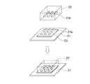
- the figure which shows the positioning process at the time of using a batch holding tray The figure which shows the example which formed the pillar in the hydrophilic film of a carrier substrate Diagram showing an example of temporarily bonding the bump electrode of the chip and the bump electrode of the carrier substrate
- Chips are stacked in the vertical direction on a support substrate constituting the three-dimensional integrated circuit.
- chips stacked on the support substrate will be described.
- An IC such as a microprocessor and a logic circuit is formed on the chip.
- TSVs Three Silicon Via
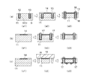
- the process of forming a TSV on a chip is roughly divided into three. There are three methods: Via First method shown in FIG. 3A, Via Last (front) method shown in FIG. 3B, and ViaVLast (back) method shown in FIG.
- the Via First method is a method in which a TSV is formed before a pre-process for manufacturing an IC.
- a trench 12 whose inner wall surface is covered with an SiO 2 film, which is an insulating film, is formed in the silicon substrate 11 from the surface side (a1). The trench 12 does not penetrate the silicon substrate 11 and stops halfway.
- a conductive plug 13 is formed by filling a conductive material such as polysilicon or tungsten (a1).
- a semiconductor element such as a CMOS or an integrated circuit 14 is formed on or inside the silicon substrate 11 (a2).
- the surface of the silicon substrate 11 on which the semiconductor element or the integrated circuit 14 is formed is covered with an SiO 2 film 15 as an insulating film (a2).
- the silicon substrate 11 is shaved from the back side, and the conductive plug 13 is exposed to the back side of the silicon substrate 11 (a3).
- a bump electrode 16 is formed on the surface of the silicon substrate 11 so as to be connected to the conductive plug 13 (a3).
- a semiconductor element or an integrated circuit 14 is first formed on a silicon substrate 11 (b1), and then a TSV is formed (b2, b3).
- the order in which TSVs 17 are formed is different from the Via First method.
- the TSV 17 is formed from the surface side of the silicon substrate 11 (b2). Also in this method, the silicon substrate 11 is thinly cut (b3).
- the semiconductor element or the integrated circuit 14 is first formed on the silicon substrate 11 as in the Via ⁇ ⁇ Last (front) method (c1).
- TSVs 17 are formed from the back side (c2, c3). It differs from the Via Last (front) method in that the TSV 17 is formed from the front surface side or the back surface side of the silicon substrate 11.
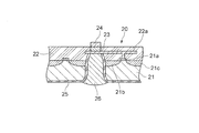
- FIG. 4 shows an example of a cross-sectional view of the chip 20.
- a gate electrode 21a is formed on the silicon substrate 21, and a source region 21b and a drain region 21c are formed on both sides of the gate electrode 21a.
- An insulating layer 22 made of SiO 2 is formed on the silicon substrate 21 so as to bury the gate electrode 21a.
- a wiring layer made of nickel or the like and a wiring layer 24 (bump electrode) made of gold or the like are formed on the surface layer portion of the insulating layer 22, a wiring layer made of nickel or the like and a wiring layer 24 (bump electrode) made of gold or the like are formed.
- An additional wiring layer 23 made of aluminum or the like is embedded in the insulating layer 22, and the gate electrode 21 a and the wiring layers 23 and 24 are electrically connected.
- vias reaching the additional wiring layer 22a are formed in the silicon substrate 21 and the insulating layer 22, and an insulating film 25 made of an SiO 2 film is formed so as to cover the side wall of the via. Then, a conductive plug 26 that is electrically connected to the additional wiring layer 22a through the insulating film 25 is formed.
- the size of the chip 20 used in the three-dimensional integrated circuit varies depending on applications such as CMOS and memory, but is, for example, 5 mm ⁇ 5 mm, 10 mm ⁇ 10 mm, or the like.
- the thickness of the chip is, for example, 20 ⁇ m to 100 ⁇ m.
- the hole diameter of TSV is, for example, 0.5 ⁇ m to 100 ⁇ m.
- FIG. 5 shows a perspective view of a carrier substrate 31 as a transfer substrate to which a large number of chips 20 are temporarily bonded.
- a large number of chips 20 are positioned and temporarily bonded to the carrier substrate 31 and then transferred to the support substrate.
- One chip 20 is temporarily bonded to one temporary bonding region 31a.
- a semiconductor wafer such as silicon, a glass substrate, or the like is used.
- An insulator or a conductor can be used as long as it has rigidity capable of holding a large number of chips 20.
- the temporary adhesion region 31a is formed in a rectangular shape.
- the size and shape of the temporary bonding region 31a substantially match the size and shape of the chip 20 temporarily bonded thereon.
- the temporary adhesion region 31a is defined by a hydrophilic film having hydrophilicity.
- the hydrophilic film is formed of, for example, SiO 2 , Si 3 N 4 , a two-layer film of aluminum and alumina (Al / Al 2 O 3 ), a two-layer film of tantalum and tantalum oxide (Ta / Ta 2 O 5 ), etc. can do.
- the periphery of the temporary adhesion region 31a is surrounded by a lattice-like hydrophobic film or hydrophobic material 31b.
- the material of the hydrophobic film or the hydrophobic material 31b include materials having a property of repelling water, such as single crystal silicon, polycrystalline silicon, amorphous silicon, fluorine resin, silicon resin, Teflon (registered trademark) resin, polyimide resin, resist, Wax, BCB (benzocyclobutene) or the like can be used.
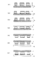
- FIG. 6 shows an example of a process chart for forming the hydrophilic film 31 a and the hydrophobic film 31 b on the carrier substrate 31.
- the SiO 2 film 33 is formed on the silicon substrate 32 (S1).
- the SiO 2 film 33 can be formed by a known method such as a thermal oxidation method, a CVD (Chemical Vapor Deposition) method, or a sputtering method.
- a photoresist 34 which is a photosensitive resin, is applied on the SiO 2 film 33 (S2).
- the silicon substrate 32 coated with the photoresist 34 is set in an exposure apparatus, and the mask pattern 35 is transferred.
- the exposed photoresist 34 is developed (S3).
- the SiO 2 film 33 is etched according to the pattern of the photoresist 34 (S4). Etching may be dry etching or wet etching. When the photoresist 34 is peeled off, the SiO 2 film 33 having a pattern corresponding to the temporary adhesion region is obtained (S5).
- a hydrophobic film 36 is formed on the surface of the SiO 2 film 33 (S6). Similar to the photoresist 34, the hydrophobic film 36 can be formed by dropping a liquid hydrophobic material onto the silicon substrate 32 and then rotating the silicon substrate 32 at a high speed using a spin coater. Next, a hard mask 37 is deposited on the hydrophobic film 36 (S7).
- the hydrophobic film 36 is melted by exposure / development processing in the same manner as the photoresist 34.
- a hard mask 37 is deposited to prevent the hydrophobic film 36 from melting.
- a photoresist 39 is applied on the hard mask 37 (S8).
- the photoresist 39 is exposed and developed using a mask pattern 41 (S9).
- the hard mask 37 is etched (S10).
- the hydrophobic film 36 on the SiO 2 film 33 is etched (S11).
- the hydrophobic film 36 may be ashed (ashed) with oxygen plasma or the like.
- the photoresist 39 is peeled off and the hard mask 37 is removed (S12).
- a frame-like hydrophobic film 31b can be formed around the rectangular hydrophilic film 31a.
- the distinction between the hydrophilic portion and the hydrophobic portion becomes clear, and the edge of the hydrophilic portion becomes clear. For this reason, the positioning of the chip 20 using the surface tension of water can also be performed with high accuracy.
- a hydrophobic film 36 is formed on the SiO 2 film 33 may be patterned only hydrophobic membrane 36. In this case, a slight step is formed between the SiO 2 film 33 and the hydrophobic film 36, and the hydrophobic film 36 is slightly higher than the SiO 2 film 33.
- the hydrophobic film 36 may be formed by lift-off. That is, after etching the SiO 2 film 33 in S4 of FIG. 6, a hydrophobic film 36 is formed on the photoresist 34 without removing the photoresist 34, and then the photoresist 34 is dissolved in a developing solution to thereby remove the photoresist 34. The resist 34 and the hydrophobic film 36 on the photoresist 34 are simultaneously removed.
- the carrier substrate 31 may be made of hydrophobic single crystal silicon, and only the hydrophilic film may be formed on the surface of the hydrophobic material.
- a contact method in which a liquid is brought into direct contact with the carrier substrate 31 or a spraying method in which water is sprayed onto the carrier substrate 31 using a nozzle is employed.
- the contact method after the carrier substrate 31 is immersed in the water stored in the container, the carrier substrate 31 is taken out from the container. The carrier substrate 31 is brought into contact with the water stored in the container with the carrier substrate 31 facing downward. Or a method of flowing water over the carrier substrate 31.
- the spraying method a method of providing a nozzle facing the carrier substrate 31 and spraying water from the nozzle toward the carrier substrate 31 is employed.
- Water may be sprayed on the entire surface of the carrier substrate 31 from a large number of nozzles, or water may be sprayed only from the nozzles arranged corresponding to the hydrophilic film 31a toward the hydrophilic film 31a. At that time, the amount of water sprayed may be controlled according to the area of the hydrophilic film 31a.
- a hydrophilic SiO 2 film 20a is formed on the back surface of the chip 20 in advance.
- the plurality of chips 20 are released onto the water droplets 40 separated for each hydrophilic film 31a (S3).
- the tip 20 released on the water droplet 40 by the surface tension of water is automatically positioned on the hydrophilic film 31a.
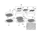
- This step may be performed for each chip 20 using, for example, a chip bonder, or a large number of chips 20 are simultaneously released onto a large number of water droplets 40 using a holding tray that holds a large number of chips 20 collectively. May be.
- FIG. 9 shows a schematic diagram when a batch holding tray is used.
- the chips 20 that are displaced in the horizontal direction with respect to the hydrophilic film 31a are automatically placed on the hydrophilic film 31a by the surface tension of water. It will be positioned at the correct position.
- the chip 20 is released onto the water droplet 40, it is not necessary to position the chip 20 at an accurate position on the hydrophilic film 31a, and rough positioning is sufficient.
- water between the back surface of the chip 20 and the hydrophilic film 31a of the carrier substrate 31 is evaporated (S4).
- Water may be evaporated in a heating or vacuum environment, or may be evaporated over a predetermined time at room temperature.
- the chip 20 and the carrier substrate 31 are bonded to each other as a solid.
- An additive for activating the SiO 2 film 20a of the chip 20 and the hydrophilic film 31a of the carrier substrate 31 may be added to the water.
- a hydrophilic group (OH group) is formed on the SiO 2 film 20a of the chip 20 and the hydrophilic film 31a (SiO 2 film) of the carrier substrate 31, and hydrofluoric acid for bonding these hydrophilic groups is added. .
- the SiO 2 film 20a of the chip 20 and the hydrophilic film 31a of the carrier substrate 31 can be activated, there is no limitation to hydrofluoric acid, and hydrochloric acid perwater mixed with ammonia, hydrochloric acid, hydrogen peroxide water and water is added. Also good.
- liquids such as glycerin, acetone, alcohol, and SOG (Spin-On-Glass) materials can be used.
- a liquid resin may be used, or a liquid mixture of a liquid resin and water may be used. However, the viscosity needs to be low enough to enable positioning.
- the carrier substrate 31 to which the plurality of chips 20 are temporarily bonded is inverted and lowered toward the support substrate 50 (S5).
- the inverted support substrate 50 may be lowered toward the carrier substrate 31 without inverting the carrier substrate 31.
- the many chips 20 temporarily bonded to the carrier substrate 31 are collectively bonded to the main bonding region 50a of the support substrate 50 at the opposite side of the surface temporarily bonded to the carrier substrate 31 (S6).
- the chip 20 is already laminated on the support substrate 50, the chip 20 is bonded to the laminated chip laminated on the support substrate 50.
- the adhesive force between the chip 20 and the support substrate 50 (or laminated chip) is adjusted to be stronger than the adhesive force between the chip 20 and the carrier substrate 31.
- a semiconductor wafer such as silicon, a glass substrate, or the like is used.
- An insulator or a conductor can be used as long as it has rigidity capable of holding a large number of chips 20.
- a SiO 2 film is formed as the main adhesion region 50a.
- the contact area between the hydrophilic film 31a (SiO 2 film) of the carrier substrate 31 and the SiO 2 film 20a of the chip 20 is made smaller than the cross-sectional area of the chip 20 in a plane parallel to the hydrophilic film 31a.
- the adhesive force between the chip 20 and the carrier substrate 31 can be weakened.
- the plurality of pillars 51 are scattered on the hydrophilic film 31 a of the carrier substrate 31, the contact area between the chip 20 and the carrier substrate 31 can be reduced.
- the pillar 51 can be formed by known lithography. Instead of the pillar 51, the contact area may be reduced by providing a minute step on the surface of the hydrophilic film 31a.
- the adhesion force of the main adhesion is made stronger than the adhesion force of the temporary adhesion. Can do.
- the surface roughness of the main adhesion region 50a of the support substrate 50 is set to, for example, 1 nm or less using a CMP (Chemical Mechanical Polishing) apparatus, the adhesion force of the main adhesion can be extremely strengthened.
- the surface roughness of the hydrophilic film 31a of the carrier substrate 31 is increased, the adhesive force of temporary bonding can be weakened.
- the SiO 2 film of the hydrophilic film 31a may be chemically roughened by etching, or may be mechanically roughened by a grindstone or the like.
- the hydrophilic film 31a of the carrier substrate 31 may be formed on a peelable sacrificial layer.
- the chip 20 When the chip 20 is peeled from the carrier substrate 31, the chip 20 may be peeled from the carrier substrate 31 with the sacrificial layer as a boundary in a state where the hydrophilic film 31 a of the carrier substrate 31 is adhered to the chip 20.
- a resin that dissolves by injecting a chemical solution or a photo-release resin can be used for the sacrificial layer.
- the electrode of the chip 20 e.g., a bump electrode
- the electrodes (for example, bump electrodes) of the support substrate 50 are bonded together, or they are used in combination.
- the adhesion force of the main adhesion between the support substrate 50 and the chip 20 can be increased.
- Examples of conductive materials for electrodes include a two-layer structure (In / Au) of indium (In) and gold (Au), a two-layer structure (Sn / Ag) of tin (Sn) and silver (Ag), and copper.
- a single layer structure of (Cu) or a single layer structure of tungsten (W) can be preferably used.
- the electrode of the chip 20 e.g., a bump electrode
- the electrode of the laminated chip e.g. bump electrode
- Electrode for example, a bump electrode of the carrier substrate 31 may be bonded together, or they may be used in combination.
- 11 and 12 show an example in which the bump electrode 20b of the chip 20 and the bump electrode 53 in the hydrophilic film 31a of the carrier substrate 31 are temporarily bonded in the temporary bonding.
- the positions of the bump electrodes 20b of the chip 20 and the bump electrodes 53 of the carrier substrate 31 are determined, and these can be temporarily bonded.
- Figure 13 shows an example of temporarily bonding the SiO 2 film of the SiO 2 film and the chip 20 of the carrier substrate 31.
- a recess 56 corresponding to the bump electrodes 20b of the chip 20 in the same manner as the supporting substrate 50 a SiO 2 film of the SiO 2 film and the tip 20 of the supporting substrate 50 can be the adhesion.
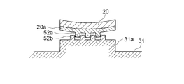
- FIG. 14 shows an example in which stoppers 52a and 52b that can mesh with the back surface of the chip 20 and the hydrophilic film 31a of the carrier substrate 31 are formed.
- the stopper 52a of the chip 20 enters the stopper 52b of the carrier substrate 31 as the water evaporates, the stoppers 52a and 52b are engaged with each other, and the chip 20 is displaced in the plane of the hydrophilic film 31a. To prevent it.
- the cross-sectional shapes of the stoppers 52a and 52b may be formed in a rectangular shape, or may be formed in a tapered shape in which the position of the chip 20 is determined as the chip 20 approaches the carrier substrate 31.
- the stoppers 52a and 52b can be formed by known lithography.
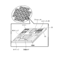
- FIG. 15 shows an example in which a single layer of chips 20 is arranged on the support substrate 50.
- Each chip 20 has functions such as a processor, logic, and memory.
- the plurality of chips 20 are planarly arranged on the support substrate 50, but are not stacked in the vertical direction.
- one layer of chips 20 may be arranged on the support substrate 50.
- this invention is not limited to the said embodiment, In the range which does not change the summary of this invention, it can change variously.
- SiO 2 film by lithography on the surface of the carrier substrate may be formed SiO 2 film by the silicon substrate to oxidation.
- oxidation treatment H 2 O 2 treatment or oxidation treatment using ozone can be used.
- the SiO 2 film may be formed by natural oxidation without oxidizing the silicon substrate.
- the chip After positioning and temporarily bonding the chip to the temporary bonding region of the carrier substrate, the chip may be pressed against the carrier substrate using a pressing plate. If the pressing plate is used, the entire surface of the chip can be temporarily bonded to the carrier substrate even when the chip is warped.
- an electrically insulating adhesive may be disposed between the chip and the laminated chip, and the chip and the laminated chip may be bonded by this electrically insulating adhesive.
- the bump electrode may be formed on the chip after the chip is attached to the support substrate, or the chip on which the bump electrode has been previously formed may be laminated on the support substrate.
Landscapes
- Container, Conveyance, Adherence, Positioning, Of Wafer (AREA)
Abstract
Description
疎水膜36は、酸素プラズマ等により灰化処理(アッシング)されてもよい。最後にフォトレジスト39を剥離し、ハードマスク37を除去する(S12)。
20a…チップのSiO2膜
31…キャリア基板(転写用基板)
31a…親水膜(仮接着領域)
31b…疎水膜
40…水滴
50…支持基板
50a…本接着領域
51…ピラー
52a,52b…ストッパ
Claims (11)
- 支持基板にチップを積層してなる三次元集積回路の製造方法において、
転写用基板に形成された複数の仮接着領域に液体を塗布する工程と、
前記複数の仮接着領域毎に分離された複数の液滴上に複数のチップを解放し、液体の表面張力を利用して各チップを各仮接着領域に位置決めする工程と、
前記各チップと前記各仮接着領域との間の液体を蒸発させることによって、前記各チップを前記各仮接着領域に仮接着する工程と、
前記複数のチップが仮接着された前記転写用基板を支持基板に接近させ、前記複数のチップの、前記転写用基板に仮接着された面とは反対側を、前記支持基板の複数の本接着領域又は複数の本接着領域に積層された複数の積層チップに、前記各チップと前記支持基板又は前記支持基板上の各積層チップとの接着力が前記各チップと前記転写用基板との接着力よりも強くなるように一括して本接着する工程と、
前記支持基板から前記転写用基板を離間させることによって、前記複数のチップを前記支持基板又は前記支持基板上の前記複数の積層チップに接着させたまま、前記複数のチップを前記転写用基板から剥離する工程と、を備える三次元集積回路の製造方法。 - 前記液体には、前記液体を蒸発させたとき、前記各チップを前記各仮接着領域に仮接着させる添加剤が添加されることを特徴とする請求項1に記載の三次元集積回路の製造方法。
- 前記転写用基板の前記各仮接着領域、及び前記各チップの前記転写用基板に仮接着される面には、SiO2膜が形成され、
前記添加剤は、前記SiO2膜同士を接着させることを特徴とする請求項2に記載の三次元集積回路の製造方法。 - 前記転写用基板の前記各仮接着領域の前記SiO2膜と前記各チップの前記SiO2膜との接触面積が、前記各仮接着領域と平行な平面における前記各チップの断面積よりも小さいことを特徴とする請求項3に記載の三次元集積回路の製造方法。
- 前記支持基板のSiO2膜の表面粗さが前記転写用基板の前記各仮接着領域のSiO2膜の表面粗さよりも小さいことを特徴とする請求項3又は4に記載の三次元集積回路の製造方法。
- 前記転写用基板の前記各仮接着領域の前記SiO2膜は、剥離可能な犠牲層上に形成され、
前記複数のチップを前記転写用基板から剥離するとき、前記転写用基板の前記各仮接着領域の前記SiO2膜を前記各チップに接着させた状態で、前記複数のチップを前記転写用基板から剥離することを特徴とする請求項3に記載の三次元集積回路の製造方法。 - 前記転写用基板には、前記仮接着領域を画定し、前記液体に対して親液性を有する親液性膜が形成されると共に、前記仮接着領域を囲み、前記液体に対して疎液性を有する疎液性膜が形成されることを特徴とする請求項1に記載の三次元集積回路の製造方法。
- 前記転写用基板の前記複数の仮接着領域のうち、相対的に面積が小さい仮接着領域には、相対的に少量の液滴が塗布され、相対的に面積が大きい仮接着領域には、相対的に多量の液滴が塗布されることを特徴とする請求項1に記載の三次元集積回路の製造方法。
- 前記転写用基板に形成された複数の仮接着領域に液体を塗布する工程において、
前記転写用基板に液体を直接接触させるか、又はノズルを用いて前記転写用基板に液体を噴霧することによって、前記複数の仮接着領域に前記複数の液滴を塗布することを特徴とする請求項1に記載の三次元集積回路の製造方法。 - 前記転写用基板の前記仮接着領域及び前記各チップには、互いに噛み合うことができるストッパが形成され、
前記ストッパは、前記液体の表面張力を利用して各チップを各仮接着領域に位置決めするとき、互いに噛み合って前記各チップが前記各仮接着領域に対して前記各仮接着領域の平面内で位置ずれするのを防止することを特徴とする請求項1に記載の三次元集積回路の製造方法。 - 支持基板にチップを積層してなる三次元集積回路の製造装置において、
複数の仮接着領域が形成される転写用基板と、
転写用基板に形成された複数の仮接着領域に液体を塗布する液体塗布手段と、を備え、
前記複数の仮接着領域毎に分離された複数の液滴上に複数のチップを解放し、液体の表面張力を利用して各チップを各仮接着領域に位置決めし、
前記各チップと前記各仮接着領域との間の液体を蒸発させることによって、前記各チップを前記各仮接着領域に仮接着し、
前記複数のチップが仮接着された前記転写用基板を支持基板に接近させ、前記複数のチップの、前記転写用基板に仮接着された面とは反対側を、前記支持基板の複数の本接着領域又は複数の本接着領域に積層された複数の積層チップに、前記各チップと前記支持基板又は前記支持基板上の各積層チップとの接着力が前記各チップと前記転写用基板との接着力よりも強くなるように一括して本接着し、
前記支持基板から前記転写用基板を離間させることによって、前記複数のチップを前記支持基板又は前記支持基板上の前記複数の積層チップに接着させたまま、前記複数のチップを前記転写用基板から剥離する三次元集積回路の製造装置。
Priority Applications (2)
| Application Number | Priority Date | Filing Date | Title |
|---|---|---|---|
| US13/258,664 US8349652B2 (en) | 2009-03-23 | 2010-03-10 | Method and apparatus for manufacturing three-dimensional integrated circuit |
| KR1020117022030A KR101276625B1 (ko) | 2009-03-23 | 2010-03-10 | 삼차원 집적 회로의 제조 방법 및 장치 |
Applications Claiming Priority (2)
| Application Number | Priority Date | Filing Date | Title |
|---|---|---|---|
| JP2009070769A JP5389490B2 (ja) | 2009-03-23 | 2009-03-23 | 三次元集積回路の製造方法及び装置 |
| JP2009-070769 | 2009-03-23 |
Publications (1)
| Publication Number | Publication Date |
|---|---|
| WO2010110070A1 true WO2010110070A1 (ja) | 2010-09-30 |
Family
ID=42780763
Family Applications (1)
| Application Number | Title | Priority Date | Filing Date |
|---|---|---|---|
| PCT/JP2010/054031 Ceased WO2010110070A1 (ja) | 2009-03-23 | 2010-03-10 | 三次元集積回路の製造方法及び装置 |
Country Status (5)
| Country | Link |
|---|---|
| US (1) | US8349652B2 (ja) |
| JP (1) | JP5389490B2 (ja) |
| KR (1) | KR101276625B1 (ja) |
| TW (1) | TWI433294B (ja) |
| WO (1) | WO2010110070A1 (ja) |
Families Citing this family (20)
| Publication number | Priority date | Publication date | Assignee | Title |
|---|---|---|---|---|
| US9343436B2 (en) * | 2010-09-09 | 2016-05-17 | Taiwan Semiconductor Manufacturing Company, Ltd. | Stacked package and method of manufacturing the same |
| JP2013182973A (ja) * | 2012-03-01 | 2013-09-12 | Tokyo Electron Ltd | 基板の接合方法及び半導体装置 |
| EP2701189B1 (en) * | 2012-08-24 | 2016-01-20 | Imec | Substrate, fabrication method of such a substrate, method of self-assembly of such substrates and device obtained thereof |
| JP6027828B2 (ja) * | 2012-09-14 | 2016-11-16 | 国立大学法人東北大学 | 素子の実装方法および光モジュールの製造方法 |
| NL2009757C2 (en) * | 2012-11-05 | 2014-05-08 | Micronit Microfluidics Bv | Method for forming an electrically conductive via in a substrate. |
| JP6306568B2 (ja) | 2013-03-07 | 2018-04-04 | 東北マイクロテック株式会社 | 積層体及びその製造方法 |
| JP6278760B2 (ja) * | 2014-03-11 | 2018-02-14 | 株式会社ディスコ | チップ整列方法 |
| JP6225771B2 (ja) * | 2014-03-17 | 2017-11-08 | 株式会社デンソー | 半導体装置およびその製造方法 |
| KR101596131B1 (ko) * | 2014-04-25 | 2016-02-22 | 한국과학기술원 | 소수성 표면을 이용한 칩 패키징 방법 및 칩 패키지 |
| JP5882510B2 (ja) * | 2014-06-30 | 2016-03-09 | 太陽インキ製造株式会社 | 感光性ドライフィルムおよびそれを用いたプリント配線板の製造方法 |
| WO2017159401A1 (ja) * | 2016-03-17 | 2017-09-21 | 東京エレクトロン株式会社 | 液体を用いて基板に対するチップ部品のアライメントを行う方法 |
| KR20230151553A (ko) | 2016-06-27 | 2023-11-01 | 애플 인크. | 조합된 높은 밀도, 낮은 대역폭 및 낮은 밀도, 높은 대역폭 메모리들을 갖는 메모리 시스템 |
| JP6842660B2 (ja) * | 2017-02-10 | 2021-03-17 | 国立大学法人東北大学 | 基材、塗布方法及び塗布装置 |
| FR3063832B1 (fr) | 2017-03-08 | 2019-03-22 | Commissariat A L'energie Atomique Et Aux Energies Alternatives | Procede d'auto-assemblage de composants microelectroniques |
| CN108122814B (zh) * | 2017-10-27 | 2021-04-23 | 江西乾照光电有限公司 | 一种led芯片中led芯粒的分选转移方法 |
| JP7199307B2 (ja) * | 2019-05-24 | 2023-01-05 | 株式会社ディスコ | 移設方法 |
| CN110752145B (zh) * | 2019-10-28 | 2022-03-01 | 清华大学 | 基于液体毛细力和表面张力的转印方法和转印头 |
| TWI874441B (zh) * | 2019-10-29 | 2025-03-01 | 日商東京威力科創股份有限公司 | 附有晶片之基板的製造方法及基板處理裝置 |
| CN112781421B (zh) * | 2021-02-04 | 2022-09-27 | 广东机电职业技术学院 | 一种具有仿生吸液芯的超薄热管 |
| JP2024080246A (ja) * | 2022-12-02 | 2024-06-13 | タツモ株式会社 | 積層デバイスの製造方法 |
Citations (4)
| Publication number | Priority date | Publication date | Assignee | Title |
|---|---|---|---|---|
| JPH06163634A (ja) * | 1991-09-24 | 1994-06-10 | Nec Corp | フリップチップ型半導体装置の実装方法 |
| JP2001332710A (ja) * | 2000-05-24 | 2001-11-30 | Yotaro Hatamura | 装置及び装置の製造方法 |
| JP2004537158A (ja) * | 2001-02-08 | 2004-12-09 | インターナショナル・ビジネス・マシーンズ・コーポレーション | チップ転写方法および該装置 |
| WO2006077739A1 (ja) * | 2004-12-28 | 2006-07-27 | Mitsumasa Koyanagi | 自己組織化機能を用いた集積回路装置の製造方法及び製造装置 |
Family Cites Families (5)
| Publication number | Priority date | Publication date | Assignee | Title |
|---|---|---|---|---|
| US6790691B2 (en) * | 2001-06-29 | 2004-09-14 | Xanoptix, Inc. | Opto-electronic device integration |
| JP2006066841A (ja) * | 2004-08-30 | 2006-03-09 | Epson Toyocom Corp | シート状ウェハのダイシング及び梱包方法、ウェハの梱包物、剥離治具 |
| US7400037B2 (en) * | 2004-12-30 | 2008-07-15 | Advanced Chip Engineering Tachnology Inc. | Packaging structure with coplanar filling paste and dice and with patterned glue for WL-CSP |
| JP2009130269A (ja) * | 2007-11-27 | 2009-06-11 | Nec Electronics Corp | 半導体製造装置および半導体装置の製造方法 |
| US8378498B2 (en) * | 2010-09-09 | 2013-02-19 | International Business Machines Corporation | Chip assembly with a coreless substrate employing a patterned adhesive layer |
-
2009
- 2009-03-23 JP JP2009070769A patent/JP5389490B2/ja active Active
-
2010
- 2010-03-10 KR KR1020117022030A patent/KR101276625B1/ko active Active
- 2010-03-10 WO PCT/JP2010/054031 patent/WO2010110070A1/ja not_active Ceased
- 2010-03-10 US US13/258,664 patent/US8349652B2/en active Active
- 2010-03-10 TW TW099106838A patent/TWI433294B/zh active
Patent Citations (4)
| Publication number | Priority date | Publication date | Assignee | Title |
|---|---|---|---|---|
| JPH06163634A (ja) * | 1991-09-24 | 1994-06-10 | Nec Corp | フリップチップ型半導体装置の実装方法 |
| JP2001332710A (ja) * | 2000-05-24 | 2001-11-30 | Yotaro Hatamura | 装置及び装置の製造方法 |
| JP2004537158A (ja) * | 2001-02-08 | 2004-12-09 | インターナショナル・ビジネス・マシーンズ・コーポレーション | チップ転写方法および該装置 |
| WO2006077739A1 (ja) * | 2004-12-28 | 2006-07-27 | Mitsumasa Koyanagi | 自己組織化機能を用いた集積回路装置の製造方法及び製造装置 |
Also Published As
| Publication number | Publication date |
|---|---|
| TWI433294B (zh) | 2014-04-01 |
| US20120021563A1 (en) | 2012-01-26 |
| TW201108386A (en) | 2011-03-01 |
| KR101276625B1 (ko) | 2013-06-19 |
| US8349652B2 (en) | 2013-01-08 |
| JP2010225803A (ja) | 2010-10-07 |
| JP5389490B2 (ja) | 2014-01-15 |
| KR20110129415A (ko) | 2011-12-01 |
Similar Documents
| Publication | Publication Date | Title |
|---|---|---|
| JP5389490B2 (ja) | 三次元集積回路の製造方法及び装置 | |
| US20220208723A1 (en) | Directly bonded structures | |
| US8283208B2 (en) | Method and apparatus for fabricating integrated circuit device using self-organizing function | |
| CN103426732B (zh) | 低温晶圆键合的方法及通过该方法形成的结构 | |
| TWI866439B (zh) | 三維封裝結構及其製備方法 | |
| TWI525720B (zh) | 半導體裝置及其形成方法 | |
| US10276540B2 (en) | Chip packaging method and chip packaging structure | |
| US10622327B2 (en) | Method for manufacturing semiconductor structure | |
| CN105502280B (zh) | Mems器件的形成方法 | |
| US20070126085A1 (en) | Semiconductor device and method of manufacturing the same | |
| KR20190024570A (ko) | 반도체 패키지 내의 도전성 비아 및 그 형성 방법 | |
| TW201719480A (zh) | 指紋感測器裝置與方法 | |
| JP2015520525A (ja) | パターン未形成接着層を利用した3次元電子回路パッケージ | |
| CN105374731A (zh) | 封装方法 | |
| CN105225973A (zh) | 封装方法 | |
| JP2010245452A (ja) | 一括保持トレイ及び三次元集積回路製造装置 | |
| US20210202338A1 (en) | Wafer-level sip module structure and method for preparing the same | |
| CN105097565B (zh) | 封装结构的形成方法 | |
| TWI590416B (zh) | 封裝及形成封裝的方法 | |
| WO2024021356A1 (zh) | 高深宽比tsv电联通结构及其制造方法 | |
| CN105097728B (zh) | 封装结构 | |
| CN113078133A (zh) | 多层布线转接板及其制备方法 | |
| TW202510288A (zh) | 形貌封裝中的直接混合接合 | |
| CN116918057A (zh) | 直接接合结构 |
Legal Events
| Date | Code | Title | Description |
|---|---|---|---|
| 121 | Ep: the epo has been informed by wipo that ep was designated in this application |
Ref document number: 10755870 Country of ref document: EP Kind code of ref document: A1 |
|
| ENP | Entry into the national phase |
Ref document number: 20117022030 Country of ref document: KR Kind code of ref document: A |
|
| NENP | Non-entry into the national phase |
Ref country code: DE |
|
| WWE | Wipo information: entry into national phase |
Ref document number: 13258664 Country of ref document: US |
|
| 122 | Ep: pct application non-entry in european phase |
Ref document number: 10755870 Country of ref document: EP Kind code of ref document: A1 |