WO2010103940A1 - 樹脂配線基板 - Google Patents
樹脂配線基板 Download PDFInfo
- Publication number
- WO2010103940A1 WO2010103940A1 PCT/JP2010/053117 JP2010053117W WO2010103940A1 WO 2010103940 A1 WO2010103940 A1 WO 2010103940A1 JP 2010053117 W JP2010053117 W JP 2010053117W WO 2010103940 A1 WO2010103940 A1 WO 2010103940A1
- Authority
- WO
- WIPO (PCT)
- Prior art keywords
- layer
- conductor layer
- resin
- conductor
- wiring board
- Prior art date
- Legal status (The legal status is an assumption and is not a legal conclusion. Google has not performed a legal analysis and makes no representation as to the accuracy of the status listed.)
- Ceased
Links
Images



Classifications
-
- H—ELECTRICITY
- H05—ELECTRIC TECHNIQUES NOT OTHERWISE PROVIDED FOR
- H05K—PRINTED CIRCUITS; CASINGS OR CONSTRUCTIONAL DETAILS OF ELECTRIC APPARATUS; MANUFACTURE OF ASSEMBLAGES OF ELECTRICAL COMPONENTS
- H05K1/00—Printed circuits
- H05K1/02—Details
- H05K1/0271—Arrangements for reducing stress or warp in rigid printed circuit boards, e.g. caused by loads, vibrations or differences in thermal expansion
-
- H—ELECTRICITY
- H05—ELECTRIC TECHNIQUES NOT OTHERWISE PROVIDED FOR
- H05K—PRINTED CIRCUITS; CASINGS OR CONSTRUCTIONAL DETAILS OF ELECTRIC APPARATUS; MANUFACTURE OF ASSEMBLAGES OF ELECTRICAL COMPONENTS
- H05K1/00—Printed circuits
- H05K1/02—Details
- H05K1/09—Use of materials for the conductive, e.g. metallic pattern
-
- H—ELECTRICITY
- H05—ELECTRIC TECHNIQUES NOT OTHERWISE PROVIDED FOR
- H05K—PRINTED CIRCUITS; CASINGS OR CONSTRUCTIONAL DETAILS OF ELECTRIC APPARATUS; MANUFACTURE OF ASSEMBLAGES OF ELECTRICAL COMPONENTS
- H05K2201/00—Indexing scheme relating to printed circuits covered by H05K1/00
- H05K2201/03—Conductive materials
- H05K2201/0332—Structure of the conductor
- H05K2201/0335—Layered conductors or foils
- H05K2201/0338—Layered conductor, e.g. layered metal substrate, layered finish layer or layered thin film adhesion layer
-
- H—ELECTRICITY
- H05—ELECTRIC TECHNIQUES NOT OTHERWISE PROVIDED FOR
- H05K—PRINTED CIRCUITS; CASINGS OR CONSTRUCTIONAL DETAILS OF ELECTRIC APPARATUS; MANUFACTURE OF ASSEMBLAGES OF ELECTRICAL COMPONENTS
- H05K2201/00—Indexing scheme relating to printed circuits covered by H05K1/00
- H05K2201/06—Thermal details
- H05K2201/068—Thermal details wherein the coefficient of thermal expansion is important
-
- H—ELECTRICITY
- H05—ELECTRIC TECHNIQUES NOT OTHERWISE PROVIDED FOR
- H05K—PRINTED CIRCUITS; CASINGS OR CONSTRUCTIONAL DETAILS OF ELECTRIC APPARATUS; MANUFACTURE OF ASSEMBLAGES OF ELECTRICAL COMPONENTS
- H05K3/00—Apparatus or processes for manufacturing printed circuits
- H05K3/46—Manufacturing multilayer circuits
- H05K3/4611—Manufacturing multilayer circuits by laminating two or more circuit boards
- H05K3/4614—Manufacturing multilayer circuits by laminating two or more circuit boards the electrical connections between the circuit boards being made during lamination
- H05K3/4617—Manufacturing multilayer circuits by laminating two or more circuit boards the electrical connections between the circuit boards being made during lamination characterized by laminating only or mainly similar single-sided circuit boards
-
- H—ELECTRICITY
- H05—ELECTRIC TECHNIQUES NOT OTHERWISE PROVIDED FOR
- H05K—PRINTED CIRCUITS; CASINGS OR CONSTRUCTIONAL DETAILS OF ELECTRIC APPARATUS; MANUFACTURE OF ASSEMBLAGES OF ELECTRICAL COMPONENTS
- H05K3/00—Apparatus or processes for manufacturing printed circuits
- H05K3/46—Manufacturing multilayer circuits
- H05K3/4611—Manufacturing multilayer circuits by laminating two or more circuit boards
- H05K3/4626—Manufacturing multilayer circuits by laminating two or more circuit boards characterised by the insulating layers or materials
- H05K3/4632—Manufacturing multilayer circuits by laminating two or more circuit boards characterised by the insulating layers or materials laminating thermoplastic or uncured resin sheets comprising printed circuits without added adhesive materials between the sheets
Definitions
- the alloy is formed by a step of laminating the conductor layer and the resin layer.
- a conductor layer is a thing which has Cu as a main component, as a 2nd metal with a larger thermal expansion coefficient than a 1st conductor layer which comprises a 2nd conductor layer, Cr, Zn, Al, Sn, Ni
- a 2nd metal with a larger thermal expansion coefficient than a 1st conductor layer which comprises a 2nd conductor layer, Cr, Zn, Al, Sn, Ni
- thermoplastic resin layer 1 base material layer A
- a conductive paste 4a containing Ag particles as a main component is filled in the through-holes 3 for via holes.
Landscapes
- Engineering & Computer Science (AREA)
- Microelectronics & Electronic Packaging (AREA)
- Production Of Multi-Layered Print Wiring Board (AREA)
- Parts Printed On Printed Circuit Boards (AREA)
Abstract
Description
樹脂層と導体層とが積層された構造を有する樹脂配線基板において、
前記導体層は、第1の金属からなる第1導体層と、前記樹脂層と前記第1導体層との間に位置するように配設された、前記第1の金属よりも熱膨張係数の大きい第2の金属からなる第2導体層と
を備えていることを特徴としている。
(b)前記第1導体層と前記第2導体層の間に、第1導体層を構成する第1の金属と、第2導体層を構成する第2の金属との合金からなる合金層が形成されていること
が望ましい。
そして、その場合、別途、第1の金属と第2の金属を合金させるプロセスを必要とすることなく、第1の金属と第2の金属とを合金化させることが可能で、生産性を低下させることがない。
また、第2導体層を構成する第2の金属が、積層、圧着の工程で溶融しない高融点の金属からなるものである場合、積層、圧着の工程の終了後に、第1導体層と第2導体層の間に、第1導体層を構成する第1の金属と、第2導体層を構成する第2の金属との合金層(すなわち、固相拡散による拡散層)が形成される可能性が高くなる。
この実施例1では、熱膨張係数(線膨張率)が約18(平面方向)、約60(厚み方向)(10-6/℃)となるような熱可塑性樹脂を選択した。
なお、樹脂層1を構成する樹脂は必ずしも、熱可塑性樹脂に限られるものではなく、熱硬化性樹脂を用いることも可能である。
なお、Cuの熱膨張係数(線膨張率)は、約16(10-6/℃)であり、Alの熱膨張係数(線膨張率)は、約23(10-6/℃)である。
したがって、熱可塑性樹脂層1と導体層2との間の熱膨張係数の差から生じる応力を緩和して、反りや歪みの少ない多層樹脂配線基板10を得ることが可能になる。
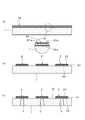
(1)まず、図2(a)に示すように、液晶ポリマー(LCP)や、ポリエーテルエーテルケトン(PEEK)などに代表される250℃以上の融点を持つ熱可塑性樹脂からなる絶縁層である熱可塑性樹脂層1に、第1導体層21となるCu箔(第1導体層用の金属層)21aと、その表裏両主面の全面にめっきにより形成された、第2導体層22となる、Cuよりも熱膨張係数の大きい金属であるAlからなる被覆層(第2導体層用の金属層)22aとを有する、パターニング前の導体層(金属箔)2aを貼り付けたシートを用意する。
なお、第2導体層用の金属層22aは、めっき以外にスパッタなどの薄膜形成方法によっても形成することが可能である。
なお、導体層(導体パターン)2を形成するにあたっては、例えば、金属箔2aの表面に、所定のレジストパターンを形成し、エッチング液に浸漬してエッチングを行った後、レジストパターンを除去することにより、図2(b)に示すような所望の導体パターン2を形成することができる。
ただし、予めパターン化した金属箔を張り付けるようにすることも可能である。
その結果、熱可塑性樹脂層1と導体層2との間の、熱膨張係数の差から生じる応力を緩和して、反りや歪みの少ない多層樹脂配線基板10を効率よく製造することが可能になる。
2 導体層(導体パターン)
2a パターニング前の導体層
3 ビアホール用貫通孔
4 ビアホール導体
4a 導電性ペースト
10 樹脂配線基板(多層樹脂配線基板)
21 第1導体層(Cu箔)
21a 第1導体層用の金属層
22 第2導体層(Al層)
22a 第2導体層用の金属層
23 合金層(固相拡散層)
A 基材層
Claims (9)
- 樹脂層と導体層とが積層された構造を有する樹脂配線基板において、
前記導体層は、第1の金属からなる第1導体層と、前記樹脂層と前記第1導体層との間に位置するように配設された、前記第1の金属よりも熱膨張係数の大きい第2の金属からなる第2導体層と
を備えていることを特徴とする樹脂配線基板。 - 前記第2導体層は、前記樹脂層と接するように配設されていることを特徴とする請求項1に記載の樹脂配線基板。
- 前記第2導体層は、前記第1導体層と接するように配設されていることを特徴とする請求項1または2に記載の樹脂配線基板。
- 前記第2導体層は、前記導体層と前記樹脂層との界面全体に存在することを特徴とする請求項1~3のいずれかに記載の樹脂配線基板。
- (a)前記第2導体層は、第1導体層を構成する第1の金属を含む合金からなる層であること、または
(b)前記第1導体層と前記第2導体層の間に、第1導体層を構成する第1の金属と、第2導体層を構成する第2の金属との合金からなる合金層が形成されていること
を特徴とする請求項1~4のいずれかに記載の樹脂配線基板。 - 前記合金は、前記導体層と前記樹脂層とを積層する工程で形成されるものであることを特徴とする請求項5に記載の樹脂配線基板。
- 前記樹脂層は、熱可塑性樹脂よりなるものであることを特徴とする請求項1~6のいずれかに記載の樹脂配線基板。
- 前記第2導体層は、熱膨張係数が前記樹脂層より小さいものであることを特徴とする請求項1~7のいずれかに記載の樹脂配線基板。
- 前記第1導体層を構成する前記第1の金属は、Cuを主成分とするものであることを特徴とする請求項1~8のいずれかに記載の樹脂配線基板。
Priority Applications (3)
| Application Number | Priority Date | Filing Date | Title |
|---|---|---|---|
| JP2011503766A JP5287976B2 (ja) | 2009-03-09 | 2010-02-26 | 樹脂配線基板 |
| CN201080012041.2A CN102349359B (zh) | 2009-03-09 | 2010-02-26 | 树脂布线基板 |
| US13/227,523 US8389866B2 (en) | 2009-03-09 | 2011-09-08 | Resin circuit board |
Applications Claiming Priority (2)
| Application Number | Priority Date | Filing Date | Title |
|---|---|---|---|
| JP2009054874 | 2009-03-09 | ||
| JP2009-054874 | 2009-03-09 |
Related Child Applications (1)
| Application Number | Title | Priority Date | Filing Date |
|---|---|---|---|
| US13/227,523 Continuation US8389866B2 (en) | 2009-03-09 | 2011-09-08 | Resin circuit board |
Publications (1)
| Publication Number | Publication Date |
|---|---|
| WO2010103940A1 true WO2010103940A1 (ja) | 2010-09-16 |
Family
ID=42728230
Family Applications (1)
| Application Number | Title | Priority Date | Filing Date |
|---|---|---|---|
| PCT/JP2010/053117 Ceased WO2010103940A1 (ja) | 2009-03-09 | 2010-02-26 | 樹脂配線基板 |
Country Status (4)
| Country | Link |
|---|---|
| US (1) | US8389866B2 (ja) |
| JP (1) | JP5287976B2 (ja) |
| CN (1) | CN102349359B (ja) |
| WO (1) | WO2010103940A1 (ja) |
Cited By (6)
| Publication number | Priority date | Publication date | Assignee | Title |
|---|---|---|---|---|
| JP2013229971A (ja) * | 2012-04-24 | 2013-11-07 | Denso Corp | 熱電子発電素子 |
| JP2015080368A (ja) * | 2013-10-18 | 2015-04-23 | 株式会社デンソー | 回転電機の固定子及びその固定子を備えた回転電機 |
| JP2019029637A (ja) * | 2017-07-28 | 2019-02-21 | サムソン エレクトロ−メカニックス カンパニーリミテッド. | プリント回路基板 |
| JPWO2021182158A1 (ja) * | 2020-03-11 | 2021-09-16 | ||
| JPWO2021182157A1 (ja) * | 2020-03-11 | 2021-09-16 | ||
| JP2023049122A (ja) * | 2021-09-29 | 2023-04-10 | 信越ポリマー株式会社 | プリント配線板用のpaek樹脂基材、及び該paek樹脂基材を有する金属張積層板 |
Families Citing this family (8)
| Publication number | Priority date | Publication date | Assignee | Title |
|---|---|---|---|---|
| KR20140030918A (ko) * | 2012-09-04 | 2014-03-12 | 삼성전기주식회사 | 인쇄회로기판 |
| JP5513694B1 (ja) * | 2012-09-07 | 2014-06-04 | 日本特殊陶業株式会社 | 配線基板およびその製造方法 |
| CN103841771A (zh) * | 2012-11-26 | 2014-06-04 | 北大方正集团有限公司 | 组合印制电路板和印制电路板的制造方法以及印制电路板 |
| DE102014109183A1 (de) * | 2014-07-01 | 2016-01-21 | Infineon Technologies Ag | Verfahren zur Herstellung eines Schaltungsträgers und zum Verbinden eines elektrischen Leiters mit einer Metallisierungsschicht eines Schaltungsträgers |
| KR102427974B1 (ko) * | 2018-03-13 | 2022-08-02 | 엔지케이 인슐레이터 엘티디 | 웨이퍼 유지대 |
| US11357111B2 (en) * | 2018-08-27 | 2022-06-07 | Tactotek Oy | Method for manufacturing a multilayer structure with embedded functionalities and related multilayer structure |
| WO2021145662A1 (ko) * | 2020-01-14 | 2021-07-22 | 엘지이노텍 주식회사 | 회로 기판 |
| CN119450902A (zh) * | 2023-08-01 | 2025-02-14 | 同欣电子工业股份有限公司 | 包含不同热膨胀系数金属材料的电路板结构及其制造方法 |
Citations (2)
| Publication number | Priority date | Publication date | Assignee | Title |
|---|---|---|---|---|
| JP2003332749A (ja) * | 2002-01-11 | 2003-11-21 | Denso Corp | 受動素子内蔵基板、その製造方法及び受動素子内蔵基板形成用素板 |
| JP2003347742A (ja) * | 2002-05-27 | 2003-12-05 | Hitachi Ltd | 多層回路基板とその製造法及び多層回路用基板並びに電子装置 |
Family Cites Families (4)
| Publication number | Priority date | Publication date | Assignee | Title |
|---|---|---|---|---|
| JPH11354684A (ja) * | 1998-06-09 | 1999-12-24 | Nitto Denko Corp | 低熱膨張配線基板および多層配線基板 |
| JP3142259B2 (ja) | 1998-11-30 | 2001-03-07 | 三井金属鉱業株式会社 | 耐薬品性および耐熱性に優れたプリント配線板用銅箔およびその製造方法 |
| US6296949B1 (en) * | 1999-09-16 | 2001-10-02 | Ga-Tek Inc. | Copper coated polyimide with metallic protective layer |
| CN102342186A (zh) * | 2009-03-09 | 2012-02-01 | 株式会社村田制作所 | 柔性基板 |
-
2010
- 2010-02-26 JP JP2011503766A patent/JP5287976B2/ja active Active
- 2010-02-26 WO PCT/JP2010/053117 patent/WO2010103940A1/ja not_active Ceased
- 2010-02-26 CN CN201080012041.2A patent/CN102349359B/zh active Active
-
2011
- 2011-09-08 US US13/227,523 patent/US8389866B2/en active Active
Patent Citations (2)
| Publication number | Priority date | Publication date | Assignee | Title |
|---|---|---|---|---|
| JP2003332749A (ja) * | 2002-01-11 | 2003-11-21 | Denso Corp | 受動素子内蔵基板、その製造方法及び受動素子内蔵基板形成用素板 |
| JP2003347742A (ja) * | 2002-05-27 | 2003-12-05 | Hitachi Ltd | 多層回路基板とその製造法及び多層回路用基板並びに電子装置 |
Cited By (12)
| Publication number | Priority date | Publication date | Assignee | Title |
|---|---|---|---|---|
| JP2013229971A (ja) * | 2012-04-24 | 2013-11-07 | Denso Corp | 熱電子発電素子 |
| JP2015080368A (ja) * | 2013-10-18 | 2015-04-23 | 株式会社デンソー | 回転電機の固定子及びその固定子を備えた回転電機 |
| JP2019029637A (ja) * | 2017-07-28 | 2019-02-21 | サムソン エレクトロ−メカニックス カンパニーリミテッド. | プリント回路基板 |
| JP7073602B2 (ja) | 2017-07-28 | 2022-05-24 | サムソン エレクトロ-メカニックス カンパニーリミテッド. | プリント回路基板 |
| JPWO2021182158A1 (ja) * | 2020-03-11 | 2021-09-16 | ||
| JPWO2021182157A1 (ja) * | 2020-03-11 | 2021-09-16 | ||
| WO2021182157A1 (ja) * | 2020-03-11 | 2021-09-16 | 株式会社村田製作所 | 樹脂多層基板 |
| US11751321B2 (en) | 2020-03-11 | 2023-09-05 | Murata Manufacturing Co., Ltd. | Resin multilayer substrate |
| JP7400941B2 (ja) | 2020-03-11 | 2023-12-19 | 株式会社村田製作所 | 樹脂多層基板 |
| JP7435734B2 (ja) | 2020-03-11 | 2024-02-21 | 株式会社村田製作所 | 樹脂多層基板 |
| US12052818B2 (en) | 2020-03-11 | 2024-07-30 | Murata Manufacturing Co., Ltd. | Resin multilayer substrate |
| JP2023049122A (ja) * | 2021-09-29 | 2023-04-10 | 信越ポリマー株式会社 | プリント配線板用のpaek樹脂基材、及び該paek樹脂基材を有する金属張積層板 |
Also Published As
| Publication number | Publication date |
|---|---|
| US8389866B2 (en) | 2013-03-05 |
| US20120000695A1 (en) | 2012-01-05 |
| CN102349359A (zh) | 2012-02-08 |
| JP5287976B2 (ja) | 2013-09-11 |
| CN102349359B (zh) | 2014-01-22 |
| JPWO2010103940A1 (ja) | 2012-09-13 |
Similar Documents
| Publication | Publication Date | Title |
|---|---|---|
| JP5287976B2 (ja) | 樹脂配線基板 | |
| JP4914474B2 (ja) | 多層印刷回路基板の製造方法 | |
| JP5598212B2 (ja) | ハイブリッドコア基板とその製造方法、半導体集積回路パッケージ、及びビルドアップ基板とその製造方法 | |
| US8287992B2 (en) | Flexible board | |
| JP6525054B2 (ja) | コイル部品の製造方法 | |
| CN102573278A (zh) | 多层布线基板 | |
| JP4525786B2 (ja) | 電子部品及び電子部品モジュール | |
| JP5997799B2 (ja) | 基板構造およびその製造方法 | |
| JP6013750B2 (ja) | プリント配線板およびその製造方法 | |
| JP5593625B2 (ja) | 多層配線基板の製造方法 | |
| WO2018163859A1 (ja) | 多層基板、電子機器および多層基板の製造方法 | |
| WO2011132274A1 (ja) | 部品内蔵基板及びこれを用いた多層基板並びに部品内蔵基板の製造方法 | |
| KR101044117B1 (ko) | 인쇄회로기판의 제조방법 | |
| JP7279306B2 (ja) | 配線基板 | |
| JP2008311553A (ja) | 複合多層プリント配線板の製造方法 | |
| JP5556984B2 (ja) | 多層配線基板およびその製造方法 | |
| JP2016127272A (ja) | 電子素子内蔵基板及びその製造方法 | |
| JP2007088140A (ja) | 集合プリント配線板 | |
| TWI921489B (zh) | 電路基板之製造方法 | |
| JP5066718B2 (ja) | フレキシブルプリント配線板の製造方法 | |
| JP2007142089A (ja) | 誘電体積層構造体とその製造方法、及びコンデンサ | |
| JP4350112B2 (ja) | フレキシブル回路基板用積層体及び該フレキシブル回路基板用積層体を用いたフレキシブル回路基板 | |
| JP2004342686A (ja) | 多層配線板、多層基板用基材およびその製造方法 | |
| KR102281470B1 (ko) | 인쇄회로기판 및 그 제조방법 | |
| JP2007059777A (ja) | 多層プリント配線板及びその製造方法 |
Legal Events
| Date | Code | Title | Description |
|---|---|---|---|
| WWE | Wipo information: entry into national phase |
Ref document number: 201080012041.2 Country of ref document: CN |
|
| 121 | Ep: the epo has been informed by wipo that ep was designated in this application |
Ref document number: 10750694 Country of ref document: EP Kind code of ref document: A1 |
|
| ENP | Entry into the national phase |
Ref document number: 2011503766 Country of ref document: JP Kind code of ref document: A |
|
| NENP | Non-entry into the national phase |
Ref country code: DE |
|
| 122 | Ep: pct application non-entry in european phase |
Ref document number: 10750694 Country of ref document: EP Kind code of ref document: A1 |