WO2010103875A1 - 電子回路装置 - Google Patents
電子回路装置 Download PDFInfo
- Publication number
- WO2010103875A1 WO2010103875A1 PCT/JP2010/051216 JP2010051216W WO2010103875A1 WO 2010103875 A1 WO2010103875 A1 WO 2010103875A1 JP 2010051216 W JP2010051216 W JP 2010051216W WO 2010103875 A1 WO2010103875 A1 WO 2010103875A1
- Authority
- WO
- WIPO (PCT)
- Prior art keywords
- wiring board
- flexible wiring
- side connection
- circuit board
- connection terminals
- Prior art date
- Legal status (The legal status is an assumption and is not a legal conclusion. Google has not performed a legal analysis and makes no representation as to the accuracy of the status listed.)
- Ceased
Links
Images






Classifications
-
- H—ELECTRICITY
- H05—ELECTRIC TECHNIQUES NOT OTHERWISE PROVIDED FOR
- H05K—PRINTED CIRCUITS; CASINGS OR CONSTRUCTIONAL DETAILS OF ELECTRIC APPARATUS; MANUFACTURE OF ASSEMBLAGES OF ELECTRICAL COMPONENTS
- H05K1/00—Printed circuits
- H05K1/02—Details
- H05K1/14—Structural association of two or more printed circuits
- H05K1/147—Structural association of two or more printed circuits at least one of the printed circuits being bent or folded, e.g. by using a flexible printed circuit
-
- H—ELECTRICITY
- H05—ELECTRIC TECHNIQUES NOT OTHERWISE PROVIDED FOR
- H05K—PRINTED CIRCUITS; CASINGS OR CONSTRUCTIONAL DETAILS OF ELECTRIC APPARATUS; MANUFACTURE OF ASSEMBLAGES OF ELECTRICAL COMPONENTS
- H05K3/00—Apparatus or processes for manufacturing printed circuits
- H05K3/36—Assembling printed circuits with other printed circuits
- H05K3/361—Assembling flexible printed circuits with other printed circuits
-
- H—ELECTRICITY
- H05—ELECTRIC TECHNIQUES NOT OTHERWISE PROVIDED FOR
- H05K—PRINTED CIRCUITS; CASINGS OR CONSTRUCTIONAL DETAILS OF ELECTRIC APPARATUS; MANUFACTURE OF ASSEMBLAGES OF ELECTRICAL COMPONENTS
- H05K2201/00—Indexing scheme relating to printed circuits covered by H05K1/00
- H05K2201/09—Shape and layout
- H05K2201/09009—Substrate related
- H05K2201/09109—Locally detached layers, e.g. in multilayer
-
- H—ELECTRICITY
- H05—ELECTRIC TECHNIQUES NOT OTHERWISE PROVIDED FOR
- H05K—PRINTED CIRCUITS; CASINGS OR CONSTRUCTIONAL DETAILS OF ELECTRIC APPARATUS; MANUFACTURE OF ASSEMBLAGES OF ELECTRICAL COMPONENTS
- H05K2201/00—Indexing scheme relating to printed circuits covered by H05K1/00
- H05K2201/09—Shape and layout
- H05K2201/09145—Edge details
- H05K2201/09172—Notches between edge pads
-
- H—ELECTRICITY
- H05—ELECTRIC TECHNIQUES NOT OTHERWISE PROVIDED FOR
- H05K—PRINTED CIRCUITS; CASINGS OR CONSTRUCTIONAL DETAILS OF ELECTRIC APPARATUS; MANUFACTURE OF ASSEMBLAGES OF ELECTRICAL COMPONENTS
- H05K2203/00—Indexing scheme relating to apparatus or processes for manufacturing printed circuits covered by H05K3/00
- H05K2203/01—Tools for processing; Objects used during processing
- H05K2203/0195—Tool for a process not provided for in H05K3/00, e.g. tool for handling objects using suction, for deforming objects, for applying local pressure
-
- H—ELECTRICITY
- H05—ELECTRIC TECHNIQUES NOT OTHERWISE PROVIDED FOR
- H05K—PRINTED CIRCUITS; CASINGS OR CONSTRUCTIONAL DETAILS OF ELECTRIC APPARATUS; MANUFACTURE OF ASSEMBLAGES OF ELECTRICAL COMPONENTS
- H05K3/00—Apparatus or processes for manufacturing printed circuits
- H05K3/0058—Laminating printed circuit boards onto other substrates, e.g. metallic substrates
- H05K3/0061—Laminating printed circuit boards onto other substrates, e.g. metallic substrates onto a metallic substrate, e.g. a heat sink
-
- H—ELECTRICITY
- H05—ELECTRIC TECHNIQUES NOT OTHERWISE PROVIDED FOR
- H05K—PRINTED CIRCUITS; CASINGS OR CONSTRUCTIONAL DETAILS OF ELECTRIC APPARATUS; MANUFACTURE OF ASSEMBLAGES OF ELECTRICAL COMPONENTS
- H05K3/00—Apparatus or processes for manufacturing printed circuits
- H05K3/22—Secondary treatment of printed circuits
- H05K3/28—Applying non-metallic protective coatings
- H05K3/284—Applying non-metallic protective coatings for encapsulating mounted components
-
- H—ELECTRICITY
- H05—ELECTRIC TECHNIQUES NOT OTHERWISE PROVIDED FOR
- H05K—PRINTED CIRCUITS; CASINGS OR CONSTRUCTIONAL DETAILS OF ELECTRIC APPARATUS; MANUFACTURE OF ASSEMBLAGES OF ELECTRICAL COMPONENTS
- H05K3/00—Apparatus or processes for manufacturing printed circuits
- H05K3/30—Assembling printed circuits with electric components, e.g. with resistors
- H05K3/32—Assembling printed circuits with electric components, e.g. with resistors electrically connecting electric components or wires to printed circuits
- H05K3/321—Assembling printed circuits with electric components, e.g. with resistors electrically connecting electric components or wires to printed circuits by conductive adhesives
- H05K3/323—Assembling printed circuits with electric components, e.g. with resistors electrically connecting electric components or wires to printed circuits by conductive adhesives by applying an anisotropic conductive adhesive layer over an array of pads
-
- H—ELECTRICITY
- H10—SEMICONDUCTOR DEVICES; ELECTRIC SOLID-STATE DEVICES NOT OTHERWISE PROVIDED FOR
- H10W—GENERIC PACKAGES, INTERCONNECTIONS, CONNECTORS OR OTHER CONSTRUCTIONAL DETAILS OF DEVICES COVERED BY CLASS H10
- H10W74/00—Encapsulations, e.g. protective coatings
- H10W74/10—Encapsulations, e.g. protective coatings characterised by their shape or disposition
- H10W74/15—Encapsulations, e.g. protective coatings characterised by their shape or disposition on active surfaces of flip-chip devices, e.g. underfills
Definitions
- the present invention relates to an electronic circuit device, and more particularly to an electronic circuit device including a circuit board on which electronic components are mounted.
- circuit board side lands and the flexible wiring board side lands are connected via bumps or the like as in the technique described in Patent Document 1 above, the cost of the wire bonding process, which causes high costs, is eliminated.
- the space required for electrical connection between the circuit board and the flexible wiring board can be reduced.
- the land on the circuit board side and the land on the flexible wiring board side are connected as in the technique described in Patent Document 1, when the vibration acts on the circuit board or the like, the stress around the land of the flexible wiring board is reduced. There is a possibility that the flexible wiring board may be damaged and the connection reliability of the terminals may be impaired.
- the main object of the present invention is to improve the reliability of the electronic circuit device by relaxing the stress acting on the flexible wiring board around the connection portion with the connection terminal on the circuit board side.
- the electronic circuit device of the present invention employs the following means in order to achieve the main object described above.
- An electronic circuit device comprises: An electronic circuit device including a circuit board on which electronic components are mounted, and a flexible wiring board that enables electrical connection between the circuit board and an external device,
- the circuit board has a plurality of circuit side connection terminals arranged in parallel on a mounting surface on which the electronic component is mounted or a non-mounting surface that is a surface opposite to the mounting surface
- the flexible wiring board includes a plurality of wiring board side connection terminals arranged in parallel on either the front surface or the back surface so as to face the plurality of circuit side connection terminals of the circuit board, and at least one of the wiring boards.
- a plurality of free ends formed to include side connection terminals, The free end portion of the flexible wiring board is not bonded to the circuit board, and the circuit side connection terminal and the corresponding wiring board side connection terminal are electrically connected in a state of facing each other.
- the flexible wiring board of this electronic circuit device has a plurality of wiring boards arranged in parallel on either the front or back side so as to face a plurality of circuit side connection terminals arranged in parallel on the mounting surface or non-mounting surface of the circuit board. Side connection terminals, and a plurality of free end portions formed to include at least one wiring board side connection terminal. And the free end part of a flexible wiring board is not adhere
- each free end portion of the flexible wiring board can move to some extent with respect to the circuit board, so even if vibration or thermal shock is applied to the circuit board or the like, The stress acting on the flexible wiring board in the vicinity of the connecting portion can be relaxed. As a result, it is possible to improve the periphery of the connection portion between the circuit side connection terminal and the wiring board side connection terminal, and thus the reliability of the electronic circuit device.
- the said free end part of the said flexible wiring board is a said 1st slit formed in the said flexible wiring board so that it may extend in the parallel arrangement direction of the said wiring board side connection terminal, and the said wiring board side connection terminal mutually adjacent
- the first and second slits may have a slight width or may be a simple cut.
- the electronic circuit device may further include a heat radiating member bonded from a side opposite to the circuit board to a portion other than the free end portion of the flexible wiring board, and the plurality of circuit side connection terminals May be juxtaposed on the non-mounting surface of the circuit board, and the plurality of wiring board side connection terminals are juxtaposed on the surface of the flexible wiring board opposite to the bonding surface with the heat dissipation member.
- the heat dissipation member may be formed with openings so as to face the plurality of wiring board side connection terminals of the flexible wiring board.
- the circuit side connection terminal arranged in parallel on the non-mounting surface of the circuit board and the heat dissipation member of the flexible wiring board Heat the circuit side connection terminal and the wiring board side connection terminal by inserting a heater into the opening of the heat radiating member in a state where the wiring board side connection terminal arranged in parallel on the surface opposite to the adhesive surface of Thereby, the circuit side connection terminal of a circuit board and the wiring board side connection terminal of a flexible wiring board corresponding to it can be connected easily.
- the flexible wiring board is not adhered to at least a part of both end portions of the heat dissipating members in the juxtaposed direction. That is, if an opening is formed in the heat radiating member, the heat radiating performance of the heat radiating member is reduced by that amount. Therefore, for example, if the width of the heat dissipation member in the parallel arrangement direction of the wiring board side connection terminals is expanded so that the flexible wiring board is not bonded to at least a part of both ends of the heat dissipation member in the parallel arrangement direction, It is possible to ensure good heat dissipation performance.
- the plurality of circuit side connection terminals may be arranged in parallel on the mounting surface of the circuit board, and the plurality of wiring board side connection terminals are opposite to the circuit board side of the flexible wiring board.
- the circuit-side connection terminals and the wiring board-side connection terminals corresponding to the circuit-side connection terminals may be electrically connected in a state where the plurality of free ends of the flexible wiring board ride on the circuit board, respectively. May be connected. Even if such a structure is adopted, the stress acting on the flexible wiring board around the connection part with the circuit side connection terminal should be relieved when vibration or thermal shock is applied to the circuit board etc. Can do. Moreover, it becomes possible to aim at stress relaxation more effectively by giving a bending to the free end part of a flexible wiring board.
- the flexible wiring board includes a wiring conductor connected to the wiring board side connection terminal, and a heat transfer material thermally connected to the wiring conductor from a side opposite to the wiring board side connection terminal.
- a first cover film that covers one surface of the wiring conductor with the wiring board side connection terminal exposed to the outside, and the wiring conductor with the heat transfer material exposed to the outside. It may include a second cover film that covers the other surface.
- an opening may be formed in the flexible wiring board so as to face the non-mounting surface of the circuit board, and the non-mounting surface of the circuit board and the heat dissipation member are formed in the opening.
- the flexible wiring board may include a spacer portion that is bonded to the circuit board and the heat dissipation member between the opening and the free end portion. It may be a thing. Accordingly, it is possible to ensure good heat dissipation of the circuit board of the electronic circuit device with a simple structure and to insulate the non-mounting surface of the circuit board from the heat dissipation member. Furthermore, by providing (leaving) a spacer portion between the opening and the free end portion, it becomes possible to manage the thickness of the layer of the heat radiation adhesive by the thickness of the spacer portion.
- the electronic circuit device may further include a sealing resin portion made of a resin molded so as to seal part of the circuit board and the flexible wiring board.
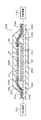
- FIG. 2 is a cross-sectional view taken along line II-II in FIG. It is explanatory drawing which shows the non-mounting surface of the circuit board.
- 4 is a cross-sectional view illustrating a flexible wiring board 23.
- FIG. 4 is an enlarged view showing a main part of a flexible wiring board 23.
- FIG. 6 is a cross-sectional view for explaining an example of a connection process between the connection terminal 26 of the circuit board 22 and the connection terminal 236 of the flexible wiring board 23.
- FIG. 12 is a cross-sectional view for explaining another example of a connection process between the connection terminal 26 of the circuit board 22 and the connection terminal 236 of the flexible wiring board 23.
- FIG. 2 is a cross-sectional view taken along line XII-XII in FIG. It is sectional drawing for demonstrating the manufacturing procedure of the electronic circuit apparatus 20B.
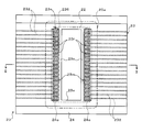
- FIG. 1 is a plan view showing an electronic circuit device according to an embodiment of the present invention
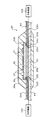
- FIG. 2 is a sectional view taken along line II-II in FIG.
- the electronic circuit device 20 of the embodiment shown in these drawings is configured as an electronic control device that controls a vehicle automatic transmission (not shown), and is mounted, for example, on a unit base fixed to a lower portion of a transmission case.
- the electronic circuit device 20 according to the embodiment includes a circuit board 22 on which various electronic components 21 are mounted, and flexible wiring that is bonded to the circuit board 22 and enables electrical connection between the circuit board 22 and the external device 100.
- the circuit board 22 is made of a base material made of a material having excellent heat resistance and thermal conductivity, such as ceramic, and having a relatively small coefficient of thermal expansion, and a wiring pattern formed on one surface of the base material. Have.
- the surface of the circuit board 22 on which the wiring pattern is formed is used as a mounting surface for a plurality of electronic components 21 including IC chips.
- a plurality of connection terminals (circuit side connection terminals) connected to the wiring pattern on the mounting surface side, respectively. 26 are juxtaposed along each of a pair of side edges of the circuit board 22 facing each other.
- the circuit board 22 has two rows of a plurality of connection terminals 26 on the non-mounting surface.
- a test terminal (not shown) that is used when performing a continuity test or a function test of a circuit on the circuit board 22 may be disposed on the non-mounting surface of the circuit board 22.
- the flexible wiring board 23 is a flexible and deformable wiring material having a thickness of about 0.1 to 0.2 mm, for example.
- the flexible wiring board 23 included in the electronic circuit device 20 of the embodiment has a so-called single-sided structure as shown in FIG. 4, and a base film 230 formed of a resin such as a polyimide resin, and the base film 230 on the base film 230.
- the wiring conductor 232 made of a copper foil or the like attached to the wiring layer 231 with the adhesive layer 231 and the wiring conductor 232 attached to the wiring conductor 232 or the base film 230 via the adhesive layer 233.
- a cover film 234 for covering.
- a connector (not shown) for connection with the external device 100 is connected to the flexible wiring board 23 (wiring conductor 232).
- the external device 100 connected to the circuit board 22 via the flexible wiring board 23 includes various sensors such as a solenoid valve, an oil temperature sensor, and a hydraulic sensor included in a hydraulic circuit that operates a hydraulic clutch and a hydraulic brake of an automatic transmission. Other electronic control units etc. are included.
- an opening 23 o is formed in the flexible wiring board 23 so as to face the non-mounting surface of the circuit board 22.
- the size of the opening 23o is determined to be as large as possible within a range in which the peripheral portion of the non-mounting surface of the circuit board 22 can sufficiently come into contact with the cover film 234 of the flexible wiring board 23.
- the flexible wiring board 23 is connected to a corresponding wiring conductor 232 and a plurality of connection terminals (so as to be opposed to the corresponding connection terminals 26 of the circuit board 22). Wiring board side connection terminal) 236.
- connection terminals 236 are juxtaposed on the front surface side (the cover film 234 side) of the flexible wiring board 23 along each of a pair of opposite edges of the opening 23o. That is, the flexible wiring board 23 has two rows of a plurality of connection terminals 236 on the cover film 234 side, and each connection terminal 236 is exposed from the cover film 234 and connected to the corresponding connection terminal 26 of the circuit board 22. Electrically connected.
- the flexible substrate 23 includes a plurality of free end portions 23f formed so as to include at least one connection terminal 236, and between the free end portions 23f and the openings 23o. And a spacer portion 23s located at the same position.
- each free end 23 f has a narrow first slit 23 m formed in the flexible wiring board 23 so as to extend in the direction in which the plurality of connection terminals 236 are arranged, and a first slit 23 m. It is defined by a plurality of second slits 23n which are continuous and extend between the connection terminals 26 adjacent to each other.
- the first slit 23m extends in parallel to the edge with a predetermined distance from the edge of the opening 23o extending along the plurality of connection terminals 236, and thereby the opening 23o and the first slit 23m.
- a narrow spacer portion 23s is formed (remained) between the two.
- each second slit 23n extends from the first slit 23m to a position beyond the connection terminal 26 to some extent in a direction substantially orthogonal to the first slit 23m.
- a slight gap is defined between the adjacent free end portions 23f.
- the flexible wiring board 23 (cover film 234) having such a configuration is bonded so that the non-mounting surface of the circuit board 22 faces the heat radiating plate 24 through the opening 23o except for the free end portions 23f. .
- the heat radiating plate 24 is, for example, a rectangular plate made of a low-expansion metal such as ordinary steel (SPCC) or a clad material having a relatively small thermal expansion coefficient in the embodiment, but is thermally conductive such as an aluminum plate or a steel material. It may be a plate made of a material excellent in.
- SPCC ordinary steel
- two long openings 24 o are formed in the heat radiating plate 24 so as to face the plurality of connection terminals 236 of the flexible wiring board 23.
- the heat dissipation plate 24 is a base film of the flexible wiring board 23 except for the free end portions 23f from the side opposite to the circuit board 22 so that each opening 24o faces the corresponding row of connection terminals 236.
- the circuit board 22 is bonded to the semiconductor substrate 230 via a silicon-based heat radiation adhesive layer 30 (not shown) and a silicon-based heat radiation adhesive layer 30 formed in the opening 23o. Bonded to the non-mounting surface. That is, in the electronic circuit device 20 of the embodiment, the circuit board 22 is thermally connected to the heat dissipation plate 24 via the adhesive layer 30 made of a heat dissipation adhesive having a relatively large area. Further, the heat dissipation plate 24 of the embodiment has a width longer than the width of the flexible wiring board 23 (the length in the direction in which the connection terminals 26 are arranged in parallel). In the electronic circuit device 20 of the embodiment, FIG. As shown, there are regions where the flexible wiring board 23 is not bonded to both ends of the heat dissipation plate 24 in the width direction.
- the sealing resin portions 25a and 25b are formed by setting a circuit board 22, a flexible wiring board 23 and a heat radiating plate 24 which are bonded and integrated with each other in a mold, and then heat and press a thermosetting resin such as an epoxy resin. It is formed by transfer molding which melts and injects and presses molten resin into the mold. As shown in FIGS. 1 and 2, the upper sealing resin portion 25a in the drawing seals the circuit board 22 and a part of the flexible wiring board 23, and the lower sealing resin portion 25b in the drawing is A part of the heat radiating plate 24 is sealed.
- the shape (mass) and position of the upper sealing resin portion 25a in the figure and the lower sealing resin portion 25b in the figure are reduced by stress acting between the sealing resin portions 25a, 25b and other members. Determined to be.
- the sealing resin portions 25a and 25b are formed so as to sufficiently expose the portion of the heat radiating plate 24 where the flexible wiring board 23 is not bonded.
- an ATF automated transmission fluid
- heat generated in the circuit board 22 is released to the outside by heat exchange between the surfaces of the sealing resin portions 25a and 25b and the ATF.
- the circuit board 22 on which the electronic component 21 is mounted the flexible wiring board 23 having a plurality of connection terminals 236, a plurality of free end portions 23f, and a spacer portion 23s, and an opening 24o are provided.
- the base film 230 of the flexible wiring board 23 and the heat radiating plate 24 are bonded to each other with a heat radiating adhesive while each opening 24o faces a corresponding plurality of connection terminals 236. .
- each free end portion 23f (base film 230) of the flexible wiring board 23 and the heat radiating plate 24 are not bonded by the heat radiating adhesive, but each spacer portion 23s (base film 230) of the flexible wiring board 23 and the heat radiating plate 24 are bonded. Are bonded to each other via a heat dissipating adhesive.
- each connection terminal 26 of the circuit board 22 corresponds to the corresponding connection terminal on the surface of the flexible wiring board 23, that is, the surface opposite to the bonding surface with the heat radiating plate 24.
- the non-mounting surface of the circuit board 22 and the cover film 234 of the flexible wiring board 23 are bonded to each other by a heat-dissipating adhesive, and the non-mounting surface of the circuit board 22 and the heat-dissipating plate 24 are connected to the flexible wiring board. It adhere
- connection terminals 26 of the circuit board 22 and the connection terminals 236 of the flexible wiring board 23 facing each other as shown in FIG.
- a bonding material 27 such as a conductive paste is disposed.
- the circuit board 22 and the flexible wiring board 23 are bonded, the circuit board 22 and the free end portions 23f (cover film 234) of the flexible wiring board 23 are not bonded by the heat radiation adhesive, but the circuit board 22 and the flexible wiring board are not bonded.
- the spacers 23s (cover film 234) of the plate 23 are bonded to each other through a heat radiation adhesive.
- the spacer part 23s adhered to the circuit board 22 and the heat radiating plate 24 is provided (remaining) between the opening 23o and the free end part 23f of the flexible wiring board 23, the spacer part 23s can be removed.
- the thickness makes it possible to more appropriately manage the thickness of the adhesive layer 30, and to ensure the heat dissipation of the circuit board 22, while further improving the insulation of the non-mounting surface (for example, a test terminal not shown) of the circuit board 22. It can be ensured satisfactorily.
- the pulse heater H is inserted into the opening 24o of the heat radiating plate 24 and the tip of the pulse heater H is connected to the flexible wiring as shown in FIG.
- the bonding material 27 is pressed against the base film 230 of the plate 23 and heated and melted by pulse heat to electrically connect the connection terminal 26 and the connection terminal 236 facing each other.
- the opening 24o is formed in the heat dissipation plate 24 so as to face the connection terminal 236 of the flexible wiring board 23, the connection terminal 26 of the circuit board 22 and the corresponding connection terminal 236 of the flexible wiring board 23 Can be easily connected.
- the bonding material 27 can be satisfactorily heated and melted only by the heating by the pulse heater H through the opening 24o of the heat radiating plate 24, as shown in FIG. Since the electronic component 21 can be mounted on the back side, the mounting area of the circuit board 22 can be increased thereby.
- a heat conduction pad (not shown) that is thermally connected to the connection terminal 236 via the wiring conductor 232 is provided so as to be exposed from the base film 230, and the pulse heater H is pressed against the heat conduction pad. You may make it hit.
- heat conduction pads 28 are arranged on the mounting surface of the circuit board 22 so as to face the connection terminals 26, and the heat conduction pads 28 and the corresponding connection terminals 26 are heated.
- connection terminal 26 of the circuit board 22 and the connection terminal 236 of the flexible wiring board 23 are electrically connected, as shown in FIG. Since it is possible to apply heat to the bonding material 27 not only from the 24 side but also from the circuit board 22 side, the electrical connection between the connection terminal 26 and the connection terminal 236 can be realized quickly, and both An electrical connection can be made reliably.
- the circuit board 22, the flexible wiring board 23, and the heat dissipation plate 24 that are bonded and integrated are integrated. It sets in a metal mold
- the resin since the resin also flows into the opening 24 o of the heat radiating plate 24, in the completed electronic circuit device 20, compared with the case where the opening 24 o does not exist in the heat radiating plate 24.
- the heat radiation performance of the heat radiating plate 24 is slightly lowered.
- the length in the width direction of the heat dissipation plate 24 (the direction in which the connection terminals 26 are arranged in parallel) is longer than the width of the flexible wiring board 23, and then the width direction of the heat dissipation plate 24.
- the sealing resin portions 25a and 25b are molded so as to secure a region where the flexible wiring board 23 is not bonded to both ends of the heat dissipation plate 24 and to sufficiently expose the portion of the heat radiating plate 24 where the flexible wiring board 23 is not bonded. Thereby, it becomes possible to ensure favorable heat dissipation performance of the heat dissipation plate 24.
- the flexible wiring board 23 included in the electronic circuit device 20 has the surface (the heat dissipation plate 24 and the heat dissipation plate 24) so as to face the plurality of connection terminals 26 arranged in parallel on the non-mounting surface of the circuit board 22.
- the free end portion 23f of the flexible wiring board 23 is not bonded to the circuit board 22 and the heat radiating plate 24, and the connection terminal 26 of the circuit board 22 and the corresponding connection terminal 236 are electrically opposed to each other. Connected.
- the free end portions 23f of the flexible wiring board 23 can move to some extent with respect to the circuit board 22 and the heat dissipation plate 24. Even if the circuit board 22, the heat radiating plate 24, or the like is subjected to vibration or a thermal shock is applied during or after the manufacture of the device 20, the flexible wiring board 23 is formed around the connection portion with the connection terminal 236 of the circuit board 22. The acting stress can be relaxed. Therefore, it is possible to improve the periphery of the connection portion between the connection terminal 26 and the connection terminal 236 and thus the reliability of the electronic circuit device 20.
- the free end part 23f in the said Example is each formed so that the one connection terminal 236 may be included, it is not restricted to this. That is, the free end portion 23f of the flexible wiring board 23 may be formed to include a plurality of connection terminals 236 as long as a stress relaxation effect can be obtained.
- the first slit 23m extending in the direction in which the connection terminals 236 are arranged in parallel to the flexible wiring board 23, and the first slit 23m between the adjacent connection terminals 236 are arranged in parallel. If the second slit 23n extending to at least the position exceeding the connection terminal 236 is formed in a direction substantially orthogonal to the direction, the plurality of free end portions 23f can be easily configured. Note that the first slit 23m and the second slit 23n are formed at a simple notch and an end of the notch as illustrated in FIG. 8 instead of having a slight width as illustrated in FIG. You may employ
- the heat radiation plate 24 is bonded to the portion other than the free end portion 23f of the flexible wiring board 23 from the side opposite to the circuit board 22, so that the heat dissipation of the circuit board 22 is achieved. Can be secured. Moreover, since the opening 24o is formed in the heat dissipation plate 24 so as to face the plurality of connection terminals 236 of the flexible wiring board 23, the connection terminals 26 and the flexible wiring arranged in parallel on the non-mounting surface of the circuit board 22 are formed.
- the pulse heater H is inserted into the opening 24o of the heat radiating plate 24 in a state where the connection terminal 236 arranged in parallel to the surface opposite to the surface of the plate 23 opposite to the bonding surface to the heat radiating plate 24 is opposed to the connection terminal 26.
- the connection terminal 26 of the circuit board 22 and the corresponding connection terminal 236 of the flexible wiring board 23 can be easily connected.
- the flexible wiring board 23 is not bonded to both ends of the heat dissipation plate 24 in the direction in which the connection terminals 236 are arranged, and the both ends are not covered with the sealing resin portions 25a and 25b. Thereby, even if the opening 24o having a certain opening area is formed in the heat radiating plate 24, the heat radiating performance of the heat radiating plate 24 can be ensured satisfactorily.
- an opening 23o is formed in the flexible wiring board 23 so as to face the non-mounting surface of the circuit board 22, and an adhesive layer 30 is formed in which the non-mounting surface of the circuit board 22 and the heat dissipation plate 24 are formed in the opening 23o. If they are bonded to each other, the heat dissipation of the circuit board 22 of the electronic circuit device 20 is ensured satisfactorily by a simple structure, and the non-mounting surface (test terminal) of the circuit board 22 and the heat dissipation plate 24 are well insulated. It becomes possible to do.
- a flexible wiring board 23A having a so-called double-sided structure as shown in FIG. 9 may be employed.
- a flexible wiring board 23A shown in FIG. 9 has a base film 230 formed of a resin such as a polyimide resin, and a wiring for a copper foil or the like attached to one surface of the base film 230 via an adhesive layer 231u.
- a cover film (second cover film) 234l covering the conductor 232l.
- the wiring conductor 232u connected to the connection terminal 236 and the heat radiating plate 24 side with respect to the flexible wiring board 23A.
- a thermal conduction via 239 for thermally connecting the wiring conductor 232l (or a copper foil not used as wiring) is disposed in the same layer as the base film 230, and is thermally connected to the wiring conductor 232l on the heat radiation plate 24 side. It is preferable to provide a heat conduction pad (heat transfer material) 238 connected to the radiating plate 24 so as to be exposed from the cover film 234l on the heat radiating plate 24 side.
- the double-sided structure is thicker than the flexible wiring board 23 having the single-sided structure. Even when the flexible wiring board 23 ⁇ / b> A having the above is used, it is possible to easily and efficiently execute the connection process between the connection terminal 26 and the connection terminal 236 by transferring heat to the bonding material 27 satisfactorily. .
- FIG. 11 is a plan view showing an electronic circuit device 20B according to a modification
- FIG. 12 is a cross-sectional view taken along line XII-XII in FIG.
- a plurality of connection terminals 26 are arranged in parallel on the mounting surface of the circuit board 22B, and the flexible wiring board 23B having a single-sided structure, that is, the circuit board 22B is connected to the circuit board 22B.
- a plurality of connection terminals 236 are arranged in parallel on the surface opposite to the bonding surface. Further, as shown in FIG.
- the slits extending between the connection terminals 26 adjacent to each other are compared to the flexible wiring board 23 illustrated in FIG.
- the length of each free end 23f is longer than that of the flexible wiring board 23 illustrated in FIG.
- no opening is formed in the heat dissipation plate 24B of the electronic circuit device 20B.
- the connection terminals 26 of the circuit board 22B and the corresponding connection terminals 236 of the flexible wiring board 23B are electrically connected with the plurality of free end portions 23f riding on the circuit board 22B. It is connected.
- the electronic circuit apparatus 20B when vibration is applied to the circuit board 22B or the heat radiating plate 24B or a thermal shock is applied, the electronic circuit apparatus 20B is flexible around the connection portion with the connection terminal 236 of the circuit board 22B.
- the stress acting on the wiring board 23B can be relaxed.
- a circuit board 22B on which the electronic component 21 is mounted a flexible wiring board 23B having a plurality of connection terminals 236, a plurality of free end portions 23f, and a spacer portion 23s
- the base film 230 of the flexible wiring board 23B and the heat radiating plate 24B are bonded to each other with a heat radiating adhesive.
- each free end portion 23f (base film 230) of the flexible wiring board 23B and the heat radiating plate 24B are not bonded by the heat radiating adhesive, but each spacer portion 23s (base film 230) of the flexible wiring board 23B and the heat radiating plate 24B.
- a heat dissipating adhesive are bonded to each other via a heat dissipating adhesive.
- each free end portion 23f of the flexible wiring board 23B rides on the circuit board 22B, and each connection terminal 26 of the circuit board 22B faces the corresponding connection terminal 236 of the flexible wiring board 23B.
- the non-mounting surface and the cover film 234 of the flexible wiring board 23 are adhered by a heat radiation adhesive, and the non-mounting surface of the circuit board 22B and the heat radiation plate 24B are disposed by the heat radiation adhesive disposed in the opening 23o of the flexible wiring board 23B.
- Glue Glue.
- a bonding material such as ACF (Anisotropic Condactive Film) is disposed between the connection terminal 26 of the circuit board 22B and the connection terminal 236 of the flexible wiring board 23B facing each other.
- the circuit board 22B and the flexible wiring board 23B are bonded, the circuit board 22B and the free end portions 23f of the flexible wiring board 23B are not bonded by the heat-dissipating adhesive, but the spacers of the circuit board 22B and the flexible wiring board 23B.
- the part 23s (cover film 234) is bonded to each other via a heat radiation adhesive.
- the tip of the pulse heater is pressed against the cover film 234 of the flexible wiring board 23B from above the connection terminal 236, and the bonding material is heated by pulse heat.
- the connection terminal 26 and the connection terminal 236 which are melted and face each other are electrically connected.
- a heat conduction pad (not shown) that is thermally connected to the connection terminal 236 via the wiring conductor 232 is provided so as to be exposed from the cover film 234, and a pulse heater is pressed against the heat conduction pad. You may do it.
- the circuit board 22B, the flexible wiring board 23B and the heat radiating plate 24B which are bonded and integrated with each other are set in a mold, and the sealing resin portions 25a and 25b are formed by transfer molding.
- a flexible wiring board 23C having a so-called double-sided structure as illustrated in FIG. 9 is employed instead of the flexible wiring board 23B having a single-sided structure. May be.
- a thermal conduction via 239 that thermally connects a copper foil that is not used as a wiring) is disposed in the same layer as the base film 230 and is thermally connected to the upper wiring conductor 232u in the drawing.
- a pad (heat transfer material) 238 may be provided so as to be exposed from the upper cover film 234u in the drawing. Thereby, if the tip of the pulse heater H is pressed against the heat conduction pad 238, even when the flexible wiring board 23C having a thick double-sided structure is used compared to the flexible wiring board 23 having a single-sided structure, It is possible to easily and efficiently execute the connection process between the connection terminal 26 and the connection terminal 236 by transferring heat to the bonding material.
- heat conduction pads 28 are arranged on the non-mounting surface of the circuit board 22 so as to face the connection terminals 26, and the heat conduction pads 28 and the corresponding connection terminals 26 are arranged.
- the thermal connection via 29 may be thermally connected.
- the non-mounting surface of the circuit board 22 and the flexible wiring board 23 are bonded, but the circuit board 22 and the flexible wiring board 23 are not bonded to each other, and the circuit
- the substrate 22 may be bonded only to the heat dissipation plate 24 and the flexible wiring board 23 may be bonded only to the heat dissipation plate 24.
- the electronic circuit devices 20 and 20B include sealing resin portions 25a and 25b made of resin molded so as to seal the circuit board 22, a part of the flexible wiring board 23, and a part of the heat dissipation plate 24.
- the electronic circuit device 20 or the like may be configured to have a cover that covers a part of the circuit board 22 or the flexible wiring board 23 instead of the sealing resin portion. Absent. Furthermore, although the above-described electronic circuit device 20 and the like have been described as being used for controlling a vehicle automatic transmission, the present invention is not limited to this. That is, the electronic circuit device 20 or the like may be configured as an electronic control unit that controls other in-vehicle devices such as an internal combustion engine or an electric motor, or may be configured as an electronic circuit device that controls devices other than the in-vehicle devices. .
- circuit boards 22 and 22B on which the electronic components 21 are mounted correspond to “circuit boards”, and the flexible wiring board that enables the circuit board 22 and the external device 100 to be electrically connected.
- 23, 23A, 23B, and 23C correspond to “flexible wiring boards”, and the connection terminals 26 arranged in parallel on the mounting surface or non-mounting surface of the circuit board 22 correspond to “circuit side connection terminals”.
- connection terminals 236 arranged side by side on either the front or back surface of the flexible wiring board 23 or the like so as to face the plurality of connection terminals 26 correspond to “wiring board side connection terminals”, and at least one connection terminal 236 is provided.
- the free end portion 23f formed to include the “free end portion” corresponds to the “radiation end portion”, and the heat radiation plates 24 and 24B bonded to the flexible wiring board 23 and the like correspond to “the heat radiation member”.
- a sealing resin portion 25a made of molded resin so as to seal a portion of such part and the heat radiating plate 24 such as a flexible wiring board 23, 25b corresponds to the "sealing resin portion”.
- the present invention can be used in the electronic circuit device manufacturing industry.
Landscapes
- Engineering & Computer Science (AREA)
- Microelectronics & Electronic Packaging (AREA)
- Manufacturing & Machinery (AREA)
- Combinations Of Printed Boards (AREA)
- Structure Of Printed Boards (AREA)
Abstract
電子回路装置20は、電子部品21が実装された回路基板22と、この回路基板22と外部機器との電気的接続を可能とするフレキシブル配線板23とを含み、回路基板22は、非実装面に並設された複数の接続端子26を有し、フレキシブル配線板23は、回路基板22の接続端子26と対向するように表面に並設された複数の接続端子236と、それぞれ1つの接続端子236を含むように形成された複数の遊端部23fとを有し、各遊端部23fは回路基板22に接着されず、接続端子26とそれに対応した接続端子26とが互いに対向し合う状態で電気的に接続される。
Description
本発明は、電子回路装置に関し、特に、電子部品が実装された回路基板を含む電子回路装置に関する。
従来から、この種の電子回路装置として、電子部品が搭載されると共に表面に形成された複数のランドにバンプまたは導電性ボールが接合された回路基板と、可撓性および電気絶縁性を有する樹脂フィルム内に配線用導体が回路基板から接離する方向に延びるようにパターニングされると共に配線用導体のランドが回路基板のバンプまたは導電性ボールと接合されたフレキシブル配線板と、電子部品、回路基板、バンプまたは導電性ボールを介したフレキシブル配線板と回路基板との電気接続部を封止するモールド樹脂とを備えたものが提案されている(例えば、特許文献1参照)。
上記特許文献1に記載された技術のように、バンプ等を介して回路基板側のランドとフレキシブル配線板側のランドとを接続すれば、高コスト化の要因となるワイヤボンディング工程を無くしてコストダウンを図ると共に回路基板とフレキシブル配線板との電気的接続に要するスペースを削減することができる。しかしながら、特許文献1に記載された技術のように回路基板側のランドとフレキシブル配線板側のランドとを接続した場合、回路基板等に振動が作用したときにフレキシブル配線板のランド周辺の応力が高まってフレキシブル配線板が破損したり、端子の接続信頼性を損なったりするおそれもある。また、回路基板等に熱衝撃が加えられると、回路基板とフレキシブル配線板との熱膨張係数の相違に起因してフレキシブル配線板のランド周辺の応力が高まってフレキシブル配線板が破損したり、端子の接続信頼性を損なったりするおそれもある。
そこで、本発明は、回路基板側の接続端子との接続部周辺でフレキシブル配線板に作用する応力を緩和することにより電子回路装置の信頼性を向上させることを主目的とする。
本発明の電子回路装置は、上述の主目的を達成するために以下の手段を採っている。
本発明による電子回路装置は、
電子部品が実装された回路基板と、該回路基板と外部機器との電気的接続を可能とするフレキシブル配線板とを含む電子回路装置であって、
前記回路基板は、前記電子部品が実装される実装面または該実装面とは反対側の面である非実装面に並設された複数の回路側接続端子を有し、
前記フレキシブル配線板は、前記回路基板の前記複数の回路側接続端子と対向するように表面および裏面の何れか一方に並設された複数の配線板側接続端子と、それぞれ少なくとも1つの前記配線板側接続端子を含むように形成された複数の遊端部とを有し、
前記フレキシブル配線板の前記遊端部は前記回路基板に接着されず、前記回路側接続端子とそれに対応した前記配線板側接続端子とが互いに対向し合う状態で電気的に接続されることを特徴とする。
電子部品が実装された回路基板と、該回路基板と外部機器との電気的接続を可能とするフレキシブル配線板とを含む電子回路装置であって、
前記回路基板は、前記電子部品が実装される実装面または該実装面とは反対側の面である非実装面に並設された複数の回路側接続端子を有し、
前記フレキシブル配線板は、前記回路基板の前記複数の回路側接続端子と対向するように表面および裏面の何れか一方に並設された複数の配線板側接続端子と、それぞれ少なくとも1つの前記配線板側接続端子を含むように形成された複数の遊端部とを有し、
前記フレキシブル配線板の前記遊端部は前記回路基板に接着されず、前記回路側接続端子とそれに対応した前記配線板側接続端子とが互いに対向し合う状態で電気的に接続されることを特徴とする。
この電子回路装置のフレキシブル配線板は、回路基板の実装面または非実装面に並設された複数の回路側接続端子と対向するように表裏面の何れか一方に並設された複数の配線板側接続端子と、それぞれ少なくとも1つの配線板側接続端子を含むように形成された複数の遊端部とを有する。そして、フレキシブル配線板の遊端部は回路基板に接着されず、回路基板の回路側接続端子とそれに対応した配線板側接続端子とが互いに対向し合う状態で電気的に接続される。これにより、フレキシブル配線板の各遊端部は、回路基板に対してある程度移動可能となることから、回路基板等に振動が作用したり熱衝撃が加えられたりしても、回路側接続端子との接続部周辺でフレキシブル配線板に作用する応力を緩和することができる。この結果、回路側接続端子と配線板側接続端子との接続部周辺ひいては電子回路装置の信頼性を向上させることが可能となる。
また、前記フレキシブル配線板の前記遊端部は、前記配線板側接続端子の並設方向に延びるように前記フレキシブル配線板に形成された第1のスリットと、互いに隣り合う前記配線板側接続端子同士の間で前記第1のスリットから前記並設方向と概ね直交する方向に少なくとも前記配線板側接続端子を超える位置まで延びるように前記フレキシブル配線板に形成された複数の第2のスリットとにより画成されてもよい。これにより、遊端部を容易に構成することができる。なお、第1および第2のスリットは、多少の幅をもったものであってよく、また単純な切り込みであってもよい。
そして、前記電子回路装置は、前記フレキシブル配線板の前記遊端部以外の部位に対して前記回路基板とは反対側から接着された放熱部材を更に備えてもよく、前記複数の回路側接続端子は、前記回路基板の前記非実装面に並設されてもよく、前記複数の配線板側接続端子は、前記フレキシブル配線板の前記放熱部材との接着面とは反対側の面に並設されてもよく、前記放熱部材には、前記フレキシブル配線板の前記複数の配線板側接続端子と対向するように開口が形成されてもよい。このように、放熱部材を用いることにより、回路基板の放熱性を確保することが可能となる。また、放熱部材にフレキシブル配線板の配線板側接続端子と対向するように開口を形成しておけば、回路基板の非実装面に並設された回路側接続端子とフレキシブル配線板の放熱部材との接着面とは反対側の面に並設された配線板側接続端子とを対向させた状態で放熱部材の開口にヒータを挿入して回路側接続端子と配線板側接続端子とを加熱することにより、回路基板の回路側接続端子とそれに対応するフレキシブル配線板の配線板側接続端子とを容易に接続することができる。
更に、前記放熱部材の前記並設方向における両端部の少なくとも一部には、前記フレキシブル配線板が接着されないとよい。すなわち、放熱部材に開口を形成すると、その分だけ放熱部材の放熱性能が低下することになる。従って、例えば配線板側接続端子の並設方向における放熱部材の幅を拡大し、放熱部材の当該並設方向における両端部の少なくとも一部にフレキシブル配線板が接着されないようにすれば、放熱部材の放熱性能を良好に確保することが可能となる。
また、前記複数の回路側接続端子は、前記回路基板の前記実装面に並設されてもよく、前記複数の配線板側接続端子は、前記フレキシブル配線板の前記回路基板側とは反対側の面に並設されてもよく、前記回路側接続端子とそれに対応した前記配線板側接続端子とは、前記フレキシブル配線板の前記複数の遊端部がそれぞれ前記回路基板上に乗り上げる状態で電気的に接続されてもよい。このような構造を採用しても、回路基板等に振動が作用したり熱衝撃が加えられたりしたときに、回路側接続端子との接続部周辺でフレキシブル配線板に作用する応力を緩和することができる。また、フレキシブル配線板の遊端部に撓みをもたせることで、応力緩和をより効果的に図ることが可能となる。
更に、前記フレキシブル配線板は、前記配線板側接続端子に接続される配線用導体と、該配線用導体に対して前記配線板側接続端子とは反対側から熱的に接続される伝熱材と、前記配線板側接続端子を外部に露出させた状態で前記配線用導体の一方の面を覆う第1のカバーフィルムと、前記伝熱材を外部に露出させた状態で前記配線用導体の他方の面を覆う第2のカバーフィルムとを含むものであってもよい。これにより、第2のカバーフィルムから露出する伝熱材に熱を付与すれば、回路側接続端子と配線板側接続端子とを加熱することができるので、回路側接続端子と配線板側接続端子との接続処理を容易かつ効率よく実行することが可能となる。
また、前記フレキシブル配線板には、前記回路基板の前記非実装面と対向するように開口が形成されてもよく、前記回路基板の前記非実装面と前記放熱部材とは、前記開口内に形成される放熱接着剤の層を介して互いに接着されてもよく、前記フレキシブル配線板は、前記開口と前記遊端部との間に前記回路基板と前記放熱部材とに接着されるスペーサ部を含むものであってもよい。これにより、シンプルな構造により電子回路装置の回路基板の放熱性を良好に確保すると共に、回路基板の非実装面と放熱部材とを良好に絶縁することが可能となる。更に、開口と遊端部との間にスペーサ部を設ける(残す)ことにより、当該スペーサ部の厚みにより放熱接着剤の層の厚みを管理することが可能となる。
そして、前記電子回路装置は、前記回路基板と前記フレキシブル配線板の一部を封止するようにモールド成形された樹脂からなる封止樹脂部を更に備えてもよい。
次に、本発明を実施するための形態を実施例を用いて説明する。
図1は、本発明の一実施例に係る電子回路装置を示す平面図であり、図2は、図1のII-II線に沿った断面図である。これらの図面に示す実施例の電子回路装置20は、図示しない車両用自動変速機を制御する電子制御装置として構成されており、例えばトランスミッションケースの下部に固定されたユニット台に搭載される。そして、実施例の電子回路装置20は、各種電子部品21が実装される回路基板22と、回路基板22に接着されて当該回路基板22と外部機器100との電気的接続を可能とするフレキシブル配線板(FPC:Flexible Printed Circuit Board)23と、フレキシブル配線板23に接着された放熱プレート(ヒートシンク)24と、回路基板22とフレキシブル配線板23の一部と放熱プレート24の一部とを封止するように成形された樹脂からなる封止樹脂部25aおよび25bとを備える。
回路基板22は、セラミックといった耐熱性と熱伝導性とに優れると共に比較的小さい熱膨張係数をもった材料により形成された基材からなり、この基材の一方の面に形成された配線パターンを有する。回路基板22の配線パターンが形成された面は、ICチップを始めとする複数の電子部品21の実装面とされる。また、回路基板22の実装面とは反対側の面である非実装面には、図3に示すように、それぞれ実装面側の配線パターンに接続された複数の接続端子(回路側接続端子)26が回路基板22の互いに対向し合う一対の側縁部のそれぞれに沿って並設されている。すなわち、回路基板22は、複数の接続端子26からなる列を非実装面に2列有している。なお、回路基板22の非実装面には、回路基板22上の回路の導通検査や機能検査等の実行に際して用いられる図示しないテスト用端子が配置されてもよい。
フレキシブル配線板23は、可撓性をもった変形可能な配線材であって、例えば0.1~0.2mm程度の厚みを有するものである。実施例の電子回路装置20に含まれるフレキシブル配線板23は、図4に示すような、いわゆる片面構造を有するものであり、ポリイミド樹脂といった樹脂により形成されたベースフィルム230と、このベースフィルム230上に接着剤層231を介して貼着された銅箔等からなる配線用導体232と、配線用導体232やベースフィルム230に対して接着剤層233を介して貼着されて配線用導体232を覆うカバーフィルム234とを含む。フレキシブル配線板23(配線用導体232)には、外部機器100との接続に供されるコネクタ(図示省略)が接続されている。フレキシブル配線板23を介して回路基板22と接続される外部機器100には、自動変速機の油圧クラッチや油圧ブレーキを作動させる油圧回路に含まれるソレノイドバルブ、油温センサや油圧センサといった各種センサ類、他の電子制御ユニット等が含まれる。
図1に示すように、フレキシブル配線板23には、回路基板22の非実装面と対向するように開口23oが形成されている。実施例において、開口23oのサイズは、回路基板22の非実装面の周縁部がフレキシブル配線板23のカバーフィルム234と充分に当接可能となる範囲内でできるだけ大きくなるように定められる。また、フレキシブル配線板23は、図1に示すように、それぞれ対応する配線用導体232に接続されると共に回路基板22の対応する接続端子26と対向するように配設された複数の接続端子(配線板側接続端子)236を有する。実施例において、接続端子236は、開口23oの互いに対向し合う一対の縁部のそれぞれに沿ってフレキシブル配線板23の表面側(カバーフィルム234側)に並設されている。すなわち、フレキシブル配線板23は、複数の接続端子236からなる列をカバーフィルム234側に2列有し、各接続端子236は、カバーフィルム234から露出されて回路基板22の対応する接続端子26と電気的に接続される。
更に、フレキシブル基板23は、図1および図2に示すように、それぞれ少なくとも1つの接続端子236を含むように形成された複数の遊端部23fと、各遊端部23fと開口23oとの間に位置するスペーサ部23sとを有する。各遊端部23fは、図5に示すように、複数の接続端子236の並設方向に延びるようにフレキシブル配線板23に形成された細幅の第1スリット23mと、それぞれ第1スリット23mに連なると共に互いに隣り合う接続端子26同士の間に延在する複数の第2スリット23nとにより画成される。すなわち、第1スリット23mは、複数の接続端子236に沿って延びる開口23oの縁部から外側に所定間隔をおいて当該縁部と平行に延在し、これにより、開口23oと第1スリット23mとの間に細幅のスペーサ部23sが形成される(残される)ことになる。また、実施例において、各第2スリット23nは、図5に示すように、第1スリット23mから外方かつ当該第1スリット23mと概ね直交する方向に接続端子26をある程度超える位置まで延出され、互いに隣り合う遊端部23f同士の間に僅かな隙間を画成する。このような構成を有するフレキシブル配線板23(カバーフィルム234)には、各遊端部23fを除いて回路基板22の非実装面が開口23oを介して放熱プレート24と対向するように接着される。
放熱プレート24は、実施例において比較的小さい熱膨張係数をもった普通鋼(SPCC)やクラッド材といった低膨張性金属からなる例えば矩形状の板体であるが、アルミ板や鋼材といった熱伝導性に優れる材料からなる板体であってもよい。図1および図2に示すように、放熱プレート24には、フレキシブル配線板23の複数の接続端子236と対向するように2つの長尺の開口24oが形成されている。図2に示すように、放熱プレート24は、各開口24oが対応する接続端子236の列と対向するように回路基板22とは反対側から各遊端部23fを除くフレキシブル配線板23のベースフィルム230に対してシリコン系の放熱接着剤の層(図示せず)を介して接着されると共に、開口23o内に形成されるシリコン系の放熱接着剤からなる接着剤層30を介して回路基板22の非実装面に接着される。すなわち、実施例の電子回路装置20では、回路基板22は、比較的広い面積をもった放熱接着剤からなる接着剤層30を介して放熱プレート24と熱的に接続されることになる。また、実施例の放熱プレート24は、フレキシブル配線板23の幅(接続端子26の並設方向における長さ)よりも長い幅を有しており、実施例の電子回路装置20では、図1に示すように、放熱プレート24の幅方向における両端部にフレキシブル配線板23が接着されない領域が存在する。
封止樹脂部25aおよび25bは、互いに接着されて一体化した回路基板22、フレキシブル配線板23および放熱プレート24を金型内にセットした後、例えばエポキシ樹脂といった熱硬化性樹脂を加熱加圧して溶融させると共に、溶融樹脂を金型内に注入・加圧するトランスファーモールド成形により成形される。図1および図2に示すように、図中上側の封止樹脂部25aは、回路基板22とフレキシブル配線板23の一部とを封止し、図中下側の封止樹脂部25bは、放熱プレート24の一部を封止する。図中上側の封止樹脂部25aと図中下側の封止樹脂部25bとの形状(質量)や位置は、封止樹脂部25a,25bと他の部材との間に作用する応力が緩和されるように定められる。また、実施例において、封止樹脂部25aおよび25bは、放熱プレート24のフレキシブル配線板23が接着されない部分を充分に露出させるように形成される。なお、実施例の電子回路装置20が配置される自動変速機のユニット台にはATF(オートマチックトランスミッションフルード)が導入され、放熱プレート24の封止樹脂部25aおよび25bにより封止されていない露出部や封止樹脂部25aおよび25bの表面とATFとが熱交換することにより回路基板22にて発生する熱が外部に放出されることになる。
次に、実施例に係る電子回路装置20の製造手順の一例を説明する。電子回路装置20を製造するに際しては、電子部品21が実装された回路基板22と、複数の接続端子236や複数の遊端部23f、スペーサ部23sを有するフレキシブル配線板23と、開口24oを有する放熱プレート24とを用意した上で、まず、各開口24oが対応する複数の接続端子236と対向するようにしながらフレキシブル配線板23のベースフィルム230と放熱プレート24とを放熱接着剤により互いに接着する。この際、フレキシブル配線板23の各遊端部23f(ベースフィルム230)と放熱プレート24とは放熱接着剤により接着されないが、フレキシブル配線板23の各スペーサ部23s(ベースフィルム230)と放熱プレート24とは放熱接着剤を介して互いに接着される。
フレキシブル配線板23と放熱プレート24とを互いに接着したならば、回路基板22の各接続端子26がフレキシブル配線板23の表面すなわち放熱プレート24との接着面とは反対側の面の対応する接続端子236と対向するようにしながら、回路基板22の非実装面とフレキシブル配線板23のカバーフィルム234とを放熱接着剤により接着すると共に、回路基板22の非実装面と放熱プレート24とをフレキシブル配線板23の開口23o内に配置した放熱接着剤により接着する。この際、互いに対向し合う回路基板22の接続端子26とフレキシブル配線板23の接続端子236との間には、図6に示すように、ACF(Anisotropic Condactive Film)等の導電性接着剤やハンダあるい導電性ペーストといったボンディング材27を配置する。また、回路基板22とフレキシブル配線板23との接着に際して、回路基板22とフレキシブル配線板23の各遊端部23f(カバーフィルム234)とは放熱接着剤により接着されないが、回路基板22とフレキシブル配線板23の各スペーサ部23s(カバーフィルム234)とは放熱接着剤を介して互いに接着される。このように、フレキシブル配線板23の開口23oと遊端部23fとの間に回路基板22と放熱プレート24とに接着されるスペーサ部23sを設けて(残して)おけば、当該スペーサ部23sの厚みにより接着剤層30の厚みをより適正に管理することが可能となり、回路基板22の放熱性を確保しつつ、回路基板22の非実装面(例えば図示しないテスト用端子)の絶縁性をより良好に確保することができる。
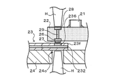
回路基板22をフレキシブル配線板23や放熱プレート24に対して接着したならば、図6に示すように、放熱プレート24の開口24o内にパルスヒータHを挿入すると共にパルスヒータHの先端をフレキシブル配線板23のベースフィルム230に押し当て、パルスヒートによりボンディング材27を加熱溶融させて互いに対向し合う接続端子26と接続端子236とを電気的に接続する。このように、放熱プレート24にフレキシブル配線板23の接続端子236と対向するように開口24oを形成しておけば、回路基板22の接続端子26とそれに対応するフレキシブル配線板23の接続端子236とを容易に接続することができる。
ここで、放熱プレート24の開口24oを介したパルスヒータHによる加熱のみでボンディング材27を良好に加熱溶融させることができる場合には、図6に示すように、回路基板22の接続端子26の裏側にも電子部品21を実装可能となるので、それにより回路基板22の実装面積を拡大することができる。この場合、配線用導体232を介して接続端子236と熱的に接続される図示しない熱伝導用パッドをベースフィルム230から露出するように設けておき、当該熱伝導用パッドにパルスヒータHを押し当てるようにしてもよい。また、図7に示すように、回路基板22の実装面に各接続端子26と対向するように熱伝導用パッド28を配置すると共に、熱伝導用パッド28とそれに対応する接続端子26とを熱伝導用ビア29を介して熱的に接続しておいてもよい。これにより、回路基板22の接続端子26とフレキシブル配線板23の接続端子236との電気的接続に際して、図7に示すように、パルスヒータHを熱伝導用パッド28に押し当てることにより、放熱プレート24側のみならず回路基板22側からもボンディング材27に対して熱を付与することが可能となるので、接続端子26と接続端子236との電気的接続を速やかに実現すると共に、両者をより確実に電気的に接続することができる。
こうして、回路基板22の接続端子26とフレキシブル配線板23の接続端子236との電気的な接続が完了したならば、互いに接着されて一体化した回路基板22、フレキシブル配線板23および放熱プレート24を金型内にセットし、トランスファーモールド成形により封止樹脂部25aおよび25bを成形する。この際、図2に示すように、放熱プレート24の開口24o内にも樹脂が流入することになるため、完成後の電子回路装置20では、放熱プレート24に開口24oが存在しない場合に比べて放熱プレート24の放熱性能が若干低下することになる。このため、実施例では、上述のように、放熱プレート24の幅方向(接続端子26の並設方向)における長さをフレキシブル配線板23の幅よりも長くした上で、放熱プレート24の幅方向における両端部にフレキシブル配線板23が接着されない領域を確保すると共に、放熱プレート24のフレキシブル配線板23が接着されない部分を充分に露出させるように封止樹脂部25aおよび25bを成型している。これにより、放熱プレート24の放熱性能を良好に確保することが可能となる。
以上説明したように、実施例の電子回路装置20に含まれるフレキシブル配線板23は、回路基板22の非実装面に並設された複数の接続端子26と対向するように表面(放熱プレート24との接着面とは反対側の面)に並設された複数の接続端子236と、それぞれ1つの接続端子236を含むように形成された複数の遊端部23fとを有する。そして、フレキシブル配線板23の遊端部23fは回路基板22と放熱プレート24とに接着されず、回路基板22の接続端子26とそれに対応した接続端子236とが互いに対向し合う状態で電気的に接続される。これにより、少なくとも封止樹脂部25a,25bが成型される前に、フレキシブル配線板23の各遊端部23fは、回路基板22や放熱プレート24に対してある程度移動可能となることから、電子回路装置20の製造中あるいは完成後に回路基板22や放熱プレート24等に振動が作用したり熱衝撃が加えられたりしても、回路基板22の接続端子236との接続部周辺でフレキシブル配線板23に作用する応力を緩和することができる。従って、接続端子26と接続端子236との接続部周辺ひいては電子回路装置20の信頼性を向上させることが可能となる。なお、上記実施例における遊端部23fは、それぞれ1つの接続端子236を含むように形成されているが、これに限られるものではない。すなわち、フレキシブル配線板23の遊端部23fは、応力の緩和効果が得られるのであれば、複数の接続端子236を含むように形成されてもよい。
また、上記実施例のように、フレキシブル配線板23に対して、接続端子236の並設方向に延びる第1スリット23mと、互いに隣り合う接続端子236同士の間で第1スリット23mから当該並設方向と概ね直交する方向に少なくとも接続端子236を超える位置まで延びる第2スリット23nを形成すれば、複数の遊端部23fを容易に構成することができる。なお、第1スリット23mおよび第2スリット23nとして、図4に例示したもののように多少の幅をもったものの代わりに、図8に例示するような単純な切り込みと当該切り込みの端部に形成された円孔とからなるものを採用してもよい。
更に、実施例の電子回路装置20では、フレキシブル配線板23の遊端部23f以外の部位に対して回路基板22とは反対側から放熱プレート24が接着されているので、回路基板22の放熱性を確保することが可能となる。また、放熱プレート24には、フレキシブル配線板23の複数の接続端子236と対向するように開口24oが形成されているので、回路基板22の非実装面に並設された接続端子26とフレキシブル配線板23の放熱プレート24との接着面とは反対側の面に並設された接続端子236とを対向させた状態で放熱プレート24の開口24oにパルスヒータHを挿入して接続端子26と接続端子236とを加熱することにより、回路基板22の接続端子26とそれに対応するフレキシブル配線板23の接続端子236とを容易に接続することができる。更に、接続端子236の並設方向における放熱プレート24の両端部には、フレキシブル配線板23が接着されず、当該両端部は封止樹脂部25a,25bにより覆われない。これにより、放熱プレート24にある程度の開口面積をもった開口24oが形成されていても、放熱プレート24の放熱性能を良好に確保することが可能となる。
また、フレキシブル配線板23に回路基板22の非実装面と対向するように開口23oを形成すると共に回路基板22の非実装面と放熱プレート24とを開口23o内に形成される接着剤層30を介して互いに接着すれば、シンプルな構造により電子回路装置20の回路基板22の放熱性を良好に確保すると共に、回路基板22の非実装面(テスト用端子)と放熱プレート24とを良好に絶縁することが可能となる。そして、フレキシブル配線板23の開口23oと遊端部23fとの間に回路基板22と放熱プレート24とに接着されるスペーサ部23sを設ける(残す)ことにより、当該スペーサ部23sの厚みにより接着剤層30の厚みをより適正に管理することが可能となる。
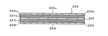
更に、電子回路装置20において、片面構造を有するフレキシブル配線板23の代わりに、図9に示すような、いわゆる両面構造を有するフレキシブル配線板23Aが採用されてもよい。図9に示すフレキシブル配線板23Aは、ポリイミド樹脂といった樹脂により形成されたベースフィルム230と、このベースフィルム230の一方の面に接着剤層231uを介して貼着された銅箔等からなる配線用導体232uと、ベースフィルム230の他方の面に接着剤層231lを介して貼着もしくは直接溶着された銅箔等からなる配線用導体232lと、配線用導体232uやベースフィルム230に対して接着剤層233uを介して貼着されて配線用導体232uを覆うカバーフィルム(第1のカバーフィルム)234uと、配線用導体232lやベースフィルム230に対して接着剤層233lを介して貼着されて配線用導体232lを覆うカバーフィルム(第2のカバーフィルム)234lとを含むものである。
このような両面構造を有するフレキシブル配線板23Aを採用する場合には、図10に示すように、フレキシブル配線板23Aに対して、接続端子236に接続される配線用導体232uと放熱プレート24側の配線用導体232l(あるいは配線としては利用されない銅箔)とを熱的に接続する熱伝導用ビア239をベースフィルム230と同層に配置すると共に、放熱プレート24側の配線用導体232lと熱的に接続される熱伝導用パッド(伝熱材)238を放熱プレート24側のカバーフィルム234lから露出するように設けるとよい。これにより、放熱プレート24の開口24o内にパルスヒータHを挿入すると共にパルスヒータHの先端を熱伝導用パッド238に押し当てれば、片面構造を有するフレキシブル配線板23に比べて厚みがある両面構造を有するフレキシブル配線板23Aを用いた場合であっても、ボンディング材27に対して良好に熱を伝えて接続端子26と接続端子236との接続処理を容易かつ効率よく実行することが可能となる。
図11は、変形例に係る電子回路装置20Bを示す平面図であり、図12は、図11のXII-XII線に沿った断面図である。これらの図面に示す電子回路装置20Bでは、回路基板22Bの実装面に複数の接続端子26が並設されると共に、片面構造を有するフレキシブル配線板23Bのベースフィルム230側、すなわち回路基板22Bとの接着面とは反対側の面に複数の接続端子236が並設されている。また、図11に示すように、電子回路装置20Bに含まれるフレキシブル配線板23Bにおいて、互いに隣り合う接続端子26同士の間に延在するスリットは図1等に例示したフレキシブル配線板23に比べて長く形成されており、それにより各遊端部23fの長さが図1等に例示したフレキシブル配線板23のものに比べて長くなっている。更に、電子回路装置20Bの放熱プレート24Bには、開口が形成されていない。そして、回路基板22Bの接続端子26とそれに対応したフレキシブル配線板23Bの接続端子236とは、図12に示すように、複数の遊端部23fがそれぞれ回路基板22B上に乗り上げる状態で電気的に接続されている。このような構造を有する電子回路装置20Bにおいても、回路基板22Bや放熱プレート24Bに振動が作用したり熱衝撃が加えられたりしたときに、回路基板22Bの接続端子236との接続部周辺でフレキシブル配線板23Bに作用する応力を緩和することができる。また、図12に示すようにフレキシブル配線板23Bの遊端部23fに撓みをもたせることで、応力緩和をより効果的に図ることが可能となる。
変形例に係る電子回路装置20Bを製造するに際しては、電子部品21が実装された回路基板22Bと、複数の接続端子236や複数の遊端部23f、スペーサ部23sを有するフレキシブル配線板23Bと、開口を有さない放熱プレート24Bとを用意した上で、まず、フレキシブル配線板23Bのベースフィルム230と放熱プレート24Bとを放熱接着剤により互いに接着する。この際、フレキシブル配線板23Bの各遊端部23f(ベースフィルム230)と放熱プレート24Bとは放熱接着剤により接着されないが、フレキシブル配線板23Bの各スペーサ部23s(ベースフィルム230)と放熱プレート24Bとは放熱接着剤を介して互いに接着される。
次いで、フレキシブル配線板23Bの各遊端部23fが回路基板22B上に乗り上げると共に回路基板22Bの各接続端子26がフレキシブル配線板23Bの対応する接続端子236と対向するようにしながら、回路基板22Bの非実装面とフレキシブル配線板23のカバーフィルム234とを放熱接着剤により接着すると共に、回路基板22Bの非実装面と放熱プレート24Bとをフレキシブル配線板23Bの開口23o内に配置した放熱接着剤により接着する。この際、互いに対向し合う回路基板22Bの接続端子26とフレキシブル配線板23Bの接続端子236との間には、ACF(Anisotropic Condactive Film)等のボンディング材を配置する。また、回路基板22Bとフレキシブル配線板23Bとの接着に際して、回路基板22Bとフレキシブル配線板23Bの各遊端部23fとは放熱接着剤により接着されないが、回路基板22Bとフレキシブル配線板23Bの各スペーサ部23s(カバーフィルム234)とは放熱接着剤を介して互いに接着される。
回路基板22Bをフレキシブル配線板23Bや放熱プレート24Bに対して接着したならば、接続端子236の上方からパルスヒータの先端をフレキシブル配線板23Bのカバーフィルム234に押し当て、パルスヒートによりボンディング材を加熱溶融させて互いに対向し合う接続端子26と接続端子236とを電気的に接続する。この場合、配線用導体232を介して接続端子236と熱的に接続される図示しない熱伝導用パッドをカバーフィルム234から露出するように設けておき、当該熱伝導用パッドにパルスヒータを押し当てるようにしてもよい。そして、互いに接着されて一体化した回路基板22B、フレキシブル配線板23Bおよび放熱プレート24Bを金型内にセットし、トランスファーモールド成形により封止樹脂部25aおよび25bを成形する。
また、図13に示すように、変形例の電子回路装置20Bにおいて、片面構造を有するフレキシブル配線板23Bの代わりに、図9に例示したような、いわゆる両面構造を有するフレキシブル配線板23Cが採用されてもよい。両面構造を有するフレキシブル配線板23Cを採用する場合には、フレキシブル配線板23Cに対して、接続端子236に接続される放熱プレート24B側の配線用導体232lと図中上側の配線用導体232u(あるいは配線としては利用されない銅箔)とを熱的に接続する熱伝導用ビア239をベースフィルム230と同層に配置すると共に、図中上側の配線用導体232uと熱的に接続される熱伝導用パッド(伝熱材)238を図中上側のカバーフィルム234uから露出するように設けるとよい。これにより、パルスヒータHの先端を熱伝導用パッド238に押し当てれば、片面構造を有するフレキシブル配線板23に比べて厚みがある両面構造を有するフレキシブル配線板23Cを用いた場合であっても、ボンディング材に対して良好に熱を伝えて接続端子26と接続端子236との接続処理を容易かつ効率よく実行することが可能となる。
更に、図13に示すように、回路基板22の非実装面に各接続端子26と対向するように熱伝導用パッド28を配置すると共に、熱伝導用パッド28とそれに対応する接続端子26とを熱伝導用ビア29を介して熱的に接続しておいてもよい。これにより、回路基板22の接続端子26とフレキシブル配線板23の接続端子236とを電気的に接続するに際して、放熱プレート24BにホットプレートHPを押し当てることにより、フレキシブル配線板23C側のみならず放熱プレート24B側からもボンディング材27に対して熱を付与することが可能となるので、接続端子26と接続端子236との電気的接続を速やかに実現すると共に、両者をより確実に電気的に接続することができる。
なお、実施例の電子回路装置20および20Bでは、回路基板22の非実装面とフレキシブル配線板23とが接着されているが、回路基板22とフレキシブル配線板23とを互いに接着することなく、回路基板22を放熱プレート24にのみ接着すると共にフレキシブル配線板23を放熱プレート24にのみ接着してもよい。また、上記電子回路装置20および20Bは、回路基板22とフレキシブル配線板23の一部と放熱プレート24の一部とを封止するようにモールド成形された樹脂からなる封止樹脂部25a,25bを有するものであるが、電子回路装置20等は、封止樹脂部の代わりに、回路基板22やフレキシブル配線板23の一部を覆うカバーを有するものとして構成されてもよいことはいうまでもない。更に、上述の電子回路装置20等は、車両用自動変速機を制御するのに用いられるものとして説明されたが、これに限られるものではない。すなわち、電子回路装置20等は、例えば内燃機関や電動機といった他の車載機器を制御する電子制御ユニットとして構成されてもよく、車載機器以外の機器を制御等する電子回路装置として構成されてもよい。
ここで、実施例や変形例の主要な要素の欄に記載した発明の主要な要素との対応関係について説明する。すなわち、実施例や変形例において、電子部品21が実装された回路基板22,22Bが「回路基板」に相当し、回路基板22等と外部機器100との電気的接続を可能とするフレキシブル配線板23,23A,23B,23Cが「フレキシブル配線板」に相当し、回路基板22の実装面または非実装面に並設された接続端子26が「回路側接続端子」に相当し、回路基板22の複数の接続端子26と対向するようにフレキシブル配線板23等の表裏面の何れか一方に並設された接続端子236が「配線板側接続端子」に相当し、それぞれ少なくとも1つの接続端子236を含むように形成された遊端部23fが「遊端部」に相当し、フレキシブル配線板23等に接着された放熱プレート24、24Bが「放熱部材」に相当し、回路基板22等とフレキシブル配線板23等の一部と放熱プレート24等の一部とを封止するように成形された樹脂からなる封止樹脂部25a,25bが「封止樹脂部」に相当する。ただし、これら実施例および変形例の主要な要素の欄に記載した発明の主要な要素との対応関係は、実施例が記載した発明を実施するための最良の形態を具体的に説明するための一例であることから、記載した発明の要素を限定するものではない。すなわち、実施例はあくまで記載した発明の具体的な一例に過ぎず、記載した発明の解釈は、その欄の記載に基づいて行なわれるべきものである。
以上、実施例を用いて本発明の実施の形態について説明したが、本発明は上記実施例に何ら限定されるものではなく、本発明の要旨を逸脱しない範囲内において、様々な変更をなし得ることはいうまでもない。
本発明は、電子回路装置の製造産業において利用可能である。
Claims (8)
- 電子部品が実装された回路基板と、該回路基板と外部機器との電気的接続を可能とするフレキシブル配線板とを含む電子回路装置であって、
前記回路基板は、前記電子部品が実装される実装面または該実装面とは反対側の面である非実装面に並設された複数の回路側接続端子を有し、
前記フレキシブル配線板は、前記回路基板の前記複数の回路側接続端子と対向するように表面および裏面の何れか一方に並設された複数の配線板側接続端子と、それぞれ少なくとも1つの前記配線板側接続端子を含むように形成された複数の遊端部とを有し、
前記フレキシブル配線板の前記遊端部は前記回路基板に接着されず、前記回路側接続端子とそれに対応した前記配線板側接続端子とが互いに対向し合う状態で電気的に接続されることを特徴とする電子回路装置。 - 請求項1に記載の電子回路装置において、
前記フレキシブル配線板の前記遊端部は、前記配線板側接続端子の並設方向に延びるように前記フレキシブル配線板に形成された第1のスリットと、互いに隣り合う前記配線板側接続端子同士の間で前記第1のスリットから前記並設方向と概ね直交する方向に少なくとも前記配線板側接続端子を超える位置まで延びるように前記フレキシブル配線板に形成された複数の第2のスリットとにより画成されることを特徴とする電子回路装置。 - 請求項1に記載の電子回路装置において、
前記フレキシブル配線板の前記遊端部以外の部位に対して前記回路基板とは反対側から接着された放熱部材を更に備え、
前記複数の回路側接続端子は、前記回路基板の前記非実装面に並設されており、
前記複数の配線板側接続端子は、前記フレキシブル配線板の前記放熱部材との接着面とは反対側の面に並設されており、
前記放熱部材には、前記フレキシブル配線板の前記複数の配線板側接続端子と対向するように開口が形成されていることを特徴とする電子回路装置。 - 請求項3に記載の電子回路装置において、
前記放熱部材の前記並設方向における両端部の少なくとも一部には、前記フレキシブル配線板が接着されないことを特徴とする電子回路装置。 - 請求項1に記載の電子回路装置において、
前記複数の回路側接続端子は、前記回路基板の前記実装面に並設されており、
前記複数の配線板側接続端子は、前記フレキシブル配線板の前記回路基板側とは反対側の面に並設されており、
前記回路側接続端子とそれに対応した前記配線板側接続端子とは、前記フレキシブル配線板の前記複数の遊端部がそれぞれ前記回路基板上に乗り上げる状態で電気的に接続されることを特徴とする電子回路装置。 - 請求項1に記載の電子回路装置において、
前記フレキシブル配線板は、前記配線板側接続端子に接続される配線用導体と、該配線用導体に対して前記配線板側接続端子とは反対側から熱的に接続される伝熱材と、前記配線板側接続端子を外部に露出させた状態で前記配線用導体の一方の面を覆う第1のカバーフィルムと、前記伝熱材を外部に露出させた状態で前記配線用導体の他方の面を覆う第2のカバーフィルムとを含むことを特徴とする電子回路装置。 - 請求項1に記載の電子回路装置において、
前記フレキシブル配線板には、前記回路基板の前記非実装面と対向するように開口が形成されており、前記回路基板の前記非実装面と前記放熱部材とは、前記開口内に形成される放熱接着剤の層を介して互いに接着されており、前記フレキシブル配線板は、前記開口と前記遊端部との間に前記回路基板と前記放熱部材とに接着されるスペーサ部を含むことを特徴とする電子回路装置。 - 請求項1に記載の電子回路装置において、
前記回路基板と前記フレキシブル配線板の一部を封止するようにモールド成形された樹脂からなる封止樹脂部を更に備えることを特徴とする電子回路装置。
Priority Applications (2)
| Application Number | Priority Date | Filing Date | Title |
|---|---|---|---|
| DE112010000032T DE112010000032T5 (de) | 2009-03-13 | 2010-01-29 | Elektronische Schaltungsvorrichtung |
| CN2010800031531A CN102210199B (zh) | 2009-03-13 | 2010-01-29 | 电子电路装置 |
Applications Claiming Priority (2)
| Application Number | Priority Date | Filing Date | Title |
|---|---|---|---|
| JP2009-060724 | 2009-03-13 | ||
| JP2009060724A JP5249096B2 (ja) | 2009-03-13 | 2009-03-13 | 電子回路装置 |
Publications (1)
| Publication Number | Publication Date |
|---|---|
| WO2010103875A1 true WO2010103875A1 (ja) | 2010-09-16 |
Family
ID=42728170
Family Applications (1)
| Application Number | Title | Priority Date | Filing Date |
|---|---|---|---|
| PCT/JP2010/051216 Ceased WO2010103875A1 (ja) | 2009-03-13 | 2010-01-29 | 電子回路装置 |
Country Status (5)
| Country | Link |
|---|---|
| US (1) | US8279612B2 (ja) |
| JP (1) | JP5249096B2 (ja) |
| CN (1) | CN102210199B (ja) |
| DE (1) | DE112010000032T5 (ja) |
| WO (1) | WO2010103875A1 (ja) |
Cited By (1)
| Publication number | Priority date | Publication date | Assignee | Title |
|---|---|---|---|---|
| DE102010039277A1 (de) * | 2010-08-12 | 2012-02-16 | Endress + Hauser Gmbh + Co. Kg | Leiterplatte und elektronisches Gerät mit einer solchen Leiterplatte |
Families Citing this family (11)
| Publication number | Priority date | Publication date | Assignee | Title |
|---|---|---|---|---|
| US8446556B2 (en) * | 2008-07-08 | 2013-05-21 | Sharp Kabushiki Kaisha | Flexible printed circuit and electric circuit structure |
| US20140118954A1 (en) * | 2011-06-28 | 2014-05-01 | Telefonaktiebolaget L M Ericsson (Publ) | Electronic device with heat-dissipating structure |
| JP2017503175A (ja) * | 2013-12-31 | 2017-01-26 | キヤノン ユー.エス. ライフ サイエンシズ, インコーポレイテッドCanon U.S. Life Sciences, Inc. | 現場配置可能な小型フォーマットの迅速一次結果マイクロ流体システム |
| JP6507056B2 (ja) * | 2015-07-24 | 2019-04-24 | 株式会社オートネットワーク技術研究所 | 電池配線モジュール |
| DE102015219072A1 (de) * | 2015-10-02 | 2017-04-06 | Robert Bosch Gmbh | Elektronikmodul für ein Getriebesteuergerät |
| DE102016209141A1 (de) * | 2016-05-25 | 2017-11-30 | Robert Bosch Gmbh | Elektronisches Steuermodul und Verfahren zur Herstellung eines elektronischen Steuermoduls |
| TWI743182B (zh) * | 2017-08-25 | 2021-10-21 | 易鼎股份有限公司 | 軟性電路板適應性接觸壓力的接觸結構 |
| CN108807359A (zh) * | 2018-07-26 | 2018-11-13 | 中山市光圣半导体科技有限责任公司 | 一种led器件及制造方法 |
| JP7264630B2 (ja) * | 2018-12-04 | 2023-04-25 | 新電元工業株式会社 | 電子モジュール |
| JP7225150B2 (ja) * | 2020-03-06 | 2023-02-20 | 株式会社東芝 | サスペンションアッセンブリおよびディスク装置 |
| DE102023104557A1 (de) * | 2023-02-23 | 2024-08-29 | Olympus Winter & Ibe Gmbh | Endoskop, gedruckte leiterplatte eines endoskops und verfahren zur elektrischen verbindung einer gedruckten leiterplatte mit einer baugruppe |
Citations (5)
| Publication number | Priority date | Publication date | Assignee | Title |
|---|---|---|---|---|
| JPH0513904A (ja) * | 1991-07-01 | 1993-01-22 | Canon Inc | フレキシブルプリント基板 |
| JP2000294604A (ja) * | 1999-04-07 | 2000-10-20 | Nec Corp | テープキャリアパッケージ |
| JP2006140273A (ja) * | 2004-11-11 | 2006-06-01 | Denso Corp | 電子制御装置およびその製造方法 |
| JP2006319265A (ja) * | 2005-05-16 | 2006-11-24 | Sharp Corp | プリント配線基板用表面実装部品取外し装置及び該表面実装部品取外し装置を使用可能なプリント配線基板並びに該プリント配線基板の表面実装部品取外し方法 |
| JP2007088228A (ja) * | 2005-09-22 | 2007-04-05 | Elpida Memory Inc | 積層型半導体装置及びその製造方法 |
Family Cites Families (5)
| Publication number | Priority date | Publication date | Assignee | Title |
|---|---|---|---|---|
| US4795079A (en) * | 1985-03-29 | 1989-01-03 | Canon Kabushiki Kaisha | Structure of joining printed circuit boards and process for producing the same |
| JP2678958B2 (ja) * | 1992-03-02 | 1997-11-19 | カシオ計算機株式会社 | フィルム配線基板およびその製造方法 |
| JP2003133677A (ja) * | 2001-10-29 | 2003-05-09 | Advanced Display Inc | フレキシブル回路基板の圧着構造 |
| JP3840180B2 (ja) * | 2002-12-26 | 2006-11-01 | 住友電工プリントサーキット株式会社 | フレキシブルプリント配線板 |
| JP4607612B2 (ja) * | 2005-02-09 | 2011-01-05 | 日東電工株式会社 | 配線回路基板およびその製造方法 |
-
2009
- 2009-03-13 JP JP2009060724A patent/JP5249096B2/ja active Active
-
2010
- 2010-01-29 WO PCT/JP2010/051216 patent/WO2010103875A1/ja not_active Ceased
- 2010-01-29 CN CN2010800031531A patent/CN102210199B/zh not_active Expired - Fee Related
- 2010-01-29 DE DE112010000032T patent/DE112010000032T5/de not_active Withdrawn
- 2010-03-08 US US12/719,331 patent/US8279612B2/en not_active Expired - Fee Related
Patent Citations (5)
| Publication number | Priority date | Publication date | Assignee | Title |
|---|---|---|---|---|
| JPH0513904A (ja) * | 1991-07-01 | 1993-01-22 | Canon Inc | フレキシブルプリント基板 |
| JP2000294604A (ja) * | 1999-04-07 | 2000-10-20 | Nec Corp | テープキャリアパッケージ |
| JP2006140273A (ja) * | 2004-11-11 | 2006-06-01 | Denso Corp | 電子制御装置およびその製造方法 |
| JP2006319265A (ja) * | 2005-05-16 | 2006-11-24 | Sharp Corp | プリント配線基板用表面実装部品取外し装置及び該表面実装部品取外し装置を使用可能なプリント配線基板並びに該プリント配線基板の表面実装部品取外し方法 |
| JP2007088228A (ja) * | 2005-09-22 | 2007-04-05 | Elpida Memory Inc | 積層型半導体装置及びその製造方法 |
Cited By (1)
| Publication number | Priority date | Publication date | Assignee | Title |
|---|---|---|---|---|
| DE102010039277A1 (de) * | 2010-08-12 | 2012-02-16 | Endress + Hauser Gmbh + Co. Kg | Leiterplatte und elektronisches Gerät mit einer solchen Leiterplatte |
Also Published As
| Publication number | Publication date |
|---|---|
| US8279612B2 (en) | 2012-10-02 |
| CN102210199B (zh) | 2013-09-25 |
| CN102210199A (zh) | 2011-10-05 |
| US20100232115A1 (en) | 2010-09-16 |
| JP5249096B2 (ja) | 2013-07-31 |
| DE112010000032T5 (de) | 2012-07-26 |
| JP2010219090A (ja) | 2010-09-30 |
Similar Documents
| Publication | Publication Date | Title |
|---|---|---|
| JP5249096B2 (ja) | 電子回路装置 | |
| JP5051189B2 (ja) | 電子回路装置 | |
| CN108370142B (zh) | 电路结构体及电气接线盒 | |
| KR950002544A (ko) | 다층금속프린트기판과 몰드모듈 | |
| CN101459156B (zh) | 半导体器件 | |
| US7080445B2 (en) | Method for connecting printed circuit boards and connected printed circuit boards | |
| US5423119A (en) | Method for manufacturing a hybrid circuit charge-coupled device image sensor | |
| CN106031313B (zh) | 电子控制模块及电子控制模块的制造方法 | |
| JP2004179309A (ja) | プリント回路基板の放熱構造とその製造方法 | |
| JPH07240496A (ja) | 半導体装置、その製造方法、半導体素子のテスト方法、そのテスト基板およびそのテスト基板の製造方法 | |
| JP2014531009A (ja) | 挿入される回路支持体と囲繞側回路支持体との間に複数のはんだ付けブリッジ若しくは常温接点を備えた変速機制御モジュール | |
| CN107006126B (zh) | 利用按压接触三明治模块技术的特别是用于机动车传动装置控制设备的电子装置模块 | |
| JP2010073851A (ja) | 半導体装置 | |
| JP4854770B2 (ja) | プリント基板ユニット及び電子機器 | |
| US20110199735A1 (en) | Substrate connecting structure and electronic device | |
| JP4407067B2 (ja) | 電子装置 | |
| CN107535060A (zh) | 电子组件、尤其是用于传动装置控制模块的电子组件 | |
| KR20140019751A (ko) | 밀봉 배치되는 소자들을 포함하는 샌드위치 구조의 자동차 변속기의 변속기 제어 모듈 | |
| KR100748558B1 (ko) | 칩 사이즈 패키지 및 그 제조 방법 | |
| JP2019036678A (ja) | 電子装置 | |
| JP2013105792A5 (ja) | ||
| JP2010219091A (ja) | 電子回路装置 | |
| JP2010219093A (ja) | 電子回路装置 | |
| JP2005051143A (ja) | スタックメモリ及びその製造方法 | |
| JP5679266B2 (ja) | プリント配線板の接続構造、配線板接続体及び電子機器 |
Legal Events
| Date | Code | Title | Description |
|---|---|---|---|
| WWE | Wipo information: entry into national phase |
Ref document number: 201080003153.1 Country of ref document: CN |
|
| 121 | Ep: the epo has been informed by wipo that ep was designated in this application |
Ref document number: 10750631 Country of ref document: EP Kind code of ref document: A1 |
|
| WWE | Wipo information: entry into national phase |
Ref document number: 1120100000328 Country of ref document: DE |
|
| 122 | Ep: pct application non-entry in european phase |
Ref document number: 10750631 Country of ref document: EP Kind code of ref document: A1 |