WO2010101104A1 - 超音波送受信回路、超音波診断装置 - Google Patents
超音波送受信回路、超音波診断装置 Download PDFInfo
- Publication number
- WO2010101104A1 WO2010101104A1 PCT/JP2010/053214 JP2010053214W WO2010101104A1 WO 2010101104 A1 WO2010101104 A1 WO 2010101104A1 JP 2010053214 W JP2010053214 W JP 2010053214W WO 2010101104 A1 WO2010101104 A1 WO 2010101104A1
- Authority
- WO
- WIPO (PCT)
- Prior art keywords
- ultrasonic
- transmission
- signal
- terminal
- circuit
- Prior art date
- Legal status (The legal status is an assumption and is not a legal conclusion. Google has not performed a legal analysis and makes no representation as to the accuracy of the status listed.)
- Ceased
Links
Images


Classifications
-
- G—PHYSICS
- G01—MEASURING; TESTING
- G01S—RADIO DIRECTION-FINDING; RADIO NAVIGATION; DETERMINING DISTANCE OR VELOCITY BY USE OF RADIO WAVES; LOCATING OR PRESENCE-DETECTING BY USE OF THE REFLECTION OR RERADIATION OF RADIO WAVES; ANALOGOUS ARRANGEMENTS USING OTHER WAVES
- G01S7/00—Details of systems according to groups G01S13/00, G01S15/00, G01S17/00
- G01S7/52—Details of systems according to groups G01S13/00, G01S15/00, G01S17/00 of systems according to group G01S15/00
- G01S7/52017—Details of systems according to groups G01S13/00, G01S15/00, G01S17/00 of systems according to group G01S15/00 particularly adapted to short-range imaging
- G01S7/52079—Constructional features
-
- A—HUMAN NECESSITIES
- A61—MEDICAL OR VETERINARY SCIENCE; HYGIENE
- A61B—DIAGNOSIS; SURGERY; IDENTIFICATION
- A61B8/00—Diagnosis using ultrasonic, sonic or infrasonic waves
- A61B8/44—Constructional features of the ultrasonic, sonic or infrasonic diagnostic device
- A61B8/4444—Constructional features of the ultrasonic, sonic or infrasonic diagnostic device related to the probe
-
- A—HUMAN NECESSITIES
- A61—MEDICAL OR VETERINARY SCIENCE; HYGIENE
- A61B—DIAGNOSIS; SURGERY; IDENTIFICATION
- A61B8/00—Diagnosis using ultrasonic, sonic or infrasonic waves
- A61B8/56—Details of data transmission or power supply
-
- G—PHYSICS
- G01—MEASURING; TESTING
- G01N—INVESTIGATING OR ANALYSING MATERIALS BY DETERMINING THEIR CHEMICAL OR PHYSICAL PROPERTIES
- G01N29/00—Investigating or analysing materials by the use of ultrasonic, sonic or infrasonic waves; Visualisation of the interior of objects by transmitting ultrasonic or sonic waves through the object
- G01N29/22—Details, e.g. general constructional or apparatus details
- G01N29/24—Probes
-
- G—PHYSICS
- G01—MEASURING; TESTING
- G01S—RADIO DIRECTION-FINDING; RADIO NAVIGATION; DETERMINING DISTANCE OR VELOCITY BY USE OF RADIO WAVES; LOCATING OR PRESENCE-DETECTING BY USE OF THE REFLECTION OR RERADIATION OF RADIO WAVES; ANALOGOUS ARRANGEMENTS USING OTHER WAVES
- G01S7/00—Details of systems according to groups G01S13/00, G01S15/00, G01S17/00
- G01S7/52—Details of systems according to groups G01S13/00, G01S15/00, G01S17/00 of systems according to group G01S15/00
- G01S7/52017—Details of systems according to groups G01S13/00, G01S15/00, G01S17/00 of systems according to group G01S15/00 particularly adapted to short-range imaging
-
- G—PHYSICS
- G10—MUSICAL INSTRUMENTS; ACOUSTICS
- G10K—SOUND-PRODUCING DEVICES; METHODS OR DEVICES FOR PROTECTING AGAINST, OR FOR DAMPING, NOISE OR OTHER ACOUSTIC WAVES IN GENERAL; ACOUSTICS NOT OTHERWISE PROVIDED FOR
- G10K11/00—Methods or devices for transmitting, conducting or directing sound in general; Methods or devices for protecting against, or for damping, noise or other acoustic waves in general
- G10K11/18—Methods or devices for transmitting, conducting or directing sound
- G10K11/26—Sound-focusing or directing, e.g. scanning
- G10K11/34—Sound-focusing or directing, e.g. scanning using electrical steering of transducer arrays, e.g. beam steering
- G10K11/341—Circuits therefor
-
- A—HUMAN NECESSITIES
- A61—MEDICAL OR VETERINARY SCIENCE; HYGIENE
- A61B—DIAGNOSIS; SURGERY; IDENTIFICATION
- A61B8/00—Diagnosis using ultrasonic, sonic or infrasonic waves
- A61B8/54—Control of the diagnostic device
-
- B—PERFORMING OPERATIONS; TRANSPORTING
- B06—GENERATING OR TRANSMITTING MECHANICAL VIBRATIONS IN GENERAL
- B06B—METHODS OR APPARATUS FOR GENERATING OR TRANSMITTING MECHANICAL VIBRATIONS OF INFRASONIC, SONIC, OR ULTRASONIC FREQUENCY, e.g. FOR PERFORMING MECHANICAL WORK IN GENERAL
- B06B2201/00—Indexing scheme associated with B06B1/0207 for details covered by B06B1/0207 but not provided for in any of its subgroups
- B06B2201/70—Specific application
- B06B2201/76—Medical, dental
-
- G—PHYSICS
- G01—MEASURING; TESTING
- G01N—INVESTIGATING OR ANALYSING MATERIALS BY DETERMINING THEIR CHEMICAL OR PHYSICAL PROPERTIES
- G01N2291/00—Indexing codes associated with group G01N29/00
- G01N2291/10—Number of transducers
- G01N2291/106—Number of transducers one or more transducer arrays
Definitions
- the present invention relates to an ultrasonic transmission / reception circuit that drives an ultrasonic probe and performs signal processing such as amplification of a received signal from the ultrasonic probe, and an ultrasonic diagnostic apparatus using the ultrasonic transmission / reception circuit.
- the ultrasonic diagnostic apparatus transmits ultrasonic waves from the ultrasonic probe into the subject, and uses the reflected echo signals received by the ultrasonic probe to ultrasonically convert the ultrasonic image of the diagnostic part in the subject.
- the image forming unit is configured to display the configured ultrasonic image on the display unit.
- the ultrasonic probe transmits an ultrasonic wave to a subject by driving a plurality of transducers built in an ultrasonic transmission circuit of the ultrasonic transmission / reception unit, and receives an ultrasonic wave of the ultrasonic transmission / reception unit.
- a reflected echo signal from the subject is received by the vibrator by the circuit.
- the ultrasonic transmission circuit is applied and driven to a plurality of transducers of the ultrasonic probe, and performs received signal processing such as amplifying the reflected echo signal.
- the transmission functions to apply a sine wave or rectangular wave signal to a plurality of transducers of the ultrasonic probe and drive it.
- the voltage level of the signal during transmission is, for example, a voltage level of 100 Vpp and a frequency of about several MHz to 20 MHz.
- the reception functions so that the reflected echo signal received by the ultrasonic probe is transmitted as an electrical signal, and the transmitted electrical signal is amplified.
- the voltage level of the reflected echo signal at the time of reception is several hundred mVpp or less, and the voltage level at the time of reception is about 1000 times different from the voltage level at the time of transmission.
- the ultrasonic transmission circuit and the ultrasonic reception circuit are constituted by respective circuit elements. Furthermore, a transmission / reception separating circuit for separating the ultrasonic transmitting circuit from the ultrasonic receiving circuit to electrically protect the ultrasonic receiving circuit has been provided. Therefore, the ultrasonic transmission / reception unit includes an ultrasonic transmission circuit, an ultrasonic reception circuit, and a transmission / reception separation circuit, and the circuit scale of the ultrasonic transmission / reception unit is large.
- Patent Document 1 An ultrasonic diagnostic apparatus having a switch that switches connection and disconnection from a power source used for a reception signal amplifier instead of a transmission / reception separation circuit. ing.
- An object of the present invention is to provide an ultrasonic transmission / reception circuit capable of reducing the circuit scale of an ultrasonic transmission / reception unit as compared with the prior art.
- Another object of the present invention is to provide an ultrasonic diagnostic apparatus capable of reducing the circuit scale of an ultrasonic transmission / reception unit as compared with the prior art.
- an ultrasonic transmission / reception circuit of the present invention includes a first terminal for a plurality of transducer elements constituting an ultrasonic probe, a second terminal connected to a transmission signal generation circuit, and the vibration. It has at least three terminals of the third terminal as the amplifier output terminal of the received signal from the child element, and the signal input to one terminal is amplified at the other terminal between the two terminals of the at least three terminals.
- a semiconductor circuit element having a function of outputting the first output, a first function that causes the semiconductor circuit element to function as an input switch for a transmission signal to the vibrator element, and a second that amplifies a reception signal received from the vibrator element And a control unit that controls the functions to function.
- the control unit since the control unit causes the semiconductor circuit element to function as the first function and the second function, respectively, the circuit scale of the ultrasonic transmission / reception unit can be reduced more than conventional. Can be planned.
- the ultrasonic diagnostic apparatus of the present invention drives an ultrasonic probe that transmits and receives ultrasonic waves to a subject, the ultrasonic probe, and the ultrasonic wave
- An ultrasonic transmission / reception unit that processes a reflected echo signal received from the probe, an ultrasonic image configuration unit that forms an ultrasonic image using the signal-processed reflected echo signal, and displays the ultrasonic image
- An ultrasonic diagnostic apparatus comprising: a display unit; a control unit that controls each unit of the ultrasonic probe or the display unit; and a setting unit that sets a control condition of each unit in the control unit,
- the ultrasonic transmission / reception unit includes a first terminal connected to a plurality of transducer elements constituting the ultrasonic probe, a second terminal connected to a transmission signal generation circuit, and an amplifier output end of a reception signal from the transducer element; Having at least three terminals of the third terminal, the at least Between two terminals of the three terminals, a semiconductor circuit element having a function
- the control unit since the control unit causes the semiconductor circuit element to function as the first function and the second function, respectively, the circuit scale of the ultrasonic transmission / reception unit can be reduced more than conventional. Can be planned.
- an ultrasonic transmission / reception circuit capable of reducing the circuit scale of the ultrasonic transmission / reception unit and an ultrasonic diagnostic apparatus using the same.
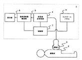
- FIG. 1 is a block diagram showing a configuration of an ultrasonic diagnostic apparatus to which the present invention is applied.
- 1 is a circuit configuration diagram and an operation diagram of Embodiment 1 of the present invention.
- FIG. 6 is a circuit configuration diagram and an operation diagram of Embodiment 3 of the present invention.
- FIG. 1 is a block diagram showing a configuration of an ultrasonic diagnostic apparatus to which the present invention is applied.
- the ultrasonic diagnostic apparatus 1 forms and displays an ultrasonic image of a diagnostic region using a reflected echo signal obtained by transmitting and receiving ultrasonic waves in the body of the subject 2.
- the ultrasonic diagnostic apparatus 1 includes an ultrasonic probe (abbreviated as a probe in FIG. 1) 3, an ultrasonic transmission / reception unit 4, an ultrasonic image configuration unit 5, a display unit 6, and a control unit. 7 and a control panel 8 are provided.
- the ultrasonic probe 3 irradiates the subject 2 with ultrasonic waves and receives a reflected echo signal from the subject 2, and has a multi-channel transducer element.
- the ultrasonic transmission / reception unit 4 functions as an ultrasonic transmission unit that drives the ultrasonic probe 3 to irradiate an ultrasonic signal, and an ultrasonic reception unit that amplifies the reflected echo signal received by the ultrasonic probe 3 With both functions.
- the ultrasonic image constructing unit 5 constructs an ultrasonic image based on the received signal.
- the display unit 6 displays the ultrasonic image configured in the ultrasonic image configuration unit 5.
- the control unit 7 is, for example, a CPU of a computer system that controls each element of the ultrasonic probe 3, the ultrasonic transmission / reception unit 4, the ultrasonic image configuration unit 5, and the display unit 6.
- the control panel 8 is a keyboard or a pointing device that the examiner gives control parameters to the control unit 7.
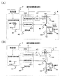
- FIG. 2 is a circuit configuration diagram and an operation diagram of the first embodiment of the present invention.
- FIG. 2 (A) shows an operation diagram during ultrasonic transmission
- FIG. 2 (B) shows an operation diagram during ultrasonic reception.
- the ultrasonic transmission / reception unit 4 includes a transmission signal generation unit 41, a phasing circuit 42, a field effect transistor (FET) 43, a high voltage switch (HVSW) 44, a constant current source 45, a gain adjustment circuit 46, and an analog-digital converter (ADC). 47).
- FET field effect transistor
- HVSW high voltage switch
- ADC analog-digital converter
- the transmission signal generator 41 generates a transmission signal to be supplied to each channel of the transducer element of the ultrasonic probe.
- the transmission signal is an arbitrary AC signal such as a rectangular wave signal.
- the transmission signal generation unit 41 receives a signal in a state where the ultrasonic wave is being transmitted or a signal in a reception state from the control unit 7, and supplies an AC signal to the gate terminal of the FET 43 at the time of transmission.
- a DC signal is supplied to the gate terminal of the FET 43 during reception.
- the transmission signal generator 41 may be configured by a memory such as a ROM that generates a transmission waveform.
- the phasing circuit 42 focuses the ultrasonic signal (reflected echo signal) at a depth for obtaining the ultrasonic image of the subject desired by the examiner.
- the transmission phasing circuit 421 and the reception phasing circuit 422 Have.
- the depth is set on the control panel 8, for example.
- the transmission phasing circuit 421 focuses the ultrasonic signal to be transmitted, and the reception phasing circuit 422 focuses the reflected echo signal.
- the phasing method of the phasing circuit 42 is either an analog phasing method for phasing an ultrasonic signal as an analog signal or a digital phasing method for digitizing an ultrasonic signal that is an analog signal by an ADC. May be.
- a typical example of the phasing circuit 42 is disclosed in Japanese Patent Laid-Open No. 2008-264342.
- the digital data is phased.
- the FET 43 is an NMOS type that is advantageous for integration.
- the reason for selecting the NMOS FET 43 is that the carrier of the NMOS FET is an electron and the effective mass is smaller than that of the PMOS hole, so that the carrier moves fast, that is, it can operate at high speed, and the FET element itself
- the occupation area is also smaller for the NMOS type than for the PMOS type.
- the case where the NMOS type is used will be described.
- substantially the same function as the case where the NMOS type is used is the same as the complementary type using the PMOS type or a mixture of the NMOS type and the PMOS type. It can be realized even if it is used.
- the FET 43 receives an input from its own gate terminal, inputs an AC voltage indicated by a sine wave or a rectangular wave to the gate terminal at the time of transmission, and transmits the transducer constituting the ultrasonic probe 3 from its own source terminal. Functions to output AC voltage to one channel (first function). Since the FET 43 constitutes a source follower circuit, the transmission waveform applied to the gate terminal is output to the source terminal as it is. The feature of the source follower circuit is that the input impedance is high and the output impedance is low. If the input impedance is high, the effect of using the circuit is reduced, and if the output impedance is low, more loads (vibrators) can be driven.
- the FET 43 receives the input of its own gate terminal, and upon reception, inputs a DC voltage to the gate terminal, inputs the reflected echo signal output from the transducer 1 channel to its source terminal, and itself It becomes an amplifier element of the ground amplifier circuit, and functions so that the amplified reflected echo signal is output from its drain terminal to the ADC 47 (second function).
- the gain of the grounded-gate amplifier is substantially expressed by Equation 1 as the product of the equivalent conductance gm of the FET 43 itself and the variable resistor Rd in the gain adjustment circuit 46.
- the gate-grounded amplifier circuit fixes the voltage of the gate terminal of the FET 43 to a constant DC voltage (also referred to as a “bias voltage”), uses the source terminal of the FET 43 as an input terminal of the signal to be amplified, and connects the load resistor Rd to the FET 43.
- the drain terminal is used as an output terminal for the amplified signal.
- the gain of the amplifier of the grounded-gate amplifier circuit can be changed by changing the value of the variable resistor Rd.
- the control unit 7 can control the value of the variable resistor Rd according to the display depth of the ultrasonic image of the subject.
- the gain of the amplifier of the grounded-gate amplifier circuit is proportional to the size of the variable resistor Rd.
- the high voltage switch (HVSW) 44 is a switch that is connected to the source terminal of the FET 43 and supplies the output of one transmission signal generator 41 to a plurality of transducer elements in order to supply signals to all elements of the transducer. is there.
- the HVSW 44 is used when the total number of elements and circuits of the transducers in the driven probe are different.
- the transmission signal generation circuit 41 that supplies a transmission signal from the transmission phasing circuit 421 is replaced with the number of transducer elements, as will be described in the following specific example. Because it can be halved.
- transducer elements are arranged in a line in the left-right direction, and when the transducer elements are represented by symbols 31 to 38 in order from the left, one pair at both ends is 31 and 38, one element Consider that the inner pair is 32 and 37, the inner pair is 33 and 36, and the innermost pair is 34 and 35 (not shown). If the ultrasonic beams transmitted from the transducer elements only need to be line symmetric when viewed from the center of the array of transducer elements, the same transmission signal from the transmission signal generation circuit 41 is transmitted to each pair described above. It only has to be supplied. That is, the transmission signal generation circuit 41 does not need the same number of eight as the transducer elements, and only half of them is sufficient.
- the actual number of transducer elements becomes even larger, such as 96, 128, and 192 channels.
- the transducer elements are arranged in two dimensions. Since the actual number of transducer elements will further increase in the number of channels in the future, halving the number of transmission signal generation circuits 41 further contributes to a reduction in circuit scale.
- the transducer element connected to the transmission circuit is switched every time the aperture is moved.
- the number of transmission circuits can be made smaller than the total number of transducer elements.
- the transmission signal generation circuit 41 in the row direction of the arrangement direction of the transducer elements is If also used, the number of transmission signal generation circuits 41 can be reduced by more than half the number of transducer elements arranged two-dimensionally. Thus, the reduction in the number of transmission signal generation circuits 41 further contributes to the reduction in circuit scale.
- the transmission signal generation circuits 41 may be prepared for all the transducer elements without using the HVSW 44.
- the constant current source 45 indicates that the current I is held constant regardless of the magnitude of the load impedance, and flows the DC component of the current flowing from the source terminal of the FET 43 to the negative power source (Vss) of the power source that supplies the FET 43 Acts as follows.
- the current source may be a current controlled voltage source.
- the gain adjustment circuit 46 has a function of adjusting the gain of the received signal and supplies it to the FET 43. It has a Zener diode ZD that connects the positive power supply (Vdd) of the power supply and its cathode terminal, and a variable resistor Rd that is connected in parallel to the cathode terminal and the anode terminal of the Zener diode ZD.
- the Zener diode ZD is an element that not only allows a current to flow in the forward direction like a normal diode, but also allows a current to flow in the reverse direction if the reverse voltage is greater than a rated breakdown voltage called a “Zener voltage”.
- a constant voltage circuit is formed using the characteristics of the Zener voltage.
- the variable resistor Rd is a resistor whose value can be varied by a signal from the control unit 7, and is a digital potentiometer, for example.
- the ADC 47 inputs the reflected echo signal amplified by the grounded-gate amplifier circuit including the FET 43 as an analog signal from the drain terminal of the FET 43, digitizes it, and outputs it as reflected echo data.
- the reflected echo data phased by the reception phasing circuit 422 is output to the ultrasonic image construction unit 5.
- the examiner uses the control panel 8 to set control parameters such as subject information such as the name of the subject and measurement information including a desired display depth.
- the control unit 7 controls each element of the ultrasonic probe 3, the ultrasonic transmission / reception unit 4, the ultrasonic image configuration unit 5, and the display unit 6 based on the set control parameters.
- each operation during ultrasonic transmission and during ultrasonic reception is repeated at a predetermined transmission / reception repetition frequency.
- the control unit 7 causes an AC voltage such as a sine wave or a rectangular wave to be input to the transmission phasing circuit 421 as the transmission signal 41a.
- the control unit 7 receives the set display depth of the desired subject and focuses the set transmission signal 41a by the transmission phasing circuit 421.
- the output from the transmission phasing circuit 421 is input to the gate terminal of the FET 43.
- An output signal from the source terminal of the FET 43 is transmitted to one channel of the transducer 3a constituting the ultrasonic probe.
- the vibrator 3a receives the transmitted signal, vibrates, and transmits ultrasonic waves to the subject.
- the control unit 7 inputs a DC voltage to the transmission phasing circuit 421 as a reception switching signal 41b. Since the transmission phasing circuit 421 is at the time of reception, it does not operate, and the DC voltage is directly input to the gate terminal of the FET 43.
- the FET 43 receives a DC voltage supplied to its gate terminal and functions as a grounded gate amplifier.
- the control unit 7 sets the gain of the FET 43 (gate grounded amplifier) in the variable resistor Rd of the gain adjustment circuit 46.
- the vibrator 3a receives a reflected echo signal from the subject.
- the received reflected echo signal is transmitted to the source terminal of the FET 43.
- the FET 43 amplifies the reflected echo signal transmitted to its source terminal by the gain obtained by the product of its own equivalent conductance gm and the variable resistor Rd in the gain adjustment circuit 46, and is amplified to its own drain terminal.
- the reflected echo signal is output to ADC47.
- the ADC 47 inputs the amplified reflected echo signal as an analog signal, digitizes it, and outputs it as reflected echo data.
- the control unit 7 receives the set desired display depth of the subject, and focuses the reflected echo data by the reception phasing circuit 422.
- the reflected echo data phased by the reception phasing circuit 422 is output to the ultrasonic image construction unit 5. Further, the ultrasonic image constructing unit 5 constructs an ultrasonic image based on the received signal. The display unit 6 displays the ultrasonic image configured in the ultrasonic image configuration unit 5.
- phasing is performed on both the transmission side and the reception side, but phasing may be performed on either the transmission side or the reception side.
- the FET 43 realizes the function of supplying the signal at the time of transmission to the transducer 3a and the function of amplifying the echo signal at the time of reception with one element.
- the circuit scale of the ultrasonic transmission / reception unit can be reduced as compared with the prior art.
- the unique effect of the first embodiment is that it can contribute to the reduction of the circuit scale in that the number of elements used as the main elements of the circuit can be reduced with the transmission signal generator 41, the FET 43, the gain adjustment circuit 46, and the ADC 47.
- FIG. 3 is a circuit configuration diagram and an operation diagram of the second embodiment of the present invention.
- FIG. 3 (A) is a modified diagram of FIG. 2
- FIG. 3 (B) shows an operation diagram at the time of ultrasonic transmission.
- the ultrasonic transmission / reception unit 4 includes the transmission signal generation unit 41, the phasing circuit 42, the FET 43, and the gain adjustment circuit 46 of the first embodiment, and an addition or change part includes a digital-analog converter (DAC) 48 and a current mirror.
- DAC digital-analog converter
- a circuit 49, a resistor 4A, and a differentiating circuit 4B are provided.
- DAC48 converts the digital data of the ultrasonic signal to be transmitted, which is focused by the digital phasing method, into an analog ultrasonic signal.
- the current mirror circuit 49 is connected to the DAC 48, and an ultrasonic signal having the same phase as that of the DAC 48 is output to the gate terminal of the FET 43. This is because the AC signal supplied to the gate terminal of the FET 43 is output as it is to the vibrator 3a, so that the output current as an element of the DAC 48 does not reach the drive current necessary for driving the vibrator 3a. . Therefore, the gate terminals of the input current side FET and the output current side FET of the current mirror circuit 49 are short-circuited to obtain a drive current necessary for driving the vibrator 3a with the output current side FET. Yes.
- Resistor 4A is provided for the purpose of biasing the output signal of the FET on the output current side of the current mirror circuit 49.
- the differentiation circuit 4B is provided at the source terminal of the FET 43, obtains a detection signal for causing a current to flow from the vibrator 3a only when the transmission signal falls, and transmits the detection signal to the control unit 7.
- the examiner uses the control panel 8 to set control parameters such as subject information such as the name of the subject and measurement information including a desired display depth.
- the control unit 7 controls each element of the ultrasonic probe 3, the ultrasonic transmission / reception unit 4, the ultrasonic image configuration unit 5, and the display unit 6 based on the set control parameters.
- each operation during ultrasonic transmission and during ultrasonic reception is repeated at a predetermined transmission / reception repetition frequency.
- the control unit 7 causes an AC voltage such as a sine wave or a rectangular wave to be input to the transmission phasing circuit 421 as the transmission signal 41a.
- the control unit 7 receives the set display depth of the desired subject and focuses the set transmission signal 41a by the transmission phasing circuit 421.
- the output from the transmission phasing circuit 421 is input to the gate terminal of the FET 43.
- An output signal from the source terminal of the FET 43 is transmitted to one channel of the transducer 3a constituting the ultrasonic probe.
- the vibrator 3a receives the transmitted signal, vibrates, and transmits ultrasonic waves to the subject.
- the current flows through the vibrator 3a from Vdd through the Zener diode ZD, through the drain terminal and the source terminal of the FET 43. .
- the current flows from the vibrator 3a to the FET 43 as in the first embodiment, but in this embodiment, transmission is performed by the differentiation circuit 4B provided at the source terminal of the FET 43. Only when the ultrasonic signal falls, current flows from the transducer 3a. Therefore, it is possible to suppress power consumption driven by the vibrator 3a as compared with the constant energization of the first embodiment.
- the control unit 7 inputs a DC voltage to the transmission phasing circuit 421 as a reception switching signal 41b. Since the transmission phasing circuit 421 is at the time of reception, it does not operate, and the DC voltage is directly input to the gate terminal of the FET 43.
- the FET 43 receives a DC voltage supplied to its gate terminal and functions as a grounded gate amplifier.
- the control unit 7 sets the gain of the FET 43 (gate grounded amplifier) in the variable resistor Rd of the gain adjustment circuit 46.
- the vibrator 3a receives a reflected echo signal from the subject.
- the received reflected echo signal is transmitted to the source terminal of the FET 43.
- the FET 43 amplifies the reflected echo signal transmitted to its source terminal by the gain obtained by the product of its own equivalent conductance gm and the variable resistor Rd in the gain adjustment circuit 46, and is amplified to its own drain terminal.
- the reflected echo signal is output to ADC47.
- the ADC 47 inputs the amplified reflected echo signal as an analog signal, digitizes it, and outputs it as reflected echo data.
- the control unit 7 receives the set display depth of the desired subject and focuses the reflected echo data on the transmission phasing circuit 421.
- the reflected echo data phased by the reception phasing circuit 422 is output to the ultrasonic image construction unit 5. Further, the ultrasonic image constructing unit 5 constructs an ultrasonic image based on the received signal. The display unit 6 displays the ultrasonic image configured in the ultrasonic image configuration unit 5.
- phasing is performed on both the transmission side and the reception side, but phasing may be performed on either the transmission side or the reception side.
- the FET 43 realizes the function of supplying the signal during transmission to the transducer 3a and the function of amplifying the echo signal during reception with a single element.
- the circuit scale of the ultrasonic transmission / reception unit can be reduced as compared with the prior art.
- the unique effect of the second embodiment is that the current flowing through the vibrator during transmission is turned on only when the transmission waveform falls, so that power consumption can be reduced. In other words, since heat generation from the circuit can be suppressed, the circuit elements can be arranged close to each other, which contributes to a reduction in circuit scale.
- Example 1 or Example 2 is realized with a single-stage FET, a withstand voltage to a high voltage is also required as an electrical characteristic.
- An example of measuring power saving by connecting FETs having a low voltage of about 5V in multiple stages will be described with reference to FIG.
- FIG. 4 is a circuit configuration diagram and an operation diagram of Embodiment 3 of the present invention.
- low voltage FET43-1, FET43-2, ..., FET43-n of about 5V are connected in multiple stages.
- a multi-stage connection method is Darlington connection which is performed to increase the current amplification factor of a transistor. Although gm does not increase even when a FET is connected in a Darlington connection, when used in a source follower circuit as in the present invention, the input impedance of an element connected as an output load of the FET can be lowered.
- the FET 43 realizes the function of supplying the signal at the time of transmission to the transducer 3a and the function of amplifying the echo signal at the time of reception with one element.
- the circuit scale of the ultrasonic transmission / reception unit can be reduced as compared with the prior art.
- the special effect of the third embodiment is that during reception, application of Vdd and Vss power supply can be stopped and operation can be performed with a low voltage power supply of about 5V.
- the receiving circuit can be configured with an FET having a lower withstand voltage.
- the multi-stage FET is connected in Darlington, so that the input impedance of the element connected as the output load of the FET can be lowered, so that the noise of the grounded-gate amplifier can be kept low.
- the semiconductor circuit element has been described as a field effect transistor, but it has at least three terminals such as a bipolar transistor, and has a function of amplifying an electric signal between any two terminals. Any semiconductor circuit element can be implemented.
- a bipolar transistor When a bipolar transistor is used as a semiconductor circuit element, for example, a collector terminal is connected to a plurality of transducer elements constituting an ultrasonic probe, a transmission signal generating circuit is connected to a base terminal, and an emitter terminal is What is necessary is just to make it the amplifier output terminal of the received signal from a child element.
- the transducer of the ultrasonic probe may be a piezoelectric element or a CMUT (Capacitive Micro-Machined Ultrasonic Transducer).
- the present invention can be applied to an ultrasonic diagnostic apparatus for medical use and animal husbandry, and can also be applied to an ultrasonic flaw detection apparatus for nondestructive inspection.
Landscapes
- Engineering & Computer Science (AREA)
- Physics & Mathematics (AREA)
- Health & Medical Sciences (AREA)
- Life Sciences & Earth Sciences (AREA)
- General Physics & Mathematics (AREA)
- Computer Networks & Wireless Communication (AREA)
- Radar, Positioning & Navigation (AREA)
- Remote Sensing (AREA)
- General Health & Medical Sciences (AREA)
- Pathology (AREA)
- Biophysics (AREA)
- Medical Informatics (AREA)
- Veterinary Medicine (AREA)
- Public Health (AREA)
- Animal Behavior & Ethology (AREA)
- Nuclear Medicine, Radiotherapy & Molecular Imaging (AREA)
- Radiology & Medical Imaging (AREA)
- Biomedical Technology (AREA)
- Heart & Thoracic Surgery (AREA)
- Surgery (AREA)
- Molecular Biology (AREA)
- Biochemistry (AREA)
- Chemical & Material Sciences (AREA)
- Analytical Chemistry (AREA)
- Immunology (AREA)
- Acoustics & Sound (AREA)
- Multimedia (AREA)
- Ultra Sonic Daignosis Equipment (AREA)
- Investigating Or Analyzing Materials By The Use Of Ultrasonic Waves (AREA)
- Transducers For Ultrasonic Waves (AREA)
Abstract
Description
本発明の目的は、従来よりも超音波送受信部の回路規模の縮小を図ることが可能な超音波送受信回路を提供することにある。
また、本発明の別の目的は、従来よりも超音波送受信部の回路規模の縮小を図ることが可能な超音波診断装置を提供することにある。
図1は本発明を適用した超音波診断装置の構成を示すブロック図である。
超音波診断装置1は、被検体2の体内に超音波を送受信し得られた反射エコー信号を用いて診断部位について超音波画像を形成して表示するものである。超音波診断装置1は、超音波探触子(図1では探触子と略記している)3と、超音波送受信部4と、超音波画像構成部5と、表示部6と、制御部7と、コントロールパネル8とを備える。
図2は、本発明の実施例1の回路構成図と動作図である。図2(A)は超音波送信時の動作図、図2(B)は超音波受信時の動作図を示している。
超音波送受信部4は、送信信号発生部41と整相回路42と電界効果トランジスタ(FET)43と高電圧スイッチ(HVSW)44と定電流源45と利得調整回路46とアナログデジタル変換器(ADC)47とを有している。

検者はコントロールパネル8を用いて、被検者の名前などの被検者情報や所望の表示深度をはじめとする計測情報などの制御パラメータを設定する。制御部7は、設定された制御パラメータに基づき超音波探触子3と超音波送受信部4と超音波画像構成部5と表示部6との各要素を制御する。また、超音波送信時と超音波受信時との各動作は、所定の送受信繰返周波数によってその各動作が繰り返される。
制御部7は、超音波送信時の動作モードに設定するため、直流電圧を受信への切替信号41bとして送信整相回路421に入力させる。送信整相回路421は受信時であるから動作せず、直流電圧はそのままFET43のゲート端子へ入力される。FET43は自身のゲート端子への直流電圧の供給を受けてゲート接地増幅器として機能する。制御部7は、利得調整回路46の可変抵抗RdにFET43(ゲート接地増幅器)の利得を設定する。
図3は、本発明の実施例2の回路構成図と動作図である。図3では、図2の変更図3(A)は超音波送信時の動作図、図3(B)は超音波受信時の動作図を示している。
検者はコントロールパネル8を用いて、被検者の名前などの被検者情報や所望の表示深度をはじめとする計測情報などの制御パラメータを設定する。制御部7は、設定された制御パラメータに基づき超音波探触子3と超音波送受信部4と超音波画像構成部5と表示部6との各要素を制御する。また、超音波送信時と超音波受信時との各動作は、所定の送受信繰返周波数によってその各動作が繰り返される。
制御部7は、超音波送信時の動作モードに設定するため、直流電圧を受信への切替信号41bとして送信整相回路421に入力させる。送信整相回路421は受信時であるから動作せず、直流電圧はそのままFET43のゲート端子へ入力される。FET43は自身のゲート端子への直流電圧の供給を受けてゲート接地増幅器として機能する。制御部7は、利得調整回路46の可変抵抗RdにFET43(ゲート接地増幅器)の利得を設定する。
Claims (15)
- 超音波探触子を構成する複数の振動子素子に第1端子と、送信信号発生回路に接続する第2端子と、前記振動子素子からの受信信号の増幅器出力端とする第三端子の3端子を少なくとも有し、該少なくとも3端子のうちの2端子間には一方の端子に入力された信号を他方の端子で増幅して出力する機能を有する半導体回路素子と、
前記半導体回路素子に前記振動子素子への送信信号の入力スイッチとして機能させる第1の機能と前記振動子素子から受信する受信信号を増幅する第2の機能とがそれぞれ機能するように制御する制御部と、を備えたことを特徴とする超音波送受信回路。 - 前記半導体回路素子は、超音波探触子を構成する複数の振動子素子にソース端子を接続し、ゲート端子に送信信号発生回路を接続し、ドレイン端子を前記振動子素子からの受信信号の増幅器出力端とする電界効果トランジスタ素子である請求項1に記載の超音波送受信回路。
- 前記電界効果トランジスタ素子は、NMOS型FETである請求項2に記載の超音波送受信回路。
- 前記半導体回路素子は、超音波探触子を構成する複数の振動子素子にコレクタ端子を接続し、ベース端子に送信信号発生回路を接続し、エミッタ端子を前記振動子素子からの受信信号の増幅器出力端とするバイポーラトランジスタ素子である請求項1に記載の超音波送受信回路。
- 前記制御部により振動子の全素子に送信用の超音波信号が供給されるために、1つの送信信号発生部の出力から複数の振動子素子に供給するスイッチ部をさらに備えた請求項1に記載の超音波送受信回路。
- 前記送信信号発生部からの送信信号の所定期間のみ振動子に電流を流すための検出信号を検出する検出部をさらに備えた請求項1に記載の超音波送受信回路。
- 前記半導体回路素子は、多素子のトランジスタ素子がダーリントン接続されている請求項2乃至4の何れか一項に記載の超音波送受信回路。
- 被検体に超音波を送受信する超音波探触子と、前記超音波探触子を駆動すると共に、前記超音波探触子から受信される反射エコー信号を信号処理する超音波送受信部と、信号処理された反射エコー信号を用いて超音波画像を構成する超音波画像構成部と、前記超音波画像を表示する表示部と、前記超音波探触子乃至表示部の各部をそれぞれ制御する制御部と、前記制御部に前記各部の制御条件を設定する設定部とを備えた超音波診断装置であって、
前記超音波送受信部は、超音波探触子を構成する複数の振動子素子に第1端子と、送信信号発生回路に接続する第2端子と、前記振動子素子からの受信信号の増幅器出力端とする第三端子の3端子を少なくとも有し、該少なくとも3端子のうちの2端子間には一方の端子に入力された信号を他方の端子で増幅して出力する機能を有する半導体回路素子を有し、
前記制御部は、前記半導体回路素子に前記振動子素子の1チャンネルへの送信信号の入力スイッチとして機能させる第1の機能と前記振動子素子の1チャンネルから受信する受信信号を増幅する第2の機能とがそれぞれ機能するように制御することを特徴とする超音波診断装置。 - 前記制御部は、前記設定部によって設定された超音波画像の表示深度により前記第2の機能の受信信号の増幅の利得を可変する請求項8に記載の超音波診断装置。
- 前記半導体回路素子は、超音波探触子を構成する複数の振動子素子にソース端子を接続し、ゲート端子に送信信号発生回路を接続し、ドレイン端子を前記振動子素子からの受信信号の増幅器出力端とする電界効果トランジスタ素子である請求項8に記載の超音波診断装置。
- 前記電界効果トランジスタ素子は、NMOS型FETである請求項10に記載の超音波診断装置。
- 前記半導体回路素子は、超音波探触子を構成する複数の振動子素子にコレクタ端子を接続し、ベース端子に送信信号発生回路を接続し、エミッタ端子を前記振動子素子からの受信信号の増幅器出力端とするバイポーラトランジスタ素子である請求項8に記載の超音波診断装置。
- 前記制御部により振動子の全素子に送信用の超音波信号が供給されるために、1つの送信信号発生部の出力から複数の振動子素子に供給するスイッチ部をさらに備えた請求項8に記載の超音波診断装置。
- 前記送信信号発生部からの送信信号の所定期間のみ振動子に電流を流すための検出信号を検出する検出部をさらに備えた請求項8に記載の超音波診断装置。
- 前記半導体回路素子は、多素子のトランジスタ素子がダーリントン接続されている請求項8に記載の超音波診断装置。
Priority Applications (2)
| Application Number | Priority Date | Filing Date | Title |
|---|---|---|---|
| JP2011502740A JP5436534B2 (ja) | 2009-03-04 | 2010-03-01 | 超音波送受信回路、超音波診断装置 |
| US13/254,657 US9157990B2 (en) | 2009-03-04 | 2010-03-01 | Ultrasonic transmitting/receiving circuit and ultrasonic diagnostic apparatus |
Applications Claiming Priority (2)
| Application Number | Priority Date | Filing Date | Title |
|---|---|---|---|
| JP2009050537 | 2009-03-04 | ||
| JP2009-050537 | 2009-03-04 |
Publications (1)
| Publication Number | Publication Date |
|---|---|
| WO2010101104A1 true WO2010101104A1 (ja) | 2010-09-10 |
Family
ID=42709661
Family Applications (1)
| Application Number | Title | Priority Date | Filing Date |
|---|---|---|---|
| PCT/JP2010/053214 Ceased WO2010101104A1 (ja) | 2009-03-04 | 2010-03-01 | 超音波送受信回路、超音波診断装置 |
Country Status (3)
| Country | Link |
|---|---|
| US (1) | US9157990B2 (ja) |
| JP (1) | JP5436534B2 (ja) |
| WO (1) | WO2010101104A1 (ja) |
Cited By (4)
| Publication number | Priority date | Publication date | Assignee | Title |
|---|---|---|---|---|
| US20120218135A1 (en) * | 2011-02-25 | 2012-08-30 | Shinichi Amemiya | Transmission circuit, ultrasonic probe and ultrasonic image display apparatus |
| WO2012176613A1 (ja) * | 2011-06-22 | 2012-12-27 | 新日鐵住金株式会社 | 超音波探傷方法、及び超音波アレイ探触子 |
| JP2019042511A (ja) * | 2017-09-04 | 2019-03-22 | キヤノンメディカルシステムズ株式会社 | 超音波プローブ及び超音波プローブの製造方法 |
| JP2021151328A (ja) * | 2020-03-24 | 2021-09-30 | キヤノンメディカルシステムズ株式会社 | 送信回路及び超音波診断装置 |
Families Citing this family (5)
| Publication number | Priority date | Publication date | Assignee | Title |
|---|---|---|---|---|
| WO2015183757A1 (en) * | 2014-05-30 | 2015-12-03 | Flir Systems, Inc. | Transmission signal shaping systems and methods |
| JP6194125B2 (ja) * | 2015-01-14 | 2017-09-06 | 株式会社日立製作所 | 超音波探触子およびそれを備える超音波診断装置 |
| CN107405131B (zh) * | 2015-03-25 | 2020-04-07 | 株式会社日立制作所 | 超声波探头、超声波诊断装置以及超声波探头的测试方法 |
| WO2017207326A1 (en) * | 2016-06-02 | 2017-12-07 | Koninklijke Philips N.V. | Ultrasound probe microbeamformer with controllable output impedance |
| US20190069880A1 (en) * | 2017-09-04 | 2019-03-07 | Canon Medical Systems Corporation | Ultrasound probe and ultrasound probe manufacturing method |
Citations (6)
| Publication number | Priority date | Publication date | Assignee | Title |
|---|---|---|---|---|
| JPH11114494A (ja) * | 1997-10-09 | 1999-04-27 | Honda Electron Co Ltd | 出力装置 |
| JP2001313552A (ja) * | 2000-05-01 | 2001-11-09 | Hitachi Medical Corp | 電子スイッチ及びこれを用いた超音波撮像装置 |
| JP2003153898A (ja) * | 2001-11-22 | 2003-05-27 | Matsushita Electric Ind Co Ltd | 超音波診断装置のフロントエンド |
| JP2006122449A (ja) * | 2004-10-29 | 2006-05-18 | Hitachi Medical Corp | 超音波診断装置 |
| JP2007319286A (ja) * | 2006-05-31 | 2007-12-13 | Hitachi Medical Corp | 超音波診断装置 |
| JP2008264342A (ja) * | 2007-04-24 | 2008-11-06 | Hitachi Medical Corp | 超音波診断装置 |
Family Cites Families (20)
| Publication number | Priority date | Publication date | Assignee | Title |
|---|---|---|---|---|
| US3761909A (en) * | 1971-12-30 | 1973-09-25 | Delta Products Inc | Intrusion alarm system |
| US4109644A (en) * | 1977-01-12 | 1978-08-29 | The United States Of America As Represented By The United States National Aeronautics And Space Administration | Miniature implantable ultrasonic echosonometer |
| US4208916A (en) * | 1978-09-13 | 1980-06-24 | Picker Corporation | Electronic ultrasonic sector scanning apparatus and method |
| US4202215A (en) * | 1978-10-26 | 1980-05-13 | Kurt Orban Company, Inc. | Sonic pulse-echo method and apparatus for determining attenuation coefficients |
| JPS5937466B2 (ja) * | 1979-07-30 | 1984-09-10 | 富士通株式会社 | 超音波送受信回路 |
| JPS57101775A (en) * | 1980-12-18 | 1982-06-24 | Nippon Soken Inc | Ultrasonic distance detector |
| JPS605136A (ja) * | 1983-06-24 | 1985-01-11 | 株式会社日立製作所 | 超音波断層装置 |
| US4520830A (en) * | 1983-12-27 | 1985-06-04 | American Home Products Corporation (Del.) | Ultrasonic imaging device |
| KR940009243B1 (ko) * | 1985-08-07 | 1994-10-01 | 가부시기가이샤 히다찌세이사꾸쇼 | 초음파 수파 정상회로 |
| US4817066A (en) * | 1985-10-09 | 1989-03-28 | Hitachi, Ltd | Transmitter/receiver for ultrasonic diagnostic system |
| US4872145A (en) * | 1987-05-04 | 1989-10-03 | Hazeltine Corporation | Noise trap circuit |
| JP3286946B2 (ja) * | 1992-12-18 | 2002-05-27 | 株式会社日立メディコ | 超音波診断装置 |
| US5483501A (en) * | 1993-09-14 | 1996-01-09 | The Whitaker Corporation | Short distance ultrasonic distance meter |
| US6013032A (en) * | 1998-03-13 | 2000-01-11 | Hewlett-Packard Company | Beamforming methods and apparatus for three-dimensional ultrasound imaging using two-dimensional transducer array |
| JP3808845B2 (ja) * | 2003-06-25 | 2006-08-16 | アロカ株式会社 | 超音波診断装置 |
| CN1863485B (zh) * | 2003-10-02 | 2010-09-08 | 株式会社日立医药 | 超声波探头、超声波成像设备以及超声波成像方法 |
| JP5348844B2 (ja) * | 2004-10-15 | 2013-11-20 | 株式会社日立メディコ | 超音波診断装置 |
| JP4839099B2 (ja) * | 2006-03-03 | 2011-12-14 | オリンパスメディカルシステムズ株式会社 | マイクロマシンプロセスにより製造された超音波振動子、超音波振動子装置、その体腔内超音波診断装置、及びその制御方法 |
| JP4885779B2 (ja) * | 2007-03-29 | 2012-02-29 | オリンパスメディカルシステムズ株式会社 | 静電容量型トランスデューサ装置及び体腔内超音波診断システム |
| US9254118B2 (en) * | 2013-03-15 | 2016-02-09 | Analogic Corporation | Floating transducer drive, system employing the same and method of operating |
-
2010
- 2010-03-01 WO PCT/JP2010/053214 patent/WO2010101104A1/ja not_active Ceased
- 2010-03-01 US US13/254,657 patent/US9157990B2/en active Active
- 2010-03-01 JP JP2011502740A patent/JP5436534B2/ja not_active Expired - Fee Related
Patent Citations (6)
| Publication number | Priority date | Publication date | Assignee | Title |
|---|---|---|---|---|
| JPH11114494A (ja) * | 1997-10-09 | 1999-04-27 | Honda Electron Co Ltd | 出力装置 |
| JP2001313552A (ja) * | 2000-05-01 | 2001-11-09 | Hitachi Medical Corp | 電子スイッチ及びこれを用いた超音波撮像装置 |
| JP2003153898A (ja) * | 2001-11-22 | 2003-05-27 | Matsushita Electric Ind Co Ltd | 超音波診断装置のフロントエンド |
| JP2006122449A (ja) * | 2004-10-29 | 2006-05-18 | Hitachi Medical Corp | 超音波診断装置 |
| JP2007319286A (ja) * | 2006-05-31 | 2007-12-13 | Hitachi Medical Corp | 超音波診断装置 |
| JP2008264342A (ja) * | 2007-04-24 | 2008-11-06 | Hitachi Medical Corp | 超音波診断装置 |
Cited By (13)
| Publication number | Priority date | Publication date | Assignee | Title |
|---|---|---|---|---|
| US8451155B2 (en) * | 2011-02-25 | 2013-05-28 | General Electric Company | Transmission circuit, ultrasonic probe and ultrasonic image display apparatus |
| KR20120098460A (ko) * | 2011-02-25 | 2012-09-05 | 제너럴 일렉트릭 캄파니 | 전송 회로, 초음파 프로브 및 초음파 이미지 표시 장치 |
| US20120218135A1 (en) * | 2011-02-25 | 2012-08-30 | Shinichi Amemiya | Transmission circuit, ultrasonic probe and ultrasonic image display apparatus |
| CN103765206B (zh) * | 2011-06-22 | 2016-03-09 | 新日铁住金株式会社 | 超声波探伤方法和超声波阵列探头 |
| CN103765206A (zh) * | 2011-06-22 | 2014-04-30 | 新日铁住金株式会社 | 超声波探伤方法和超声波阵列探头 |
| JP5618223B2 (ja) * | 2011-06-22 | 2014-11-05 | 新日鐵住金株式会社 | 超音波探傷方法、及び超音波アレイ探触子 |
| WO2012176613A1 (ja) * | 2011-06-22 | 2012-12-27 | 新日鐵住金株式会社 | 超音波探傷方法、及び超音波アレイ探触子 |
| US9389206B2 (en) | 2011-06-22 | 2016-07-12 | Nippon Steel & Sumitomo Metal Corporation | Ultrasonic testing method and ultrasonic array probe |
| JP2019042511A (ja) * | 2017-09-04 | 2019-03-22 | キヤノンメディカルシステムズ株式会社 | 超音波プローブ及び超音波プローブの製造方法 |
| JP7175679B2 (ja) | 2017-09-04 | 2022-11-21 | キヤノンメディカルシステムズ株式会社 | 超音波プローブ |
| JP2021151328A (ja) * | 2020-03-24 | 2021-09-30 | キヤノンメディカルシステムズ株式会社 | 送信回路及び超音波診断装置 |
| JP7467189B2 (ja) | 2020-03-24 | 2024-04-15 | キヤノンメディカルシステムズ株式会社 | 送信回路及び超音波診断装置 |
| US12085643B2 (en) | 2020-03-24 | 2024-09-10 | Canon Medical Systems Corporation | Transmission circuit and ultrasound diagnosis apparatus |
Also Published As
| Publication number | Publication date |
|---|---|
| US9157990B2 (en) | 2015-10-13 |
| JPWO2010101104A1 (ja) | 2012-09-10 |
| JP5436534B2 (ja) | 2014-03-05 |
| US20120092954A1 (en) | 2012-04-19 |
Similar Documents
| Publication | Publication Date | Title |
|---|---|---|
| JP5436534B2 (ja) | 超音波送受信回路、超音波診断装置 | |
| JP4934631B2 (ja) | マルチレベル送信機を備える再構成可能なアレイ | |
| JP4810092B2 (ja) | 超音波イメージング・システム用の集積化低電圧送受信切換えスイッチ | |
| AU2018289336A1 (en) | Multi-stage trans-impedance amplifier (TIA) for an ultrasound device | |
| US8925386B2 (en) | Ultrasonic diagnostic apparatus | |
| JP2023116640A (ja) | 超音波コンピュータ断層撮影用の超音波トランスデューサのグループを作動させて読み取るための装置、および超音波コンピュータ断層撮影機 | |
| US20090146695A1 (en) | Hybrid ic for ultrasound beamformer probe | |
| KR101051531B1 (ko) | 클리핑 기능의 광대역 증폭기 | |
| JP7145056B2 (ja) | 超音波探触子及び超音波診断装置 | |
| KR101626507B1 (ko) | 고집적 고전압 아날로그 프론트엔드 집적회로 및 이를 이용하는 초음파 영상시스템 | |
| JP5484440B2 (ja) | 超音波診断装置、及び超音波探触子 | |
| JP5718152B2 (ja) | 超音波探触子、超音波診断装置 | |
| JP2008289780A (ja) | 超音波診断装置および超音波プローブ | |
| JP2006217942A (ja) | 超音波撮像装置 | |
| JP2008188321A (ja) | 超音波診断装置 | |
| CN106416069A (zh) | 放大电路及超声波探头 | |
| JP4680555B2 (ja) | 超音波診断装置及びその半導体集積回路 | |
| JP2000296128A (ja) | 超音波発生装置制御方法、超音波発生装置および超音波撮像装置 | |
| JP2002065672A (ja) | 超音波診断装置 | |
| JP4313905B2 (ja) | パルス増幅器及びそれを用いた超音波診断装置 | |
| JP2006122449A (ja) | 超音波診断装置 | |
| JP7423573B2 (ja) | 超音波プローブおよび超音波診断装置 | |
| US20200077979A1 (en) | Ultrasonic Diagnostic Apparatus and Probe Used for the Same | |
| JP2004089512A (ja) | 超音波診断装置 | |
| JP2026007374A (ja) | 送受信装置、超音波探触子及び超音波診断装置 |
Legal Events
| Date | Code | Title | Description |
|---|---|---|---|
| 121 | Ep: the epo has been informed by wipo that ep was designated in this application |
Ref document number: 10748699 Country of ref document: EP Kind code of ref document: A1 |
|
| WWE | Wipo information: entry into national phase |
Ref document number: 2011502740 Country of ref document: JP |
|
| NENP | Non-entry into the national phase |
Ref country code: DE |
|
| WWE | Wipo information: entry into national phase |
Ref document number: 13254657 Country of ref document: US |
|
| 122 | Ep: pct application non-entry in european phase |
Ref document number: 10748699 Country of ref document: EP Kind code of ref document: A1 |