WO2010100673A1 - 半導体メモリおよび半導体メモリの動作方法 - Google Patents
半導体メモリおよび半導体メモリの動作方法 Download PDFInfo
- Publication number
- WO2010100673A1 WO2010100673A1 PCT/JP2009/000982 JP2009000982W WO2010100673A1 WO 2010100673 A1 WO2010100673 A1 WO 2010100673A1 JP 2009000982 W JP2009000982 W JP 2009000982W WO 2010100673 A1 WO2010100673 A1 WO 2010100673A1
- Authority
- WO
- WIPO (PCT)
- Prior art keywords
- address signal
- signal
- semiconductor memory
- word
- plate
- Prior art date
- Legal status (The legal status is an assumption and is not a legal conclusion. Google has not performed a legal analysis and makes no representation as to the accuracy of the status listed.)
- Ceased
Links
Images





Classifications
-
- G—PHYSICS
- G11—INFORMATION STORAGE
- G11C—STATIC STORES
- G11C8/00—Arrangements for selecting an address in a digital store
- G11C8/08—Word line control circuits, e.g. drivers, boosters, pull-up circuits, pull-down circuits, precharging circuits, for word lines
-
- G—PHYSICS
- G11—INFORMATION STORAGE
- G11C—STATIC STORES
- G11C11/00—Digital stores characterised by the use of particular electric or magnetic storage elements; Storage elements therefor
- G11C11/21—Digital stores characterised by the use of particular electric or magnetic storage elements; Storage elements therefor using electric elements
- G11C11/22—Digital stores characterised by the use of particular electric or magnetic storage elements; Storage elements therefor using electric elements using ferroelectric elements
-
- G—PHYSICS
- G11—INFORMATION STORAGE
- G11C—STATIC STORES
- G11C11/00—Digital stores characterised by the use of particular electric or magnetic storage elements; Storage elements therefor
- G11C11/21—Digital stores characterised by the use of particular electric or magnetic storage elements; Storage elements therefor using electric elements
- G11C11/22—Digital stores characterised by the use of particular electric or magnetic storage elements; Storage elements therefor using electric elements using ferroelectric elements
- G11C11/225—Auxiliary circuits
- G11C11/2253—Address circuits or decoders
- G11C11/2257—Word-line or row circuits
-
- G—PHYSICS
- G11—INFORMATION STORAGE
- G11C—STATIC STORES
- G11C8/00—Arrangements for selecting an address in a digital store
- G11C8/10—Decoders
Definitions
- the present invention relates to a semiconductor memory having word lines and plate lines connected to memory cells.
- the plate line In a semiconductor memory such as a ferroelectric memory, the plate line is commonly connected to ferroelectric capacitors of a plurality of memory cells, and the load capacity of the plate line is large. For this reason, the waveform of the signal transmitted to the plate line becomes dull, and the driving time of the plate line becomes long. As a result, the access time of the memory cell becomes long.
- a method of dividing the plate line and reducing the number of memory cells connected to each plate line has been proposed (see, for example, Patent Document 1). Japanese Patent Laid-Open No. 10-229171
- An object of the present invention is to reduce the size of a logic circuit for selecting a plate line and reduce the chip size of the semiconductor memory in a semiconductor memory having a large number of plate line divisions.
- a semiconductor memory has a plurality of memory cells, a plurality of word lines connected to the memory cells, and a plurality of plate lines connected to the memory cells.
- the selector selects a first address signal for selecting a word line in the first period, and selects a second address signal for selecting a plate line in the second period.
- the decode circuit sequentially decodes the first and second address signals selected by the selector, and sequentially activates one of the decode address signals.
- the word plate driver drives the word line according to the decode address signal activated by the first address signal, and drives the plate line according to the decode address signal activated by the second address signal.
- the decode circuit for the word line and the decode circuit for the plate line can be made common.
- the decode address signal is commonly used for selecting a word line and a plate line.
- FIG. 1 illustrates a semiconductor memory in one embodiment.
- An example of the common word decoder shown in FIG. 1 is shown.
- An example of the word plate driver shown in FIG. 1 is shown.
- 2 shows an example of the memory cell array shown in FIG. 5 shows an example of a wiring layout of the memory cell array shown in FIG. 2 shows an example of a system in which the semiconductor memory shown in FIG. 1 is mounted.
- 2 shows an example of a read operation of the semiconductor memory shown in FIG. 2 shows an example of a write operation of the semiconductor memory shown in FIG.
- An example of the operation of the memory cell array of the semiconductor memory shown in FIG. 1 is shown.
- the example of the common word decoder in the semiconductor memory of another embodiment is shown.
- FIG. 11 shows an example of a memory cell array in the semiconductor memory having the common word decoder shown in FIG. An example of the wiring layout of the memory cell array shown in FIG. 11 is shown. The example of the semiconductor memory in another embodiment is shown. An example of the word plate driver shown in FIG. 13 is shown. 14 shows an example of the memory cell array shown in FIG.
- signal lines indicated by bold lines indicate a plurality unless otherwise specified.
- a part of the block to which the thick line is connected has a plurality of circuits.
- the same reference numerals as the signal names are used for signal lines through which signals are transmitted.
- a signal with “Z” at the end indicates positive logic.
- a signal preceded by “/” indicates negative logic.
- Double square marks in the figure indicate external terminals.
- the external terminal is, for example, a pad on a semiconductor chip or a lead of a package in which the semiconductor chip is stored. For the signal supplied via the external terminal, the same symbol as the terminal name is used.
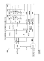
- FIG. 1 shows a semiconductor memory MEM in one embodiment.
- the semiconductor memory MEM is formed as a ferroelectric memory on a silicon substrate using a CMOS process.
- the ferroelectric memory is used as a work memory of a portable device such as a mobile phone or a digital camera, or a consumer device such as a video recorder, for example, a work memory such as an IC card or a wireless tag (RFID).
- the semiconductor memory MEM may operate in synchronization with the clock or may operate asynchronously with the clock.
- the semiconductor memory MEM may be designed as a memory macro (IP) mounted on a system LSI or the like, or may be designed as a semiconductor memory device enclosed in a package.
- IP memory macro
- the semiconductor memory MEM includes an address buffer ADB, command buffer CMDB, common word decoder CWDEC, word plate driver WPDRV, column decoder CDEC, operation control circuit CTRL, memory cell array ARY, column selector CSEL, sense amplifier SA, write amplifier WA and data input.
- An output circuit IOB is included.
- the address buffer ADB receives the address signal AD via the address terminal, and outputs the received signal to the common word decoder CWDEC and the column decoder CDEC as the row address signal RA and the column address signal CA.
- the address buffer ADB has a function of latching an address signal.
- the row address signal RA is an upper bit of the address signal AD and is supplied to select the word line WL.
- the column address signal CA is a lower bit of the address signal AD and is supplied to select the bit line BL.
- the row address signal RA and the column address signal CA are simultaneously supplied to different address terminals AD.
- the address buffer ADB may have a function of predecoding the address signal AD. At this time, the row address signal RA and the column address signal CA are predecode signals.
- the command buffer CMDB receives the command signal CMD for operating the memory array ARY and decodes the received command signal CMD.
- the command signal CMD is a chip enable signal / CE, a write enable signal / WE, and an output enable signal / OE.
- the command buffer CMDB outputs a read control signal RDZ when the command signal CMD indicates a read command.
- the command buffer CMDB outputs a write control signal WRZ when the command signal CMD indicates a write command.
- the command buffer CMDB outputs an address latch signal ALT in response to the chip enable signal / CE.
- the address latch signal ALT may be generated by the operation control circuit CTRL. Note that when the semiconductor memory MEM has a plurality of operation modes, the command buffer CMDB has a function of decoding the command signal CMD for changing the operation mode and outputting it as an operation mode change signal to the operation control circuit CTRL.
- the common word decoder CWDEC receives a row address signal RA, a column address signal CA, and a plate selection signal PLCLK.
- the common word decoder CWDEC outputs a row decode address signal RDA for selecting the word line WL while the plate selection signal PLCLK is at a low level.
- the common word decoder CWDEC outputs a row decode address signal RDA for selecting the plate line PL while the plate selection signal PLCLK is at a high level.
- the row decode address signal RDA is commonly used for selecting the word line WL and the plate line PL.
- the number of decode address signal lines for selecting the word line WL and the plate line PL can be reduced, and the wiring area of the signal lines can be reduced.
- An example of the common word decoder CWDEC is shown in FIG.
- the word plate driver WPDRV receives a row decode address signal RDA, a word latch signal WLTZ, a plate latch signal PLTZ, a word activation signal WACTZ, and a plate activation signal PACTZ.
- the word plate driver WPDRV latches the row decode address signal RDA for selecting the word line WL in synchronization with the word latch signal WLTZ.
- Word plate driver WPDRV latches row decode address signal RDA for selecting plate line PL in synchronization with plate latch signal PLTZ.
- the word plate driver WPDRV activates one of the word lines WL to a high level in synchronization with the word activation signal WACTZ when a valid row decode address signal RDA corresponding to the word line WL is latched.
- the word plate driver WPDRV activates one of the plate lines PL to a high level in synchronization with the plate activation signal PACTZ when a valid row decode address signal RDA corresponding to the plate line PL is latched.
- An example of the word plate driver WPDRV is shown in FIG.
- the column decoder CDEC decodes the column address signal CA and generates a column decode signal CDA according to the decoding result.
- the column decoder CDEC outputs a column decode signal CDA to the column selector CSEL.
- the operation control circuit CTRL receives the read control signal RDZ or the write control signal WRZ, and receives the common word decoder CWDEC, word plate driver WPDRV, column decoder CDEC, column selector CSEL, sense amplifier SA, write amplifier WA, data input / output circuit IOB, etc.
- a plurality of control signals for operating are sequentially generated and output.
- the control signals include a plate selection signal PLCLK, a word latch signal WLTZ, a plate latch signal PLTZ, a word activation signal WAACTZ, a plate activation signal PACTZ, a sense amplifier enable signal SAEN, a write amplifier enable signal WAEN, and a data input control signal DINZ. And a data output control signal DOUTZ.
- the control signal is a timing signal that determines the operation timing of the common word decoder CWDEC, the word plate driver WPDRV, the column decoder CDEC, the column selector CSEL, the sense amplifier SA, the write amplifier WA, the data input / output circuit IOB, and the like.
- the memory cell array ARY has a plurality of ferroelectric memory cells MC arranged in a matrix.
- the columns of memory cells MC arranged in the horizontal direction in the figure are connected to a common word line WL (WL0, WL1, etc.).
- the columns of memory cells MC arranged in the vertical direction in the figure are connected to a common bit line BL (BL00, BL01, etc.).
- a predetermined number of memory cells MC arranged in a rectangular region and arranged in the horizontal and vertical directions in the figure are connected to a common plate line PL (PL00, etc.).
- the memory cell array ARY shown in FIG. 1 shows a part of the memory block MB00 of FIG.
- the connection relationship between the memory cell MC and the plate line PL is shown in FIG.
- the memory cell MC has a selection transistor T1 (nMOS transistor) and a ferroelectric capacitor F1 arranged in series between the bit line BL and the plate line PL. That is, the memory cell MC is a so-called 1T1C type.
- the selection transistor T1 is turned on when the gate receives a high-level word line signal WL.
- the ferroelectric capacitor F1 operates as a variable capacitor by utilizing the fact that residual polarization remains even when the applied voltage is zero.
- the remanent polarization value of the ferroelectric capacitor F1 is changed by the write operation of the memory cell MC.
- the memory cell MC stores a logical value of data according to the remanent polarization value. That is, the semiconductor memory MEM operates as a rewritable nonvolatile memory.
- the memory cell MC may be a so-called 2T2C type.
- the 2T2C type memory cell MC has a pair of selection transistors (nMOS transistors) and a pair of ferroelectric capacitors. The gates of the select transistor pair are connected to a common word line WL. Ferroelectric capacitor pairs store data of opposite logic and are connected to complementary bit lines, respectively.
- the column selector CSEL has a plurality of column switches that connect the bit line BL to the sense amplifier SA and the write amplifier WA.
- a column switch corresponding to a valid column decode signal CDA is turned on in synchronization with a control signal output from the operation control circuit CTRL during a read operation and a write operation.
- the sense amplifier SA operates in synchronization with the sense amplifier enable signal SAEN during a read operation.
- the sense amplifier SA amplifies the difference between the voltage read on the bit line BL selected by the column switch during the read operation and the reference voltage VREF (FIG. 9), and uses the amplified signal as read data for the data input / output circuit. Output to IOB.
- the sense amplifier SA is shared by the plurality of bit lines BL via the column selector CSEL. Thereby, the number of sense amplifiers SA can be reduced.
- the sense amplifier SA may be disposed between the column selector CSEL and the memory cell array ARY. At this time, a sense amplifier is arranged for each bit line BL.
- the write amplifier WA operates in synchronization with the write amplifier enable signal WAEN during the write operation.
- the write amplifier WA outputs write data supplied via the data input / output circuit IOB during the write operation to the bit line BL selected by the column switch.
- the data input / output circuit IOB receives write data supplied to the data input / output terminal I / O in synchronization with the data input control signal DINZ, and outputs the received data to the write amplifier WA.
- the data input / output circuit IOB receives the read data from the memory cell MC via the sense amplifier SA, and outputs the received data to the data input / output terminal I / O in synchronization with the data output control circuit DOUTZ.
- the data input / output terminal I / O is, for example, 16 bits (I / O 0-15).
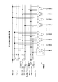
- FIG. 2 shows an example of the common word decoder CWDEC shown in FIG.
- the row address signal RA is 4 bits (RA0-3) and the column address signal CA is 2 bits (CA0-1) is shown.
- the common word decoder CWDEC generates 16 row decode signals RDA0-15.
- the row address signal RA is 8 bits and the column address signal CA is 6 bits.
- the common word decoder CWDEC generates 256 row decode signals RDA0-255.
- the common word decoder CWDEC has a selector SEL (SEL0-1) and a plurality of AND circuits.
- the selector SEL0 outputs the row address signal RA0 as the address signal A0 when the plate selection signal PLCLK is low, and outputs the column address signal CA0 as the address signal A0 when the plate selection signal PLCLK is high.
- the selector SEL1 outputs the row address signal RA1 as the address signal A1 when the plate selection signal PLCLK is low, and outputs the column address signal CA1 as the address signal A1 when the plate selection signal PLCLK is high. .
- the number of selectors SEL is determined according to the number of divisions of the columns (horizontal direction in FIG. 4) of the memory cell array ARY.
- the number of divided columns is equal to the number of memory blocks MB connected to one word line WL.
- the number of divided columns is equal to the number of word lines WL connected to one memory block MB.
- Memory block MB is connected to different plate lines PL.
- the number of divided columns and the number of word lines WL connected to one memory block MB are four.
- a selector SEL2 that receives the row address signal RA2 and the column address signal CA2 is arranged in addition to FIG.
- the number of word lines WL connected to one memory block MB is eight.
- the number of divided columns is two, only one selector SEL that receives row address signal RA0 and column address signal CA0 is arranged. At this time, the number of word lines WL connected to one memory block MB is two.
- the AND circuit decodes the 4-bit address signal A0 (or / A0), A1 (or / A1), A2 (or / A2), A3 (or / A3), and when all the received signals are at the high level
- the row decode address signal RDA (any one of RDA0-15) is set to a high level.
- the plurality of AND circuits operate as a decode circuit that decodes a 4-bit address signal A0-A3 (or / A0- / A3) and activates one of the row decode address signals RDA0-15.
- the common word decoder CWDEC sets one of the row decode address signals RDA0-15 to a high level according to the row address signal RA0-3 when the plate selection signal PLCLK is at a low level, and the remaining row decode address signal RDA. Is held at a low level. At this time, as will be described with reference to FIG. 3, one of the word lines WL is selected. When the plate selection signal PLCLK is at a high level, the common word decoder CWDEC sets one of the row decode address signals RDA0-15 to a high level according to the column address signal CA0-1 and the row address signal RA2-3, and the rest The row decode address signal RDA is held at a low level. At this time, one of the plate lines PL is selected as described in FIG.
- the AND circuit responds to the selectors SEL0-1 to generate the row decode address signal RDA0-15 for selecting the word line WL and the row decode address signal for selecting the plate line PL. It operates as an address decoding circuit that generates RDA0-15.
- the word decoder for selecting the word line WL and the plate decoder for selecting the plate line PL can be replaced with the common word decoder CWDEC.
- the circuit scale of the plate decoder in this example, the common word decoder CWDEC
- the circuit scale of the plate decoder can be reduced.
- the circuit scale of the plate decoder can be reduced.
- the circuit scale of the plate decoder can be reduced.
- the circuit scale of the plate decoder can be reduced.
- the circuit scale of the plate decoder can be reduced.
- the common word decoder CWDEC directly decodes the row address signal RA0-3 and the column address signal CA0-1 supplied to the external address terminal AD to generate a row decode address signal RDA.
- the row decode address signal RDA is generated without using the previous signal from the decode circuit (AND circuit). Therefore, the number of circuits (transistors) required for generating the row decode address signal RDA can be reduced. Therefore, the row decode address signal RDA can be generated quickly, and the access time (read operation time and write operation time) of the semiconductor memory MEM can be shortened.
- the AND circuit receives the low level address signals A0-A3 and / A0- / A3 during the standby period when the read operation or the write operation is not executed, and holds all the row decode address signals RDA0-15 at the low level. .
- the address signals A0-A3, / A0- / A3 are supplied to the AND circuit via the enable circuit.
- the enable circuit is an AND circuit that receives one of address signals A0-A3 and / A0- / A3 and an enable signal.
- the enable signal is set to a high level during an access operation (a read operation or a write operation), and is set to a low level during a standby period. In the standby period, all the enable circuits output a low level to the AND circuit, so that all the row decode address signals RDA0-15 are held at a low level.
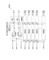
- FIG. 3 shows an example of the word plate driver WPDRV shown in FIG.
- the word plate driver WPDRV is a driver circuit, and has a plurality of sub word plate drivers SWPDRV that drive a pair of the word line WL and the plate line PL. Since the sub word plate driver SWPDRV is the same circuit, only the sub word plate driver SWPDRV that drives the word line WL15 and the plate line PL33 will be described.
- the sub word plate driver SWPDRV has switch circuits WSW and PSW, latch circuits WLT and PLT, and two AND circuits.
- the switch circuit WSW supplies the row decode address signal RDA15 to the latch circuit WLT while the word latch signal WLTZ is at a high level.
- the switch circuit PSW supplies the row decode address signal RDA15 to the latch circuit PLT while the plate latch signal PLTZ is at a high level.
- Each latch circuit WLT, PLT has, for example, a pair of inverters whose inputs and outputs are connected to each other in order to hold the logic level of the row decode address signal RDA15.
- the AND circuit connected to the word line WL15 drives the word line WL15 in synchronization with the word activation signal WACTZ and activates the word line WL15 to the high level.
- the AND circuit connected to the plate line PL33 drives the plate line PL33 in synchronization with the plate activation signal PACTZ and activates the plate line PL33 to the high level.
- the word plate driver WPDRV outputs a high level of any one of the row decode address signals RDA0-15 for selecting the word line WL and a row decode address signal RDA0 for selecting the plate line PL during the read operation and the write operation. Sequentially receive any high level of -15. Any one of the latch circuits WLT latches the high-level row decode address signal RDA and outputs a high level. The other latch circuit WLT outputs a low level. Any one of the latch circuits PLT latches the high-level row decode address signal RDA and outputs a high level. The other latch circuit PLT outputs a low level. Then, the word plate driver WPDRV sequentially drives any one of the word lines WL0-15 and any one of the plate lines PL00-03, PL10-13, PL20-23, PL30-33 to a high level.
- the row decode address signals RDA0-15 sequentially supplied to the word plate driver WPDRV are selectively latched in one of the latch circuits WLT, PLT using the switch circuits WSW, PSW.
- the word line WL and the plate are transmitted according to the row decode address signal RDA0-15 for the word line WL and the row decode address signal RDA0-15 for the plate line PL transmitted to the common signal line RDA0-15, respectively.
- the line PL can be activated reliably.
- the logic level of the row decode address signal RDA0-15 latched by the latch circuit WLT is output as the word line signal WL in synchronization with the word activation signal WAACTZ.
- the logic level of the row decode address signal RDA0-15 latched by the latch circuit PLT is output as the plate line signal PL in synchronization with the plate activation signal PACTZ. Therefore, even if the row decode address signal RDA0-15 for the word line WL and the row decode address signal RDA0-15 for the plate line PL are supplied to the common signal lines RDA0-15 in a time division manner, at a desired timing.
- the word line WL and the plate line PL can be activated. In other words, as shown in FIG. 9, the word line WL and the plate line PL can be activated overlapping each other.
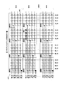
- FIG. 4 shows an example of the memory cell array ARY shown in FIG.
- the memory cell array ARY has 16 memory blocks MB (MB00-03, MB10-13, MB20-23, MB30-33) arranged in a matrix.
- a memory group MG (MG0-3) is configured by four memory blocks MB arranged in the horizontal direction in the figure.
- the number assigned to the memory group MG is indicated by the row address signal RA3-2.
- the memory block MB is connected to different plate lines PL (PL00-03, PL10-13, PL20-23, PL30-33). That is, the number of memory blocks MB is equal to the number of plate lines PL.
- the upper bits of the two-digit numbers assigned to the memory block MB and the plate line PL have the same value as the numbers assigned to the memory group MG, and are indicated by the row address signal RA3-2.
- the lower bits of the 2-digit number are indicated by the column address signal CA1-0.
- Each memory block MB is connected to four word lines WL.
- Four memory blocks MB in each memory group MG are connected to four common word lines WL.
- the word lines WL and the plate lines PL indicated by thick solid lines are wired alternately. That is, four plate lines PL (for example, PL00-03) are wired on the four memory blocks MB in each memory group MG.
- Each plate line PL branches to a plate line indicated by a thick broken line in the same number of memory blocks MB and is connected to the memory cell MC. That is, one of the four plate lines PL (for example, PL00-03) is connected to each memory block MB. Black square marks in the figure indicate contacts for branching the plate line PL.
- the word line WL and the plate line PL are selected using a common row address signal RA2-3.
- a plurality of memory groups MG can be formed only by increasing AND circuits, and the number of divisions of the plate line PL can be increased. That is, each of the plate lines PL divided into a large number can be selected by a simple decoding circuit.
- the semiconductor memory MEM having a large number of divisions of the plate line PL the scale of the logic circuit for selecting the plate line PL can be reduced, and the chip size of the semiconductor memory MEM can be reduced.
- Each memory block MB is connected to four bit lines BL0-3 (BL00-03, BL10-13, BL20-23, BL30-33).
- the four memory blocks MB arranged in the vertical direction in the figure are connected to four common bit lines BL0-3 (for example, BL00-03).
- the upper bit of the two-digit number attached to the bit line BL is indicated by a column address signal CA.
- the lower bits of the two-digit number indicate the number of the data terminal I / O.
- the column selector CSEL shown in FIG. 1 selects one of the four bit line groups BL00-03, BL10-13, BL20-23, BL30-33 as the lower bit of the column address signal CA. Depending on the value, it is connected to a sense amplifier SA or a write amplifier WA.
- each bit line group has four bit lines.
- each bit line group has 16 bit lines BL corresponding to the data terminals I / O0-15.
- the data terminal I / O is 1 bit (I / O0)
- each bit line group has only one bit line.
- Each memory block MB has 16 memory cells MC arranged in a matrix.
- a row address signal RA3-0 in binary number “1011” and a column address signal CA1-0 in binary number “10” are supplied in a read operation or a write operation.
- the word line WL11 indicated by the row address signal RA3-0 and the plate line PL22 indicated by the row address signal RA3-2 and the column address signal CA1-0 are selected.
- data is read from the memory cells MC indicated by thick circles in the memory block MB22 to the bit lines BL20-23.
- data is written to the memory cells MC indicated by thick circles in the memory block MB22 via the bit lines BL20-23.
- the common word decoder CWDEC shown in FIG. 2 has three selectors SEL0-2, as described above, eight memory blocks MB are formed along the word line WL (the horizontal direction in the figure). . That is, eight memory groups MG are formed. Eight memory blocks MB of each memory group MG are connected to eight common word lines WL. Selectors SEL0-2 receive row address signal RA0-2 or column address signal CA0-2 according to plate selection signal PLCLK. In the read operation or the write operation, one of the eight memory blocks MB in the memory group MG is selected according to the column dress signal CA0-2. On the eight memory blocks MB in the memory group MG, eight plate lines PL are wired and connected to one of the eight memory blocks MB.
- the memory cell array ARY has 256 word lines WL. Since eight word lines WL are connected to each memory block MB, eight memory blocks MB are arranged in the vertical direction in the figure. That is, the number of memory groups MG is eight. The total number of memory blocks MB is 256 (8 horizontal and 8 vertical), which is equal to the number of plate lines PL and word lines WL.
- the number of selectors SEL is m
- 2 m memory blocks MB are arranged along the word line WL (in the horizontal direction in the figure).
- the plate line PL is wired for each memory block MB.
- Each memory group MG and each memory block MB are connected to 2 m word lines WL.
- the number of bits of the row address signal RA is n
- the number of word lines WL, the number of plate lines PL, and the number of memory blocks MB are all 2 to the nth power.
- the number of memory groups MG is 2 to the (n ⁇ m) power.
- FIG. 5 shows an example of the wiring layout of the memory cell array ARY shown in FIG.
- the memory group MG3 memory blocks MB30-33) shown in FIG. 4 is shown.
- the plate line PL31 is shaded for easy understanding of the wiring of the plate line.
- the polysilicon layer Poly is a wiring layer for forming the gate of the transistor.
- the first, second, third, fourth, and fifth metal wiring layers are layers above the polysilicon layer Poly, and the larger the number, the farther from the semiconductor substrate.
- the word line WL is wired using the polysilicon layer Poly and the third metal wiring layer M3.
- the polysilicon layer Poly is a wiring layer for forming the gate of the transistor.
- the word line WL formed of the polysilicon wiring Poly is connected to the word line WL formed of the third metal wiring M3 through a contact indicated by a black square mark.
- the plate line PL is wired using the first metal wiring layer M1, the fourth metal wiring layer M4, and the fifth metal wiring layer M5.
- the plate line formed by the fifth metal wiring M5 is wired in the horizontal direction in the figure, and is connected to the plate line PL formed by the fourth metal wiring M4 through a contact.
- the plate line PL formed of the fourth metal wiring M4 is connected to the plate line PL formed of the first metal wiring M1 through a contact.
- Each memory cell MC is connected to a word line WL formed of a polysilicon wiring Poly and a plate line PL formed of a first metal wiring M1.
- the memory cell MC is manufactured by, for example, a stack type manufacturing process.
- the bit line BL is formed using the second metal wiring layer on the memory cells MC arranged in the vertical direction in the drawing.
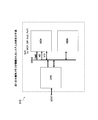
- FIG. 6 shows an example of a system SYS on which the semiconductor memory MEM shown in FIG. 1 is mounted.
- the system SYS (user system) constitutes at least a part of a microcomputer system such as a portable device.
- the semiconductor memory MEM is mounted on the same system SYS as in FIG.
- the system SYS has a system-on-chip SoC in which a plurality of macros are integrated on a silicon substrate.
- the system SYS has a multi-chip package MCP in which a plurality of chips are stacked on a package substrate.
- the system SYS has a system-in-package SiP in which a plurality of chips are mounted on a package substrate such as a lead frame.
- the system SYS may be configured in the form of chip-on-chip CoC or package-on-package PoP.
- the SoC has a CPU (controller), the semiconductor memory MEM and the peripheral circuit PERI shown in FIG.
- the CPU, the semiconductor memory MEM, and the peripheral circuit PERI are connected to each other by a system bus SBUS.
- the CPU accesses the semiconductor memory MEM and the peripheral circuit PERI and controls the operation of the entire system.
- the semiconductor memory MEM performs a read operation and a write operation in response to an access command CMD (access request) from the CPU and an address signal AD.
- the SoC is connected to an upper system via the external bus SCNT.
- the minimum configuration of the system SYS is a CPU and a semiconductor memory MEM.
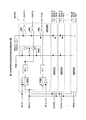
- FIG. 7 shows an example of the read operation of the semiconductor memory MEM shown in FIG.
- the semiconductor memory MEM executes a read operation when it receives a read command (a low level L chip enable signal / CE, a high level H write enable signal / WE, and a low level L output enable signal / OE) ( FIG. 7 (a)).
- the CPU shown in FIG. 6 outputs an address signal AD together with the read command to the semiconductor memory MEM (FIG. 7B).
- the command buffer CMDB shown in FIG. 1 activates the read control signal RDZ and the address latch signal ALTZ to a high level in response to the read command (FIG. 7 (c, d)).
- the write control signal WRZ is held at the low level L (FIG. 7 (e)).
- the address buffer ADB latches the address signal AD in synchronization with the address latch signal ALTZ, and outputs the latched address signal AD as the row address signal RA and the column address signal CA (FIG. 7 (f)).
- the selector SEL0-1 of the common word decoder CWDEC shown in FIG. 2 outputs the row address signal RA0-1 as the address signals A0-1 and / A0-1 while the plate selection signal PLCLK is at a low level (FIG. 7 ( g)).
- the common word decoder CWDEC sets a row decode address signal RDA (for example, RDAa: a is 0 to 15) for selecting the word line WL to a high level based on the row address signal RA0-3 (FIG. 7 (h)). Other row decode address signals RDA are held at a low level.
- the word plate driver WPDRV latches the row decode address signal RDAa in synchronization with the word latch signal WLTZ (FIG. 7 (i)
- the selector SEL0-1 of the common word decoder CWDEC receives the high level plate selection signal PLCLK and outputs the column address signal CA0-1 as the address signals A0-1 and / A0-1 (FIG. 7 (j)). ).
- the operation control circuit CTRL changes the plate selection signal PLCLK from the low level to the high level after a predetermined time (for example, 10 ns) after receiving the read command or the write command.
- the common word decoder CWDEC receives a row decode address signal RDA (for example, RDAb: b is any of 0-15) for selecting the plate line PL based on the column address signal CA0-1 and the row address signal RA2-3.
- the high level is set (FIG. 7 (k)).
- Other row decode address signals RDA are held at a low level.
- the word plate driver WPDRV latches the row decode address signal RDAb in synchronization with the plate latch signal PLTZ (FIG. 7 (l)).
- the word plate driver WPDRV activates the word line WLa corresponding to the row decode address signal RDAa to a high level in synchronization with the word activation signal WACTZ (FIG. 7 (m)). Other word lines WL are held at a low level. By activation of the word line WLa, the ferroelectric capacitor F1 of the memory cell MC is connected to the bit line BL. Next, the word plate driver WPDRV activates the plate line PLb corresponding to the row decode address signal RDAb to a high level in synchronization with the plate activation signal PACTZ (FIG. 7 (n)). The other plate lines PL are held at a low level. The activation period of the plate line PLb is included in the activation period of the word line WLa.
- a charge (voltage) corresponding to the residual polarization of the ferroelectric capacitor F1 is read out to the bit line BL (FIG. 7 (o)).
- a solid line shows a waveform when logic 1 is read from the memory cell MC to the bit line BL.
- a broken line shows a waveform when logic 0 is read from the memory cell MC to the bit line BL.
- a reference charge (voltage) is read from the reference memory cell.
- the column selector CSEL connects the bit line BL corresponding to the column address signal CA to the sense amplifier SA.
- the sense amplifier SA differentially amplifies the difference between the voltage of the bit line BL and the reference voltage, and determines the logic of the data held in the memory cell MC (FIG. 7 (p)).
- the data input / output circuit IOB outputs the read data amplified by the sense amplifier SA to the data terminal I / O (FIG. 7 (q)).
- the sense amplifier SA is deactivated and the bit line BL is set to a low level (FIG. 7 (r)).
- the word activation signal WACTZ and the word line WLa are deactivated to a low level, and the read operation is completed (FIG. 7 (s)).
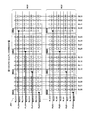
- FIG. 8 shows an example of the write operation of the semiconductor memory MEM shown in FIG. Detailed descriptions of the same operations as those in FIG. 7 are omitted.
- the semiconductor memory MEM executes a write operation when it receives a write command (a low level L chip enable signal / CE, a low level L write enable signal / WE, and a high level H output enable signal / OE) ( FIG. 8 (a)).
- the CPU shown in FIG. 6 outputs the address signal AD and the data signal I / O (write data) together with the write command to the semiconductor memory MEM (FIG. 8 (b, c)).
- the command buffer CMDB activates the write control signal WRZ and the address latch signal ALTZ to a high level in response to the write command (FIG. 8 (d, e)).
- the read control signal RDZ is held at a low level (FIG. 8 (f)).
- the waveforms from the address latch signal ALTZ to the plate activation signal PACTZ and the plate line PLb are the same as those in FIG.
- a charge (voltage) corresponding to the residual polarization of the ferroelectric capacitor F1 is read out to the bit line BL (FIG. 8 (g)).
- the column selector CSEL connects the bit line BL corresponding to the column address signal CA to the write amplifier WA.
- the write amplifier WA outputs a level corresponding to the logic of the write data to the bit line BL.
- the plate line PL is deactivated to a low level before the voltage of the bit line BL is changed by the write data from the write amplifier WA (FIG. 8 (h)). Then, according to the low level of the plate line PL and the voltage level of the bit line BL, logic 1 or logic 0 is written into the memory cell MC (FIG. 8 (i)). Thereafter, the bit line BL is set to a low level by the write amplifier WA (FIG. 8 (j)). Next, the word activation signal WACTZ and the word line WLa are deactivated to a low level, and the write operation is completed (FIG. 8 (k)).
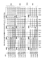
- FIG. 9 shows an example of the operation of the memory cell array ARY of the semiconductor memory MEM shown in FIG.
- FIG. 9 shows a period in which the word line WL and the plate line PL are activated to a high level in FIGS. 7 and 8.
- the voltage rise of the bit line BL when the plate line PL is driven to a high level is slight. Therefore, regardless of the logic of the data read from the memory cell MC, the bit line BL is at a low level with respect to the high level plate line PL (FIG. 9A).
- This state indicates writing of logic 0 to the memory cell MC. That is, when logic 1 is read from the memory cell MC to the bit line BL, the remanent polarization value of the ferroelectric capacitor F1 is inverted, and the data held in the memory cell MC is rewritten to logic 0.
- the sense amplifier SA is activated by the sense amplifier enable signal SAEN before the plate line PL changes to a low level (FIG. 9B).
- the sense amplifier SA differentially amplifies the voltage of the bit line (for example, power supply voltage) BL and the reference voltage Vref, and raises the voltage of the bit line BL to a high level ( FIG. 9 (c)). Then, when the bit line BL becomes a high level with respect to the low level plate line PL, the logic 1 is rewritten to the memory cell MC.
- writing of logic 0 to the memory cell MC occurs during the high level period of the plate line PL (FIG. 9D). That is, the memory cell MC that holds logic 1 is rewritten to logic 0.
- the write amplifier WA is activated after the plate line PL is changed to a low level by the write amplifier enable signal WAEN (FIG. 9E).
- WAEN write amplifier enable signal
- both the plate line PL and the bit line BL are set to a low level, and the remanent polarization value of the ferroelectric capacitor F1 does not change. That is, the memory cell MC maintains the logic 0 rewritten by the activation of the plate line PL (FIG. 9 (f)).
- the plate line PL is set to a low level, and the bit line BL is set to a high level (for example, a power supply voltage).
- the memory cell MC is rewritten to logic 1 (FIG. 9 (g)). Then, the write operation of logic 0 and logic 1 to the memory cell MC is completed.
- the high level voltage of the word line WL may be set higher than the power supply voltage during the period in which the sense amplifier SA or the write amplifier WA operates. At this time, the high voltage is preferably equal to or higher than the value obtained by adding the threshold voltage of the selection transistor T1 to the power supply voltage.
- the word decoder for selecting the word line WL and the plate decoder for selecting the plate line PL can be replaced with the common word decoder CWDEC.
- the circuit scale of the plate decoder in this example, the common word decoder CWDEC
- the circuit scale of the plate decoder can be reduced.
- the row decode address signal RDA is commonly used for selecting the word line WL and the plate line PL.
- FIG. 10 shows an example of the common word decoder CWDEC in the semiconductor memory MEM of another embodiment.
- the semiconductor memory MEM is a ferroelectric memory.
- the common word decoder CWDEC is different from that in FIG. 2, and the memory cell array ARY shown in FIGS. 11 and 12 is different from those in FIGS.
- Other configurations are the same as those in FIGS. 1 and 3.
- the semiconductor memory MEM is used as, for example, a work memory such as an IC card or a wireless tag (RFID), a work memory of a portable device such as a mobile phone or a digital camera, or a work memory of a consumer device such as a video recorder.
- the semiconductor memory MEM may operate in synchronization with the clock or may operate asynchronously with the clock.
- the semiconductor memory MEM is mounted on, for example, the system SYS shown in FIG.
- the common word decoder CWDEC receives a signal obtained by inverting the logic of the column address signal CA1-0 by the selector SEL0-1.
- Other configurations of the common word decoder CWDEC are the same as those in FIG. For example, when the column address signal CA1-0 is “00”, the common word decoder CWDEC sets any one of the row decode address signals RDA3, RDA7, RDA11, and RDA15 to a high level according to the row address signal RA3-2. . When the column address signal CA1-0 is “01”, the common word decoder CWDEC sets any one of the row decode address signals RDA2, RDA6, RDA10, and RDA14 to a high level according to the row address signal RA3-2.
- FIG. 11 shows an example of the memory cell array ARY in the semiconductor memory MEM having the common word decoder CWDEC shown in FIG. Detailed description of the same configuration as in FIG. 4 is omitted.
- the layout of the memory group MG, memory block MB, word line WL, and bit line BL is the same as in FIG. Since the relationships among the plate lines PL33-30, PL23-20, PL13-10, and PL03-00 are the same, the plate line PL33-30 will be described below.
- the logic of the column address signal CA1-0 supplied to the common word decoder CWDEC is inverted. Therefore, for example, the plate line PL33 is selected when the column address signal CA1-0 is “00”. The plate line PL32 is selected when the column address signal CA1-0 is “01”. The plate line PL31 is selected when the column address signal CA1-0 is “10”. The plate line PL30 is selected when the column address signal CA1-0 is “11”. For this reason, the plate lines PL33, PL32, PL31, and PL30 are also indicated as symbols PL30b, PL31b, PL32b, and PL33b.
- the numerical values 0b, 1b, 2b, and 3b of the code indicate the value (decimal number) of the column address signal CA1-0.
- the symbols 0b, 1b, 2b, and 3b "b" indicate logic inversion ("/"; bar).
- Each plate line PL33-30 is connected to a memory block MB having the same value as the numeral PL30b-33b. For this reason, the position of the contact (black square mark) for branching the plate line PL is different from FIG.
- FIG. 12 shows an example of the wiring layout of the memory cell array ARY shown in FIG. Detailed description of the same configuration as in FIG. 5 is omitted.
- the memory group MG3 memory blocks MB30-33
- the plate line PL finth metal wiring layer M5 wired in the horizontal direction in the drawing from the left end of the memory cell array ARY to the memory block MB is shown by shading.
- control signal lines such as a plate activation signal line PACTZ are wired from the operation control circuit CTRL arranged at the lower right of the memory cell array ARY to the sub word plate driver SWPDRV toward the upper side of FIG.
- the upper sub-word plate driver SWPDRV in FIG. 3 receives the plate activation signal PACTZ later than the lower sub-word plate driver SWPDRV in FIG. Therefore, in the read operation and the write operation, the plate line PL33 is activated relatively late, and the plate line PL30 is activated relatively early.
- the plate line PL33 corresponding to the sub-word plate driver SWPDRV to which the plate activation signal PACTZ is transmitted slowly has a short horizontal length shown in FIG. 12 and a small load capacity.
- the plate line PL30 corresponding to the sub-word plate driver SWPDRV to which the plate activation signal PACTZ is transmitted early is long in the horizontal direction indicated by shading and has a large load capacity. Therefore, the timings at which the high level pulses generated on the plate lines PL30-33 are transmitted to the memory cells MC can be aligned with each other. In other words, the activation timings of the plate line signals PL30-33 can be aligned with each other.
- the same effect as that of the above-described embodiment can be obtained. Furthermore, since the activation period of the plate line signal PL can be made uniform, the operation margin of the semiconductor memory MEM can be improved.
- FIG. 13 shows an example of a semiconductor memory MEM in another embodiment.
- the semiconductor memory MEM is a ferroelectric memory.
- the semiconductor memory MEM is used as, for example, a work memory such as an IC card or a wireless tag (RFID), a work memory of a portable device such as a mobile phone or a digital camera, or a work memory of a consumer device such as a video recorder.
- the semiconductor memory MEM may operate in synchronization with the clock or may operate asynchronously with the clock.
- the semiconductor memory MEM is mounted on, for example, the system SYS shown in FIG.
- the semiconductor memory MEM is different from FIG. 1 in the word plate driver WPDRV and the memory cell array ARY.
- the semiconductor memory MEM receives a row address signal RA that is one bit larger than that in FIG. Other configurations are the same as those in FIG.
- the memory cell array ARY shown in FIG. 13 shows a part of the memory block MB00 of FIG.
- each plate line PL is wired in common to the two word lines WLE and WLO.
- the word plate driver WPDRV selects one of the word lines WLE and WLO according to the logic of the most significant bit of the row address signal RA. Note that the word lines WLE and WLO may be selected using the least significant bit of the row address signal RA.
- FIG. 14 shows an example of the word plate driver WPDRV shown in FIG. Detailed description of the same configuration as in FIG. 3 is omitted.
- the word plate driver WPDRV has a plurality of sub word plate drivers SWPDRV for driving a pair of word lines WLE and WLO and one plate line PL. Since the sub word plate driver SWPDRV is the same circuit, only the sub word plate driver SWPDRV for driving the word lines WLE15, WLO15 and the plate line PL33 will be described.
- the sub word plate driver SWPDRV has a word selector WSEL and an AND circuit added to the sub word plate driver SWPDRV shown in FIG.
- the word selector WSEL has a CMOS transmission gate that is turned on or off according to the logic of the row address signal RA4.
- the word selector WSEL connects the output of the latch WLT to an AND circuit connected to the word line WLE15 when the row address signal RA4 is at a low level.
- the word selector WSEL connects the output of the latch WLT to an AND circuit connected to the word line WLO15 when the row address signal RA4 is at a high level.
- the AND circuit connected to the word lines WLE15 and WLO15 operates in synchronization with the word activation signal WACTZ.
- the row address signal RA is 9 bits (RA0-8), and the column address signal CA is 6 bits.
- the row address signal RA0-7 is supplied to the common word decoder CWDEC, and the row address signal RA8 is supplied to the word selector WSEL.
- FIG. 15 shows an example of the memory cell array ARY shown in FIG. Detailed description of the same configuration as in FIG. 4 is omitted.
- the memory cell array ARY has 16 memory blocks MB (MB00-03, MB10-13, MB20-23, MB30-33) arranged in a matrix as in FIG.
- each memory group MG and each memory block MB are connected to four word line pairs WLE and WLO.
- Each memory block MB has 32 memory cells MC.
- Other configurations are the same as those in FIG.
- each bit line group BL00-03, BL10-13, BL20-23, and BL30-33 has an example having four bit lines.
- each bit line group has 16 bit lines BL corresponding to the data terminals I / O0-15.
- the data terminal I / O is 1 bit (I / O0)
- each bit line group has only one bit line.
- each memory group MG has eight memory blocks MB as described above.
- Column selector SEL receives row address signal RA0-2 or column address signal CA0-2 in response to plate selection signal PLCLK. In the read operation or the write operation, one of the eight memory blocks MB in one memory group MG is selected according to the column dress signal CA0-2.
- Each memory block MB is connected to 16 word lines WL (eight word line pairs WLE, WLO).
- eight plate lines PL are wired and connected to one of the eight memory blocks MB.
- the row address signal RA is 9 bits (RA0-8)
- the memory cell array ARY has 512 word lines WL (256 word line pairs WLE, WLO). Since 16 word lines WL are connected to each memory block MB, eight memory blocks MB are arranged in the vertical direction in the figure. That is, the number of memory groups MG is eight.
- the total number of memory blocks MB is 256 (8 horizontal and 8 vertical), which is equal to the number of plate lines PL and word line pairs (WLE, WLO).
- each plate line PL when each plate line PL is wired in common to two word lines WLE and WLO, 2 m powers (m is a selector SEL) along the word line WL (horizontal direction in the figure).
- Number of memory blocks MB are arranged.
- the plate line PL is wired for each memory block MB.
- Each memory group MG and each memory block MB are connected to 2 m word line pairs (WLE, WLO).
- the number of word line pairs (WLE, WLO), the number of plate lines PL, and the number of memory blocks MB are both (n -1) Power.
- the number of memory groups MG is 2 to the (n-1-m) power.
- the same effect as that of the above-described embodiment can be obtained.
- the circuit scale of the common word decoder CWDEC can be reduced also in the semiconductor memory MEM in which each plate line PL is wired in common to the pair of word lines WLE and WLO.
- the number of row decode address signal lines RDA can be reduced, and the wiring area of the signal lines can be reduced. As a result, the chip size of the semiconductor memory MEM can be reduced.
- a signal obtained by inverting the logic of the column address signal CA0-1 may be supplied to the common word decoder CWDEC shown in FIG. 13 as shown in FIG.
- the memory cell array ARY (FIG. 15) is changed similarly to FIG. That is, plate line PL33 is connected to memory block MB30, and plate line PL32 is connected to memory block MB31. Plate line PL31 is connected to memory block MB32, and plate line PL30 is connected to memory block MB33.
Landscapes
- Engineering & Computer Science (AREA)
- Microelectronics & Electronic Packaging (AREA)
- Computer Hardware Design (AREA)
- Dram (AREA)
- Semiconductor Memories (AREA)
Abstract
Description
Claims (13)
- 複数のメモリセルと、
前記メモリセルに接続された複数のワード線と、
前記メモリセルに接続された複数のプレート線と、
前記ワード線を選択するための第1アドレス信号を第1期間に選択し、前記プレート線を選択するための第2アドレス信号を第2期間に選択するセレクタと、
前記セレクタにより選択された前記第1および第2アドレス信号を順次にデコードして、デコードアドレス信号のいずれかを順次に活性化するデコード回路と、
前記第1アドレス信号により活性化されたデコードアドレス信号に応じてワード線を駆動し、前記第2アドレス信号により活性化されたデコードアドレス信号に応じてプレート線を駆動するドライバ回路と
を備えていることを特徴とする半導体メモリ。 - 請求項1記載の半導体メモリにおいて、
前記デコード回路は、前記第1および第2アドレス信号とともに、前記ワード線と前記プレート線に共通に第3アドレス信号をデコードして前記デコードアドレス信号のいずれかを順次に活性化し、
前記ドライバ回路は、前記第1および第3アドレス信号により活性化されたデコードアドレス信号に応じてワード線を駆動し、前記第2および第3アドレス信号により活性化されたデコードアドレス信号に応じてプレート線を駆動すること
を特徴とする半導体メモリ。 - 請求項2記載の半導体メモリにおいて、
前記第3アドレス信号により識別される複数のメモリグループと、
前記各メモリグループに設けられ、前記第2アドレス信号により識別され、前記メモリセルを有する複数のメモリブロックと
を備え、
前記プレート線は、前記メモリブロック毎に配線され、
前記第1アドレス信号で識別される複数の前記ワード線は、前記メモリグループ毎に、前記メモリグループ内のメモリブロックに共通に配線されていること
を特徴とする半導体メモリ。 - 請求項3記載の半導体メモリにおいて、
前記ワード線の数は、前記メモリブロックの数に等しいことを特徴とする半導体メモリ。 - 請求項2記載の半導体メモリにおいて、
前記メモリセルに接続された複数のビット線を備え、
前記第1および第3アドレス信号は、ワード線を選択するためのロウアドレスであり、
前記第2アドレス信号は、前記ビット線を選択するためのコラムアドレスであること
を特徴とする半導体メモリ。 - 請求項2ないし請求項5のいずれか1項記載の半導体メモリにおいて、
前記ドライバ回路は、前記デコードアドレス信号をそれぞれ受け、前記ワード線の1つおよび前記プレート線の1つに接続された複数のサブドライバ回路を備え、
前記各サブドライバ回路は、
対応するデコードアドレス信号のレベルを第1タイミング信号に同期してラッチする第1ラッチ回路と、
対応するデコードアドレス信号の活性化レベルを前記第1ラッチ回路がラッチしているときに、第2タイミング信号に同期して前記ワード線を活性化する第1活性化回路と、
対応するデコードアドレス信号のレベルを第3タイミング信号に同期してラッチする第2ラッチ回路と、
対応するデコードアドレス信号の活性化レベルを前記第2ラッチ回路がラッチしているときに、第4タイミング信号に同期して前記プレート線を活性化する第2活性化回路と
を備えていることを特徴とする半導体メモリ。 - 請求項6記載の半導体メモリにおいて、
読み出しコマンドまたは書き込みコマンドを受けてから所定時間後に、選択信号を第1レベルから第2レベルに変化し、前記選択信号が前記第1レベルの間に前記第1タイミング信号を生成し、前記第2レベルの間に前記第2、第3および第4タイミング信号を生成する動作制御回路を備え、
前記セレクタは、前記選択信号が前記第1レベルの間、前記第1アドレス信号を選択し、前記選択信号が前記第2レベルの間、前記第2アドレス信号を選択すること
を特徴とする半導体メモリ。 - 請求項1記載の半導体メモリにおいて、
読み出しコマンドまたは書き込みコマンドを受けてから所定時間後に、選択信号を第1レベルから第2レベルに変化する動作制御回路を備え、
前記セレクタは、前記選択信号が前記第1レベルの間、前記第1アドレス信号を選択し、前記選択信号が前記第2レベルの間、前記第2アドレス信号を選択すること
を特徴とする半導体メモリ。 - 請求項1記載の半導体メモリにおいて、
前記デコード回路は、前記第1および第2アドレス信号とともに、前記ワード線と前記プレート線に共通に第3アドレス信号をデコードして前記デコードアドレス信号のいずれかを活性化し、
前記ドライバ回路は、前記第1および第3アドレス信号により活性化されたデコードアドレス信号に応じて選択される一対の前記ワード線の1つを第4アドレス信号に応じて駆動し、前記第2および第3アドレス信号により活性化されたデコードアドレス信号に応じてプレート線を駆動すること
を特徴とする半導体メモリ。 - 請求項9記載の半導体メモリにおいて、
前記ドライバ回路は、前記デコードアドレス信号をそれぞれ受け、前記ワード線の2つおよび前記プレート線の1つに接続された複数のサブドライバ回路を備え、
前記各サブドライバ回路は、
対応するデコードアドレス信号のレベルを第1タイミング信号に同期してラッチする第1ラッチ回路と、
前記ワード線の2つにそれぞれ接続された一対の第1活性化回路と、
前記第1ラッチ回路の出力を前記第4アドレス信号に応じて前記第1活性化回路の一方に接続するワードセレクタと、
対応するデコードアドレス信号のレベルを第3タイミング信号に同期してラッチする第2ラッチ回路と、
対応するデコードアドレス信号の活性化レベルを前記第2ラッチ回路がラッチしているときに、第4タイミング信号に同期して前記プレート線を活性化する第2活性化回路と
を備え、
前記各第1活性化回路は、対応するデコードアドレス信号の活性化レベルをラッチしている前記第1ラッチ回路からの出力を、前記ワードセレクタを介して受けているときに、第2タイミング信号に同期して対応するワード線を活性化する
ことを特徴とする半導体メモリ。 - 複数のメモリセルと、前記メモリセルに接続された複数のワード線と、前記メモリセルに接続された複数のプレート線とを備えた半導体メモリの動作方法であって、
前記ワード線を選択するための第1アドレス信号を第1期間に選択し、
前記プレート線を選択するための第2アドレス信号を第2期間に選択し、
選択された前記第1および第2アドレス信号を順次にデコードして、デコードアドレス信号のいずれかを順次に活性化し、
前記第1アドレス信号により活性化されたデコードアドレス信号に応じてワード線を駆動し、
前記第2アドレス信号により活性化されたデコードアドレス信号に応じてプレート線を駆動する
ことを特徴とする半導体メモリの動作方法。 - 請求項11記載の半導体メモリの動作方法において、
前記第1および第2アドレス信号とともに、前記ワード線と前記プレート線に共通に第3アドレス信号をデコードして前記デコードアドレス信号のいずれかを順次に活性化し、
前記第1および第3アドレス信号により活性化されたデコードアドレス信号に応じてワード線を駆動し、
前記第2および第3アドレス信号により活性化されたデコードアドレス信号に応じてプレート線を駆動する
ことを特徴とする半導体メモリの動作方法。 - 請求項12記載の半導体メモリの動作方法において、
前記半導体メモリは、前記メモリセルに接続された複数のビット線を備え、
前記第1および第3アドレス信号は、ワード線を選択するためのロウアドレスであり、
前記第2アドレス信号は、前記ビット線を選択するためのコラムアドレスであること
を特徴とする半導体メモリの動作方法。
Priority Applications (4)
| Application Number | Priority Date | Filing Date | Title |
|---|---|---|---|
| PCT/JP2009/000982 WO2010100673A1 (ja) | 2009-03-04 | 2009-03-04 | 半導体メモリおよび半導体メモリの動作方法 |
| JP2011502501A JP5182416B2 (ja) | 2009-03-04 | 2009-03-04 | 半導体メモリおよび半導体メモリの動作方法 |
| CN200980157862.2A CN102341861B (zh) | 2009-03-04 | 2009-03-04 | 半导体存储器以及半导体存储器的动作方法 |
| US13/224,158 US8482954B2 (en) | 2009-03-04 | 2011-09-01 | Semiconductor memory and method for operating the semiconductor memory |
Applications Claiming Priority (1)
| Application Number | Priority Date | Filing Date | Title |
|---|---|---|---|
| PCT/JP2009/000982 WO2010100673A1 (ja) | 2009-03-04 | 2009-03-04 | 半導体メモリおよび半導体メモリの動作方法 |
Related Child Applications (1)
| Application Number | Title | Priority Date | Filing Date |
|---|---|---|---|
| US13/224,158 Continuation US8482954B2 (en) | 2009-03-04 | 2011-09-01 | Semiconductor memory and method for operating the semiconductor memory |
Publications (1)
| Publication Number | Publication Date |
|---|---|
| WO2010100673A1 true WO2010100673A1 (ja) | 2010-09-10 |
Family
ID=42709253
Family Applications (1)
| Application Number | Title | Priority Date | Filing Date |
|---|---|---|---|
| PCT/JP2009/000982 Ceased WO2010100673A1 (ja) | 2009-03-04 | 2009-03-04 | 半導体メモリおよび半導体メモリの動作方法 |
Country Status (4)
| Country | Link |
|---|---|
| US (1) | US8482954B2 (ja) |
| JP (1) | JP5182416B2 (ja) |
| CN (1) | CN102341861B (ja) |
| WO (1) | WO2010100673A1 (ja) |
Cited By (2)
| Publication number | Priority date | Publication date | Assignee | Title |
|---|---|---|---|---|
| JP2021532607A (ja) * | 2018-08-13 | 2021-11-25 | ウーシー ペタバイト テクノロジ カンパニー リミテッドWuxi Petabyte Technologies Co., Ltd. | 三次元強誘電体メモリ装置 |
| JP7104138B2 (ja) | 2017-07-20 | 2022-07-20 | マイクロン テクノロジー,インク. | 動作電力を減少させるためのメモリ・プレート・セグメンテーション |
Families Citing this family (9)
| Publication number | Priority date | Publication date | Assignee | Title |
|---|---|---|---|---|
| JP4737253B2 (ja) * | 2008-08-29 | 2011-07-27 | ソニー株式会社 | 非接触受信装置 |
| CN103456350A (zh) * | 2012-05-30 | 2013-12-18 | 辉达公司 | 半导体存储装置及字线译码布线方法 |
| CN102891114B (zh) * | 2012-10-24 | 2015-01-28 | 上海新储集成电路有限公司 | 一种上下堆叠的片上系统芯片的制作方法 |
| JP6682367B2 (ja) * | 2016-06-08 | 2020-04-15 | ルネサスエレクトロニクス株式会社 | マルチポートメモリ、メモリマクロおよび半導体装置 |
| US10163480B1 (en) | 2017-07-27 | 2018-12-25 | Micron Technology, Inc. | Periphery fill and localized capacitance |
| US10032496B1 (en) * | 2017-07-27 | 2018-07-24 | Micron Technology, Inc. | Variable filter capacitance |
| US10867653B2 (en) * | 2018-04-20 | 2020-12-15 | Micron Technology, Inc. | Access schemes for protecting stored data in a memory device |
| US10622050B2 (en) | 2018-05-09 | 2020-04-14 | Micron Technology, Inc. | Ferroelectric memory plate power reduction |
| US12555634B2 (en) * | 2022-12-27 | 2026-02-17 | Micron Technology, Inc. | Multilevel plate line decoding |
Citations (1)
| Publication number | Priority date | Publication date | Assignee | Title |
|---|---|---|---|---|
| JP2001358312A (ja) * | 2000-06-12 | 2001-12-26 | Fujitsu Ltd | 半導体記憶装置 |
Family Cites Families (9)
| Publication number | Priority date | Publication date | Assignee | Title |
|---|---|---|---|---|
| JP3607032B2 (ja) | 1996-06-03 | 2005-01-05 | 東芝マイクロエレクトロニクス株式会社 | 不揮発性強誘電体メモリ及びその駆動方法 |
| KR100280451B1 (ko) * | 1998-03-12 | 2001-02-01 | 김영환 | 메모리 셀의 동작이 섹터 단위로 수행되는 플래쉬 메모리 |
| JPH11273395A (ja) * | 1998-03-25 | 1999-10-08 | Nec Corp | 半導体記憶装置 |
| KR100448921B1 (ko) * | 2002-05-21 | 2004-09-16 | 삼성전자주식회사 | 고속 강유전체 메모리 장치 및 그것의 기입 방법 |
| JP4532481B2 (ja) * | 2004-03-11 | 2010-08-25 | 富士通セミコンダクター株式会社 | 半導体メモリ |
| JP2005327437A (ja) * | 2004-04-12 | 2005-11-24 | Nec Electronics Corp | 半導体記憶装置 |
| KR100631923B1 (ko) * | 2004-10-12 | 2006-10-04 | 삼성전자주식회사 | 반도체 메모리에서의 레퍼런스전압 공급장치 및 그의구동방법 |
| JP4887853B2 (ja) * | 2006-03-17 | 2012-02-29 | 富士通セミコンダクター株式会社 | 半導体記憶装置 |
| US8416598B2 (en) * | 2009-05-21 | 2013-04-09 | Texas Instruments Incorporated | Differential plate line screen test for ferroelectric latch circuits |
-
2009
- 2009-03-04 JP JP2011502501A patent/JP5182416B2/ja not_active Expired - Fee Related
- 2009-03-04 CN CN200980157862.2A patent/CN102341861B/zh not_active Expired - Fee Related
- 2009-03-04 WO PCT/JP2009/000982 patent/WO2010100673A1/ja not_active Ceased
-
2011
- 2011-09-01 US US13/224,158 patent/US8482954B2/en not_active Expired - Fee Related
Patent Citations (1)
| Publication number | Priority date | Publication date | Assignee | Title |
|---|---|---|---|---|
| JP2001358312A (ja) * | 2000-06-12 | 2001-12-26 | Fujitsu Ltd | 半導体記憶装置 |
Cited By (2)
| Publication number | Priority date | Publication date | Assignee | Title |
|---|---|---|---|---|
| JP7104138B2 (ja) | 2017-07-20 | 2022-07-20 | マイクロン テクノロジー,インク. | 動作電力を減少させるためのメモリ・プレート・セグメンテーション |
| JP2021532607A (ja) * | 2018-08-13 | 2021-11-25 | ウーシー ペタバイト テクノロジ カンパニー リミテッドWuxi Petabyte Technologies Co., Ltd. | 三次元強誘電体メモリ装置 |
Also Published As
| Publication number | Publication date |
|---|---|
| JP5182416B2 (ja) | 2013-04-17 |
| US8482954B2 (en) | 2013-07-09 |
| CN102341861B (zh) | 2014-08-27 |
| CN102341861A (zh) | 2012-02-01 |
| US20110317507A1 (en) | 2011-12-29 |
| JPWO2010100673A1 (ja) | 2012-09-06 |
Similar Documents
| Publication | Publication Date | Title |
|---|---|---|
| JP5182416B2 (ja) | 半導体メモリおよび半導体メモリの動作方法 | |
| US9640233B2 (en) | Semiconductor memory device having inverting circuit and controlling method there of | |
| CN109690680B (zh) | 包含二晶体管一电容器的存储器及用于存取所述存储器的设备与方法 | |
| JP2004327011A (ja) | 半導体メモリ装置 | |
| JPH11126491A (ja) | 半導体記憶装置 | |
| JP2006302466A (ja) | 半導体記憶装置 | |
| US9305635B2 (en) | High density memory structure | |
| KR102133194B1 (ko) | 반도체 메모리 장치 | |
| CN113939878B (zh) | 面积高效的双端口和多端口sram、用于sram的面积高效的存储器单元 | |
| JP2008171525A (ja) | 半導体記憶装置 | |
| JP5106200B2 (ja) | 半導体メモリ装置及び半導体メモリシステム | |
| US8942045B2 (en) | Memory apparatus and methods | |
| US7965536B2 (en) | Ferroelectric memory device | |
| JP2002074938A (ja) | 半導体記憶装置 | |
| US8159898B2 (en) | Architecture of highly integrated semiconductor memory device | |
| JP4577967B2 (ja) | 不揮発性強誘電体メモリ装置並びにその駆動回路 | |
| US7298657B2 (en) | Ferroelectric random access memory | |
| JP5418207B2 (ja) | 半導体メモリ、半導体メモリの動作方法およびシステム | |
| JP4532481B2 (ja) | 半導体メモリ | |
| JP4887853B2 (ja) | 半導体記憶装置 | |
| US20250273255A1 (en) | Semiconductor memory device and method for controlling semiconductor memory device | |
| JP2004342170A (ja) | 強誘電体記憶装置および強誘電体記憶装置のデータ初期化方法 | |
| US7554876B2 (en) | Semiconductor memory device | |
| JP2006202458A (ja) | 表示装置のメモリ構造及びそれに用いるメモリ記録方法。 | |
| JP2002216491A (ja) | 半導体メモリ |
Legal Events
| Date | Code | Title | Description |
|---|---|---|---|
| WWE | Wipo information: entry into national phase |
Ref document number: 200980157862.2 Country of ref document: CN |
|
| 121 | Ep: the epo has been informed by wipo that ep was designated in this application |
Ref document number: 09841040 Country of ref document: EP Kind code of ref document: A1 |
|
| WWE | Wipo information: entry into national phase |
Ref document number: 2011502501 Country of ref document: JP |
|
| NENP | Non-entry into the national phase |
Ref country code: DE |
|
| 122 | Ep: pct application non-entry in european phase |
Ref document number: 09841040 Country of ref document: EP Kind code of ref document: A1 |